

Page 1
Excelics
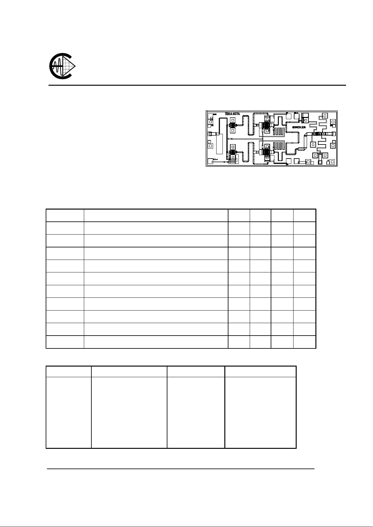
EMA407A
TENTATIVE DATA SHEET
20-32 GHz SUB-HARMONICALLY PUM P ED MIXER
FEATURES
• 20-32 GHz BANDWIDTH
• INTEGRATED LO AMPLIFIER
• 11 dB ± 1.5 dB TYPICAL CONVERSIO N LOSS
• 0.3 MICRO N RECE SSE D “MUSHROOM” GATE
• Si
3N4
PASSIVATION
• ADVANCED EPITAXIAL HETEROJUNCTION
The EMA407A chip is a sub-harmonically pumped
MMIC mixer with an integrated LO amplifier.
It can be used as an up-converter or down-converter.
ELECTRICAL CHARACTERISTICS1 (Ta = 25 OC)
SYMBOL PARAMETERS/TEST CONDITIONS MIN TYP MAX UNIT
FRF
RF Frequency Range 20 32 GHz
FLO
LO Frequency Range 9 18 GHz
FIF
IF Frequency Range 5 GHz
P
1dB
Input RF Power at 1dB Gain Compression 6 dBm
CL
Conversion loss 11 dB
∆ C
L
Flatness
± 1.5
dB
NF
Noise Figure 11 dB
LOdr
LO drive level 8 dBm
Idd
Power Supply Current 160 mA
Vdd
Power Supply Voltage 5 8 V
MAXIMUM RATINGS AT 25OC
SYMBOLS PARAMETERS ABSOLUTE1 CONTINUOUS2
Vds
Drain-Source Voltage
12V
8V
Vgs
Gate-Source Voltage
-8V
-3V
Ids
Drain Current
Idss
225mA
Igf
Forward Gate Current
55 mA
9mA
Pin
Input Power
dBm
@3dB Compression
Tch
Channel Temperature
175oC
150oC
Tstg
Storage Temperature
-65/175oC
-65/150oC
Pt
Total Power Dissipation
1.1 W
900 mW
Note: 1. E xceeding any of the a bove ratings may result in permanent damage.
2. E xceeding any of the a bove ratings may reduce MTTF below design goals.
Excelics Semiconductor, Inc., 2908 Scott Blvd., Santa Clara, CA 95054
Phone: (408) 970-8664 Fax: (408) 970-8998 Web Site: www.excelics.com
Chip Size 1060 x 2500 m icro ns
Chip Thicknes s: 75 ± 13 microns
All Dimensions In Microns
Page 2
EMA407A
TENTATIVE DATA SHEET
20-32 GHz SUB-HARMONICALLY PUM P ED MIXER
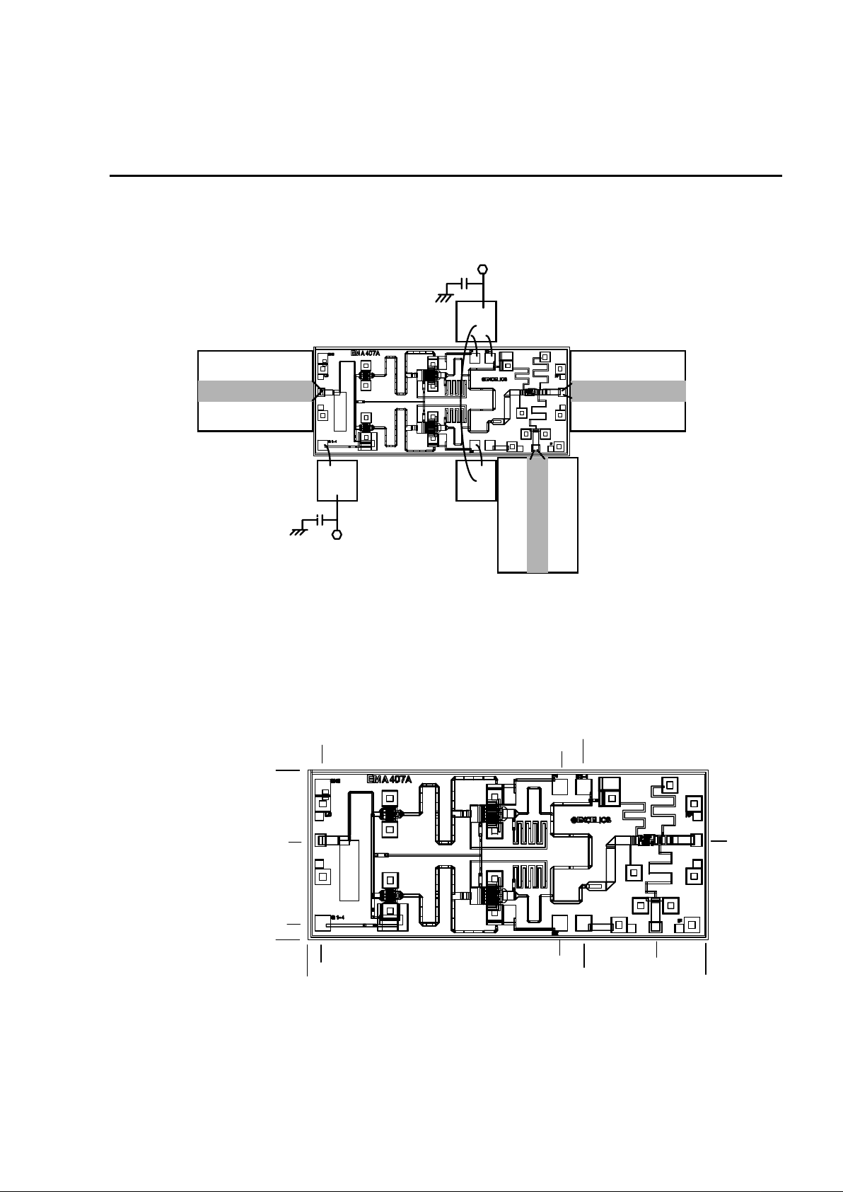
ASSEMBLY DRAWING
50pF
50pF
50 ohm line on Alumina
50pF
V
dd
V
GG
LO
50 ohm line on Alumina
RF
0.1 uF
0.1 uF
50 ohm line on Alumina
IF
The length of wires for RF and LO connections should be as short as possible. Use at least two wires, and separate the
wires to minimize the mutual inductance.
CHIP OUTLINE
Chip Size 1060 x 2500 m icro ns
Chip Thicknes s: 75 ± 13 microns
PAD Dimensions : 1. DC 100 x 100 microns
2. RF 80 x 68 microns
All Dimensions In Microns
0
0
1060
2500
100
1580
1730
620
620
1580
90
V
GG
1-4
V
D
2
V
D
1
LO
RF
IF
V
D3-4
GND for
DC check
1730
GND for
DC check
90
2170
Page 3

EMA407A
TENTATIVE DATA SHEET
20-32 GHz SUB-HARMONICALLY PUM P ED MIXER
TYPICAL APPLICATION PE RF ORMANCE
Linearity
( IF 1GHz , RF 20 G H z, LO 8dBm, V dd =6V)
-25
-20
-15
-10
-5
0
-15 -10 -5 0 5 10
RF input power [dBm
]
IF output power [dBm]
Frequency versus Conversion loss
(IF 1GHz, LO 8dBm, Vdd=6V)
-30
-25
-20
-15
-10
-5
0
15 20 25 30 35 40
frequenc
y
[GHz]
conversion loss [dB]
LO power versus Conversion loss
(IF 1GHz, Vdd=6V)
-50
-40
-30
-20
-10
0
0 5 10 15 20
LO power [dBm]
conversion loss [dB]
RF 26GHz
RF 28GHz
RF 32GHz
up-converter conversion loss
(IF 1GHz,LO 8dBm, Vds=6V)
-25
-20
-15
-10
-5
0
20 25 30 35 40
frequency [GHz]
conversion loss [dB]
2 LO - IF isolation
( IF 1GHz , LO 8dBm, Vdd =6V)
-25
-20
-15
-10
-5
0
15 20 25 30 35 40
frequency [GHz]
isolation [dB]
Page 4

EMA407A
TENTATIVE DATA SHEET
20-32 GHz SUB-HARMONICLLY PUM P ED MIXER
APPLICATION HINTS
The device should be die attached with Gold-Tin eutectic. Epoxy die attach is not recommended. Thermocompression
bonding of .7 mil to 1 mil diameter gold wire is recommended.
The sources of the transistors are directly via-hole grounded. A negative voltage is required to bias the gates of the
transistors. The gate voltage for the input stage must be provided at the RF input bonding pad, and the drain current for
the output stage must be provided through the output bonding pad. The drain bias circuits should be well bypassed do wn
to MHz frequencies to prevent oscillations. Some isolation should be provided between the two drain circuits at GHz
freque nc ies to prevent oscillatio ns. A lthough there is some b ypassing on chip of the VD1 and VG2 terminals, additio nal
bypass capa citors, placed close to th e chip, are recommended.
The gate and drain power supplies should be sequenced to turn on the negative gate voltage before the positive drain
voltage is applied. Turning on the full drain voltage before the gate voltage can cause excessive power dissipation or
destructive oscillations.
 Loading...