

Page 1
Excelics
EMA302B
PRELIMINARY DATA SHEET
22-26 GHz Medium Power MMIC
•
22-26 GHz BANDWIDTH
•
+28.0 dBm TYPICAL OUTPUT POWER
•
15 dB ± 1.5 dB TYPICAL POWER GAIN
•
TWO STAGE, INPUT PARTIALLY MATCHED,
OUTPUT MATCH OFF CHIP
•
0.3 MICRON RECESSED “MUSHROOM” GATE
•
Si
3N4
PASSIVATION
•
ADVANCED EPITAXIAL HETEROJUNCTION
PROFILE PROVIDES EXTRA HIGH POWER
EFFICIENCY, AND HIGH RELIABILITY
ELECTRICAL CHARACTERISTICS1 (Ta = 25 OC)
SYMBOL PARAMETERS/TEST CONDITIONS MIN TYP MAX UNIT
F
Operating Frequency Range 22 26 GHz
P
1dB
Ouput Power at 1dB Gain Compression 28 dBm
Gss
Small Signal Gain 15 dB
PAE
Power added efficiency at 1dB gain Compression 24 %
VSWR in
Input VSWR 2.5:1
VSWR out
Output VSWR 3.0:1
Ids1/Ids2
Drain Supply Currents for 1
st
& 2nd Stages 120/240 mA
Vdd
Power Supply Voltage 6 8 V
Rth
Thermal Resistance (Au-Sn Eutectic Attach) 18
o
C/W
Note: 1. Specifications are based on device mounted in application circuit.
D.C. characteristics for 1
st
& 2nd FETs follow those of EPA080A and EPA160A, respectively.
MAXIMUM RATINGS AT 25OC
SYMBOLS PARAMETERS ABSOLUTE2 CONTINUOUS3
Vds
Drain-Source Voltage
12V
8V
Vgs
Gate-Source Voltage
-8V
-3V
Ids1/Ids2
Drain Current
Idss
260 mA / 520 mA
Igsf1/Igsf2
Forward Gate Current
40 mA / 80 mA
7mA / 14 mA
Pin
Input Power
25dBm
@3dB Compression
Tch
Channel Temperature
175oC
150oC
Tstg
Storage Temperature
-65/175oC
-65/150oC
Pt
Total Power Dissipation
7.5 W
6.3 W
Note: 2. Exceeding any of the above ratings may result in permanent damage.
3. Exceeding any of the above ratings may reduce MTTF below design goals.
Excelics Semiconductor, Inc., 2908 Scott Blvd., Santa Clara, CA 95054
Phone: (408) 970-8664 Fax: (408) 970-8998 Web Site: www.excelics.com
Chip Thickness: 75 ± 13 microns
All Dimensions In Microns
65 50
85
50
50
1020
185
285
165
260
425
900
95
255
305
325
165
Page 2

EMA302B
PRELIMINARY DATA SHEET
22-26 GHz Medium Power MMIC
S-PARAMETERS
(CHIP WITHOUT EXTERNAL MATCHING CIRCUIT)
8V, 1/2 Idss
FREQ --- S11 --- --- S21 --- --- S12 --- --- S22 ---
(GHz) MAG ANG MAG ANG MAG ANG MAG ANG
1 0.955 -72.5 0.396 -138.9 0.000 177.5 0.019 -164.0
2 0.959 -110.2 6.670 107.4 0.001 73.5 0.155 -66.5
3 1.046 -126.7 10.324 -37.5 0.001 172.1 0.307 -100.9
4 1.061 -145.3 6.669 -15.9 0.004 165.1 0.346 -102.5
5 1.075 -156.4 15.100 -72.7 0.009 143.1 0.686 -101.5
6 0.916 -164.1 11.585 -154.3 0.010 100.1 0.754 -147.9
7 0.913 -163.5 5.883 172.1 0.007 95.3 0.536 -152.7
8 0.925 -164.5 3.726 154.9 0.007 103.4 0.484 -147.5
9 0.926 -165.4 2.660 142.4 0.009 108.3 0.484 -143.2
10 0.933 -165.4 2.109 133.0 0.005 100.8 0.517 -139.2
11 0.939 -165.7 1.747 123.3 0.006 115.3 0.543 -138.2
12 0.938 -164.6 1.520 114.7 0.007 117.3 0.571 -139.3
13 0.936 -164.4 1.372 106.1 0.008 131.5 0.598 -140.6
14 0.935 -165.7 1.278 97.5 0.008 121.1 0.631 -141.3
15 0.934 -167.8 1.229 88.1 0.008 120.0 0.649 -142.0
16 0.933 -168.4 1.249 79.2 0.008 104.3 0.679 -143.5
17 0.924 -169.2 1.272 68.3 0.007 111.8 0.695 -147.6
18 0.910 -172.3 1.358 56.3 0.010 84.6 0.743 -150.3
19 0.895 179.7 1.486 43.5 0.006 91.2 0.767 -147.5
20 0.868 171.0 1.688 28.1 0.006 87.5 0.797 -145.3
21 0.809 171.2 2.027 10.4 0.006 89.1 0.835 -154.2
22 0.713 164.0 2.606 -13.9 0.004 73.0 0.881 -156.3
22.5 0.613 162.1 3.032 -30.7 0.004 63.4 0.895 -159.4
23 0.473 164.8 3.459 -51.3 0.002 66.1 0.923 -162.8
23.5 0.347 -176.7 3.728 -76.5 0.003 121.7 0.926 -166.6
24 0.400 -147.1 3.618 -103.8 0.007 133.1 0.922 -169.1
24.5 0.558 -139.4 3.175 -129.8 0.009 122.1 0.897 -170.7
25 0.684 -141.3 2.647 -152.3 0.012 114.1 0.874 -169.7
25.5 0.764 -145.0 2.135 -171.9 0.012 99.9 0.861 -169.7
26 0.810 -147.9 1.708 170.0 0.014 90.0 0.879 -169.4
27 0.891 -153.0 1.142 141.0 0.014 85.5 0.870 -165.1
28 0.929 -156.3 0.750 113.7 0.016 84.5 0.851 -163.6
29 0.956 -156.5 0.502 91.7 0.019 81.6 0.839 -162.0
30 0.968 -155.1 0.338 78.3 0.026 64.0 0.852 -163.2
31 0.975 -152.8 0.228 52.3 0.018 49.3 0.846 -160.7
32 0.981 -153.0 0.157 31.8 0.013 54.7 0.856 -158.2
33 0.983 -154.1 0.118 14.7 0.012 57.3 0.902 -157.0
34 0.988 -153.9 0.113 -20.8 0.017 48.1 0.772 -160.7
35 0.983 -154.0 0.035 -18.1 0.011 78.3 0.879 -157.1
36 0.988 -155.5 0.025 -38.4 0.007 85.2 0.881 -157.3
37 0.997 -158.4 0.012 -53.2 0.007 107.8 0.867 -158.0
38 1.007 -157.6 0.006 112.6 0.009 109.7 0.862 -163.6
39 1.004 -153.8 0.002 165.9 0.008 89.1 0.851 -172.9
40 0.981 -154.9 0.015 -101.3 0.008 56.0 0.871 -177.9
Note: The data included 0.7 mils diameter au bonding wires:
2 input wires, 10 mils each; 4 output wires, 12 mils each.
Page 3

EMA302B
PRELIMINARY DATA SHEET
22-26 GHz Medium Power MMIC
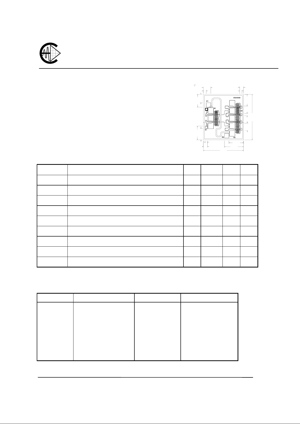
TYPICAL APPLICATION CIRCUIT
TYPICAL APPLICATION PERFORMANCE CHARACTERISTICS
Output Power at 1dB Compression
(dBm)
25
26
27
28
29
30
21 22 23 24 25 26 27
Frequency, GHz
Vdd=6V, Idd=490mA
Small S igna l Ga in ( dB )
5
7
9
11
13
15
17
20 22 24 26 28 30
Frequency, GHz
Vdd=6V, Idd=490mA
Page 4

EMA302B
PRELIMINARY DATA SHEET
22-26 GHz Medium Power MMIC
APPLICATION HINTS
The device should be die attached with Gold-Tin eutectic. Epoxy die attach is not recommended. Thermocompression
bonding of .7 mil to 1 mil diameter gold wire is recommended.
The EMA302B is partially input matched. Some input match and the output match must be provided off-chip. This
allows the use of optimal materials for matching networks to minimize loss, and provides for flexibility to optimize the
match for the application frequency. Typically the bond wire inductance will form part of the matching network, so bond
wire lengths must be controlled and repeatable.
The sources of the transistors are directly via-hole grounded. A negative voltage is required to bias the gates of the
transistors. The gate voltage for the input stage must be provided at the RF input bonding pad, and the drain current for
the output stage must be provided through the output bonding pa d. Appropriate bias networks must be provided off chip .
Typically a quarter wave microstrip line or bond wire will suffice. Adequate DC blocking and bypassing must also be
provided. A series resistance of about 50 ohms is recommended in the gate DC bias circuit of each FET to limit gate
current and suppress low frequency oscillations. The drain bias circuits should be well bypassed down to MHz
frequencies to prevent oscillations. Some isolation should be provided between the two drain circuits at GHz frequencies
to prevent oscillations. Although there is so me bypassing on chip of the VD1 and VG2 terminals, additional bypass
capacitors, placed close to the chip, are recommended.
The gate and drain power supplies should be sequenced to turn on the negative gate voltage before the positive drain
voltage is applied. Turning on the full drain voltage before the gate vo ltage can cause excessive power dissipation or
destructive oscillations.
 Loading...