

Page 1
GENERAL DESCRIPTION
The EM92600/1A series are developed for 46/49 MHz of 10 channels band frequency of cordless telephone
which is used in U.S.A.. These devices are dual phase-locked loop frequency synthesizers contained ROM
counters for receive and transmit loops with two independent phase detect circuits. A common reference
oscillator and reference divider are share by the receive and transmit circuits.
Other features include a lock detect circuit for the transmit loop, illegal code default, a buffered oscillator output
for mixing purposes in the system, 5KHz tone output . The EM92601A is designed for easy MPU interface. It
provides the same features as the EM92600A , but accepts channel programming via a clocked, serial input
instead of parallel BCD inputs. The EM92600A is selected channels via machanical switches of parallel BCD
input.
FEATURES
EM92600/1A
EM92600/1A
DUAL PLL FOR 46/49 MHZ CORDLESS PHONE
DUAL PLL FOR 46/49 MHZ CORDLESS PHONE
• Include oscillation circuit with external X-TAL (10.240 MHz).
• Unlock detector.
• 5KHz output for guard tone.
• Standby mode for power saving.
• 2.5 to 5.5V supply range.
• Baseset/Handset changeable.
• Available in 16 pin DIP or SOP.
• SERIES
Part Number Package Channel Selection
EM92600AP DIP parallel
EM92600AM SOP parallel
EM92601AP DIP serial
EM92601AM SOP serial
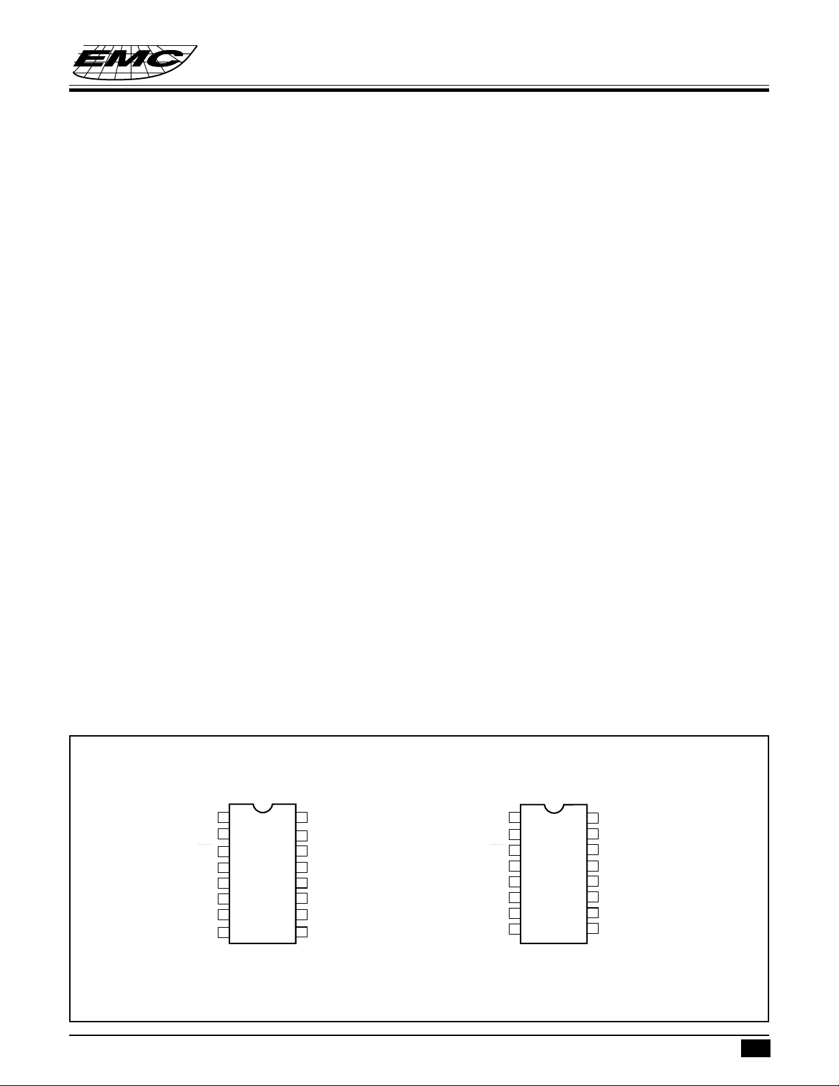
PIN ASSIGNMENTS
XTALO
MODE
SB
5K
D0
D1
D2
D3
EM92600A
1
16
2
15
3
14
4
13
5
12
6
11
7
10
8
9
XTALI
DD
V
RIF
PDR
SS
V
PDT
LD
TIF
XTALO
MODE
SB
5K
DI
CLK
NC
EN
EM92601A
1
16
2
15
3
14
4
13
5
12
6
11
7
10
8
9
XTALI
DD
V
RIF
PDR
SS
V
PDT
LD
TIF
* This specification are subject to be changed without notice.
4.23.1995
1
Page 2
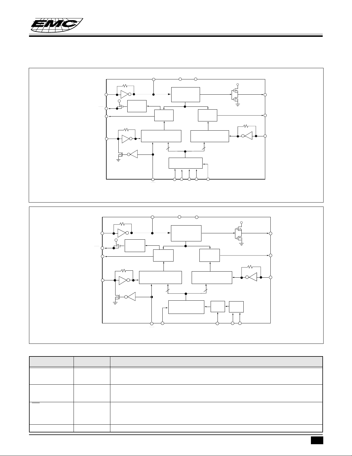
FUNCTIONAL BLOCK DIAGRAM
XTAL1
PDT
LD
DD
V
Lock
detector
XTAL0
phase
detector
V
DD
V
Reference
counter
divide by 2048
EM92600/1A
DUAL PLL FOR 46/49 MHZ CORDLESS PHONE
SS
DD
V
5K
Phase
detector
PDR
XTAL1
LD
PDT
TIF
TIF
14 bits divide by N
Transmit counter
SB
b13-b0
ROM 32*28
& decoder logic
D3
14 bits divide by N
D2D1D0
receive counter
b27-b14
MODE
RIF
EM92600A block diagram
DD
V
counter
SS
Phase
detector
14 bits divide by N
receive counter
b27-b14
V
DD
5K
PDR
RIF
XTAL0
V
DD
Lock
detector
phase
detector
14 bits divide by N
Transmit counter
V
Reference
divide by 2048
b13-b0
4 bits
latch
4 bits
S/R
DICLKEN
SB
ROM 32*28
& decoder logic
MODE
EM92601A block diagram
PIN DESCRIPTIONS
Symbol Pin No. Function
XTALO O This ouput generates reference frequency when it is connected to pin 16 with
external OSC of which frequency is 10.240MHz
MODE I Base/remote changing. Internal pull down.
=base,VSS=remote.
V
DD
SB I The standby pin is uses to save power when no transmit. Internal pull down.
High: transmit and receive active
Low: receive acts only
5K O The signal derived from the reference oscillator. 5KHz output.
* This specification are subject to be changed without notice.
4.23.1995
2
Page 3

EM92600/1A
DUAL PLL FOR 46/49 MHZ CORDLESS PHONE
Symbol I/O Function
D0 I The channel selected pin. LSB.(intenal pull down)
D1 I The channel selected pin. (internal pull down)
D2 I The channel selected pin. (internal pull down)
D3 I The channel selected pin. MSB.(internal pull down)
Di I The serial input data pin.
CLK I Clock input. Each low to high transition of the clock shifts one bit of data into
the on-chip shift register.
NC - Not connect.
EN I The enable pin controls the data transfer from the shift register to the 4-bit latch.
A low to high transition latches the data.
TIF I Input to programmable divider of Tx. AC coupling with VCO. Min input voltage
is 200mVpp.
LD O Unlock detector output. VDD level: unlock.
PDT O Phase detector output for Tx. PDT detects the phase error from Tx PLL and its
output is connected to external low pass filter.
V
SS
- Ground.
PDR O Phase detector output for Rx. PDR detects the phase error from Rx PLL and its
output is connected to external low pass filter.
RIF I Input of programmable divider for Rx.AC coupling with VCO. Min input voltage
is 200mVpp.
V
DD
- Power supply.
XTAL1 I To connect crystal ( 10.240MHz ) and capacitor.
ABSOLUTE MAXIMUM RATINGS
Symbol Rating Value Unit
V
DD
V
IN
I
IN,IOUT
I
DD,ISS
T
A
T
STG
* This specification are subject to be changed without notice.
DC supply voltage -0.5 to +6 V
Input voltage -0.5 to VDD+0.5 V
DC current drain per pin 10.0 mA
DC current drain VDD or VSS pins 30.0 mA
Operating temperature range -30 to +75 °C
Storage temperature range -65 to +150 °C
4.23.1995
3
Page 4

DUAL PLL FOR 46/49 MHZ CORDLESS PHONE
DC ELECTRICAL CHARACTERISTICS
(T
25°C unless otherwise noted )
A=
Parameter Sym. Min. Typ. Max. Unit Condition
EM92600/1A
IL
IH
2.5 - 5.5 V
- 0.8 V VDD=3V
2.2 -
- 0.05 V VDD=3V
2.95 -
µAvIL=0
Operating voltage V
Input voltage V
V
Output voltage V
V
Input low current I
DD
OL
OH
IL
-36 - pin 16,14,9
-0.06 - pin 2~8
Input high current I
IH
µAvIH=VDD-0.5V
- 36 pin 16,14,9
- 120 pin 2~8
Output current I
Standby current I
Operating current I
OH
I
OL
DS
DO
-0.2 - mA VOH=2.6V
0.2 - VOL=0.4V
- 1.5 mA VDD=3V, note1
- 3.0 mA VDD=3V, note2
(0.2Vp-p input at RIF,TIF)
3-state leakage current I
OZ
- ±1 µAVDD=5V
Note 1: XTALin: 10.24MHz ; MODE:VDD; SB:VSS; TIF=20MHz(200 mVp-p); RIF=40MHz(200 mVp-p); others
are open.
Note 2: XTALin: 10.24MHz ; MODE:V
; SB:VDD; TIF=20MHz(200 mVp-p); RIF=40MHz(200 mVp-p); others are
DD
open.
AC ELECTRICAL CHARACTERISTICS
Parameter Sym. Min. Typ. Max. Unit Condition
Output rise time T
Output fall time T
Input rise and fall time T
OSC in T
Maximum frequency F
R
F
R
F
MAX
input =sine wave 0.2Vp-p 50 MHz RIF (V
Setup time data to clock T
SU
Enable to clock 100
200 nS
Hold time T
H
80 nS EM92601A only
clock to data
Recovery time T
REC
80 nS EM92601A only
Enable to clock
Input pulse width T
W
80 nS EM92601A only
clock and Enable
* This specification are subject to be changed without notice.
200 nS VDD=3V
200 nS VDD=3V
5 µS XTAL1
VDD=3V
12 XTAL1
DD
50 TIF
EM92601A only
=3V)
4.23.1995
4
Page 5
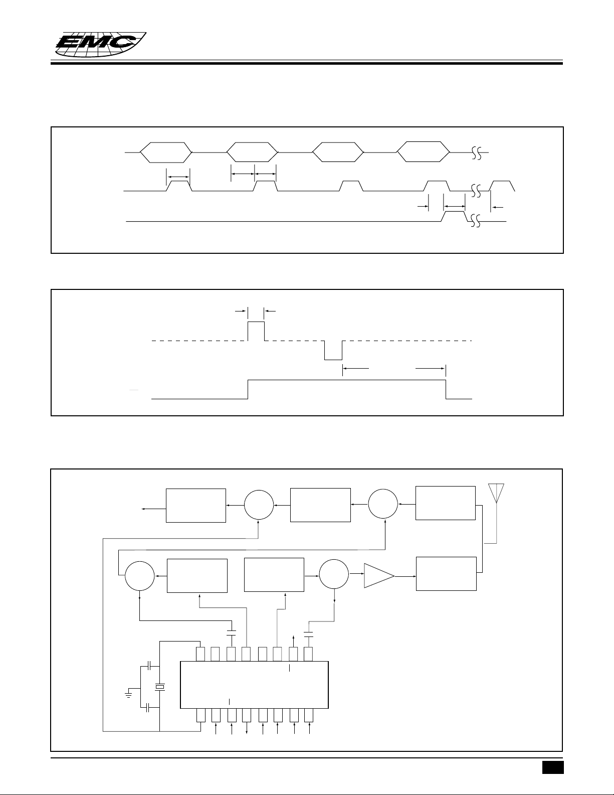
TIMING DIAGRAM
EM92600/1A
DUAL PLL FOR 46/49 MHZ CORDLESS PHONE
Data
Clock
Enable
PDT
LD
tw
1 st
CLK
D2 D1
th
tsu
2 nd
CLK
EM92601A Timing
1.6µS
Unlock Timing
3 rd
CLK
6.4±0.4mS
D0D3
4 th
CLK
tsu
tw
Previous
Data Latched
trec
1 st
CLK
APPLICATION CIRCUIT
0.455MHz
RX
VCO
10.240
MHz
2ND IF
16 15 14
XTAL1
XTAL0
12 3
13 12 11
RIF
VDD
MODESB5K
4
PDR
2ND
MIX
LPFLPF
VSS
PDT
DO/DI
D1/CLK
56
10
LD
D2/NC
7
1ST IF
9
TIF
D3/EN
8
TX
VCO
1ST
MIX
BPF
BPF
* This specification are subject to be changed without notice.
4.23.1995
5
Page 6

DUAL PLL FOR 46/49 MHZ CORDLESS PHONE
DIVIDE RATIO AND VCO FREQUENCIES
Base Input Rx (Fref=5KHz) Tx=(Fref=5KHz)
(MODE=1) CH
D3 D2 D1 D0 FRx (MHz) FVCO(MHz) N FTx(MHz) FVCO(MHz) N
0 0 0 1 1 49.670 38.975 7795 46.610 46.610 9322
0 0 1 0 2 49.845 39.150 7830 46.630 46.630 9326
0 0 1 1 3 49.860 39.165 7833 46.670 46.670 9334
0 1 0 0 4 49.770 39.075 7815 46.710 46.710 9342
0 1 0 1 5 49.875 39.180 7836 46.730 46.730 9346
0 1 1 0 6 49.830 39.135 7827 46.770 46.770 9354
0 1 1 1 7 49.890 39.195 7839 46.830 46.830 9366
1 0 0 0 8 49.930 39.235 7847 46.870 46.870 9374
1 0 0 1 9 49.990 39.295 7859 46.930 46.930 9386
1 0 1 0 10 49.770 39.275 7855 46.970 46.970 9394
1 0 1 1 49.970 39.275 7855 46.970 46.970 9394
1 1 0 0 49.970 39.275 7855 46.970 46.970 9394
1 1 0 1 49.970 39.275 7855 46.970 46.970 9394
1 1 1 0 49.970 39.275 7855 46.970 46.970 9394
1 1 1 1 49.970 39.275 7855 46.970 46.970 9394
0 0 0 0 49.970 39.275 7855 46.970 46.970 9394
EM92600/1A
REMOTE Input Rx (Fref=5KHz) Tx=(Fref=5KHz)
(MODE=0) CH
D3 D2 D1 D0 FRx (MHz) FVCO(MHz) N FTx(MHz) FVCO(MHz) N
0 0 0 1 1 46.610 35.915 7183 49.670 49.670 9934
0 0 1 0 2 46.630 35.935 7187 49.845 49.845 9969
0 0 1 1 3 46.670 35.975 7195 49.860 49.860 9972
0 1 0 0 4 46.710 36.015 7203 49.770 49.770 9954
0 1 0 1 5 46.730 36.035 7207 49.875 49.875 9975
0 1 1 0 6 46.770 36.075 7215 49.830 49.830 9966
0 1 1 1 7 46.830 36.135 7227 49.890 49.890 9978
1 0 0 0 8 46.870 36.175 7235 49.930 49.930 9986
1 0 0 1 9 46.930 36.235 7247 49.990 49.990 9998
1 0 1 0 10 46.970 36.275 7255 49.970 49.970 9994
1 0 1 1 46.970 36.275 7255 49.970 49.970 9994
1 1 0 0 46.970 36.275 7255 49.970 49.970 9994
1 1 0 1 46.970 36.275 7255 49.970 49.970 9994
1 1 1 0 46.970 36.275 7255 49.970 49.970 9994
1 1 1 1 46.970 36.275 7255 49.970 49.970 9994
0 0 0 0 46.970 36.275 7255 49.970 49.970 9994
* This specification are subject to be changed without notice.
4.23.1995
6
 Loading...