

Page 1

1
* This specification are subject to be changed without notice.
9.14.2001
EM83040B
LCD CONTROLLER
PreliminaryPreliminary
PreliminaryPreliminary
Preliminary
GENERAL DESCRIPTION
The EM83040B is a dot matrix LCD driver, which is fabricated by low power CMOS technology. This chip
includes 80-bits shift register, 80 bits data latch and 80 bits level driver. A LCD RAM inside can be mapping
to LCD signal. It converts RAM data to parallel data and output waveform to LCD.
FEATURES
(1) Supply power: 2.5~5.5V
(2) LCD drive voltage: 3.6 to15V
(3) Internal RAM: 2.5k x 4 bits
(4) RAM can be controlled by eight signals including four bits data bus.
(5) Duty: 1/32, 1/48, 1/64, 1/80
(6) Build in DC/DC converter: double, triple, quad and five times.
(7) Modularized function: connect to another 83040B to extent LCD matrix
(8) One DC converter enabled and other 83040B can share with this.
(9) Internal regulator output for DC/DC converter controlled by control register.
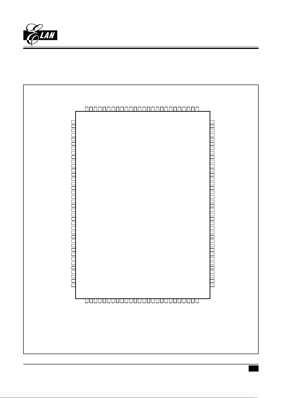
(10) Chip form (EM83040BH), 128 pin package (14mm x 20mm EM83040BAQ), 160 pin package
(EM83040BBQ)
(11) Bias: 1/5 (32 COMMON), 1/7 (48 COMMON), 1/9 (64 and 80 COMMON) fixed by internal circuit.
(12) Internal RC clock about 250 KHz.
APPLICATION
(1) Data Bank
(2) LCD toy
(3) Education computer
Page 2
* This specification are subject to be changed without notice.
EM83040B
LCD CONTROLLER
2
9.14.2001
PreliminaryPreliminary
PreliminaryPreliminary
Preliminary
PIN ASSIGNMENTS
EM83040BAQ
1
2
3
4
5
6
7
8
9
10
11
12
13
14
15
16
17
18
19
20
21
22
23
24
25
26
27
28
29
30
31
32
33
34
35
36
37
38
39404142434445464748495051525354555657585960616263
64
102
101
100
99
98
97
96
95
94
93
92
91
90
89
88
87
86
85
84
83
82
81
80
79
78
77
76
75
74
73
72
71
70
69
68
67
66
65
128
127
126
125
124
123
122
121
120
119
118
117
116
115
114
113
112
111
110
109
108
107
106
105
104
103
MAIN
M1
M0
EN
NC
NC
NC
NC
RAMEN
RAMADS
RAMW
RAMR
RAMD3
RAMD2
RMAD1
RAMD0
LOAD
VDD
GND
VOUT
VSS4
VSS3
CB
CA
VSS2+
VSS2-
V1
V2
VREG
NC
NC
NC
NC
NC
V3
V4
V5
O0
O1O2O3O4O5O6O7O8O9
O10
O11
O12
O13
O14
O15
O16
O17
O18
O19
O20
O21
O22
O23
O24
O25
O26
O53
O52
O51
NC
NC
NC
NC
NC
O50
O49
O48
O47
O46
O45
O44
O43
O42
O41
O40
O39
O38
O37
O36
O35
O34
O33
O32
O31
O30
NC
NC
NC
NC
NC
NC
O29
O28
O27
O79
O78
O77
O76
O75
O74
O73
O72
O71
O70
O69
O68
O67
O66
O65
O64
O63
O62
O61
O60
O59
O58
O57
O56
O55
O54
EM83040BAQ
Page 3
3
* This specification are subject to be changed without notice.
9.14.2001
EM83040B
LCD CONTROLLER
PreliminaryPreliminary
PreliminaryPreliminary
Preliminary
EM83040BBQ
EM83040BBQ
VSS4
VSS3
+
-
VREG
VOUT
Page 4
* This specification are subject to be changed without notice.
EM83040B
LCD CONTROLLER
4
9.14.2001
PreliminaryPreliminary
PreliminaryPreliminary
Preliminary
BLOCK DIAGRAM
VREG
V1
REG(5~0)
BIAS
MUX
: : : : :
M1,M0
Buffer1
Buffer2
Buffer3
Buffer4
Buffer5
Regulator
IR(2~0)
Resistance
ratio
VOUT
VSS4
VSS3
CA
CB
VSS2+
VSS2-
Page 5
5
* This specification are subject to be changed without notice.
9.14.2001
EM83040B
LCD CONTROLLER
PreliminaryPreliminary
PreliminaryPreliminary
Preliminary
PIN DESCRIPTIONS
Symbol I/O Function
VDD Power System power supply
GND Power Ground
VOUT Power Voltage converter input/output pin
Connect this pin to GND through capacitor
EN=1,VOUT=VDD
VSS4 Power Step-up capacitor
EN=1, VSS4=VDD
VSS3 Power Step-up capacitor
EN=1, VSS3=VDD
VSS2+ Power Step-up capacitor
EN=1, VSS2=VDD
VSS2- Power Step-up capacitor
VREG Power Output voltage regulator terminal. Provides the voltage between V1 and GND
through a resistive voltage divider.
MAIN I Master or slave control signal.
MAIN=1, master unit
MAIN=0, slave unit
EN I This pin control whole chip power. This chip will work when this pin is connected
to ground. And whole chip will disable when connect to VDD voltage.
EN=0 and MAIN=1 the chip will generate VSS2+, VSS2-
VSS3, VSS4, VOUT, LOAD signal and internal RC clock.
EN=1, standby mode
M1 I Mode select
M0 I Mode select
RAMEN RAM read and write control signal.
1 => can not read and write. 0=> can read and write.
RAMADS RAM data select signal
1=> RAM Data, 0=>Address
RAMW RAM write signal, low write
RAMR RAM read signal, low read
RAMD3~RAM RAM data or address bus
D0
LOAD I/O LCD load signal between one COMMON signal to another.
MAIN=1, the master unit will output LOAD signal.
MAIN=0, the slave will accept the signal from master unit.
CA I Coupling capacitor
CB I Coupling capacitor
V1~V5 I Reference voltage input, highest V1°K lowest V5
O1~O80 O LCD waveform output
Page 6
* This specification are subject to be changed without notice.
EM83040B
LCD CONTROLLER
6
9.14.2001
PreliminaryPreliminary
PreliminaryPreliminary
Preliminary
FUNCTION DESCRIPTIONS
(1)User can use MAIN pin to chose master unit or slave unit.
MAIN Unit Function
1 MASTER Generate these signals:
Load, CA, CB, VSS2+, VSS2-, VSS3, VSS4, VOUT
Internal RC clock
0 SLAVE Accept these Master unit signals
Load, VOUT, V1, V2, V3, V4, V5
No internal RC clock
(2)User can use M1,M2 to choose four modes. As followed
MASTER MAIN M1 M0 Segment Common BIAS
Mode1 1 0 0 O(16:1)=S(16:1) O(80:17)=C(64:1) 1/9
Mode2 1 0 1 O(80:1)=C(80:1) 1/9
Mode3 1 1 0 O(32:1)=S(32:1) O(80:33)=C(48:1) 1/7
Mode4 1 1 1 O(48:1)=S(48:1) O(80:49)=C(32:1) 1/5
SLAVE MAIN M1 M0 Segment Common BIAS
Mode1 0 0 0 O(80:1)=S(80:1) 1/9
Mode2 0 0 1 O(80:1)=S(80:1) 1/9
Mode3 0 1 0 O(80:1)=S(80:1) 1/7
Mode4 0 1 1 O(80:1)=S(80:1) 1/5
* S=Segment, C=Common
* (M1, M0) for Master must same as Slave unit
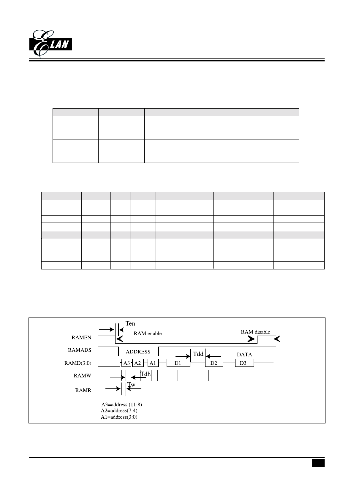
(3)RAM control
Write mode
FIG. 3
LCD RAM can be written or read with control signal. The RAMEN pin can select a RAM which can be read or
write. The RAMADS pin can select whether
Page 7
7
* This specification are subject to be changed without notice.
9.14.2001
EM83040B
LCD CONTROLLER
PreliminaryPreliminary
PreliminaryPreliminary
Preliminary
RAMD(3:0) are data or address of RAM. At the address mode, RAMADS is low and user should sent address
three times, from address (11:8) to address (3:0). Then it will go into data mode when RAMADS is high. In data
mode, user can sent one or more nibble data which address can be increased by internal counter.
Once the RAMEN pin is high, the RAM can not read and write.
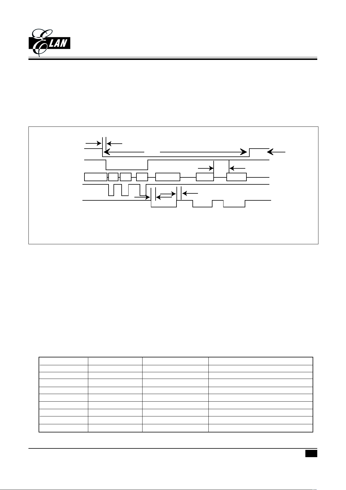
(4)Read control
RAMEN
RAMADS
RAMD(3:0)
RAMW
RAMR
A3 A2 A1 D1 D2 D3
RAM enable
RAM disable
ADDRESS
DATA
A3=address (11:8)
A2=address(7:4)
A1=address(3:0)
Ten
Tdv
Tdh
Tdd
FIG. 4
As same as write mode, user has to sent address three times. And read data from RAM one by one which address
can be increased by internal counter. Note!! Be sure to make RAMR low pulse 2uS (Tdv +data) width and 2uS
(Tdd) high width at least.
(5)RAM mapping
RAM address is from 0 to address 2562
User fill “1” to LCD RAM, LCD driver will generate “light” waveform. Otherwise, it will generate a “dark”
waveform. The LCD RAM area is mapped to segment 1 to segment 80 from address 0 to address 19. And user
can refer to fig.5 and Table 1 to get the idea of LCD ram mapping. The other RAM can use as general RAM for
data storage if not mapping to LCD display. And the RAM of address 2560, 2561 and 2562 is control registers.
Table 1: LCD mapping RAM area
Common Segment Master/slave Display area
32 48 Master 1,2,3
32 80 Slave 1,2,3,4
48 32 Master 1,2,5,6
48 80 Slave 1,2,3,4,5,6,7
64 16 Master 1,5,8
64 80 Slave 1,2,3,4,5,6,7,8,9
80 0 Master No mapping RAM
80 80 Slave 1,2,3,4,5,6,7,8,9,10
Any Any Any Area 11 is general RAM
Page 8

* This specification are subject to be changed without notice.
EM83040B
LCD CONTROLLER
8
9.14.2001
PreliminaryPreliminary
PreliminaryPreliminary
Preliminary
Fig.5
As same as write mode , user has to sent address three times. And read data from RAM one by one which
address can be increased by internal counter. NOTE!! Be sure to make RAMR low pulse 2 µS (Tdv+data)
width and 2 µS (Tdd) high width at least.
(5) RAM mapping
RAM address is from 0 to address 2559
User fill “1” to LCD RAM , LCD driver will generate “light” waveform. Otherwise , it will generate a
“dark” waveform. The LCD RAM area is mapped to segment 1 to segment 80 from address 0 to address
19. And user can refer to fig.5 to get the idea of LCD ram mapping. The other RAM can use as general
RAM for data storage. And the RAM of address 2560 is a control register.
address2559 ...................
address0031 ...................
address0063 ................... address0051 ........................................................
..........................
address1023 ...................
address1535 ...................
address2047 ...................
address2547 ......................................................................................................................... address2528
address2035 ......................................................................................address2019...............address2016
address1523 ............................................................address1511........................................address1504
address1011 .......................address1003 ............................................................................. address0992
LCD RAM
Area 10
Area 11
Area 9
Area 8
Area 5
Area 6
Area 7
Area 4 Area 3
Area 2
Area 1
Address 2560,2561
2562 Control register
Address 2560,2561,2562
Control register
EMPTY AREA
:
:
:
:
:
:
:
:
:
:
:
:
:
:
:
:
................................... address0032
address0019 ...................
b3 b2 b1 b0 ...................
s80s79s78s77
s4 s3 s2 s1
s48 s32
s16
address0011................ address7...........
address0003............... address0000
COM80
COM64
COM48
COM32
COM2
COM1
b3 b2 b1 b0
Page 9

9
* This specification are subject to be changed without notice.
9.14.2001
EM83040B
LCD CONTROLLER
PreliminaryPreliminary
PreliminaryPreliminary
Preliminary
(6) LCD waveform
Fig.6
V1
V2
V3
V4
V5
GND
V1
V2
V3
V4
V5
GND
V1
V2
V3
V4
V5
GND
V1
V2
V3
V4
V5
GND
V1
V2
V3
V4
V5
GND
frame
com0
com1
com2
seg
seg
light
dark
Page 10

* This specification are subject to be changed without notice.
EM83040B
LCD CONTROLLER
10
9.14.2001
PreliminaryPreliminary
PreliminaryPreliminary
Preliminary
(7) Control register
Address Bit3 Bit2 Bit1 Bit0
2560 IRS IR2 IR1 IR0
2561 REG3 REG2 REG1 REG0
2562 PS1 PS0 REG5 REG4
X: don’t care
Default status of Address 2560,2561 and 2562, respectively: 0010, 0000, 0000
Address 2562 bit3~2(PS1, PS0) be selected:
Use settings PS1 PS0 Step-up V V/F External
circuit regulator circuit voltage input
circuit
Only the internal power
supply is used 1 1 Ο OOX
Only the V regulator
circuit and the V/F circuit 1 0 X O O VOUT
are used
Only the V/F circuit is
used 0 1 X X O V1
Only the external power
supply is used 0 0 X X X V1 to V5
Address 2562 bit1~0 and 2561 bit3~0 (Reg5~Reg0) is selected the VEV value
REG5~REG0 V
EV
VEV step
000000 1.2 V
000001 1.212 V
↓↓
011111 1.572 V 0.012V
100000 1.584 V
↓↓
111110 1.944 V
111111 1.956 V
V
1
R
a
R
b
V
REG
V
EV
VOUT
Fig.7
Page 11

11
* This specification are subject to be changed without notice.
9.14.2001
EM83040B
LCD CONTROLLER
PreliminaryPreliminary
PreliminaryPreliminary
Preliminary
Address 2560 bit3 (IRS) is internal resistor selected
IRS=0: internal regulator resistor is used.
IRS=1: internal regulator resistor is not used. (External resistor is used)
Address 2560 bit0~2(IR2, IR1, IR0) is selected for the V1 voltage regulator internal resistance ratio
IR2~IR0 Resistor ratio (1+Rb/Ra)
0 0 0 3.0
0 0 1 3.5
0 1 0 4.0
0 1 1 4.5
1 0 0 5.0
1 0 1 5.5
1 1 0 6.0
1 1 1 6.5
The V1 voltage can be calculated using equation A over the range where VDD < V1 ≤ VOUT
V1=(1+Rb/Ra) • V
EV
*(94%~97%) (Equation A)
(94%~97%) depend on loading
Example: Default: IRS=0 (internal regulator resistor is used), (IR2, IR1, IR0)=(0, 1, 0), and (REG5~0)=(000000)
V1=(1+Rb/Ra) • VEV*(94%~97%)=4.0 • 1.2*(94%~97%)= 4.51 V~4.65V
When IRS=0 (internal regulator resistor is used), (IR2, IR1, IR0)=(0, 1, 1), and (REG5~0)=(100000)
V1=(1+Rb/Ra) • VEV*(94%~97%)=4.5 • 1.584*(94%~97%)= 6.7~6.91 V
FIG. 8 show the V1 voltage measured by values of the internal resistance ratio resistor (1+Rb/Ra) for V1 voltage
adjustment and electric volume resister (REG5~REG0).
FIG. 8 The output voltage V1 is determined by function of the V1 voltage regulator ratio register (1+Rb/Ra), and
the electric volume resister (REG5~REG0).
(8) The step-up voltage circuit
Case of the double step-up, the triple step-up and Case of the quad step-up VOUT is output voltage pin the bias
voltage V1 is supported from VREG.
(a) Double step-up, (b) Triple step-up, (c) Quad step-up (d) five times step-up C1=0.47 to 1.0£gf, C2=1.0 to
4.7uf
(a) VOUT=2*VDD (b) VOUT=3*VDD (c) VOUT=4*VDD (d) VOUT=5*VDD
FIG. 9
EM83040B
VOUT
VSS4
VSS3
CB
CA
VSS2+
VSS2-
VREG
V1
V2
V3
V4
V5
C2
C2
C1
C2
C2
C2
C1
EM83040B
VOUT
VSS4
VSS3
CB
CA
VSS2+
VSS2-
VREG
V1
V2
V3
V4
V5
C2
C2
C2
C2
C1
EM83040B
VOUT
VSS4
VSS3
CB
CA
VSS2+
VSS2-
VREG
V1
V2
V3
V4
V5
C2
C2
C2
C2
C1
EM83040B
VOUT
VSS4
VSS3
CB
CA
VSS2+
VSS2-
VREG
V1
V2
V3
V4
V5
C2
Page 12

* This specification are subject to be changed without notice.
EM83040B
LCD CONTROLLER
12
9.14.2001
PreliminaryPreliminary
PreliminaryPreliminary
Preliminary
(9) Reference circuit examples are as following FIG. 10
(a) Only the internal power supply is used, control register (PS1, PS0, IRS)=(1,1,0)
(b) Only the internal power supply is used, control register (PS1, PS0, IRS)=(1,1,1) When internal regulator
resistor is not used (external resistor is used), V1=VREG*(1+Rb’/Ra’)
(c) Only the V regulator circuit and the V/F circuit are used, control register (PS1, PS0, IRS)=(1,0,0)
(d) Only the V regulator circuit and the V/F circuit are used, control register (PS1, PS0, IRS)=(1,0,1),
When internal regulator resistor is not used (external resistor is used), V1=VREG*(1+Rb’/Ra’)
(e) Only the V/F circuit is used, control register (PS1, PS0)=(0,1)
(f) Only the external power supply is used, control register (PS1, PS0)=(0,0)
EM83040B
VOUT
VSS4
VSS3
CB
CA
VSS2+
VSS2-
VREG
V1
V2
V3
V4
V5
C2
C2
C2
C2
C1
MAIN
VDD
EM83040B
VOUT
VSS4
VSS3
CB
CA
VSS2+
VSS2-
VREG
V1
V2
V3
V4
V5
C2
C2
C2
C2
C1
Rb’
Ra’
MAIN
VDD
EM83040B
VOUT
VSS4
VSS3
CB
CA
VSS2+
VSS2-
VREG
V1
V2
V3
V4
V5
C1
EXTERNAL
POWER
SUPPLY
MAIN
VDD
EM83040B
VOUT
VSS4
VSS3
CB
CA
VSS2+
VSS2-
VREG
V1
V2
V3
V4
V5
C1
Rb’
Ra’
EXTERNAL
POWER
SUPPLY
VDD
EM83040B
VOUT
VSS4
VSS3
CB
CA
VSS2+
VSS2-
VREG
V1
V2
V3
V4
V5
C1
EXTERNAL
POWER
SUPPLY
VDD
EM83040B
VOUT
VSS4
VSS3
CA
CB
VSS2+
VSS2-
VREG
V1
V2
V3
V4
V5
EXTERNAL
POWER
SUPPLY
VDD
(a) (b) (c)
(d) (e) (f)
FIG. 10
Page 13

13
* This specification are subject to be changed without notice.
9.14.2001
EM83040B
LCD CONTROLLER
PreliminaryPreliminary
PreliminaryPreliminary
Preliminary
ABSOLUTE MAXIMUM RATINGS
Rating Symbol Value Unit
DC SUPPLY VOLTAGE VDD <3.5 V
INPUT VOLTAGE Vin -0.5 TO Vdd ±0.5 V
OPERATING TEMPERATURE RANGE Ta -30 TO 80 °C
STEP-UP VOLTAGE VOUT <18 V
AC ELECTRICAL CHARACTERISTICS (T
A
= -30°C ~ 80°C, VDD=3V VSS=0V)
Parameter Sym. Min. Typ. Max. Unit
RC clock variable Vrc -20 +20 %
Frame period Tframe 1/64 S
Load period Tload 31 µS
Enable time Ten 30 µS
Write low pulse Tw 2 µS
Data hold time Tdh 500 nS
Data to data time Tdd 2 µS
Data valid time Tdv 1500 nS
DC ELECTRICAL CHARACTERISTICS (T
A
= -30°C ~ 80°C, VDD=3V±5%, VSS=0V)
Parameter Sym. Min. Typ. Max. Unit Condition
Input voltage V
DD
2.5 5.5 With double step-up
2.5 5.5 With triple step-up
2.5 4.0 With quad step-up
2.5 3.3 With five times step-up
Output Low current I
OL
-100 µAVDD=3V
Standby current I
SD
14µA EN=1
Operating voltage I
OP
180 220 µA EN=0, MAIN =1(MASTER) , DC
converter enable, Five times step-up
(M1, M0)=(1,1) V1=11V, 250KHz
clock, No load
40 70 µA EN=0 . MAIN =0 (SLAVE) ,DC
converter enable, Five times step-up
(M1, M0)=(1,1) V1=11V, 250KHz
clock, No load
Current of a buffer (V1 toV5) Ibuf 4 6 10 µA Current of a buffer
Voltage variation of regulator Vreg V-0.1 V V+0.1 V
Regulator current Ireg 10 15 µA
BIAS resister R_bias 1800 2000 2200 kΩ
V
Page 14

* This specification are subject to be changed without notice.
EM83040B
LCD CONTROLLER
14
9.14.2001
PreliminaryPreliminary
PreliminaryPreliminary
Preliminary
AC TIMING
Fig .11 LCD control timing
LCD control timing
Fig .12 LCD RAM write mode
FRAME
LOAD
S0 S1 S2 S3 SN
C0 C1
CM C0
POSITIVE FRAME NEGATIVE FRAME
Tframe
Tload
EN
RAMEN
RAMADS
RAMD(3:0)
RAMW
RAMR
A3 A2 A1 D1 D2 D3
RAM enable
RAM disable
ADDRESS DATA
A3=address(11:8)
A2=address(7:4)
A1=address(3:0)
Tw
Tdh
Ten
Tdd
Page 15

15
* This specification are subject to be changed without notice.
9.14.2001
EM83040B
LCD CONTROLLER
PreliminaryPreliminary
PreliminaryPreliminary
Preliminary
Fig .13 LCD RAM read mode
APPLICATION CIRCUIT
(1) C32 x S48
Fig .14
RAMEN
RAMADS
RAMD(3:0)
RAMW
RAMR
A3 A2 A1 D1 D2 D3
RAM enable
RAM disable
ADDRESS DATA
A3=address (11:8) A2=address(7:0) A1=address(3:0)
D1= first nibble D2=second nibble D3=third nibble data
Ten
Tdv
Tdh
Tdd
VDD
GND
MAIN
M1
M0
EN
RAMEN
RAMADS
RAMW
RAMR
RAMD(3:0)
LOAD
VOUT
VSS4
VSS3
CB
CA
VSS2+
VSS2VREG
V1
V2
V3
V4
V5
NC
NC
VDD
VDD
VDD
Page 16

* This specification are subject to be changed without notice.
EM83040B
LCD CONTROLLER
16
9.14.2001
PreliminaryPreliminary
PreliminaryPreliminary
Preliminary
(2) C32 x S128
Fig .15
(3) C48 x S112
Fig .16
VDD
GND
MAIN
M1
M0
EN
RAMEN
RAMADS
RAMW
RAMR
RAMD(3:0)
LOAD
VOUT
VSS4
VSS3
CB
CA
VSS2+
VSS2VREG
V1
V2
V3
V4
V5
LOAD
NC
VDD
VDD
VDD
S127 ...... S80
VOUT
C31
:
:
C0
MASTER
VDD
GND
MAIN
M1
M0
EN
RAMEN
RAMADS
RAMW
RAMR
RAMD(3:0)
LOAD
VOUT
VSS4
VSS3
CB
CA
VSS2+
VSS2VREG
V1
V2
V3
V4
V5
LOAD
NC
NC
NC
NC
NC
NC
NC
VSS
VDD
VDD
S79 ...... S0
VOUT
SLAVE
CONNECT
TO
MASTER
CHIP
LCD 32*128
VDD
GND
MAIN
M1
M0
EN
RAMEN
RAMADS
RAMW
RAMR
RAMD(3:0)
LOAD
VOUT
VSS4
VSS3
CB
CA
VSS2+
VSS2VREG
V1
V2
V3
V4
V5
LOAD
NC
VDD
VDD
GND
S111 ...... S80
VOUT
C47
:
:
C0
MASTER
VDD
GND
MAIN
M1
M0
EN
RAMEN
RAMADS
RAMW
RAMR
RAMD(3:0)
LOAD
VOUT
VSS4
VSS3
CB
CA
VSS2+
VSS2VREG
V1
V2
V3
V4
V5
LOAD
NC
NC
NC
NC
NC
NC
NC
VSS
VDD
GND
S79 ...... S0
VOUT
SLAVE
CONNECT
TO
MASTER
CHIP
LCD 48*112
Page 17

17
* This specification are subject to be changed without notice.
9.14.2001
EM83040B
LCD CONTROLLER
PreliminaryPreliminary
PreliminaryPreliminary
Preliminary
(4) C64 x S96
Fig .17
VDD
GND
MAIN
M1
M0
EN
RAMEN
RAMADS
RAMW
RAMR
RAMD(3:0)
LOAD
VOUT
VSS4
VSS3
CB
CA
VSS2+
VSS2VREG
V1
V2
V3
V4
V5
LOAD
NC
VDD
GND
GND
S95 ...... S80
VOUT
C63
:
:
C0
MASTER
VDD
GND
MAIN
M1
M0
EN
RAMEN
RAMADS
RAMW
RAMR
RAMD(3:0)
LOAD
VOUT
VSS4
VSS3
CB
CA
VSS2+
VSS2-
VREG
V1
V2
V3
V4
V5
LOAD
NC
NC
NC
NC
NC
NC
NC
VSS
GND
GND
S79 ...... S0
VOUT
SLAVE
CONNECT
TO
MASTER
CHIP
LCD 64*96
Page 18

* This specification are subject to be changed without notice.
EM83040B
LCD CONTROLLER
18
9.14.2001
PreliminaryPreliminary
PreliminaryPreliminary
Preliminary
(5) C80 x S160
Fig .18
VDD
GND
MAIN
M1
M0
EN
RAMEN
RAMADS
RAMW
RAMR
RAMD(3:0)
LOAD
VOUT
VSS4
VSS3
CB
CA
VSS2+
VSS2VREG
V1
V2
V3
V4
V5
LOAD
NC
VDD
GND
GND
VOUT
C79
:
:
C0
MASTER
VDD
GND
MAIN
M1
M0
EN
RAMEN
RAMADS
RAMW
RAMR
RAMD(3:0)
LOAD
VOUT
VSS4
VSS3
CB
CA
VSS2+
VSS2VREG
V1
V2
V3
V4
V5
LOAD
NC
NC
NC
NC
NC
NC
NC
VSS
GND
VDD
S79 ...... S0
VOUT
SLAVE1
CONNECT
TO
MASTER
CHIP
VDD
GND
MAIN
M1
M0
EN
RAMEN
RAMADS
RAMW
RAMR
RAMD(3:0)
LOAD
VOUT
VSS4
VSS3
CB
CA
VSS2+
VSS2VREG
V1
V2
V3
V4
V5
LOAD
NC
NC
NC
NC
NC
NC
NC
VSS
GND
VDD
S159 ...... S80
VOUT
SLAVE2
CONNECT
TO
MASTER
CHIP
LCD 80*160
Page 19

19
* This specification are subject to be changed without notice.
9.14.2001
EM83040B
LCD CONTROLLER
PreliminaryPreliminary
PreliminaryPreliminary
Preliminary
PAD DIAGRAM
Chip Size : 3890 µm x 2500 µm
Pad No. Sym. X Y
1 MAIN -1370.0 1120.0
2 M1 -1480.0 1120.0
3 M0 -1590.0 1120.0
4 ENB(EN) -1700.0 1120.0
5
6
7
8
9 RAMENB(RAMEN) -1820.0 1065.0
10 RAMADS -1820.0 955.0
11 RAMW -1820.0 845.0
12 RAMR -1820.0 735.0
13 RAMD_3_ -1820.0 630.0
14 RAMD_2_ -1820.0 525.0
15 RAMD_1_ -1820.0 420.0
16 RAMD_0_ -1820.0 315.0
17 LOAD -1820.0 210.0
18 VDD -1820.0 105.0
20 GND -1820.0 0.0
(0,0)
1
MAIN
2M13M04
ENB
9
RAMENB
10
RAMADS
11
RAMW
12
RAMR
13
RAMD_3_
14
RAMD_2_
15
RAMD_1_
16
RAMD_0_
17
LOAD
18
VDD
19
GND
20
VOUT
21
VSS4
22
VSS3
23
CB
24
CA
25
VSS2A
26
VSS2B
27
VV1
28
V2
29
VREG
35V336V437V538
OP_0_39OP_1_40OP_2_41OP_3_42OP_4_43OP_5_44OP_6_45OP_7_46OP_8_47OP_9_
48
OP_10_49OP_11_50OP_12_51OP_13_52OP_14_53OP_15_54OP_16_55OP_17_56OP_18_57OP_19_58OP_20_59OP_21_60OP_22_61OP_23_62OP_24_63OP_25_64OP_26_65OP_27_66OP_28_67OP_29_
74
OP_30_
75
OP_31_
76
OP_32_
77
OP_33_
78
OP_34_
79
OP_35_
80
OP_36_
81
OP_37_
82
OP_38_
83
OP_39_
84
OP_40_
85
OP_41_
86
OP_42_
87
OP_43_
88
OP_44_
89
OP_45_
90
OP_46_
91
OP_47_
92
OP_48_
93
OP_49_
94
OP_50_
100
OP_51_
101
OP_52_
102
OP_53_
103
OP_54_
104
OP_55_
105
OP_56_
106
OP_57_
107
OP_58_
108
OP_59_
109
OP_60_
110
OP_61_
111
OP_62_
112
OP_63_
113
OP_64_
114
OP_65_
115
OP_66_
116
OP_67_
117
OP_68_
118
OP_69_
119
OP_70_
120
OP_71_
121
OP_72_
122
OP_73_
123
OP_74_
124
OP_75_
125
OP_76_
126
OP_77_
127
OP_78_
128
OP_79_
Page 20

* This specification are subject to be changed without notice.
EM83040B
LCD CONTROLLER
20
9.14.2001
PreliminaryPreliminary
PreliminaryPreliminary
Preliminary
Pad No. Sym. X Y
21 VSS4 -1820.0 -210.0
22 VSS3 -1820.0 -315.0
23 CB -1820.0 -420.0
24 CA -1820.0 -525.0
25 VSS2A(VSS2+) -1820.0 -630.0
26 VSS2B(VSS2-) -1820.0 -735.0
27 VV1(V1) -1820.0 -845.0
28 V2 -1820.0 -955.0
29 VREG -1820.0 -1065.0
30
31
32
33
34
35 V3 -1700.0 -1120.0
36 V4 -1590.0 -1120.0
37 V5 -1480.0 -1120.0
38 OP_0_ -1370.0 -1120.0
39 OP_1_ -1265.0 -1120.0
40 OP_2_ -1160.0 -1120.0
41 OP_3_ -1055.0 -1120.0
42 OP_4_ -950.0 -1120.0
43 OP_5_ -845.0 -1120.0
44 OP_6_ -740.0 -1120.0
45 OP_7_ -635.0 -1120.0
46 OP_8_ -530.0 -1120.0
47 OP_9_ -425.0 -1120.0
48 OP_10_ -320.0 -1120.0
49 OP_11_ -215.0 -1120.0
50 OP_12_ -110.0 -1120.0
51 OP_13_ -5.0 -1120.0
52 OP_14_ 100.0 -1120.0
53 OP_15_ 205.0 -1120.0
54 OP_16_ 310.0 -1120.0
55 OP_17_ 415.0 -1120.0
56 OP_18_ 520.0 -1120.0
57 OP_19_ 625.0 -1120.0
58 OP_20_ 730.0 -1120.0
59 OP_21_ 835.0 -1120.0
60 OP_22_ 940.0 -1120.0
61 OP_23_ 1045.0 -1120.0
62 OP_24_ 1150.0 -1120.0
63 OP_25_ 1255.0 -1120.0
64 OP_26_ 1365.0 -1120.0
65 OP_27_ 1475.0 -1120.0
Page 21

21
* This specification are subject to be changed without notice.
9.14.2001
EM83040B
LCD CONTROLLER
PreliminaryPreliminary
PreliminaryPreliminary
Preliminary
Pad No. Sym. X Y
66 OP_28_ 1585.0 -1120.0
67 OP_29_ 1695.0 -1120.0
68
69
70
71
72
73
74 OP_30_ 1820.0 -1065.0
75 OP_31_ 1820.0 -955.0
76 OP_32_ 1820.0 -845.0
77 OP_33_ 1820.0 -735.0
78 OP_34_ 1820.0 -630.0
79 OP_35_ 1820.0 -525.0
80 OP_36_ 1820.0 -420.0
81 OP_37_ 1820.0 -315.0
82 OP_38_ 1820.0 -210.0
83 OP_39_ 1820.0 -105.0
84 OP_40_ 1820.0 0.0
85 OP_41_ 1820.0 105.0
86 OP_42_ 1820.0 210.0
87 OP_43_ 1820.0 315.0
88 OP_44_ 1820.0 420.0
89 OP_45_ 1820.0 525.0
90 OP_46_ 1820.0 630.0
91 OP_47_ 1820.0 740.0
92 OP_48_ 1820.0 850.0
93 OP_49_ 1820.0 960.0
94 OP_50_ 1660.0 1115.0
95
96
97
98
99
100 OP_51_ 1695.0 1120.0
101 OP_52_ 1585.0 1120.0
102 OP_53_ 1475.0 1120.0
103 OP_54_ 1365.0 1120.0
104 OP_55_ 1255.0 1120.0
105 OP_56_ 1150.0 1120.0
106 OP_57_ 1045.0 1120.0
107 OP_58_ 940.0 1120.0
108 OP_59_ 835.0 1120.0
109 OP_60_ 730.0 1120.0
Page 22

* This specification are subject to be changed without notice.
EM83040B
LCD CONTROLLER
22
9.14.2001
PreliminaryPreliminary
PreliminaryPreliminary
Preliminary
Pad No. Sym. X Y
110 OP_61_ 625.0 1120.0
111 OP_62_ 520.0 1120.0
112 OP_63_ 415.0 1120.0
113 OP_64_ 310.0 1120.0
114 OP_65_ 205.0 1120.0
115 OP_66_ 100.0 1120.0
116 OP_67_ -5.0 1120.0
117 OP_68_ -110.0 1120.0
118 OP_69_ -215.0 1120.0
119 OP_70_ -320.0 1120.0
120 OP_71_ -425.0 1120.0
121 OP_72_ -530.0 1120.0
122 OP_73_ -635.0 1120.0
123 OP_74_ -740.0 1120.0
124 OP_75_ -845.0 1120.0
125 OP_76_ -950.0 1120.0
126 OP_77_ -1055.0 1120.0
127 OP_78_ -1160.0 1120.0
128 OP_79_ -1265.0 1120.0
* The substrate must be fixed at GND level or floating, cannot fixed to VDD level.
 Loading...