

Page 1

GENERAL DESCRIPTION
The EM78860 is an 8-bit RISC type microprocessor with low power , high speed CMOS technology .
Integrated onto a single chip are on_chip watchdog (WDT) , RAM , ROM , programmable real time clock /
counter , internal interrupt , power down mode , LCD driver and tri-state I/O . The EM78860 provides a single
chip solution to design a message display .
FEATURES
CPU
• Operating voltage range : 2.5V~5.5V
• 16Kx13 on chip ROM
• 2.8Kx8 on chip RAM
• Up to 32 bi-directional tri-state I/O ports
• 8 Level stack for subroutine nesting
• 8-bit real time clock/counter (TCC)
• Two sets of 8 bit counters can be interrupt sources
• Selective signal sources and with overflow interrupt
• Programmable free running on chip watchdog timer
• 99.9% single instruction cycle commands
• Four modes (internal clock 3.679MHz, external 32.768KHz)
1. Sleep mode : CPU and 3.679MHz clock turn off, 32.768KHz clock turn off
2. Idle mode : CPU and 3.679MHz clock turn off, 32.768KHz clock turn on
3. Green mode : 3.679MHz clock turn off, CPU and 32.768KHz clock turn on
4. Normal mode : 3.679MHz clock turn on , CPU and 32.768KHz clock turn on
• Low battery detector
• Input port wake up function
• 8 interrupt source , 4 external , 3 internal
• 100 pin QFP or chip
• Port key scan function
• Port interrupt , pull high and open drain functions
• Clock frequency 32.768KHz externally
EM78860
8-BIT MICRO-CONTROLLER
LCD
• LCD operation voltage chosen by software
• Common driver pins : 16
• Segment driver pins : 60
• 1/4 bias
• 1/8,1/16 duty
APPLICATION
1. adjunct units
2. data bank
* This specification are subject to be changed without notice.
6.24.1998
1
Page 2
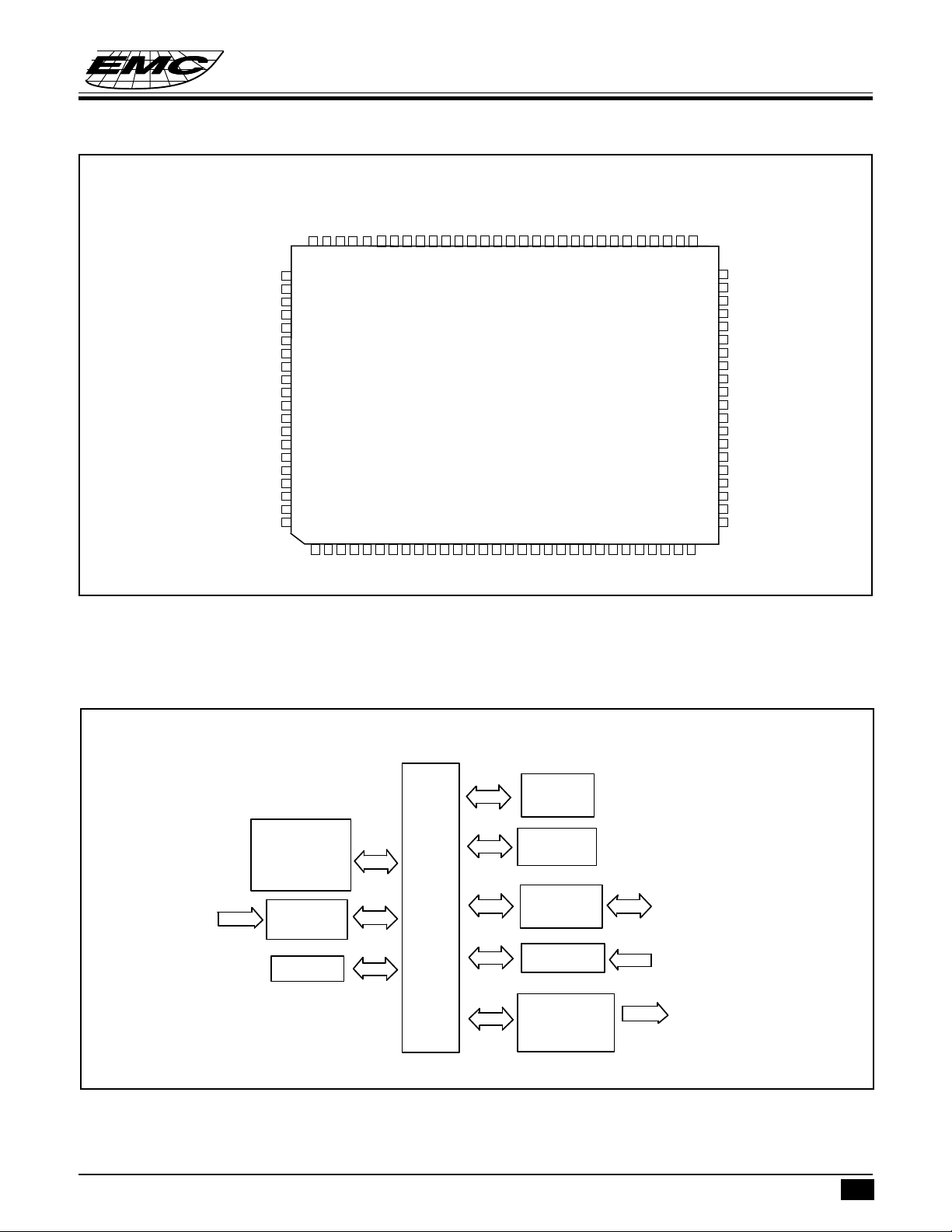
PIN ASSIGNMENTS
SEG41
SEG40
SEG39
SEG38
SEG37
SEG36
RESET
P7.7
P7.6
P7.5
P7.4
P7.3/INT3
P7.2/INT2
P7.1/INT1
P7.0/INT0
COM15/P6.7
COM14/P6.6
COM13/P6.5
COM12/P6.4
COM11/P6.3
COM10/P6.2
EM78860
8-BIT MICRO-CONTROLLER
COM9/P6.1
COM8/P6.0
COM7
COM6
COM5
COM4
COM3
GND
COM2
8079787776757473727170696867666564636261605958575655545352
SEG42
SEF43
TEST
SEG44/P8.0
SEG45/P8.1
SEG46/P8.2
SEG47/P8.3
SEG48/P8.4
SEG49/P8.5
SEG50/P8.6
SEG51/P8.7
SEG52/P9.0
SEG53/P9.1
SEG54/P9.2
SEG55/P9.3
SEG56/P9.4
SEG57/P9.5
SEG58/P9.6
SEG59/P9.7
VDD1
81
82
83
84
85
86
87
88
89
90
91
92
93
94
95
96
97
98
99
100
123456789
NC
NCNCNCNCNC
GND
PLLC
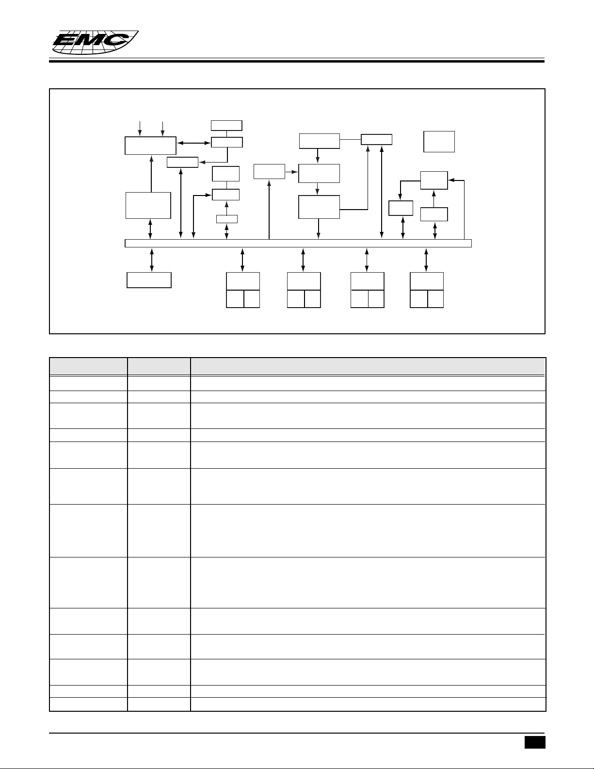
FUNCTIONAL BLOCK DIAGRAM
EM78860
101112131415161718192021222324252627282930
XIN
VDD
SEG0
SEG1
SEG2
SEG3
SEG4
SEG5
SEG6
SEG7
SEG8
XOUT
SEG9
SEG10
SEG11
SEG12
SEG13
SEG14
SEG15
VDD2
SEG16
51
50
49
48
47
46
45
44
43
42
41
40
39
38
37
36
35
34
33
32
31
SEG17
COM1
COM0
SEG35
SEG34
SEG33
SEG32
SEG31
SEG30
SEG29
SEG28
SEG27
SEG26
SEG25
SEG24
SEG23
SEG22
SEG21
SEG20
SEG19
SEG18
CPU
CLK
TIMING
CONTROL
TIMER
* This specification are subject to be changed without notice.
ROM
RAM
I/O PORT
INPUT PORT
LCD
LATCH
& DRIVER
I/O PORT
INPUT PORT
LCD
OUTPUT
6.24.1998
2
Page 3
EM78860
8-BIT MICRO-CONTROLLER
XIN XOUT
Oscillator/Timing
Control
Control of
sleep and
wake-up
on I/O ports
2.5K RAM
R1(TCC)
WDT Timer
Prescaler
GENERAL
RAM
RAM
R4
IOC6
Interrupt
Controller
DATA & CONTROL BUS
PORT6
R6
P60~P67
PORT7
IOC7
P70~P77
ROM
Instruction
register
Instruction
Decoder
R7
PORT8
IOC8
P80~P87
R2
R3
R5
R8
PORT9
IOC9
P90~P97
Stack
ALU
ACC
R9
PIN DESCRIPTIONS
Symbol Type Function
VDD POWER Power
GND POWER Gound
XTin I Input pin for 32.768 kHz oscillator
XTout O Output pin for 32.768 kHz oscillator
PLLC I Phase loop lock capacitor, connect a capacitor 0.01µ to 0.047µ with GND
COM0..COM7 O Common driver pins of LCD drivers
COM8..COM15 O (PORT6)
SEG0..SEG43 Segment driver pins of LCD drivers
SEG44..SEG51 O (PORT8)
SEG52..SEG59 O (PORT9) PORT9 AS FUNCTION KEY CAN WAKE UP WATCHDOG.
INT0 PORT7(0) PORT7(0)~PORT7(3) signal can be interrupt signals.
INT1 PORT7(1)
INT2 PORT7(2)
INT3 PORT7(3)
P7.0~P7.7 PORT7 PORT 7 can be INPUT or OUTPUT port each bit.
Internal Pull high function.
Key scan function.
Bit6,7 open drain function.
P6.0~P6.7 PORT6 PORT 6 can be INPUT or OUTPUT port each bit.
And shared with Common signal.
P8.0~P8.7 PORT8 PORT 8 can be INPUT or OUTPUT port each bit.
And shared with Common signal.
P9.0~P9.7 PORT9 PORT 9 can be INPUT or OUTPUT port each bit.
And shared with Common signal.
TEST I Test pin into test mode , normal low
RESET I
* This specification are subject to be changed without notice.
6.24.1998
3
Page 4
FUNCTION DESCRIPTION
Operational Registers
R0 (Indirect Addressing Register)
R0 is not a physically implemented register. It is useful as indirect addressing pointer. Any instruction using
R0 as register actually accesses data pointed by the RAM Select Register (R4).
R1 (TCC)
• Increased by an internal signal edge applied to TCC , or by the instruction cycle clock.
• Written and read by the program as any other register.
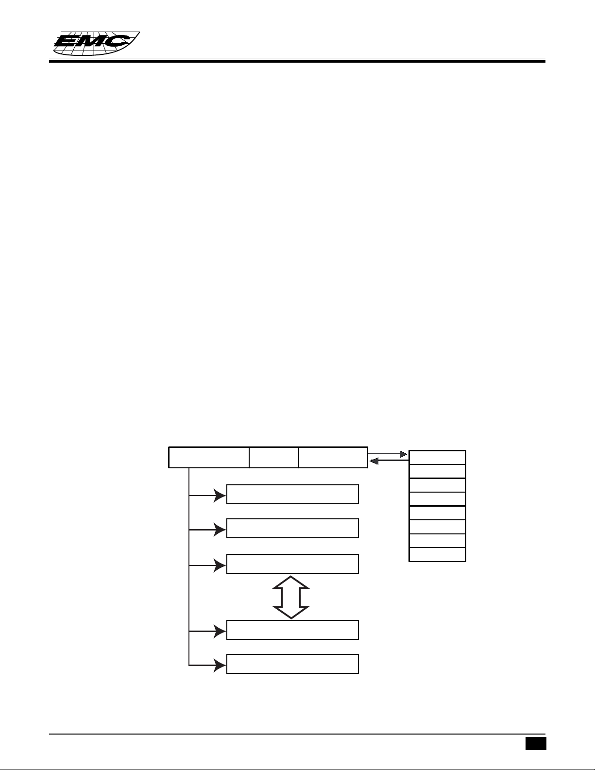
R2 (Program Counter)
• The structure is depicted in Fig. 4.
• Generates 16Kx13 on-chip ROM addresses to the relative programming instruction codes.
• ”JMP” instruction allows the direct loading of the low 10 program counter bits.
• “CALL” instruction loads the low 10 bits of the PC, PC+1, and then push into the stack..
• “RET’’ (“RETL k”, “RETI”) instruction loads the program counter with the contents at the top of stack.
• ”MOV R2,A” allows the loading of an address from the A register to the PC, and the ninth and tenth bits are
cleared to “0'’.
• “ADD R2,A” allows a relative address be added to the current PC, and contents of the ninth and tenth bits are
cleared to “0'’.
• “TBL” allows a relative address be added to the current PC, and contents of the ninth and tenth bits don’t
change.
• The most significant bit (A10~A13) will be loaded with the content ofbit PS0~PS3 in the status register (R5)
upon the execution of a “JMP’’, “CALL’’, “ADD R2,A’’, or “MOV R2,A’’ instruction.
EM78860
8-BIT MICRO-CONTROLLER
A13 A12 A11 A10 A9 A8
PC
Fig.4 Program counter organization
A7~A0 Stack 1
0000 PAGE0 0000~03FF
0000 PAGE1 0400~07FF
0000 PAGE3 0800~0BFF
1110 PAGE14 3800~3BFF
1111 PAGE15 3C00~3FFF
CALL
RET
RETTL
RETI
Stack 2
Stack 3
Stack 4
Stack 5
Stack 6
Stack 7
Stack 8
* This specification are subject to be changed without notice.
6.24.1998
4
Page 5
ADDRESS REGISTER
R0
00
R1(TCC)
01
R2(PC)
02
R3(STATUS)
03
R4(RSR)
04
R5(ROM PAGE)
05
06
R6(PORT6)
07
R7(PORT7)
08
R8(PORT8)
09
R9(PORT9)
0A
RA(CLK)
0B
RB()
0C
RC(2.5K RAM ADRESS)
0D
RD(2.5K RAM DATA)
0E
RE
0F
RF(INT FLAG)
10
:
1F
16x8
Common
Register
CONTROL REGISTER
(PAGE0)
page0
IOC6
IOC7
IOC8
IOC9
IOCA
IOCB(LCD ADDRESS)
IOCC(LCD DATA)
IOCD(PULL HIGH)
IOCE(IO, LCD)
IOCF(INT CONTROL)
RC(ADDRESS) RD(DATA)
EM78860
8-BIT MICRO-CONTROLLER
CONTROL REGISTER
(PAGE1)
page1
IOCB(COUNTER1)
IOCC(COUNTER2)
20
:
3F
BANK0~BANK3
32X8 ~ 32X8
REGISTER
255
0
:
BAND1
256X8
BAND1
256X8
. . . . . . . . . . . .
. . . . . . . . . . . .
BAND10
256X8
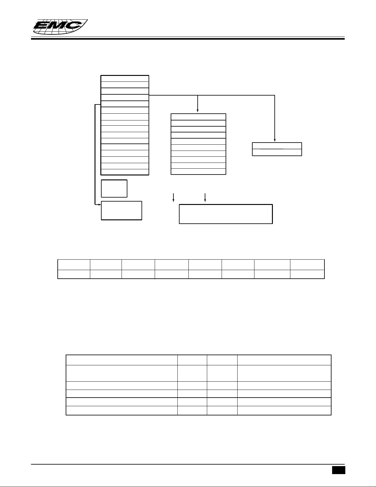
Fig.5 Data memory configuration
R3 ( Status Register )
76543210
- PAGE - T P Z DC C
• Bit 0 (C) : Carry flag
• Bit 1 (DC) : Auxiliary carry flag
• Bit 2 (Z) : Zero flag
• Bit 3 (P) : Power down bit. Set to 1 during power on or by a “WDTC” command and reset to 0 by a
“SLEP” command.
• Bit 4 (T) : Time-out bit. Set to 1 by the “SLEP” and “WDTC” command, or during power up and reset
to 0 by WDT time out.
EVENT T P REMARK
WDT TIME OUT 0 0
sleep mode
WDT time out (not sleep mode 0 1
/RESET wake up from sleep 1 0
power up 1 1
Low pulse on /RESET x x x . . don't care
• Bit 5 : unused
• Bit 6 PAGE : changed IOCB~IOCE to another page, 0/1→page0/page1
• Bit 7 unused
* This specification are subject to be changed without notice.
6.24.1998
5
Page 6
8-BIT MICRO-CONTROLLER
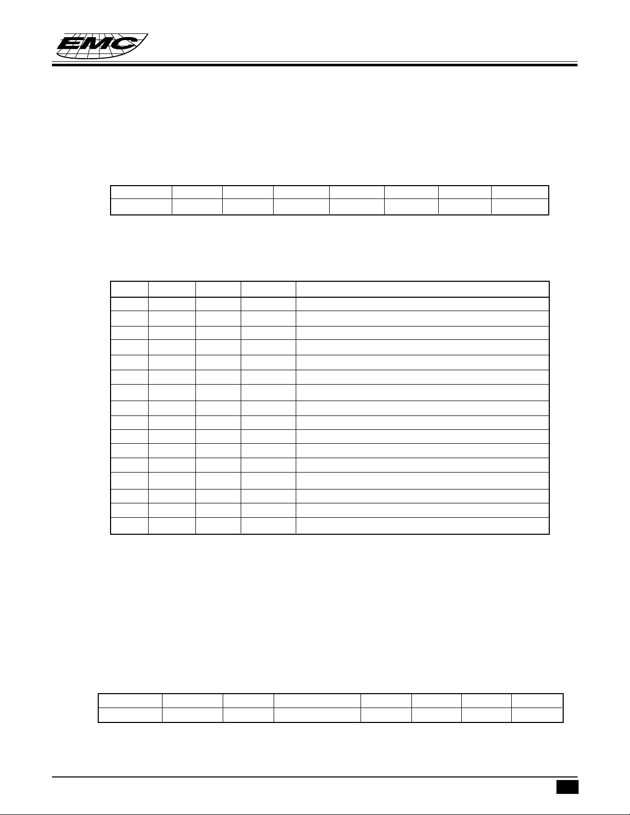
R4 ( RAM Select Register )
• Bit 0 ~ 5 are used to select up to 64 register in the indirect addressing mode.
• Bit 6 ~ 7 determine which bank is actived among the 4 banks.
• See the configuration of the data memory in Fig.4.
R5 ( Program Page Select Register)
765 43210
- - - - PS3 PS2 PS1 PS0
• Bit 0 (pS0) ~ 3 (PS3) Page selec bits.
Page select bits
PS3 PS2 PS1 PS0 program memory page (Address)
0000 Page 0
0001 Page 1
0010 Page 2
0011 Page 3
0100 Page 4
0101 page 5
0110 Page 6
0111 Page 7
1000 Page 8
1001 Page 9
1010 Page 10
1011 Page 11
1100 Page 12
1101 Page 13
1110 Page 14
1111 Page 15
EM78860
• User can use PAGE instruction to change page. To maintain program page by user. Otherwise, user can use
far jump (FJMP) or far call (FCALL) instructions to program user's code. And the program page is maintained
by EMC's complier. It will change user's program by inserting instruction within program.
• Bit4~7 : unused
R6 ~R9 ( Port 6 ~ Port 9)
• Five 8-bit I/O registers.
RA
7654 3210
IDLE /358E /LPD /LOW-BAT 0 0 0 0
• Bit0 ~ Bit3 unused, please set to "0"
* This specification are subject to be changed without notice.
6.24.1998
6
Page 7
EM78860
t
8-BIT MICRO-CONTROLLER
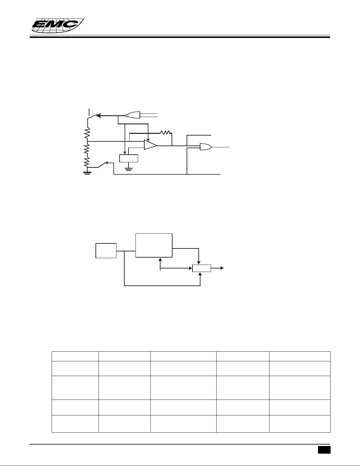
• Bit4(Read Only)(Low battery signal) 0/1 = Battery voltage is low/Normal .
If the battery voltage is under 3.6V then sends a ‘0’ signal to RA register bit4 or a ‘1’ signal to this Bit if VDD
is over 3.8V.
• Bit5(read/Write)(Low battery detect enable)
0/1 = low battery detect DISABLE/ENABLE.
The relation between /LPD,/POVD and /LOW_BAT can see Fig6.
Vdd
/POVD
s2
1 on
0 off
1 on
Vref
/LPD
1 on
+
-
to Low bat
To rese
s2
1 on
0 off
/LPD
Fig6. The relation between /LPD,/POVD
• Bit6(read/write)(PLL enable signal)
0/1=DISABLE/ENABLE
The relation between 32.768K and 3.679M can see Fig7.
PLL
32.768K
3.679M
/358E
switch
1
To system clock
0
Fig7. The relation between 32.768K and 3.679K .
• Bit7 IDLE: sleep mode selection bit
0/1=sleep mode/IDLE mode. This bit will decide SLEP instruction which mode to go.
These IDLE mode can be waken up by TCC clock or Watch Dog or PORT9 and run from “SLEP” next
instruction.
These SLEEP mode can be waken up by Watch Dog or PORT9 and run from address “00”.
SLEEP mode IDLE mode GREEN mode NORMAL mode
RA(7,6)=(0,0) RA(7,6)=(1,0) RA(7,6)=(x,0) RA(7,6)=(x,1)
+ SLEP + SLEP no SLEP no SLEP
TCC time out X Wake-up Interrupt Interrupt
+ Interrupt
+ Next instruction
WDT time out RESET Wake-up RESET RESET
+ Next instruction RESET RESET
Port9 wake-up RESET Wake-up
+ Next instruction
* This specification are subject to be changed without notice.
6.24.1998
7
Page 8
8-BIT MICRO-CONTROLLER
RB
Empty register, please don't use.
RC(2.5k RAM address)(read/write)
76 5 4 3 2 1 0
CIDA7 CIDA6 CIDA5 CIDA4 CIDA3 CIDA2 CIDA1 CIDA0
• Bit 0 ~ Bit 7 select CALLER ID RAM address up to 256.
RD(2.5k RAM address)(read/write)
• Bit 0 ~ Bit 8 are CALLER ID RAM data transfer register.
User can see IOCA register how to select CID RAM banks.
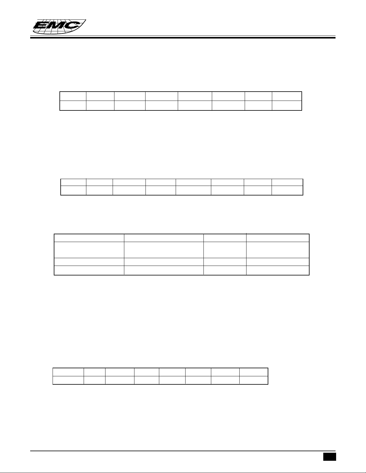
RE(LCD Driver,WDT Control)(read/write)
76 5 4 3 2 1 0
- /WDTE /WUP9H /WUP9L /WURING LCD_C2 LCD_1 LCD_M
EM78860
• Bit0 (LCD_M):LCD_M decides the methods, including duty, bias, and frame frequency.
• Bit1~Bit2 (LCD_C#):LCD_C# decides the LCD display enable or blanking. change the display duty must
set the “LCD_C2,LCD_C1” to “00”.
LCD_C2,LCD_C1 LCD Display Control LCD_M duty bias
0 0 Change duty 0 1/16 1/4
Disable(turn off LCD) 1 1/8 1/4
0 1 Blanking : :
1 1 LCD display enable : :
• Bit3 unused. Please set to "0"
• Bit4(/WUP9L, PORT9 low nibble Wake Up Enable) : used to enable the wake-up function of low nibble in
PORT9, (1/0=enable/disable)
• Bit5 (/WUP9H, PORT9 high nibble WAKE Up Enable) : used to enable the wake-up function of high
nibble in PORT9, (1/0=enable/disable)
• Bit6 (/WDTE, Watch Dog Timer Enable)
Control bit used to enable Watchdog timer. (1/0=enable/disable)
• Bit7 unused
RF (Interrupt Status Register)
765432 1 0
INT3 - C8_2 C8_1 INT2 INT1 INT0 TCIF
• “1” means interrupt request, “0” means non-interrupt
• Bit 0 (TCIF) TCC timer overflow interrupt flag. Set when TCC timer overflows .
• Bit 1 (INT0) external INT0 pin interrupt flag .
• Bit 2 (INT1) external INT1 pin interrupt flag .
• Bit 3 (INT2) external INT2 pin interrupt flag .
• Bit 4 (C8_1) internal 8 bit counter interrupt flag .
• Bit 5 (C8_2) internal 8 bit counter interrupt flag .
* This specification are subject to be changed without notice.
6.24.1998
8
Page 9
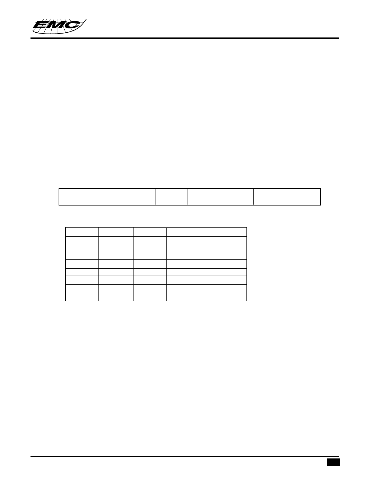
• Bit 6 :unused. Please set to ‘0’.
• Bit 7 (INT3) external INT3 pin interrupt flag.
• High to low edge trigger , Refer to the Interrupt subsection.
• IOCF is the interrupt mask register. User can read and clear.
R10~R3F (General Purpose Register)
• R10~R3F (Banks 0~3) all are general purpose registers.
Special Purpose Registers
A (Accumulator)
• Internal data transfer, or instruction operand holding
• It’s not an addressable register.
CONT (Control Register)
76543210
- INT TS - PAB PSR2 PSR1 PSR0
EM78860
8-BIT MICRO-CONTROLLER
• Bit 0 (PSR0) ~ Bit 2 (PSR2) TCC/WDT prescaler bits.
PSR2 PSR1 PSR0 TCC Rate WDT Rate
0 0 0 1:2 1:1
0 0 1 1:4 1:2
0 1 0 1:8 1:4
0 1 1 1:16 1:8
1 0 0 1:32 1:16
1 0 1 1:64 1:32
1 1 0 1:128 1:64
1 1 1 1:256 1:128
• Bit 3 ( PAB ) Prescaler assignment bit
0/1: TCC/WDT
• Bit 4 unused
• Bit 5 ( TS ) : TCC signal source
0 : internal instruction cycle clock
1 : 16.38KHz
• Bit 6 : (INT)INT enable flag
0: interrupt masked by DISI or hardware interrupt
1: interrupt enabled by ENI/RETI instructions
• Bit 7 : unused
• CONT register is readable and writable.
* This specification are subject to be changed without notice.
6.24.1998
9
Page 10
EM78860
8-BIT MICRO-CONTROLLER
IOC6 ~ IOC9 ( I/O Port Control Register )
• Five I/O direction control registers.
• “1” put the relative I/O pin into high impedance, while “0” put the relative I/O pin as output.
• User can see IOCB register how to switch to normal I/O port.
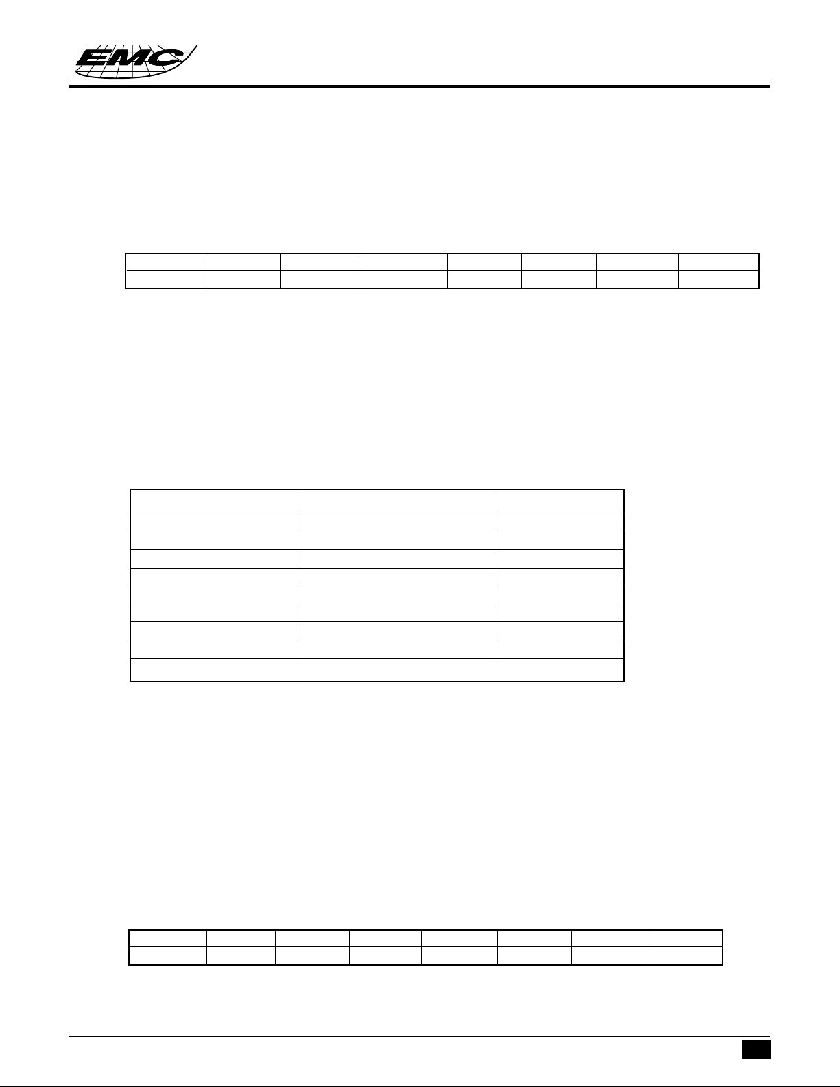
IOCA (RAM,IO ,PAGE Control Register)(read/write,initial “00000000”)
765 432 1 0
P8SH P8SL 0 CALL_4 CALL_3 CALL_2 CALL_1 0
• Bit0 unused
• Bit4~Bit1:”000" to “1001” are ten blocks of RAM area. User can use 2.5K RAM with RC ram address.
• Bit 5 unused
• Bit6: port8 low nibble switch, 0/1= normal I/O port/SEGMENT output .
• Bit7: port8 high nibble switch , 0/1= normal I/O port/SEGMENT output
IOCB (LCD ADDRESS)
PAGE0 : Bit6 ~ Bit0 = LCDA6 ~ LCDA0
The LCD display data is stored in the data RAM . The relation of data area and COM/SEG pin is as below:
COM15 ~ COM8 COM7 ~ COM0
40H (Bit15 ~ Bit8) 00H (Bit7 ~ Bit0) SEG0
41H 01H SEG1
:: :
:: :
7BH 3BH SEG59
7CH 3CH Empty
7DH 3DH Empty
7EH 3EH Empty
7FH 3FH Empty
PAGE1 : 8 bit up-counter (COUNTER1) preset and read out register . ( write = preset ) . After a interruption
, it will count from “00”.
IOCC (LCD DATA)
PAGE0 : Bit7 ~ Bit0 = LCD RAM data register
PAGE1 : 8 bit up-counter (COUNTER2) preset and read out register. (write=preset) After a interruption, it will
count from "00".
IOCD (Pull-high Control Register)
7654 32 10
PH7 PH6 PH5 PH4 PH3 PH2 PH1 PH0
• Bit 0 ~ 7 (/PH#) Control bit used to enable the pull-high of PORT7(#) pin.
1: Enable internal pull-high
0: Disable internal pull-high
* This specification are subject to be changed without notice.
6.24.1998
10
Page 11
EM78860
8-BIT MICRO-CONTROLLER
7654 32 10
P9SH P9SL P6S Bias3 Bias2 Bias1 0 SC
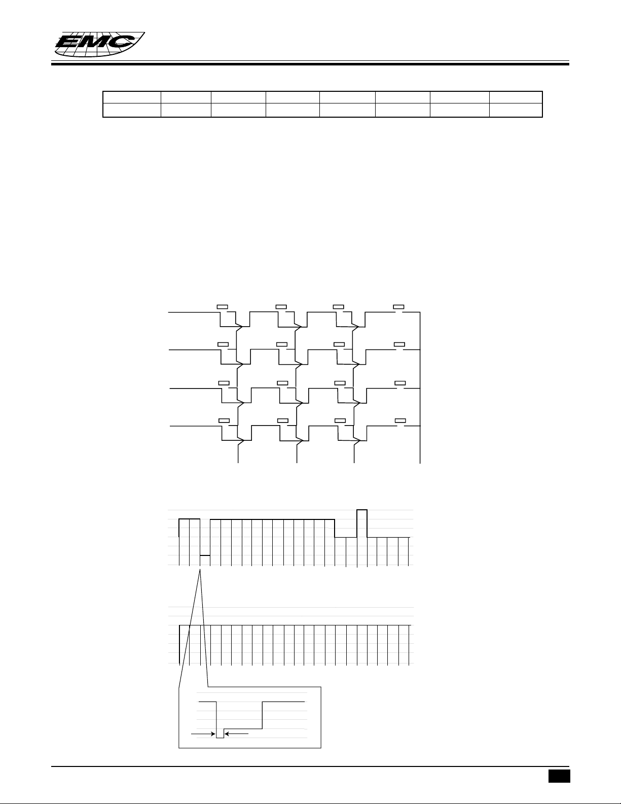
• Bit 0 :SC (SCAN KEY signal ) 0/1 = disable/enable. Once you enable this bit , all of the LCD signal will have
a low pulse during a common period. This pulse has 30us width. Please use the procedure to implement the
key scan function.
a. set port7 as input port
b. set IOCD page0 port7 pull high
c. enable scan key signal
d. Once push a key . Set RA(6)=1 and switch to normal mode.
e. Blank LCD. Disable scan key signal.
f. Set P6S =0. Port6 sent probe signal to port7 and read port7. Get the key.
g. Note!! A probe signal should be delay a instruction at least to another probe signal.
h. Set P6S =1. Port6 as LCD signal. Enable LCD.
P63
P62
P61
P60
com2
KEY5
KEY1
KEY2
KEY3
KEY4
P73 P72 P71 P70
Fig.8. Key scan circuit
VDD
V1
V2
V3
V4
VLCD
GND
seg
30µs
Fig.9. Key scan signal
* This specification are subject to be changed without notice.
VDD
V1
V2
V3
V4
VLCD
GND
6.24.1998
11
Page 12
EM78860
8-BIT MICRO-CONTROLLER
• Bit 1 : zero
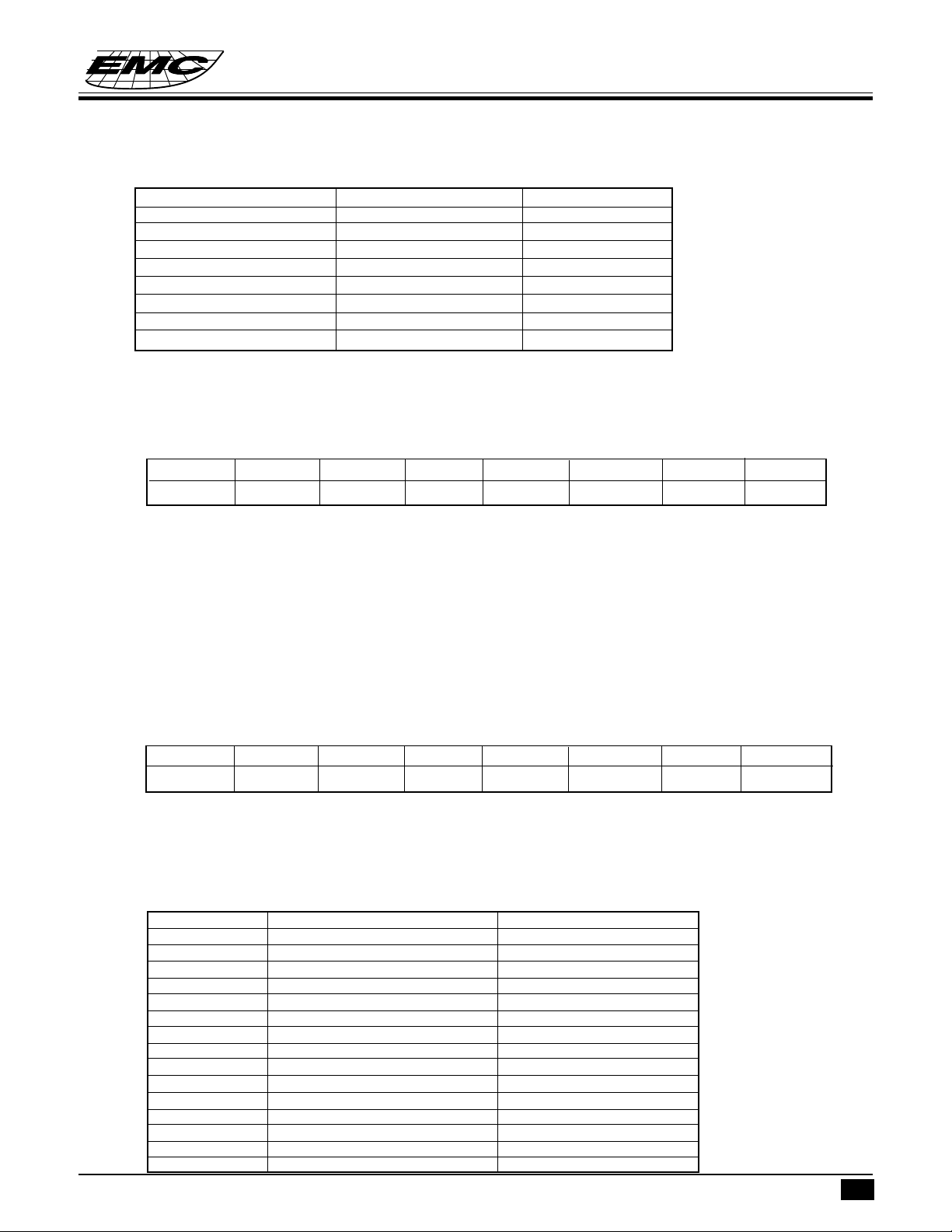
• Bit 2~4 (Bias1~Bias3) Control bits used to choose LCD operation voltage .
LCD operate voltage Vop (VDD 5V) VDD=5V
000 0.60VDD 3.0V
001 0.66VDD 3.3V
010 0.74VDD 3.7V
011 0.82VDD 4.0V
100 0.87VDD 4.4V
101 0.93VDD 4.7V
110 0.96VDD 4.8V
111 1.00VDD 5.0V
• Bit5:port6 switch , 0/1= normal I/O port/COMMON output
• Bit6:port9 low nibble switch , 0/1= normal I/O port/SEGMENT output . Bit7:port9 high nibble switch
PAGE1 :
7654321 0
OP77 OP76 C2S C1S PSC1 PSC0 - -
• Bit0: unused, please set to ‘0’
• Bit1: unused, please set to ‘0‘
• Bit3~Bit2: counter1 prescaler , reset=(0,0)
(PSC1,PSC0) = (0,0)=>1:1 , (0,1)=>1:2 , (1,0)=>1:4 , (1,1)=>1:8
• Bit4:counter1 source , (0/1)=(32768Hz/3.679MHz if enable)
• Bit5:counter2 source , (0/1)=(32768Hz/3.679MHz if enable) scale=1:1
• Bit6:P76 opendrain control (0/1)=(disable/enable)
• Bit7:P77 opendrain control (0/1)=(disable/enable)
IOCF (Interrupt Mask Register)
7654321 0
INT3 - C8_2 C8_1 INT2 INT1 INT0 TCIF
• Bit 0 ~ 7 interrupt enable bit.
0: disable interrupt
1: enable interrupt
• IOCF Register is readable and writable.
It is very important to save ACC,R3 and R5 when processing a interruption.
Address Instruction Note
0x08 DISI ;Disable interrupt
0x09 MOV A_BUFFER,A ;Save ACC
0x0A SWAP A_BUFFER
0x0B SWAPA 0x03 ;Save R3 status
0x0C MOV R3_BUFFER,A
0x0D MOV A,0x05 ;Save ROM page register
0x0E MOV R5_BUFFER,A
::
::
: MOV A,R5_BUFFER ;Return R5
: MOV 0X05,A
: SWAPA R3_BUFFER ;Return R3
: MOV 0X03,A
: SWAPA A_BUFFER ;Return ACC
: RETI
* This specification are subject to be changed without notice.
6.24.1998
12
Page 13
EM78860
8-BIT MICRO-CONTROLLER
TCC/WDT Prescaler
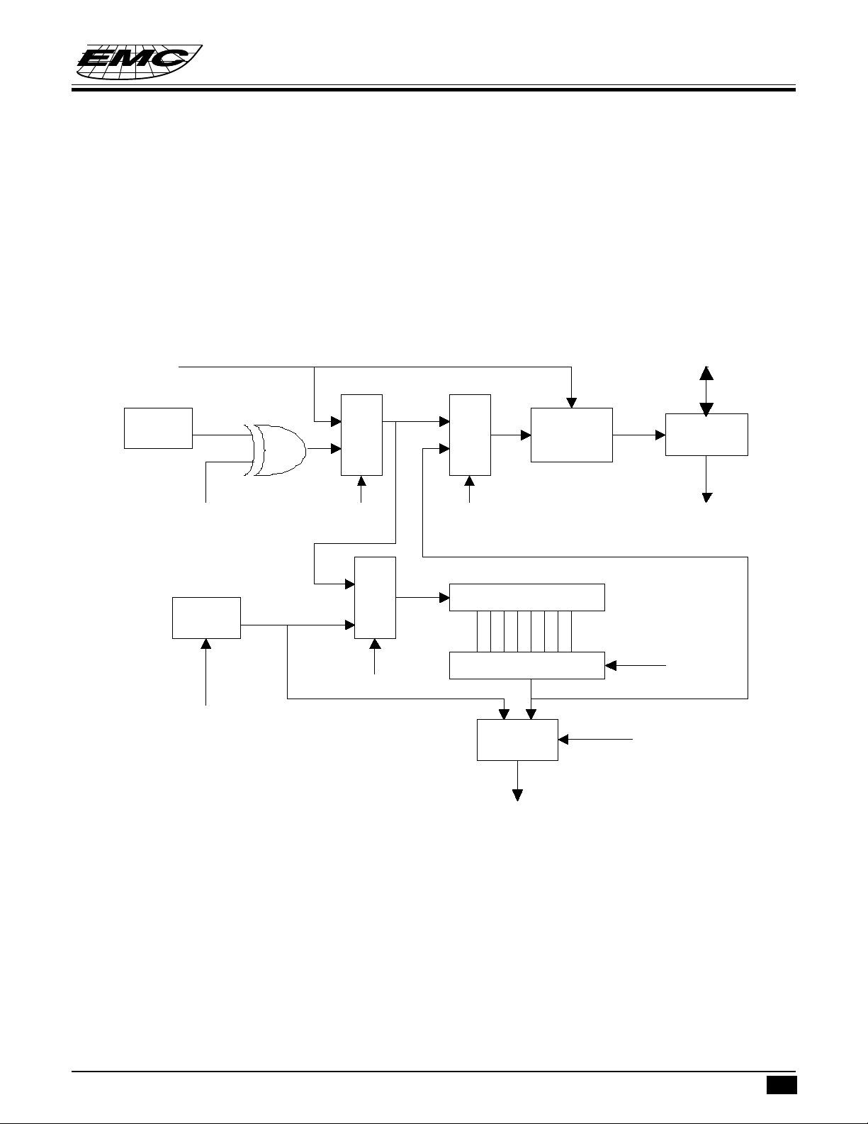
There is an 8-bit counter available as prescaler for the TCC or WDT. The prescaler is available for the TCC
only or WDT only at the same time.
• An 8 bit counter is available for TCC or WDT determined by the status of the bit 3 (PAB) of the CONT
register.
• See the prescaler ratio in CONT register.
• Fig. 10 depicts the circuit diagram of TCC/WDT.
• Both TCC and prescaler will be cleared by instructions which write to TCC each time.
• The prescaler will be cleared by the WDTC and SLEP instructions, when assigned to WDT mode.
• The prescaler will not be cleared by SLEP instructions, when assigned to TCC mode.
TCC
(32K CLK)
CLK(=Fosc/2)
TE
WDT
WDTE
Data Bus
0
M
1
U
X
TS
0
M
U
X
1
PAB
1
0
M
U
X
PAB
8-bit Counter
8-to-1 MUX
MUX
SYNC
2 cycle
TCC(R1)
TCC overflow interrupt
PSR0~PSR2
PAB
Fig. 10 Block diagram of TCC WDT
I/O Ports
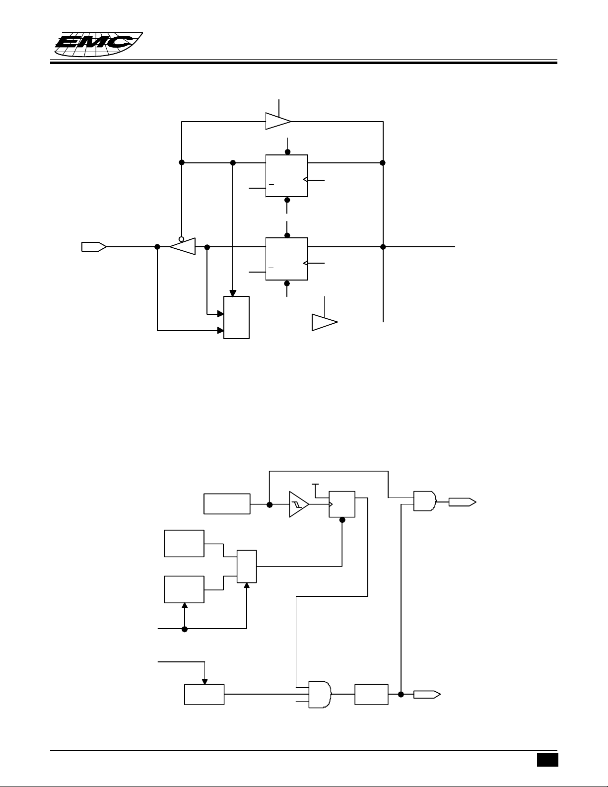
The I/O registers, Port 6 ~ Port 9, are bi-directional tri-state I/O ports. Port 7 can be pulled-high internally by
software control. The I/O ports can be defined as “input” or “output” pins by the I/O control registers (IOC6 ~
IOC9 ) under program control. The I/O registers and I/O control registers are both readable and writable. The
I/O interface circuit is shown in Fig.11.
* This specification are subject to be changed without notice.
WDT timeout
6.24.1998
13
Page 14
PORT
EM78860
8-BIT MICRO-CONTROLLER
PCRD
PR
CLK
CL
PR
CLK
CL
D
D
PCWR
IOD
PDWR
PDRD
Q
Q
Q
Q
0
M
U
1
X
Fig. 11 The circuit of I/O port and I/O control register
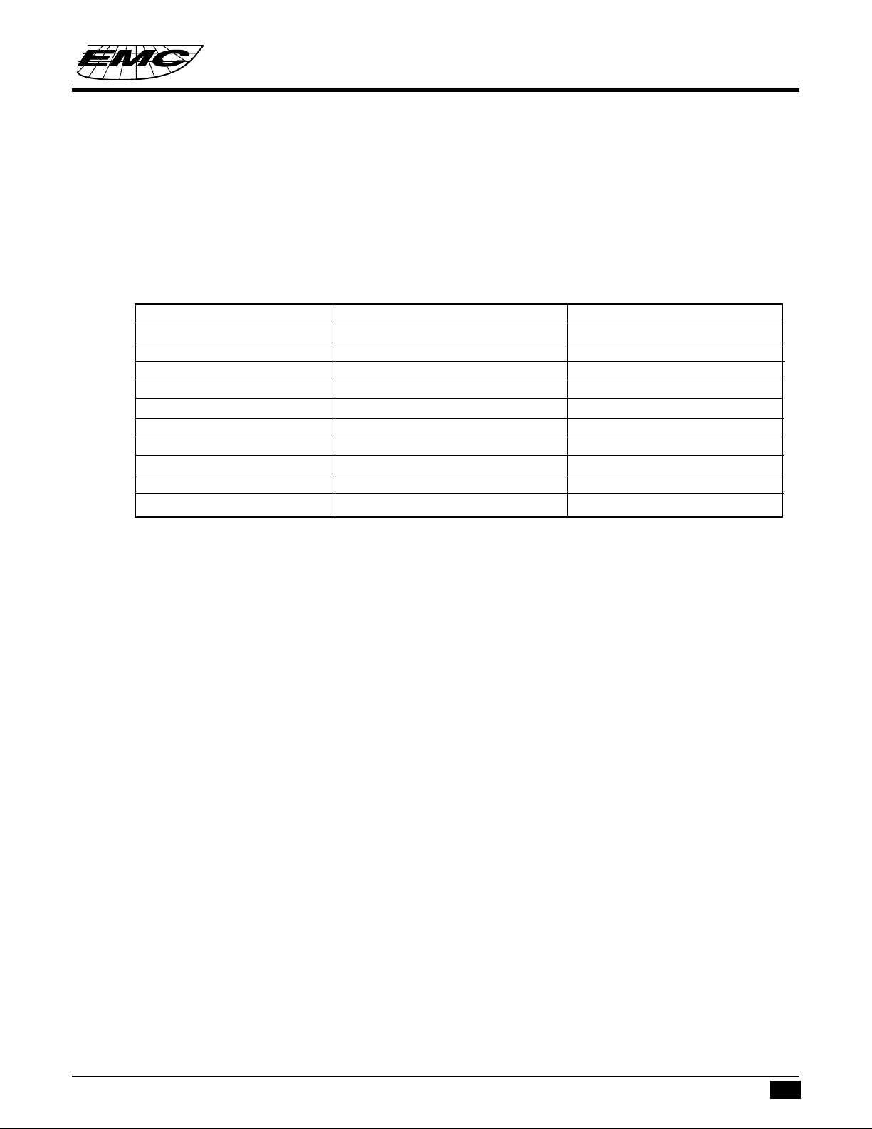
RESET and Wake-up
The RESET can be caused by
(1) Power on reset, or Voltage detector
(2) WDT timeout. (if enabled and in GREEN or NORMAL mode)
Note that only Power on reset, or only Voltage detector in Case(1) is enabled in the system by CODE Option bit.
If Voltage detector is disabled, Power on reset is selected in Case (1). Refer to Fig. 12.
V
DD
Code
Option
Power-on
Reset
Voltage
Detector
/Enable
Oscillator
1
0
DQ
CLK
CLR
M
U
X
CLK
WDTE
WDT timeout
WDT
Fig. 12 Block diagram of Reset of controller
* This specification are subject to be changed without notice.
18 ms
RESET
6.24.1998
14
Page 15
8-BIT MICRO-CONTROLLER
Once the RESET occurs, the following functions are performed.
• The oscillator is running, or will be started.
• The Program Counter (R2) is set to all “0”.
• When power on, the upper 3 bits of R3 and the upper 2 bits of R4 are cleared.
• The Watchdog timer and prescaler are cleared.
• The Watchdog timer is disabled.
• The CONT register is set to all “1”
• The other register (bit7..bit0)
R5 = “00000000”
R6 = PORT IOC6 = “11111111”
R7 = PORT IOC7 = “11111111”
R8 = PORT IOC8 = “11111111”
R9 = PORT IOC9 = “11111111”
RA = “010x0xxx IOCA = “00000000”
RB = “11111111” Page0 IOCB = “00000000” Page1 IOCB = “00000000”
RC = “00000000” Page0 IOCC = “0xxxxxxx” Page1 IOCC = “00000000”
RD = “xxxxxxxx” Page0 IOCD = “00000000”
RE = “00000000” Page0 IOCE = “00000000” Page1 IOCE = “00000000”
RF = “00000000” IOCF = “00000000”
EM78860
The controller can be awakened from SLEEP mode or IDLE mode (execution of “SLEP” instruction, named as
SLEEP MODE or IDLE mode) by (1)TCC time out (IDLE mode only) (2) WDT time-out (if enabled) or, (3)
external input at PORT9 . The three cases will cause the controller wake up and run from next instruction in IDLE
mode , reset in SLEEP mode . After wake-up , user should control WATCH DOG in case of reset in GREEN
mode or NORMAL mode. The last two should be open RE register before into SLEEP mode or IDLE mode .
The first one case will set a flag in RF bit0 . And it will go to address 0x08 when TCC generate a interrupt .
Interrupt
The chip has internal interrupts which are falling edge triggered, as followed : TCC timer overflow interrupt
(internal) , two 8-bit counters overflow interrupt .
If these interrupt sources change signal from high to low , then RF register will generate ‘1’ flag to corresponding
register if you enable IOCF register.
RF is the interrupt status register which records the interrupt request in flag bit. IOCF is the interrupt mask
register. Global interrupt is enabled by ENI instruction and is disabled by DISI instruction. When one of the
interrupts (when enabled) generated, will cause the next instruction to be fetched from address 008H. Once in
the interrupt service routine the source of the interrupt can be determined by polling the flag bits in the RF register.
The interrupt flag bit must be cleared in software before leaving the interrupt service routine and enabling
interrupts to avoid recursive interrupts.
There are four external interrupt pins including INT0 , INT1 , INT2 , INT3 . And four internal counter interrupt
available.
External interrupt INT0 , INT1 , INT2 , INT3 signals are from PORT7 bit0 to bit3 . If IOCF is enable then these
signal will cause interrupt , or these signals will be treated as general input data .
After reset, the next instruction will be fetched from address 000H and the instruction inturrept is 001H and the
hardware inturrept is 008H.
TCC will go to address 0x08 in GREEN mode or NORMAL mode after time out. And it will run next
instruction from “SLEP” instruction and then go to address 0x08 in IDLE mode . These three cases will
set a RF flag.
* This specification are subject to be changed without notice.
6.24.1998
15
Page 16
8-BIT MICRO-CONTROLLER
It is very important to save ACC,R3 and R5 when processing a interruption.
Address Instruction Note
0x08 DISI ;Disable interrupt
0x09 MOV A_BUFFER,A ;Save ACC
0x0A SWAP A_BUFFER
0x0B SWAPA 0x03 ;Save R3 status
0x0C MOV R3_BUFFER,A
0x0D MOV A,0x05 ;Save ROM page register
0x0E MOV R5_BUFFER,A
::
::
: MOV A,R5_BUFFER ;Return R5
: MOV 0X05,A
: SWAPA R3_BUFFER ;Return R3
: MOV 0X03,A
: SWAPA A_BUFFER ;Return ACC
: RETI
EM78860
Instruction Set
Instruction set has the following features:
(1). Every bit of any register can be set, cleared, or tested directly.
(2). The I/O register can be regarded as general register. That is, the same instruction can operates on I/O register.
The symbol “R” represents a register designator which specifies which one of the 64 registers (including
operational registers and general purpose registers) is to be utilized by the instruction. Bits 6 and 7 in R4
determine the selected register bank. “b’’ represents a bit field designator which selects the number of the
bit, located in the register “R’’, affected by the operation. “k’’ represents an 8 or 10-bit constant or literal
value.
INSTRUCTION BINARY HEX MNEMONIC OPERATION STATUS
AFFECTED
0 0000 0000 0000 0000 NOP No Operation None
0 0000 0000 0001 0001 DAA Decimal Adjust A C
0 0000 0000 0010 0002 CONTW A CONT None
0 0000 0000 0011 0003 SLEP 0 WDT, Stop oscillator T,P
0 0000 0000 0100 0004 WDTC 0 WDT T,P
0 0000 0000 rrrr 000r IOW R A IOCR None
0 0000 0001 0000 0010 ENI Enable Interrupt None
0 0000 0001 0001 0011 DISI Disable Interrupt None
0 0000 0001 0010 0012 RET [Top of Stack] PC None
0 0000 0001 0011 0013 RETI [Top of Stack] PC
Enable Interrupt None
0 0000 0001 0100 0014 CONTR CONT A None
0 0000 0001 rrrr 001r IOR R IOCR A None
0 0000 0010 0000 0020 TBL R2+A R2 bits 9,10 do not clear Z,C,DC
0 0000 01rr rrrr 00rr MOV R,A A R None
0 0000 1000 0000 0080 CLRA 0 A Z
0 0000 11rr rrrr 00rr CLR R 0 R Z
0 0001 00rr rrrr 01rr SUB A,R R-A A Z,C,DC
0 0001 01rr rrrr 01rr SUB R,A R-A R Z,C,DC
* This specification are subject to be changed without notice.
6.24.1998
16
Page 17
EM78860
8-BIT MICRO-CONTROLLER
INSTRUCTION BINARY HEX MNEMONIC OPERATION STATUS
AFFECTED
0 0001 10rr rrrr 01rr DECA R R-1→AZ
0 0001 11rr rrrr 01rr DEC R R-1→RZ
0 0010 00rr rrrr 02rr OR A,R A∨R→AZ
0 0010 01rr rrrr 02rr OR R,A A∨R→RZ
0 0010 10rr rrrr 02rr AND A,R A & R→AZ
0 0010 11rr rrrr 02rr AND R,A A & R→RZ
0 0011 00rr rrrr 03rr XOR A,R A⊕R→AZ
0 0011 01rr rrrr 03rr XOR R,A A⊕R→RZ
0 0011 10rr rrrr 03rr ADD A,R A + R→A Z,C,DC
0 0011 11rr rrrr 03rr ADD R,A A + R→R Z,C,DC
0 0100 00rr rrrr 04rr MOV A,R R→AZ
0 0100 01rr rrrr 04rr MOV R,R R→RZ
0 0100 10rr rrrr 04rr COMA R /R→AZ
0 0100 11rr rrrr 04rr COM R /R→RZ
0 0101 00rr rrrr 05rr INCA R R+1→AZ
0 0101 01rr rrrr 05rr INC R R+1→RZ
0 0101 10rr rrrr 05rr DJZA R R-1→A, skip if zero None
0 0101 11rr rrrr 05rr DJZ R R-1→R, skip if zero None
0 0110 00rr rrrr 06rr RRCA R R(n)→A(n-1)
R(0)→C, C→A(7) C
0 0110 01rr rrrr 06rr RRC R R(n)→R(n-1)
R(0)→C, C→R(7) C
0 0110 10rr rrrr 06rr RLCA R R(n)→A(n+1)
R(7)→C, C→A(0) C
0 0110 11rr rrrr 06rr RLC R R(n)→R(n+1)
R(7) →C, C→R(0) C
0 0111 00rr rrrr 07rr SWAPA R R(0-3)→A(4-7)
R(4-7)→A(0-3) None
0 0111 01rr rrrr 07rr SWAP R R(0-3)↔R(4-7) None
0 0111 10rr rrrr 07rr JZA R R+1→A, skip if zero None
0 0111 11rr rrrr 07rr JZ R R+1→R, skip if zero None
0 100b bbrr rrrr 0xxx BC R,b 0→R(b) None
0 101b bbrr rrrr 0xxx BS R,b 1→R(b) None
0 110b bbrr rrrr 0xxx JBC R,b if R(b)=0, skip None
0 111b bbrr rrrr 0xxx JBS R,b if R(b)=1, skip None
1 00kk kkkk kkkk 1kkk CALL k PC+1→[SP]
(Page, k)→PC None
1 01kk kkkk kkkk 1kkk JMP k (Page, k)→PC None
1 1000 kkkk kkkk 18kk MOV A,k k→A None
1 1001 kkkk kkkk 19kk OR A,k A k→AZ
1 1010 kkkk kkkk 1Akk AND A,k A & k→AZ
1 1011 kkkk kkkk 1Bkk XOR A,k A k→AZ
1 1100 kkkk kkkk 1Ckk RETL k k→A, [Top of Stack]→PC None
1 1101 kkkk kkkk 1Dkk SUB A,k k-A→A Z,C,DC
1 1110 0000 0001 1E01 INT PC+1→[SP]
001H→PC None
1 1110 1000 kkkk 1E8k PAGE k K->R5 None
1 1111 kkkk kkkk 1Fkk ADD A,k k+A→A Z,C,DC
* This specification are subject to be changed without notice.
6.24.1998
17
Page 18
EM78860
8-BIT MICRO-CONTROLLER
CODE Option Register
The chip has one CODE option register which is not part of the normal program memory. The option bits
cannot be accessed during normal program execution.
76543210
------/POVD -
• Bit 0 : unsed
• Bit 1 ( /POVD ) : Power on voltage detector.
0 : enable
1 : disable
/POVD 1.8V reset power on 3.6V detect no 3.6V detect control sleep mode
reset reset by RA(5) current
1 no yes yes yes 1µA
0 yes yes yes yes 15µA
• Bit 2~7 : unused, must be "0"s.
LCD Driver
The chip can drive LCD directly and has 60 segments and 16 commons that can drive 60*16 dots totally. LCD
block is made up of LCD driver , display RAM, segment output pins , common output pins and LCD operating
power supply pins.
Duty , bias , the number of segment , the number of common and frame frequency are determined by LCD mode
register . LCD control register.
The basic structure contains a timing control which uses the basic frequency 32.768KHz to generate the proper
timing for different duty and display access. RE register is a command register for LCD driver, the LCD display
( disable, enable, blanking) is controlled by LCD_C and the driving duty and bias is decided by LCD_M and the
display data is stored in data RAM which address and data access controlled by registers RC and RD.
32.768KHz
RC(address)
LCD timing control
RE(LCD_C,LCD_M)
LCD duty control
RD(data)
RAM
Display data control
Bias control
Vdd-Vlcd
LCD commom control
COM
Fig13. LCD DRIVER CONTROL
* This specification are subject to be changed without notice.
LCD SEGMENT control
SEG
6.24.1998
18
Page 19
LCD Driver Control
RE(LCD Driver Control)(initial state “00000000”)
765 4 321 0
- - - - - LCD_C2 LCD_C1 LCD_M
• Bit0 (LCD_M):LCD_M decides the methods, including duty, bias, and frame frequency.
• Bit1~Bit2 (LCD_C#):LCD_C# decides the LCD display enable or blanking. change the display duty must set
the LCD_C to “00”.
LCD_C2,LCD_C1 LCD Display Control LCD_M duty bias
0 0 change duty 0 1/16 1/4
Disable(turn off LCD) 1 1/8 1/4
0 1 Blanking : :
1 1 LCD display enable : :
EM78860
8-BIT MICRO-CONTROLLER
LCD display area
The LCD display data is stored in the data RAM . The relation of data area and COM/SEG pin is as below:
COM15 ~ COM8 COM7 ~ COM0
40H (Bit15 ~ Bit8) 00H (Bit7 ~ Bit0) SEG0
41H 01H SEG1
:: :
:: :
7BH 3BH SEG59
7CH 3CH empty
7DH 3DH empty
7EH 3EH empty
7FH 3FH empty
• IOCB(LCD Display RAM address)
765 4 321 0
- LCDA6 LCDA5 LCDA4 LCDA3 LCDA2 LCDA1 LCDA0
Bit 0 ~ Bit 6 select LCD Display RAM address up to 120.
LCD RAM can be write whether in enable or disable mode and read only in disable mode.
• IOCC(LCD Display data) : Bit 0 ~ Bit 8 are LCD data.
LCD COM and SEG signal
• COM signal : The number of COM pins varies according to the duty cycle used, as following: in 1/8 duty mode
COM8 ~ COM15 must be open. in 1/16 duty mode COM0 ~ COM15 pins must be used.
* This specification are subject to be changed without notice.
6.24.1998
19
Page 20
EM78860
8-BIT MICRO-CONTROLLER
COM0 COM1 COM2 COM3 COM4 COM5 COM6 COM7 COM8 .. COM15
1/8oooo o o oox..x
1/16 o o o o o o o o o .. o
x:open,o:select
• SEG signal: The 60 segment signal pins are connected to the corresponding display RAM address 00h to 3Bh.
The high byte and the low byte bit7 down to bit0 are correlated to COM15 to COM0 respectively .
When a bit of display RAM is 1, a select signal is sent to the corresponding segment pin, and when the bit is
0 , a non-select signal is sent to the corresponding segment pin.
• COM, SEG and Select/Non-select signal is shown as following:
frame
com0
com1
com2
seg
seg
com0 ... com7
VDD
V1
V2
V3
VLCD
VDD
V1
V2
V3
VLCD
VDD
V1
V2
V3
VLCD
VDD
V1
V2
V3
VLCD
dark
VDD
V1
V2
V3
VLCD
light
Fig.14 Lcd wave 1/4 bias, 1/8 duty
* This specification are subject to be changed without notice.
6.24.1998
20
Page 21
8-BIT MICRO-CONTROLLER
LCD Bias control
IOCE (Bias Control Register)
76543210
Bias3 Bias2 Bias1
Bit 2~4 (Bias1~Bias3) Control bits used to choose LCD operation voltage .
LCD operate voltage Vop (VDD 5V) VDD=5V
000 0.60 V
001 0.66 V
010 0.74 V
011 0.82 V
100 0.87 V
101 0.93 V
110 0.96 V
111 1.00 V
DD
DD
DD
DD
DD
DD
DD
DD
3.0 V
3.3 V
3.7 V
4.0 V
4.4 V
4.7 V
4.8 V
5.0 V
EM78860
• Bit 5~7 unused
Vdd
Vss
Vop=Vdd-Vlcd
Vop
Bias3˜1
R=1K
R
V1
R
V2
000
001
010
011
100
101
110
111
MUX
R
V3
R
Vlcd
:
Fig.16 LCD bias circuit
8.2R
0.4R
0.4R
0.3R
0.3R
0.2R
0.1R
0.1R
Vop=Vdd-Vlcd
R=1K
* This specification are subject to be changed without notice.
6.24.1998
21
Page 22
8-BIT MICRO-CONTROLLER
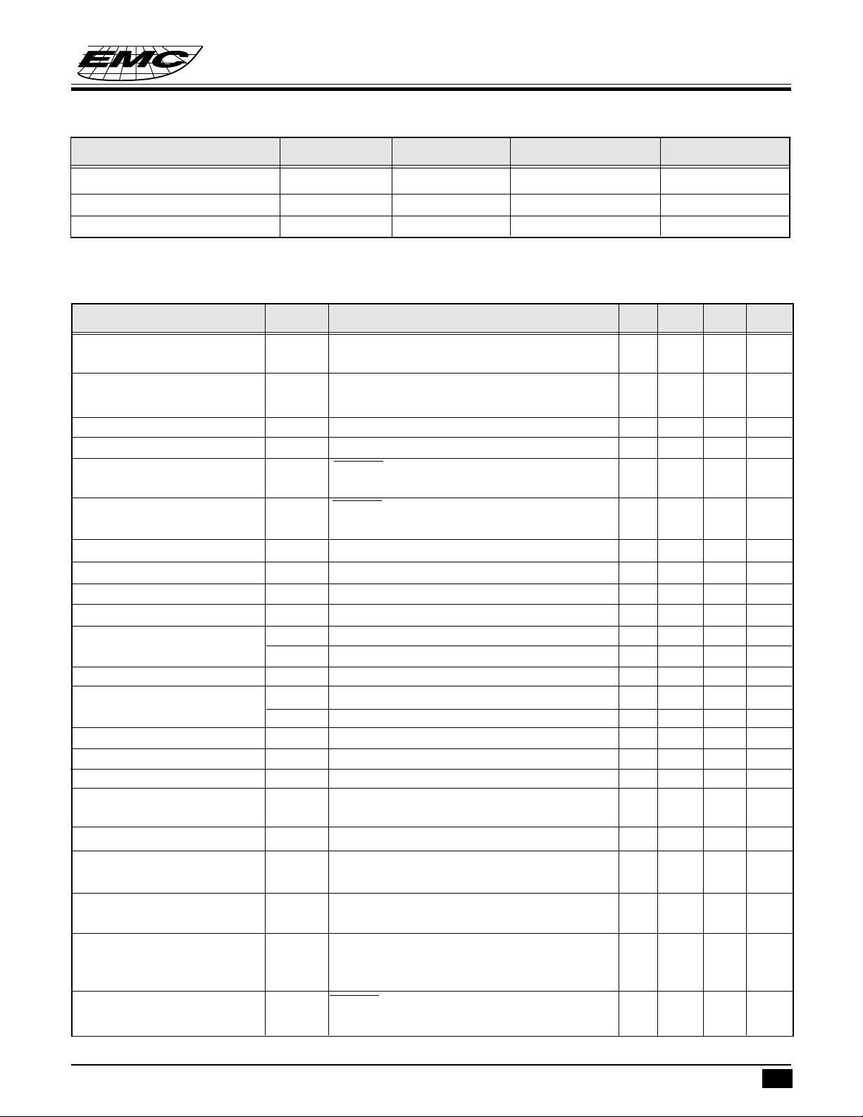
ABSOLUTE MAXIMUM RATINGS
Items Sym. Condition Rating Unit
EM78860
Temperature under bias V
Input voltage V
Operating temperature range T
DD
IN
A
-0.3 to 6 V
- 0.5 to VDD+ 0.5 V
0 to 70 °C
DC ELECTRICAL CHARACTERISTICS
(T
= 0°C~70°C, V
A
Parameter Sym. Condition Min. Typ. Max. Unit
Input Leakage Current I
for input pins
Input Leakage Current I
for bi-directional pins
Input High Voltage V
Input Low voltage V
Input High Threshold V
Voltage
Input Low Threshold V
Voltage
Clock Input High Voltage V
Clock Input Low Voltage V
Key scan Input High Voltage VHscan Port6 for key scan 3.5 V
Key scan Input Low Voltage VLscan Port6 for key scan 1.5 V
Output High Voltage V
(port5,6,7,8)
(port9) I
Output Low Voltage V
(port5,6,7,8)
(port9) I
Com Voltage drop V
Segment Voltage drop V
LCD Drive Reference V
Voltage
Pull-high Current I
Power Down Current I
IDLE mode current I
Low Clock Current I
Operating Supply Current I
= 5V±5%; VSS = 0V)
DD
IL1
IL2
IH
IL
IHT
ILT
IHX
ILX
OH1
OL1
COM
SEG
LCD
PH
SB1
SB-1
SB2
CC
V
= VDD, V
IN
VIN = V
DD
, V
SS
SS
±1 µA
± 1 µA
2.5 V
0.8 V
RESET, TCC, RDET1 2.0 V
RESET, TCC, RDET1 0.8 V
OSCI 3.5 V
OSCI 1.5 V
I
= ±1.6 mA 2.4 V
OH
= ±6 mA 2.4 V
OH
IOL = ±1.6 mA 0.4 V
= ±6 mA 0.4 V
OL
I O = ±50 µA - - 2.9 V
I O = ±50 µA - - 3.8 V
Contrast adjustment
Pull-high active input pin at V
SS
-50 -100 -240 µA
All input and I/O pin at VDD,3µA
output pin floating, WDT disabled
All input and I/O pin at VDD, output pin 80 µA
floating, WDT disabled,LCD enable
CLK=32.768 KHz, All input and I/O pin 90 µA
at V
, output pin floating, WDT disabled,
DD
LCD enable
RESET=HIGH, CLK=3.679MHz, output pin 1.5 mA
floating
* This specification are subject to be changed without notice.
6.24.1998
22
Page 23
EM78860
8-BIT MICRO-CONTROLLER
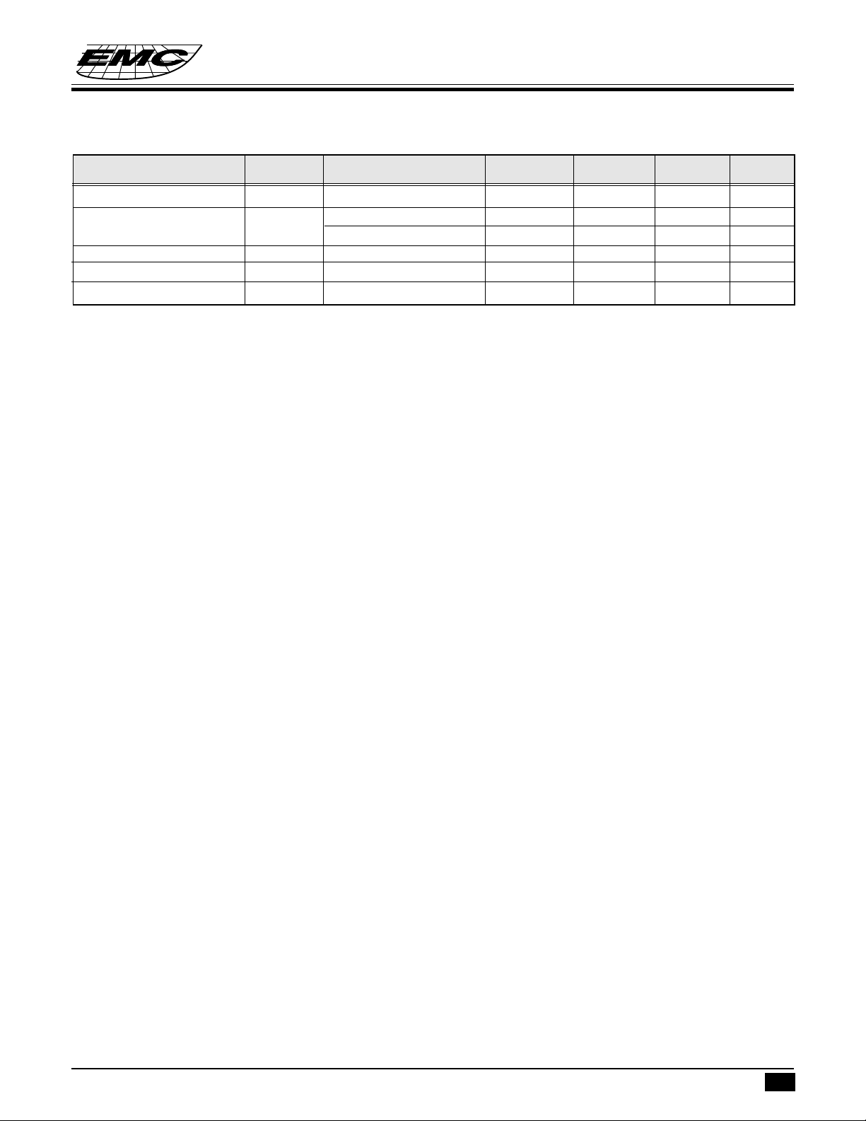
AC ELECTRICAL CHARACTERISTIC ( T
= 0 ~ 70°C, V
A
= 5V,VSS = 0V )
DD
Parameter Sym. Condition Min. Typ. Max. Unit
Input CLK duty cycle Dclk 45 50 55 %
Instruction cycle time Tins 32.768K 60 µs
3.679M 550 µs
Device delay hold time Tdrh 18 ms
TCC input period Ttcc Note 1 (Tin+20)/N ns
Watchdog timer period Twdt T
= 25°C18ms
A
Note 1: N = selected prescaler ratio.
* This specification are subject to be changed without notice.
6.24.1998
23
Page 24
TIMING DIAGRAMS
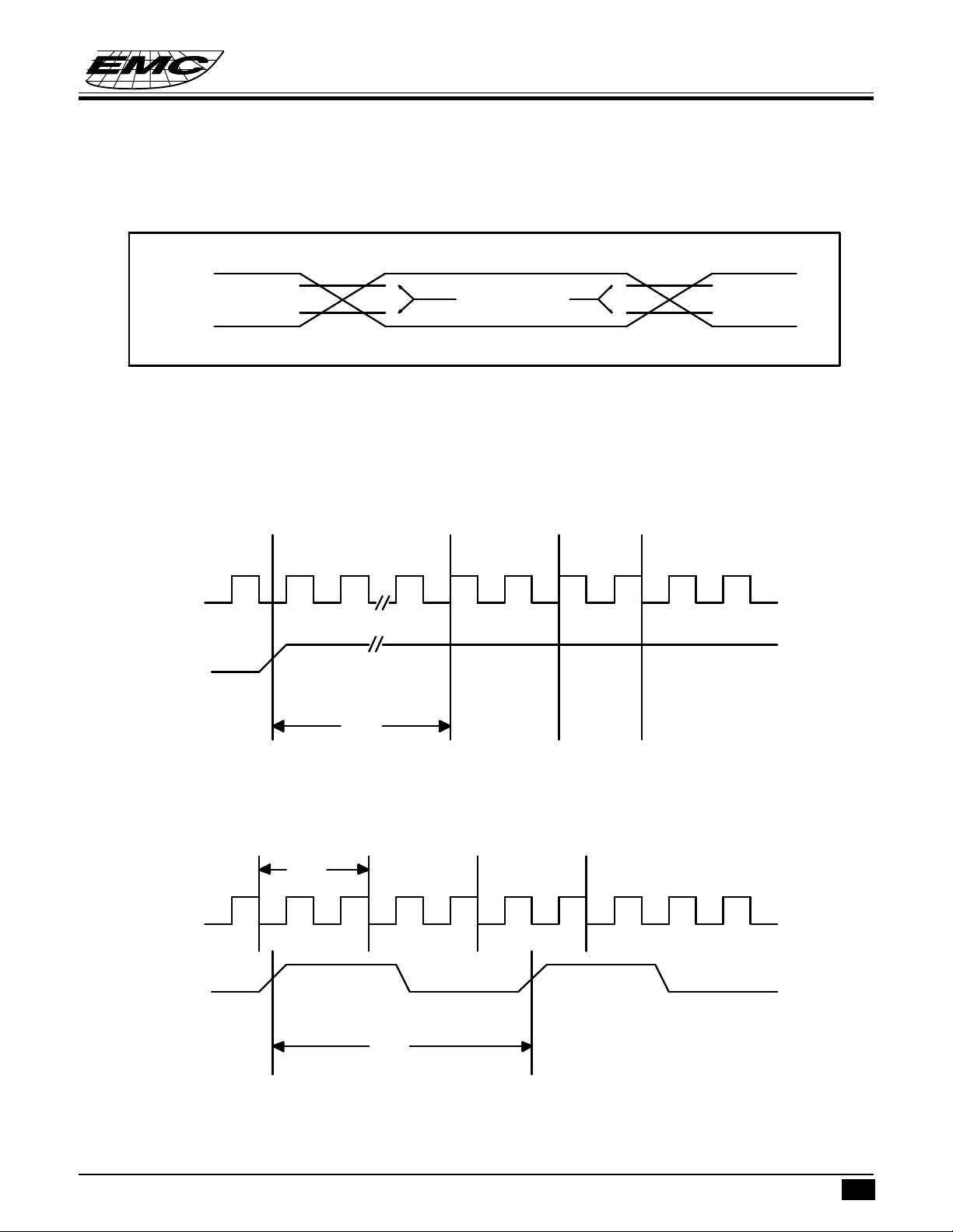
AC Test Input/Output Waveform
EM78860
8-BIT MICRO-CONTROLLER
2.4
2.0
0.8
0.45
2.0
0.8
AC Testing : Input are driven at 2.4V for logic "1", and 0.45V for logic "0". Timing
measurements are made at 2.0V for logic "1", and 0.8V for logic "0".
RESET Timing
NOP
Instruction 1
Executed
TCC Input Timing
CLK
TCC
Tdrh
Tins
Ttcc
Fig.17 AC timing
* This specification are subject to be changed without notice.
6.24.1998
24
Page 25
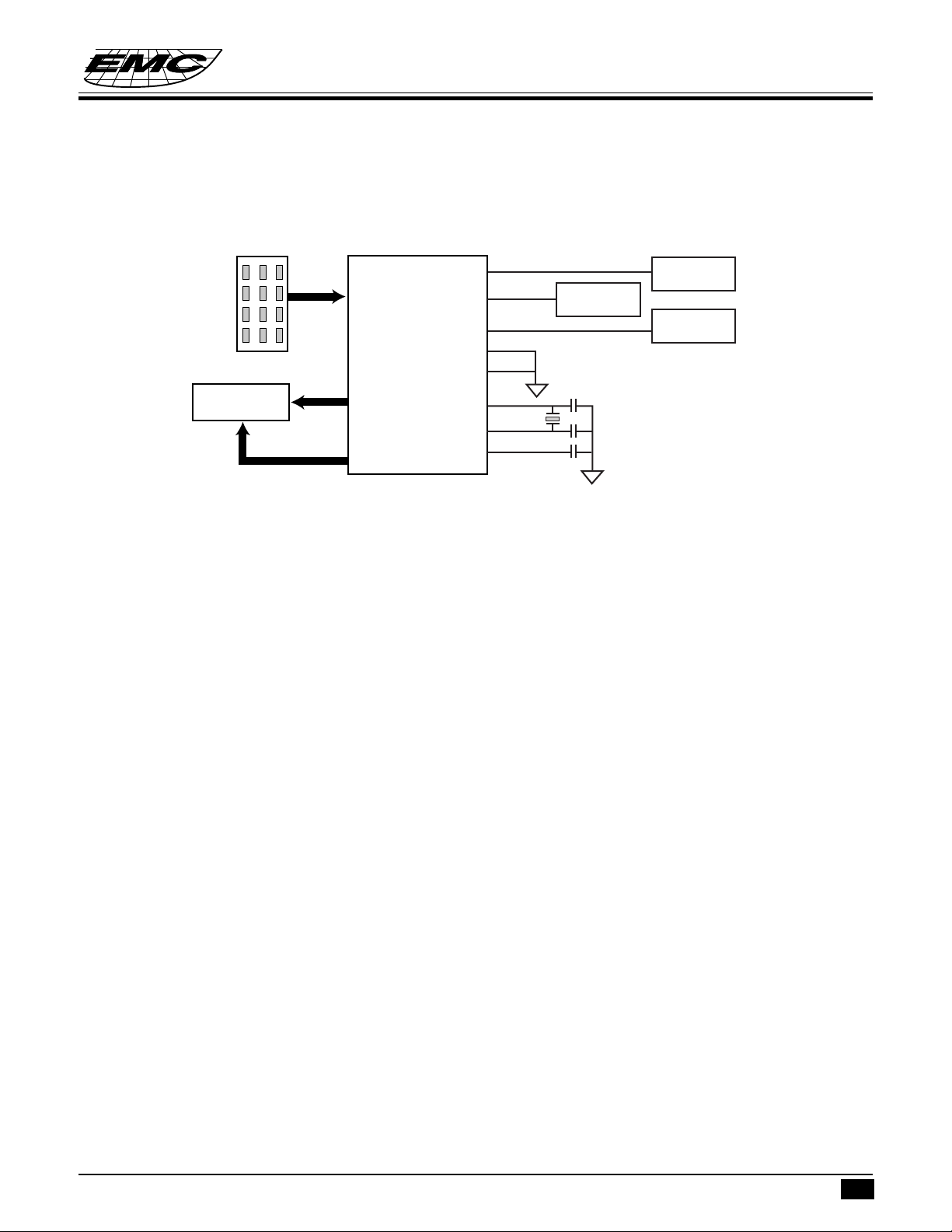
APPLICATION CIRCUIT
kEYPAD
EMC78860 LCD
I/O
EM78860
COMMON
SEGMENT
VDD
LOBAT
/RESET
TEST
GND
XIN
XOUT
PLLC
32768
BATTERY
DETECTOR
30p
30p
0.01µ
EM78860
8-BIT MICRO-CONTROLLER
CD POWER
SUPPLY
POWER ON
RESET
* This specification are subject to be changed without notice.
6.24.1998
25
 Loading...