

Page 1

EM78P156E
I. GENERAL DESCRIPTION
EM78P156E is an 8-bit microprocessor with low-power and high-speed CMOS technology. There is a 1K*13bit Electrical One Time Programmable Read Only Memory (OTP-ROM) within it. It provides a PROTECTION
bit to prevent a user’s code from intruding as well as 7 OPTION bits to match the user’s requirements.
Because of the OTP-ROM, the EM78P156E offers users a convenient way to develop and verify their programs.
Moreover, a user’s developed code can be programmed easily by an EMC writer.
II. FEATURES
• Operating voltage range: 2.2V~5.5V
• Available in temperature range: 0°C~70°C
• Operating frequency range: DC ~ 36MHz
• Low power consumption:
* less than 1.6 mA at 5V/4MHz
* typical of 15 µA at 3V/32KHz
* typical of 1 µA during the sleep mode
• 1Kx13 bits on chip ROM
• One security register to prevent the code in the OTP memory from intruding
• One configuration register to match the user’s requirements
• 48x8 bits on chip registers (SRAM)
• 2 bi-directional I/O ports
• 5 level stacks for subroutine nesting
• 8-bit real time clock/counter (TCC) with selective signal sources, trigger edges, and overflow interrupt
• Two clocks per instruction cycle
• Power-down mode (SLEEP mode)
• Three available interruptions
* TCC overflow interrupt
* Input-port status changed interrupt (wake up from the sleep mode)
* External interrupt
• Programmable free running watchdog timer
• 8 pull-high pins
• 7 pull-down pins
• 8 open-drain pins
• Two R-option pins
• Package type: SOP, SOIC and DIP
• 99.9% single instruction cycle commands
* This specification is subject to be changed without notice. 8.11.1999
B3-1
Page 2
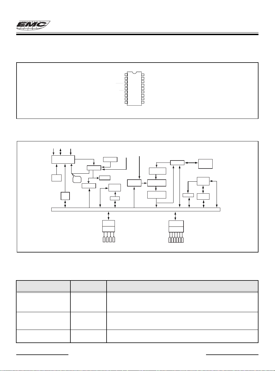
III. PIN ASSIGNMENTS
EM78P156E
EM78P156E
P52
1
P53
2
TCC
3
RESET
4
SS
V
5
P60,INT
6
P61
7
P62
8
P63
9
DIP
SOP
SOIC
Fig. 1 Pin assignments
IV. FUNCTIONAL BLOCK DIAGRAM
OSCI OSCO /RESET
Oscillator/Timing
Control
Internal C
External R
oscillator
Sleep
& Wake
Control
WDT
Time-out
WDT Timer
Prescaler
IOCA
R1(TCC)
IOC5
TCC
Interrupt
RAM
Controller
R4
DATA & CONTROL BUS
R5
/INT
P51
18
P50
17
OSCI
16
OSCO
15
V
DD
14
P67
13
P66
12
P65
11
P64
10
R2
Stack
ROM
Instruction
register
Instruction
Decoder
ALU
R3
ACC
IOC6
R6
P
P
P
P
5
5
5
5
0
2
3
1
P
P
P
P
P
P
P
P
6
6
6
6
6
6
6
6
0
2
3
1
4
6
7
5
Fig. 2 Functional block diagram
V. PIN DESCRIPTION
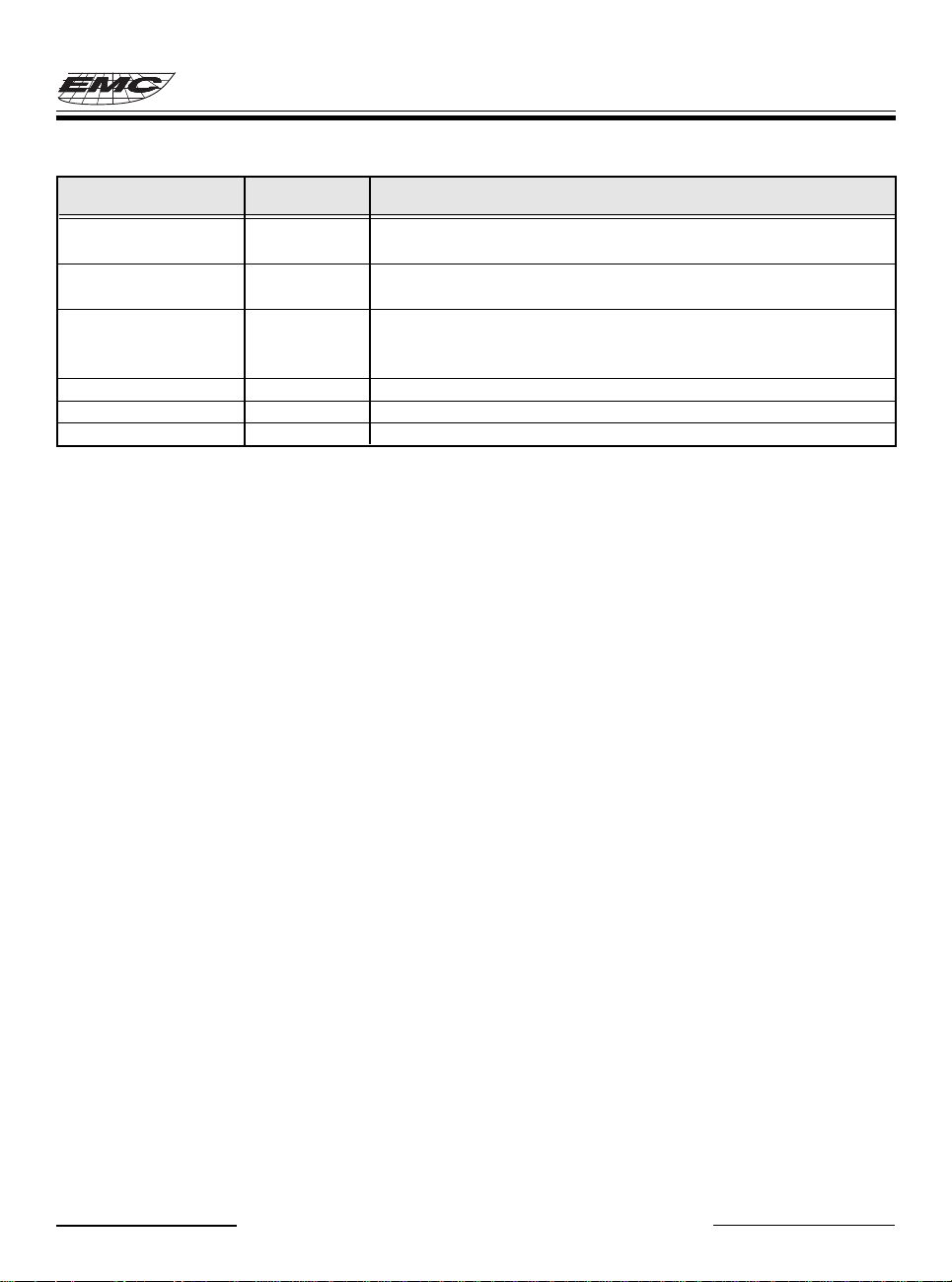
Table 1 Pin description-EM78P156E
Symbol I/O Function
OSCI I *XTAL type : Crystal input terminal or external clock input pin.
*ERC type: RC oscillator input pin.
*IRC type: 50K ohm pulled high for 4MHz.
OSCO I/O * XTAL type: Output terminal for crystal oscillator or external clock input pin.
*RC type: Instruction clock ouput.
*External clock signal input.
TCC I * Real time clock/counter with Schmitt trigger input pin, must be tied to V
or VSS if not in use.
* This specification is subject to be changed without notice. 8.11.1999
B3-2
DD
Page 3
EM78P156E
Symbol I/O Function
/RESET I * Input pin with Schmitt trigger. If this pin remains at logic low, the controller
will keep in reset condition.
P50~P53 I/O *P50~P53 are bi-directional I/O pins. P50 and P51 can also be defined as the
R-option pins. P50~P52 can be pulled down by software .
P60~P67 I/O *P60~P67 are bi-directional I/O pins. These can be pull-high or can be open-
drain by software programming. In addition, P60~P63 can be pull-down
also by software.
/INT I * External interrupt pin triggered by falling edge.
V
DD
V
SS
VI. FUNCTION DESCRIPTION
VI.1 Operational Registers
1. R0 (Indirect Addressing Register)
• R0 is not a physically implemented register. Its major function is to be an indirect addressing pointer. Any instruction
using R0 as a pointer actually accesses data pointed by the RAM Select Register (R4).
- * Power supply.
- * Ground.
2. R1 (Time Clock /Counter)
• Increased by an external signal edge which is defined by TE bit (CONT-4) through the TCC pin,
or by the instruction cycle clock.
• Writable and readable as any other registers.
3. R2 (Program Counter) & Stack
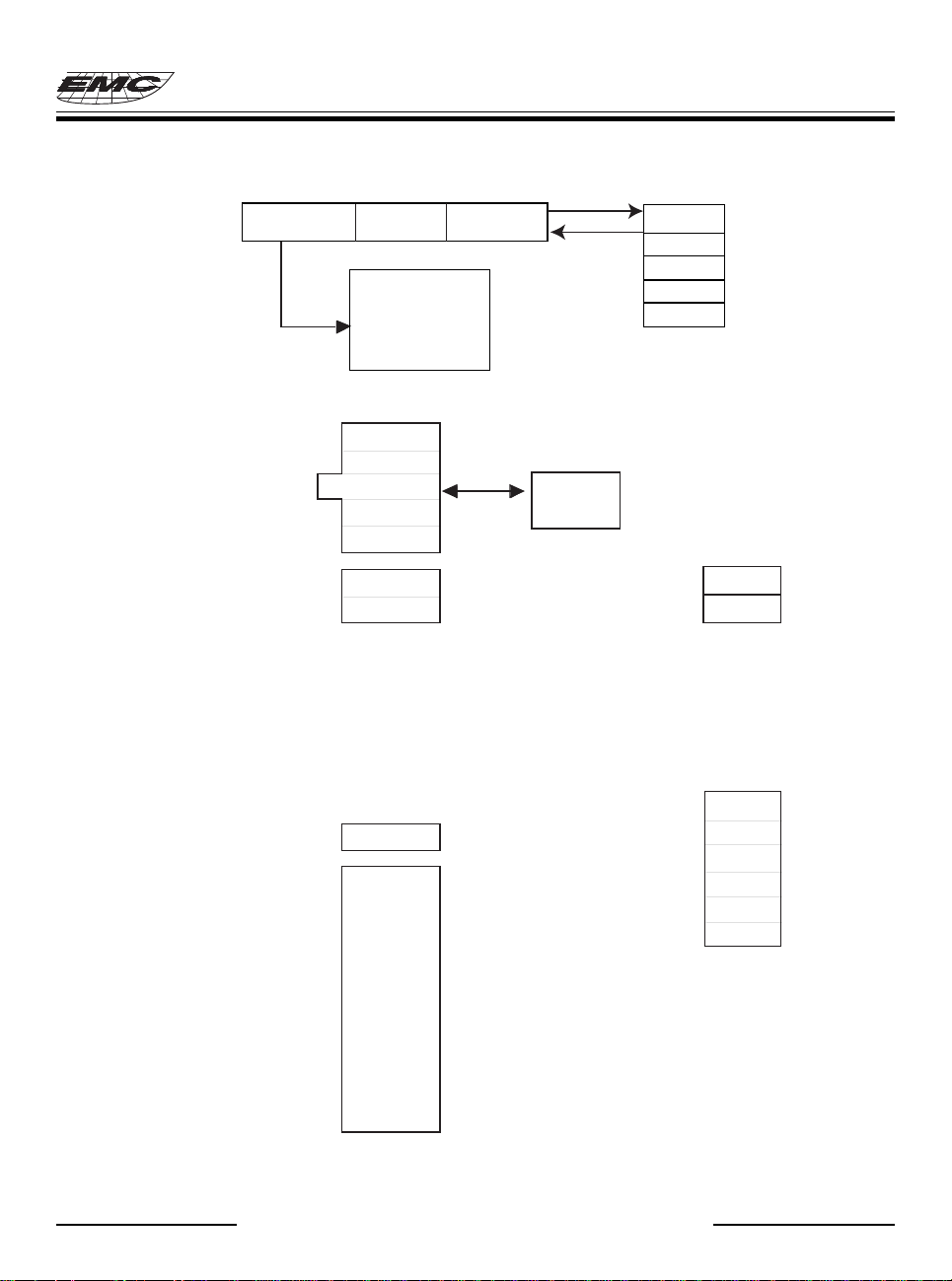
• R2 and hardware stacks are 10~12-bit wide. The structure is depicted in Fig. 3.
• Generating 1024x13 bits on-chip OTP ROM addresses to the relative programming instruction codes. One program
page is 1024 words long.
• The contents of R2 are set all “0”s upon a RESET condition.
• “JMP” instruction allows the direct loading of the lower 10 program counter bits. Thus, “JMP” allows PC to go to
any location within a page.
• “CALL” instruction loads the lower 10 bits of the PC, and then PC+1 is pushed into the stack. Thus, the subroutine
entry address can locate anywhere within a page.
“ RET” (“RETL K”, “RETI”) instruction loads the program counter with the contents of the top-level stack.
“ADD R2,A” allows a relative address to be added to the current PC, and the ninth and tenth bits of the PC are cleared.
• “MOV R2,A” allows to load an address from the “A” register to the lower 8 bits of the PC, and the ninth and tenth
bits of the PC are cleared.
• Any instruction which would change the contents of R2 (e.g. “ADD R2,A”, “MOV R2,A”, “BC R2,6”,......) will
cause the ninth and tenth bits (A8~A9) of the PC to be cleared. Thus, the computed jump is limited to the first
256 locations of a page.
• All instructions are single instruction cycle (fclk/2) except the instructions which would change the contents of R2
need one more instruction cycle.
* This specification is subject to be changed without notice. 8.11.1999
B3-3
Page 4
CALL
IOC5
IOC6
IOCA
IOCB
IOCC
IOCD
IOCE
IOCF
Stack
(5 levels)
R0
R1(TCC)
R2(PC)
R3(Status)
R4(RSR)
00
01
02
03
04
R5(Port5)
R6(Port6)
RF
R10
:
:
48x8
Common
Register
R3F
05
06
07
08
09
0A
0B
0C
0D
0E
0F
10
:
:
3F
A11 A10 A9 A8 A7 ~ A0 Stack 1
PC
RET
000
00
PAGE 0
3FF
Fig. 3 Program counter organization
RETI
RETL
EM78P156E
Stack 2
Stack 3
Stack 4
Stack 5
Fig. 4 Data memory configuration
* This specification is subject to be changed without notice. 8.11.1999
B3-4
Page 5
EM78P156E
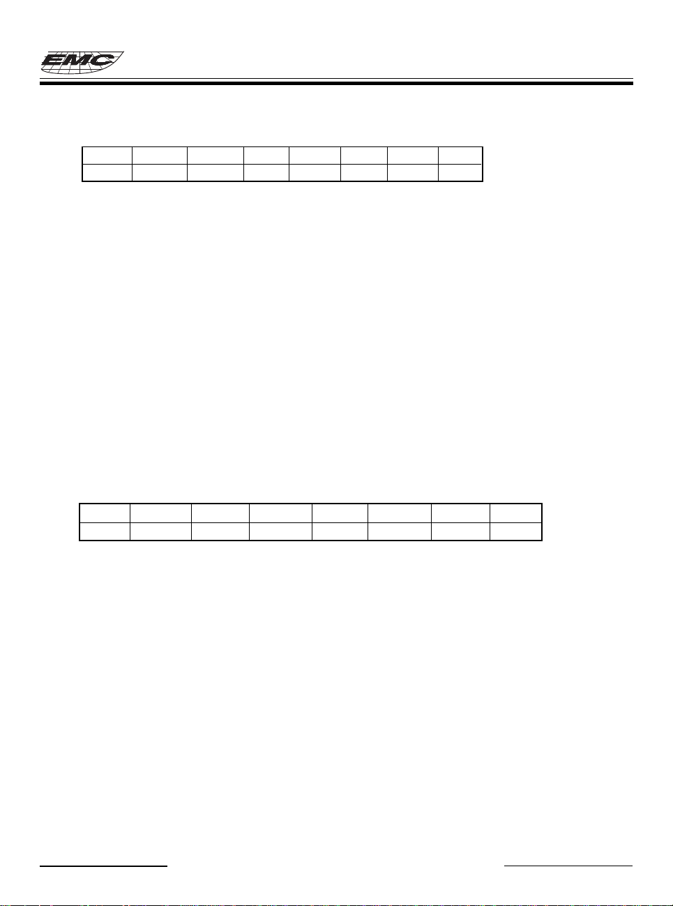
4. R3 (Status Register)
7 6 543210
GP2 GP1 GP0 T P Z DC C
• Bit 0 (C) Carry flag
• Bit 1 (DC) Auxiliary carry flag
• Bit 2 (Z) Zero flag. Set to "1" if the result of an arithmetic or logic operation is zero.
• Bit 3 (P) Power-down bit. Set to 1 during power-on or by a “WDTC” command and reset to 0 by a
“SLEP” command.
• Bit 4 (T) Time-out bit. Set to 1 by the “SLEP” and “WDTC” commands, or during power-up and reset
to 0 by WDT time-out.
• Bit 5~7 (GP0~2) General-purpose read/write bits.
5. R4 (RAM Select Register)
• Bits 0 ~ 5 are used to select registers (address: 00~06, 0F~3F) in the indirect addressing mode.
• Bits 6 ~ 7 are general-purpose read/write bits.
• See the configuration of the data memory in Fig.4.
6. R5 ~ R6 (Port 5 ~ Port 6)
• R5 and R6 are I/O registers.
• Only the lower 4 bits of R5 are available.
7. RF (Interrupt Status Register)
76 5 4 32 10
- - - - - EXIF ICIF TCIF
• "1" means interrupt request, and "0" means non-interrupt occurence.
• Bit 0 (TCIF) TCC overflowing interrupt flag. Set when TCC timer overflows, reset by software.
• Bit 1 (ICIF) Port 6 input status changed interrupt flag. Set when Port 6 input changes, reset by software.
• Bit 2 (EXIF) External interrupt flag. Set by falling edge on /INT pin, reset by software.
• Bits 3 ~ 7 Not used.
• RF can be cleared by instruction but can not be set.
• IOCF is the interrupt mask register.
• Note that the result of reading RF is the "logic AND" of RF and IOCF.
8. R10 ~ R3F
• All of these are the 8-bit general-purpose registers.
VI.2 Special Purpose Registers
1. A (Accumulator)
* This specification is subject to be changed without notice. 8.11.1999
B3-5
Page 6
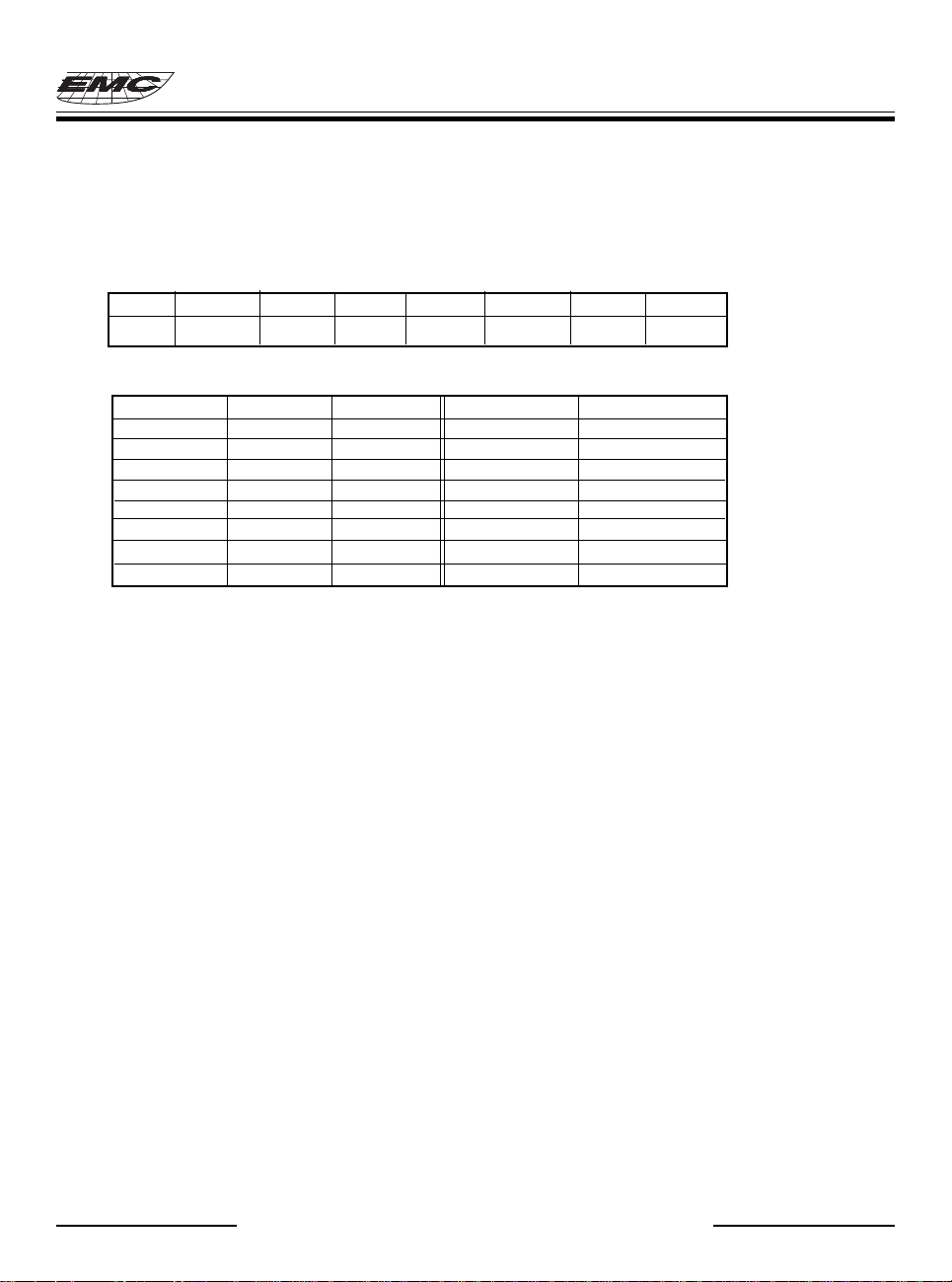
• Internal data transfer, or instruction operand holding
• It can not be addressed.
2. CONT (Control Register)
76 543 21 0
- /INT TS TE PAB PSR2 PSR1 PSR0
Bit 0 (PSR0)~Bit 2 (PSR2) TCC/WDT prescaler bits.
PSR2 PSR1 PSR0 TCC Rate WDT Rate
0 0 0 1:2 1:1
0 0 1 1:4 1:2
0 1 0 1:8 1:4
0 1 1 1:16 1:8
1 0 0 1:32 1:16
1 0 1 1:64 1:32
1 1 0 1:128 1:64
1 1 1 1:256 1:128
Bit 3 (PAB) Prescaler assignment bit.
0: TCC
1: WDT
Bit 4 (TE) TCC signal edge
0: increment if the transition from high to low takes place on TCC pin
1: increment if the transition from high to low takes place on TCC pin
Bit 5 (TS) TCC signal source
0: internal instruction cycle clock
1: transition on TCC pin
Bit 6 (INT) Interrupt enable flag
0: masked by DISI or hardware interrupt
1: enabled by ENI/RETI instruction
• CONT register is both readable and writable.
EM78P156E
3. IOC5 ~ IOC6 (I/O Port Control Register)
• “1” puts the relative I/O pin into high impedance, while “0” defines the relative I/O pin as output.
• Only the lower 4 bits of IOC5 are able to be defined.
• IOC5 and IOC6 registers are both readable and writable.
4. IOCA (Prescaler Counter Register)
• IOCA register is readable.
• The value of IOCA is equal to the contents of Prescaler counter.
• Down counter.
* This specification is subject to be changed without notice. 8.11.1999
B3-6
Page 7
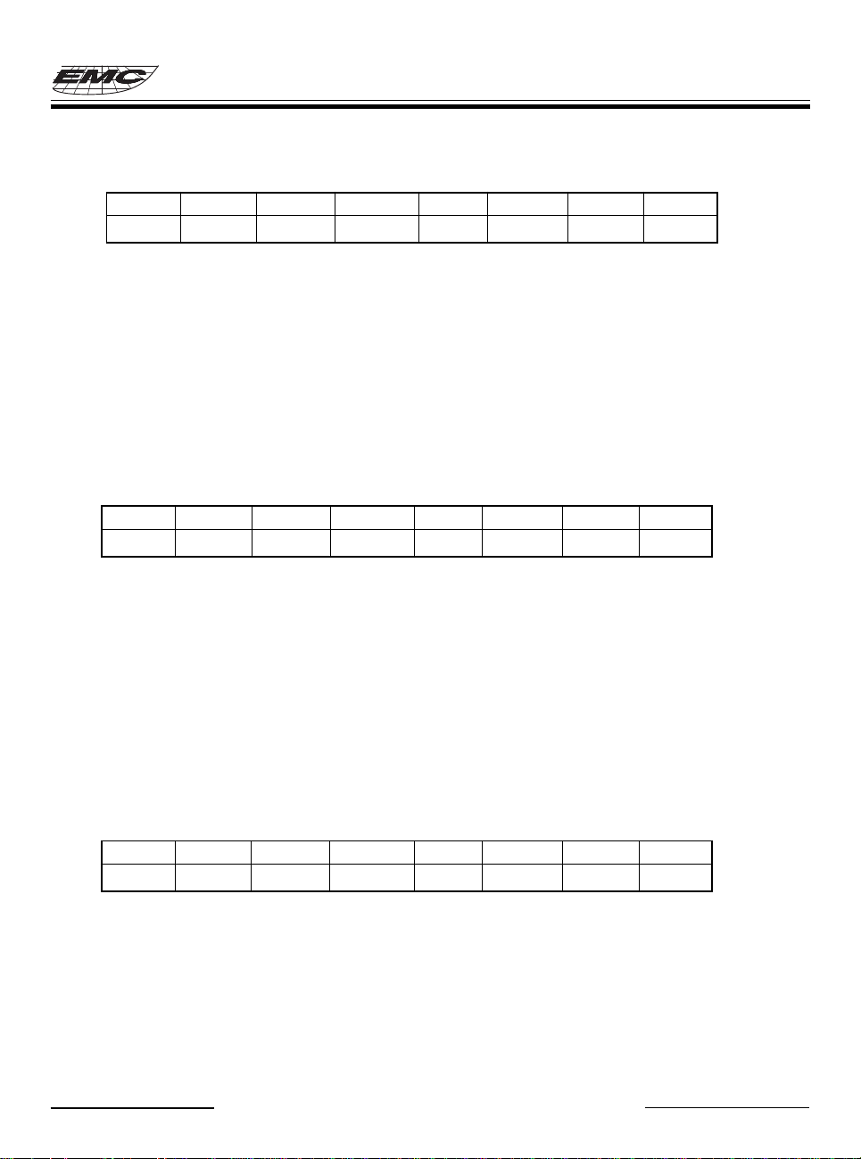
5. IOCB (Pull-down Control Register)
76543210
/PD7 /PD6 /PD5 /PD4 - /PD2 /PD1 /PD0
Bit 0 (/PD0) Control bit used to enable the pull-down of P50 pin.
0: Enable internal pull-down
1: Disable internal pull-down
Bit 1 (/PD1) Control bit used to enable the pull-down of P51 pin.
Bit 2 (/PD2) Control bit used to enable the pull-down of P52 pin.
Bit 3 Not used.
Bit 4 (/PD4) Control bit used to enable the pull-down of P60 pin.
Bit 5 (/PD5) Control bit used to enable the pull-down of P61 pin.
Bit 6 (/PD6) Control bit used to enable the pull-down of P62 pin.
Bit 7 (/PD7) Control bit used to enable the pull-down of P63 pin.
• IOCB register is both readable and writable.
6. IOCC (Open-drain Control Register)
76543210
OD7 OD6 OD5 OD4 OD3 OD2 OD1 OD0
Bit 0 (OD0) Control bit used to enable the open-drain of P60 pin.
0: Disable open-drain output
1: Enable open-drain output
Bit 1 (OD1) Control bit used to enable the open-drain of P61 pin.
Bit 2 (OD2) Control bit used to enable the open-drain of P62 pin.
Bit 3 (OD3) Control bit used to enable the open-drain of P63 pin.
Bit 4 (OD4) Control bit used to enable the open-drain of P64 pin.
Bit 5 (OD5) Control bit used to enable the open-drain of P65 pin.
Bit 6 (OD6) Control bit used to enable the open-drain of P66 pin.
Bit 7 (OD7) Control bit used to enable the open-drain of P67 pin.
• IOCC register is both readable and writable.
EM78P156E
7. IOCD (Pull-high Control Register)
765 43210
/PH7 /PH6 /PH5 /PH4 /PH3 /PH2 /PH1 /PH0
Bit 0 (/PH0) Control bit used to enable the pull-high of P60 pin.
0: Enable internal pull-high
1: Disable internal pull-high
Bit 1 (/PH1) Control bit used to enable the pull-high of P61 pin.
Bit 2 (/PH2) Control bit used to enable the pull-high of P62 pin.
Bit 3 (/PH3) Control bit used to enable the pull-high of P63 pin.
Bit 4 (/PH4) Control bit used to enable the pull-high of P64 pin.
Bit 5 (/PH5) Control bit used to enable the pull-high of P65 pin.
* This specification is subject to be changed without notice. 8.11.1999
B3-7
Page 8
EM78P156E
Bit 6 (/PH6) Control bit used to enable the pull-high of P66 pin.
Bit 7 (/PH7) Control bit used to enable the pull-high of P67 pin.
• IOCD register is readable and writable.
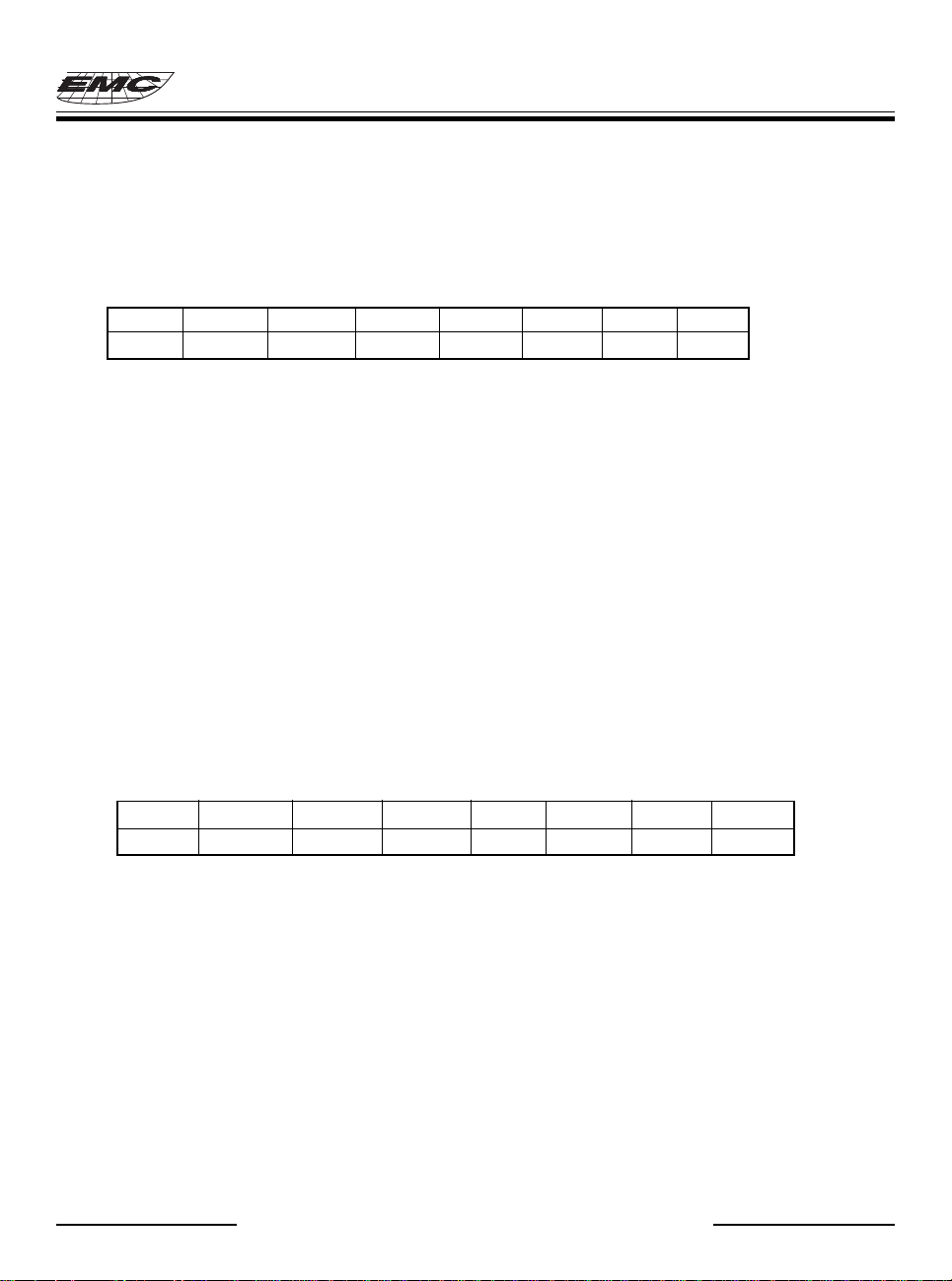
8. IOCE (WDT Control Register)
76543210
WDTE EIS - ROC - - - -
Bit 7 (WDTE) Control bit used to enable Watchdog Timer.
0: Disable WDT.
1: Enable WDT.
• WDTE is both readable and writable.
Bit 6 (EIS) Control bit used to define the function of P60 (/INT) pin.
0: P60, bi-directional I/O pin.
1: /INT, external interrupt pin. In this case, the I/O control bit of P60 (bit 0 of IOC6) must be set to “1”.
• When EIS is “0”, the path of /INT is masked. When EIS is “1”, the status of /INT pin can also be read by
way of reading Port 6 (R6). Refer to Fig.7(a).
• EIS is both readable and writable.
Bit 4 (ROC) ROC is used for the R-option.
Setting the ROC to “1” will enable the status of R-option pins (P50~P51) to be read by the controller. Clearing
the ROC will disable the R-option function. If the R-option function is selected, the user must connect the P51
pin or/and P50 pin to VSS by a 430KΩ external resistor (Rex). If the Rex is connected/disconnected, the status
of P50 (P51) will be read as “0”/”1". Refer to Fig.8.
• ROC is readable and writable.
Bits 0~3, 5 Not used.
9. IOCF (Interrupt Mask Register)
76543210
- - - - - EXIE ICIE TCIE
Bit 0 (TCIE) TCIF interrupt enable bit.
0: disable TCIF interrupt
1: enable TCIF interrupt
Bit 1 (ICIE) ICIF interrupt enable bit.
0: disable ICIF interrupt
1: enable ICIF interrupt
Bit 2 (EXIE) EXIF interrupt enable bit.
0: disable EXIF interrupt
1: enable EXIF interrupt
Bits 3~7 Not used.
• Individual interrupt is enabled by setting its associated control bit in the IOCF to “1”.
• Global interrupt is enabled by the ENI instruction and is disabled by the DISI instruction. Refer to Fig.10.
• IOCF register is both readable and writable.
* This specification is subject to be changed without notice. 8.11.1999
B3-8
Page 9
EM78P156E
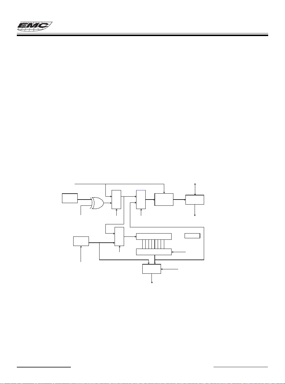
VI.3 TCC/WDT & Prescaler
There is an 8-bit counter available as prescaler for the TCC or WDT. The prescaler is available for the TCC only
or the WDT only at the same time and the PAB bit of the CONT register is used to determine the prescaler assigment.
The PSR0~PSR2 bits determine the ratio. The prescaler will be cleared by the instructions which write to TCC each time,
when assigned to TCC mode. The WDT and prescaler, when assigned to WDT mode, will be cleared by the “WDTC”
and “SLEP” instructions. Fig.5 depicts the circuit diagram of TCC/WDT.
• R1 (TCC) is an 8-bit timer/counter. The clock source of TCC can be internal clock or external clock input (edge
selectable from TCC pin). If TCC signal source is from internal clock, TCC will increase by 1 in every instruction
cycle (without prescaler). Refer to Fig.5, CLK=Fosc/2 or CLK=Fosc/4 is depended on the CODE option bit CLKS.
CLK=Fosc/2 if CLKS bit is “0”, and CLK=Fosc/4 if CLKS bit is “1”. If TCC signal source is from external clock
input, TCC will increase by 1 on every falling edge or rising edge of TCC pin.
• The watchdog timer is a free running on-chip RC oscillator. The WDT will keep running even the oscillator driver
has been turned off (i.e. in sleep mode). During the normal operation or the sleep mode, a WDT time-out (if enabled)
will cause the device to reset. The WDT can be enabled or disabled at any time during the normal mode by software
programming. Refer to WDTE bit of IOCE register. With no presacler, the WDT time-out period is approximately
18 ms.
CLK(Fosc/2 or Fosc/4)
TCC
Pin
Data Bus
0
1
1
M
U
X
M
U
X
0
SYNC
2 cycles
TCC(R1)
TE
WDT
WDTE
(in IOCE)
TS PAB
0
M
U
1
X
PAB
8-bit Counter
8-to-1 MUX
1
0
MUX
WDT time-out
TCC overflow interrupt
IOCA
PSR0 ~PSR2
PAB
Fig. 5 Block diagram of TCC and WDT
VI.4 I/O Ports
The I/O registers, both Port 5 and Port 6, are bi-directional tri-state I/O ports. Port 6 can be pulled high internally
by software. In addition, Port 6 can also have open-drain output by software. There is an input status changed interrupt
(or wake-up) function on Port 6. P50 ~ P52 and P60 ~ P63 pins can be pulled down by software. Each I/O pin can be
defined as “input” or “output” pin by the I/O control registers (IOC5 ~ IOC6). P50~P51 are the R-option pins enabled
by setting the ROC bit in the IOCE register to 1. While the R-option function is used, P50~P51 are recommended to be
used as output pins. During the period of R-option being enabled, P50~P51 must be programmed as input pins. In the
R-option mode, the current consuming by the Rex should be taken into the consideration, if the low power consumption
is concerned.
* This specification is subject to be changed without notice. 8.11.1999
B3-9
Page 10
EM78P156E
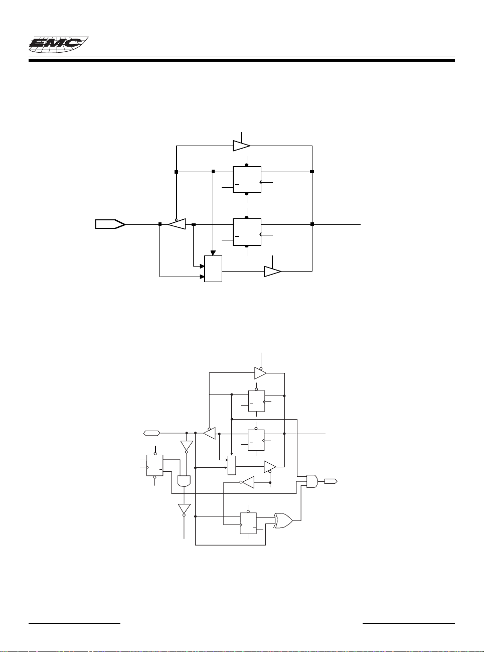
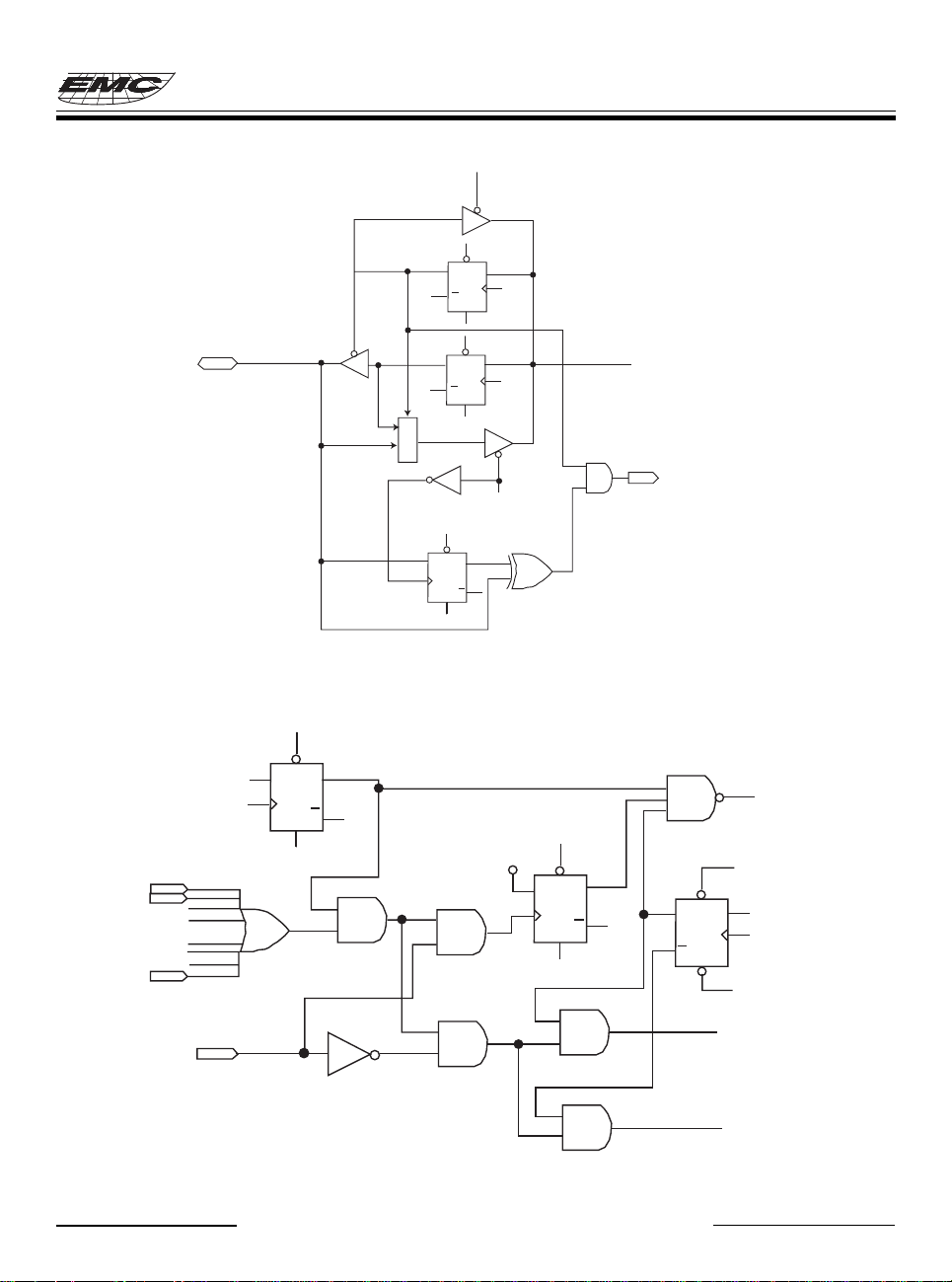
The I/O registers and I/O control registers are both readable and writable. The I/O interface circuits for Port 5 and
Port 6 are shown in Fig.6 and Fig.7(a), 7(b) respectively.
PCRD
P
DQ
R
CLK
PCWR
P
CLK
DQ
PDWR
IOD
PDRD
PORT
C
Q
L
R
C
Q
L
0
M
U
1
X
*Pull-down is not shown in the figure.
Fig. 6 The circuit of I/O port and I/O control register for Port 5
PCRD
P
Q
D
R
CLK
PCWR
Q
C
L
P60, /INT
PORT
D
CLK
P
Q
R
C
Q
L
Bit 6 of IOCE
P
Q
D
R
CLK
PDWR
Q
C
0
1
INT
L
M
U
X
PDRD
P
D
Q
R
CLK
C
Q
L
IOD
TI0
*Pull-high (down) and open-drain are not shown in the figure.
Fig. 7(a) The circuit of I/O port and I/O control register for P60(/INT)
* This specification is subject to be changed without notice. 8.11.1999
B3-10
Page 11
EM78P156E
PCRD
P
Q
D
R
CLK
PCWR
Q
C
L
P61~P67
PORT
P
Q
D
R
CLK
PDWR
Q
C
L
0
M
1
U
X
PDRD
P
D
Q
R
CLK
C
Q
L
IOD
TIn
*Pull-high (down) and open-drain are not shown in the figure.
Fig. 7(b) The circuit of I/O port and I/O control register for P61~P67
IOCF.1
P
D
Q
R
CLK
C
Q
L
D
CLK
RF.1
P
Q
R
C
Q
L
P
Q
R
CLK
C
Q
L
VCC
TI0
TI1
TI7
Interrupt
ENI instruction
D
DISI instruction
/SLEP
Fig. 7(c) Block diagram of I/O Port 6 with input changed interrupt/wake-up
* This specification is subject to be changed without notice. 8.11.1999
B3-11
Interrupt
(Wake-up from SLEEP)
Next Instruction
(Wake-up from SLEEP)
Page 12
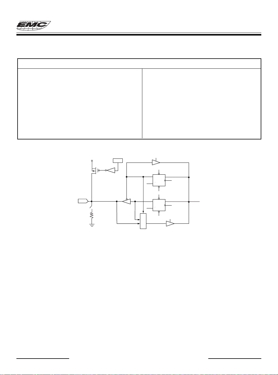
Table 2 Usage of Port 6 input changed wake-up/interrupt function
Usage of Port 6 Input Status Changed Wake-up/Interrupt
(I) Wake-up from Port 6 input status changed (II) Port 6 input status changed Interrupt
(a) Before SLEEP 1. Read I/O Port 6 (MOV R6,R6)
1. Disable WDT
1
(using very carefully) 2. Execute "ENI"
2. Read I/O Port 6 (MOV R6,R6) 3. Enable interrupt (Set IOCF.1)
3. Execute "ENI" or "DISI" 4. If Port 6 changed (interrupt)
4. Enable interrupt (Set IOCF.1) → Interrupt vector (008H)
5. Execute “SLEP” instruction
(b) After wake-up
1. If "ENI" → Interrupt vector (008H)
2. If "DISI" → Next instruction
1
Note : Software disables WDT (watchdog timer) but hardware must be enabled before using port6 changed
wake-up function. (CODE Option Register, bit 11 (ENWDTB-) set to "1").
Weekly
Pull-up
VCC
ROC
EM78P156E
PCRD
P
Q
D
R
PCWR
CLK
C
Q
L
PORT
Rex *
0
1
* The Rex is 430K ohm external resistor.
P
Q
D
R
PDWR
CLK
C
Q
L
M
U
X
PDRD
IOD
Fig. 8 The circuit of I/O port with R-option (P50,P51)
VI.5 RESET and Wake-up
1. RESET
The RESET can be caused by
(1) Power-on reset
(2) /RESET pin input "low", or
(3) WDT time-out (if enabled).
Note that only power-on reset, or only voltage detector in Case (1) is enabled in the system by CODE option bit.
Refer to Fig. 9. The device will be kept in a RESET condition for a period of approx. 18ms (one-oscillator startup timer period) after the reset is detected. Once the RESET occurs, the following functions
are performed.
• The oscillator is running, or will be started.
• The Program Counter (R2) is set to all "0".
• All I/O port pins are configured as input mode (high-impedance state).
* This specification is subject to be changed without notice. 8.11.1999
B3-12
Page 13

EM78P156E
• The Watchdog Timer and prescaler are cleared.
• Upon power-on, the upper 3 bits of R3 are cleared.
• The bits of the CONT register are set to all “1” except the bit 6 (INT flag).
• The bits of the IOCA register are set to all “1”.
• The bits of the IOCB register are set to all “1”.
• The IOCC register is cleared.
• The bits of the IOCD register are set to all “1”.
• Bit 7 of the IOCE register is set to “1”, and Bits 4 and 6 are cleared.
• Bits 0~2 of RF register and bits 0~2 of IOCF register are cleared.
Executing the “SLEP” instruction can perform the sleep mode (power-down mode). While entering sleep
mode, WDT (if enabled) is cleared but keeps running. The controller can be awakened by
(1) external reset input on /RESET pin,
(2) WDT time-out (if enabled), or
(3) Port 6 input status changed (if enabled).
The first two cases will cause the EM78P156E to reset. The T and P flags of R3 can be used to determine the source
of the reset (wake-up). The last case is considered the continuation of program execution and the global interrupt
(“ENI” or “DISI” being executed) decides whether or not the controller branches to the interrupt vector following
wake-up. If ENI is executed before SLEP, the instruction will begin to execute from the address 008H after wakeup. If DISI is executed before SLEP, the instruction will restart from the place where is right next to SLEP after
wake-up.
Only one of the cases 2 and 3 can be enabled before entering the sleep mode. That is,
[a] if Port 6 input status changed interrupt is enabled before SLEP , WDT must be disabled by software; however,
the WDT bit in the option register is still enabled. Hence, the EM78P156E can be awakened only by case 1 or 3.
[b] if WDT is enabled before SLEP, Port 6 input status changed interrupt must be disabled. Hence, the EM78P156E
can be awakened only by case 1 or 2. Refer to the section on interrupt.
If Port 6 input status changed interrupt is used to wake up the EM78P156E (the case [a]), the following
instructions must be executed before SLEP:
MOV A, 0bxx000110 ; Select internal TCC clock
CONTW
CLR R1 ; Clear TCC and prescaler
MOV A, 0bxxxx1110 ; Select WDT prescaler
CONTW
WDTC ; Clear WDT and prescaler
MOV A, 0b0xxxxxxx ; Disable WDT
IOW RE
MOV R6, R6 ; Read Port 6
MOV A, 0b00000x1x ; Enable Port 6 input changed interrupt
IOW RF
ENI (or DISI) ; Enable (or disable) global interrupt
SLEP ; Sleep
NOP
One problem should be aware that after waking up from the sleep mode, WDT would enable automatically.
The WDT operation (being enabled or disabled) should be handled appropriately by software after waking up from
the sleep mode.
* This specification is subject to be changed without notice. 8.11.1999
B3-13
Page 14
EM78P156E
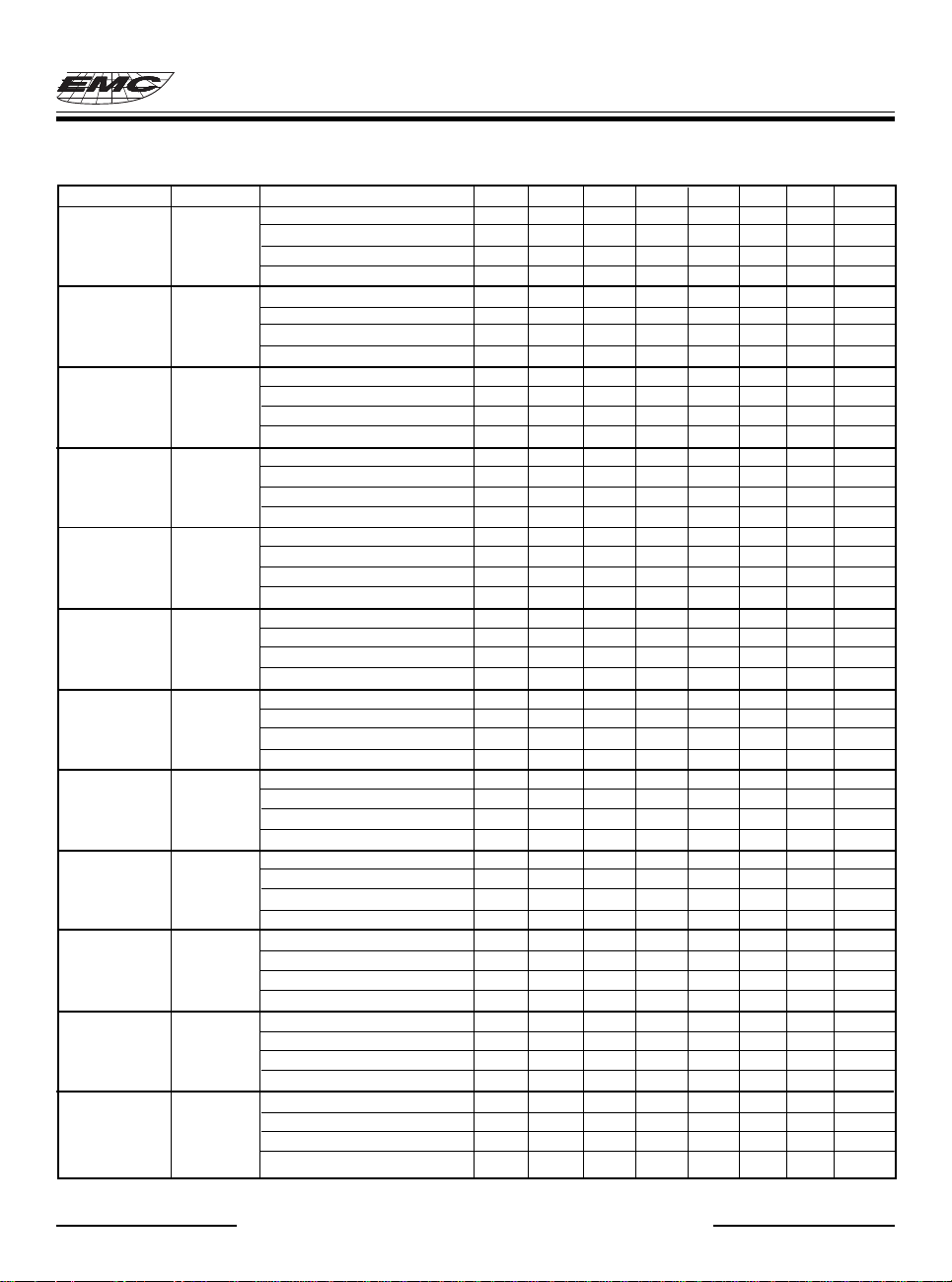
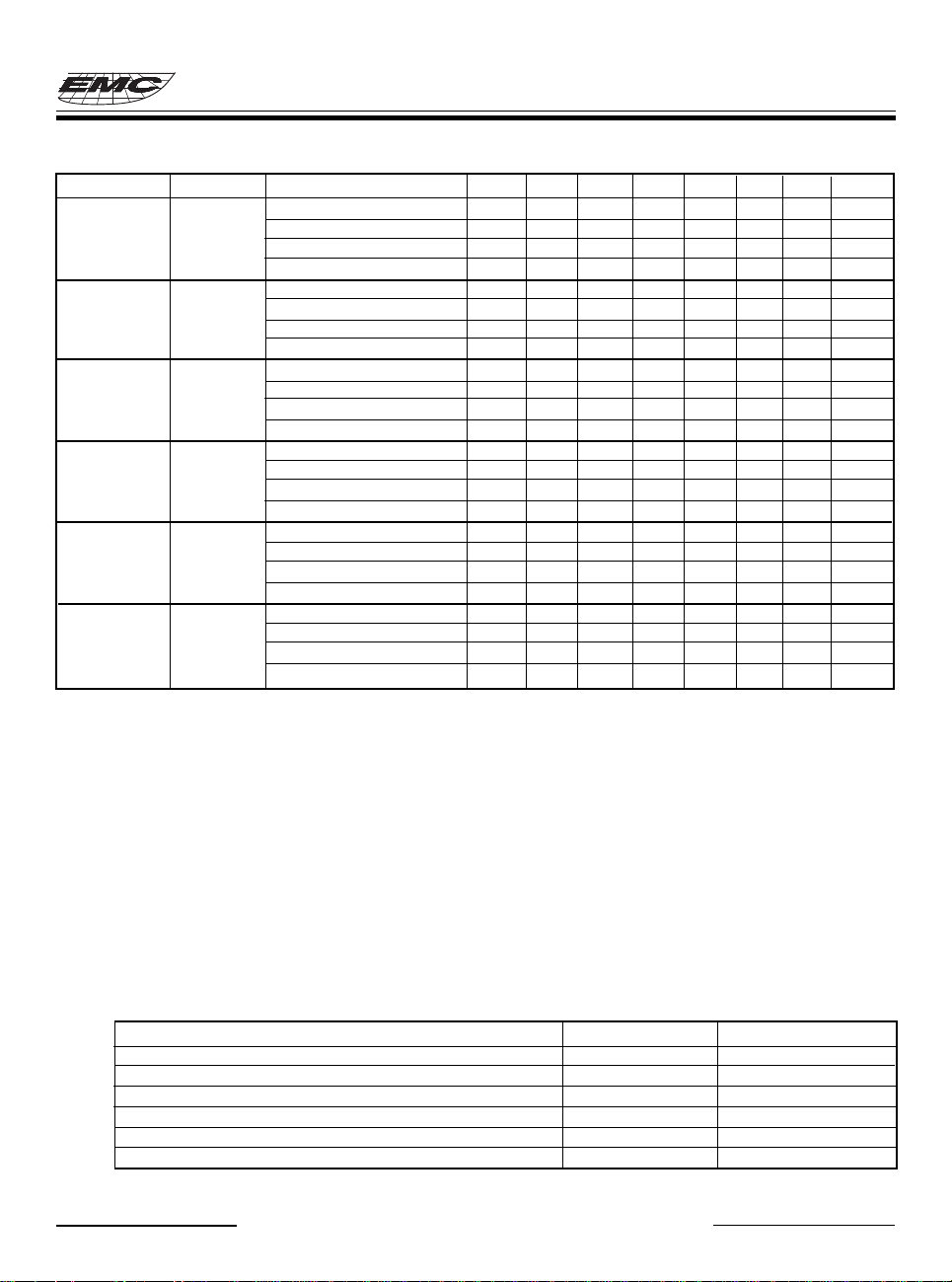
Table 3 The summary of the initialized values for registers
Address Name Reset Type Bit 7 Bit 6 Bit 5 Bit 4 Bit 3 Bit 2 Bit 1 Bit 0
Bit Name X X X X C53 C52 C51 C50
N/A IOC5 Power-on U U U U 1 1 1 1
/RESET and WDT U U U U 1 1 1 1
Wake-up from Pin Changed U U U U P P P P
Bit Name C67 C66 C65 C64 C63 C62 C61 C60
N/A IOC6 Power-on 1 1 1 1 1 1 1 1
/RESET and WDT 1 1 1 1 1 1 1 1
Wake-up from Pin Changed P P P P P P P P
Bit Name X /INT TS TE PAB PSR2 PSR1 PSR0
N/A CONT Power-on 1 0 1 1 1 1 1 1
/RESET and WDT 1 0 1 1 1 1 1 1
Wake-up from Pin Changed P P P P P P P P
Bit Name - - - - - - - -
0X00 R0(IAR) Power-on U U U U UUUU
/RESET and WDT P P P P P P P P
Wake-up from Pin Changed P P P P P P P P
Bit Name - - - - - - - -
0X01 R1(TCC) Power-on 0 0 0 0 0 0 0 0
/RESET and WDT 0 0 0 0 0 0 0 0
Wake-up from Pin Changed P P P P P P P P
Bit Name - - - - - - - -
0X02 R2(PC) Power-on 0 0 0 0 0 0 0 0
/RESET and WDT 0 0 0 0 0 0 0 0
Wake-up from Pin Changed **0/P **0/P **0/P **0/P **1/P **0/P **0/P **0/P
Bit Name GP2 GP1 GP0 T P Z DC C
0X03 R3(SR) Power-on 0 0 0 1 1 U U U
/RESET and WDT 0 0 0 T T P P P
Wake-up from Pin Changed P P P T T P P P
Bit Name GP1 GP0 - - - - - -
0x04 R4(RSR) Power-on 1 1 U U UUUU
/RESET and WDT 1 1 P P P P P P
Wake-up from Pin Changed 1 1 P P P P P P
Bit Name X X X X P53 P52 P51 P50
0x05 R5(P5) Power-on 0 0 0 0 UUUU
/RESET and WDT 0 0 0 0 P P P P
Wake-up from Pin Changed 0 0 0 0 P P P P
Bit Name P67 P66 P65 P64 P63 P62 P61 P60
0x06 R6(P6) Power-on U U U U UUUU
/RESET and WDT P P P P P P P P
Wake-up from Pin Changed P P P P P P P P
Bit Name X X X X X EXIF ICIF TCIF
0x0F RF(ISR) Power-on U U U U U 0 0 0
/RESET and WDT U U U U U 0 0 0
Wake-up from Pin Changed U U U U U P P P
Bit Name - - - - - - - -
0x0A IOCA Power-on 1 1 1 1 1 1 1 1
/RESET and WDT 1 1 1 1 1 1 1 1
Wake-up from Pin Changed P P P P P P P P
* This specification is subject to be changed without notice. 8.11.1999
B3-14
Page 15
EM78P156E
Address Name Reset Type Bit 7 Bit 6 Bit 5 Bit 4 Bit 3 Bit 2 Bit 1 Bit 0
Bit Name /PD7 /PD6 /PD5 /PD4 X /PD2 /PD1 /PD0
0x0B IOCB Power-on 1 1 1 1 U 1 1 1
/RESET and WDT 1 1 1 1 U 1 1 1
Wake-up from Pin Changed P P P P U P P P
Bit Name OD7 OD6 OD5 OD4 OD3 OD2 OD1 OD0
0x0C IOCC Power-on 0 0 0 0 0 0 0 0
/RESET and WDT 0 0 0 0 0 0 0 0
Wake-up from Pin Changed P P P P P P P P
Bit Name /PH7 /PH6 /PH5 /PH4 /PH3 /PH2 /PH1 /PH0
0x0D IOCD Power-on 1 1 1 1 1 1 1 1
/RESET and WDT 1 1 1 1 1 1 1 1
Wake-up from Pin Changed P P P P P P P P
Bit Name WDTC EIS X ROC X X X X
0x0E IOCE Power-on 1 0 U 0 U U U U
/RESET and WDT 1 0 U 0 U U U U
Wake-up from Pin Changed 1 P U P U U U U
Bit Name X X X X X EXIE ICIE TCIE
0x0F IOCF Power-on U U U U U 0 0 0
/RESET and WDT U U U U U 0 0 0
Wake-up from Pin Changed U U U U U P P P
Bit Name - - - - - - - -
0x10 R10~R3F Power-on U U U U U U U U
~ 0x3F /RESET and WDT P P P P P P P P
Wake-up from Pin Changed P P P P P P P P
** To jump address 0x08, or to execute the instruction which is next to the “SLEP” instruction.
X: not used. U: unknown or don’t care. P: previous value before reset.
t: check Table 4
2. The status of T and P of STATUS register
A RESET condition can be caused by the following events:
1. a power-on condition,
2. a high-low-high pulse on /RESET pin, and
3. Watchdog Timer time-out.
The values of T and P, listed in Table 4 can be used to check how the processor wakes up. Table 5 shows the events which
may affect the status of T and P .
Table 4 The values of T and P after RESET
Reset Type T P
Power-on 1 1
/RESET during operating mode *P *P
/RESET wake-up during SLEEP mode 1 0
WDT during operating mode 0 P
WDT wake-up during SLEEP mode 0 0
Wake-up on pin changed during SLEEP mode 1 0
*P: Previous status before reset
* This specification is subject to be changed without notice. 8.11.1999
B3-15
Page 16
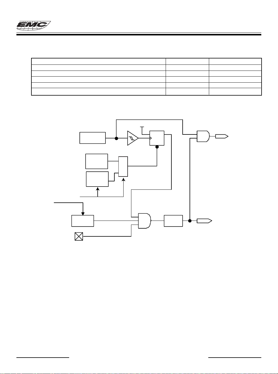
Table 5 The status of T and P being affected by events
Event T P
Power-on 1 1
WDTC instruction 1 1
WDT time-out 0 *P
SLEP instruction 1 0
Wake-up on pin changed during SLEEP mode 1 0
*P: Previous value before reset
VDD
Oscillator
DQ
CLK
CLR
EM78P156E
CLK
Power-on
Reset
Voltage
Detector
CODE
Option
WDTE
WDT
/RESET
1
0
/Enable
WDT Timeout
M
U
X
18 ms
RESET
Fig. 9 Block diagram of Reset of controller
VI.6 Interrupt
EM78P156E has three falling edge interrupts listed below :
(1) TCC overflow interrupt
(2) Port 6 input status changed interrupt
(3) External interrupt [(P60//INT) pin].
Before Port 6 input status changed interrupt being enabled, reading Port 6 (e.g. “MOV R6,R6”) is necessary.
Each pin of Port 6 can have this feature if its status changed. Any pin configured as output or P60 pin configured
as /INT is excluded from this function. The Port 6 input status changed interrupt can wake up the EM78P156E from the
sleep mode if it is enabled prior to going into the sleep mode by executing SLEP. When waking up, the controller will
continue to execute the succesive address if the global interrupt is disabled or branch to the interrupt vector 008H if the
global interrupt is enabled.
RF is the interrupt status register, which records the interrupt requests in the relative flags/bits. IOCF is an
interrupt mask register. The global interrupt is enabled by the ENI instruction and is disabled by the DISI
instruction. When one of the interrupts (when enabled) occurs, the next instruction will be fetched from address
* This specification is subject to be changed without notice. 8.11.1999
B3-16
Page 17
EM78P156E
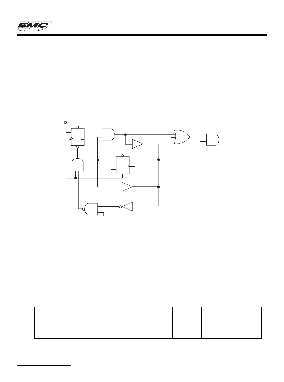
008H. Once in the interrupt service routine, the source of an interrupt can be determined by polling the flag bits
in RF. The interrupt flag bit must be cleared by instructions before leaving the interrupt service routine and
enabling interrupts to avoid recursive interrupts.
The flag (except ICIF bit) in the Interrupt Status Register (RF) is set regardless of the status of its mask bit or the
execution of ENI. Note that the outcome of RF will be the logic AND of RF and IOCF. Refer to Fig.10. The
RETI instruction ends the interrupt routine and enables the global interrupt (the execution of ENI).
When an interrupt is generated by the INT instruction (when enabled), the next instruction will be fetched from
address 001H
VCC
/IRQn
RF
/RESET
P
D
Q
CLK
R
C
Q
L
Q
Q
IOCF
P
R
CLK
C
L
RFWR
RPRD
D
IOCFWR
IOCFRD
IRQn
IRQm
.
.
ENI/DISI
IOD
/INT
Fig. 10 Interrupt input circuit
VI.7 Oscillator
1. Oscillator Modes
EM78P156E can be operated in four different oscillator modes. There are Internal Capacitor oscillator mode (IRC),
External RC oscillator mode (ERC), High XTAL oscillator mode (HXT) and Low XTAL oscillator mode (LXT). Users
can select one of them by programming MS and HLF in the CODE option register. Table 6 depicts how these four modes
to be defined.
The up-limited operation frequency of crystal/resonator on the different VDDs is listed in Table 7.
Table 6 Oscillator Modes defined by MS, HLF, HLP and IRCEN
Mode MS HLF HLP IRCEN
External RC oscillator mode 0 *X *X 1
High XTAL oscillator mode 1 1 *X *X
Low XTAL oscillator mode 1 0 0 *X
Internal C, External R oscillator mode 0 *X *X 0
<Note> 1. X, Do not care
2. The transient point of system frequency between HXT and LXY is around 400 KHz.
* This specification is subject to be changed without notice. 8.11.1999
B3-17
Page 18
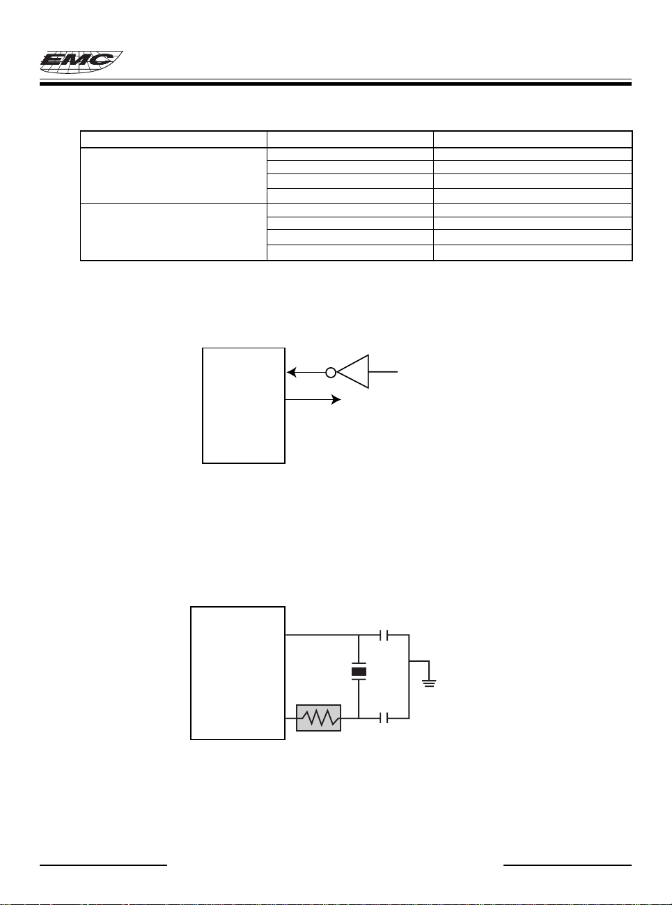
Table 7 The summary of maximum operating speeds
Conditions VDD (V) Fxt max. (MHz)
2.5 8
Two clocks 3 12
518
6.4 20
2.5 16
Four clocks 3 24
536
6.5 40
2. Crystal Oscillator/Ceramic Resonators (XTAL)
EM78P156E can be driven by an external clock signal through the OSCI pin as shown in Fig.11
EM78P156E
OSCI
Ext. Clock
OSCO
EM78P156E
Fig. 11 Circuit for External Clock Input
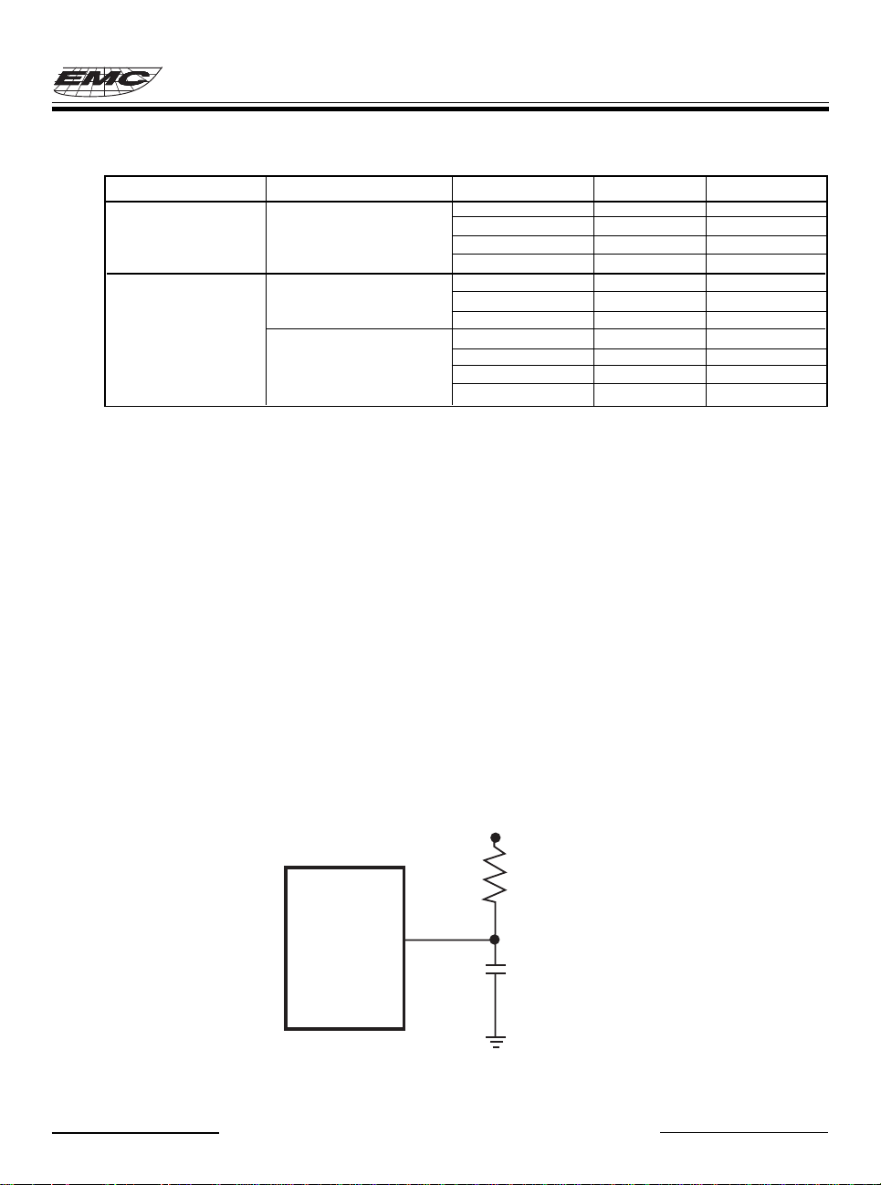
In the most applications, pin OSCI and pin OSCO can be connected with a crystal or ceramic resonator to generate
oscillation. Fig.12 depicts the circuit. It is the same no matter in the HXT mode or in the LXT mode. Table 8
recommends the values of C1 and C2. Since each resonator has its own attribute, users should refer to their specifications
for appropriate values of C1 and C2. RS, a serial resistor, may be necessary for AT strip cut crystal or low frequency
mode
C1
OSCI
EM78P156E
XTAL
OSCO
RS
Fig. 12 Circuit for Crystal/Resonator
C2
* This specification is subject to be changed without notice. 8.11.1999
B3-18
Page 19
EM78P156E
Table 8 Capacitor Selection Guide for Crystal Oscillator or Ceramic Resonators
Oscillator Type Frequency Mode Frequency C1 (pF) C2 (pF)
455 KHz 100~150 100~150
1.00 MHz 40~80 40~80
Ceramic Resonator HXT 2.0 MHz 20~40 20~40
4.0 MHz 10~30 10~30
32.768 KHz 25 15
LXT 100 KHz 25 25
200 KHz 25 25
Crystal Oscillator 455 KHz 20~40 20~150
HXT 1.0 MHz 15~30 15~30
2.0 MHz 15 15
4.0 MHz 15 15
3. ERC Oscillator Mode
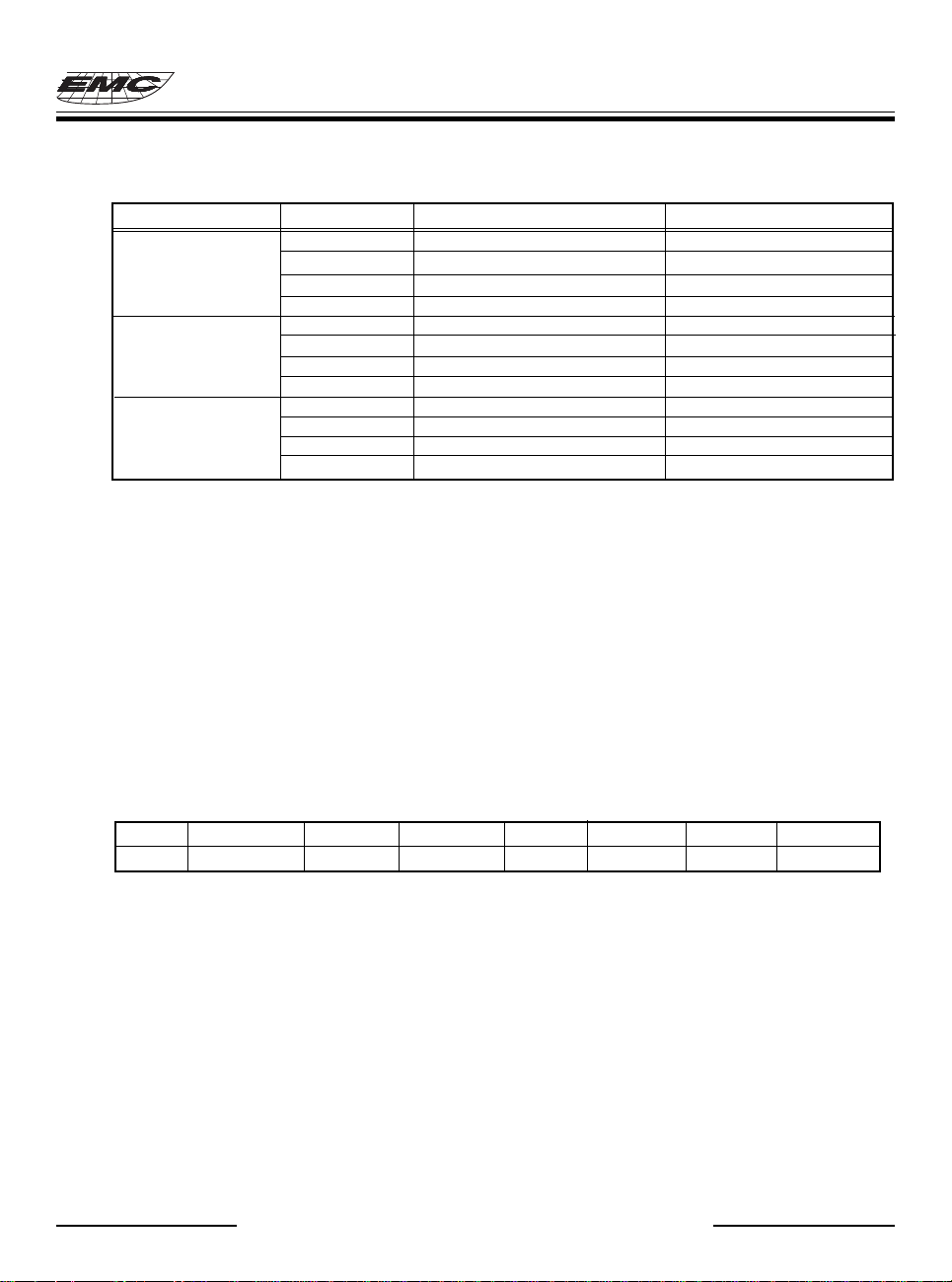
For some applications whose timing need not be calculated precisely, the RC oscillator (Fig.13) offers a lot of cost
savings. Nevertheless, it should be aware that the frequency of the RC oscillator is the function of the supply voltage,
the values of the resistor (Rext), the capacitor (Cext), and even the operation temperature.
Moreover to this, the frequency also changes slightly from one chip to another due to the process variation.
In order to maintain a stable system frequency, the values of the Cext should not be less than 20pF as well as the
value of Rext should not be greater than 1M ohm. If they can not be kept in this range, the frequency is affected easily
by noise, humidity and leakage.
The smaller Rext the RC oscillator has, the faster frequency it gets. On the contrary, for very low Rext values,
for instance, 1KΩ, the oscillator becomes unstable because the NMOS can not discharge the current of the
capacitance correctly.
On a basis of the above reasons, it must be kept in mind that all of the supply voltage, the operation temperature, the
components of the RC oscillator, the package types and the ways of PCB layout will effect the system frequency.
V
CC
Rext
OSCI
EM78P156E
Fig. 13 Circuit for External RC Oscillator Mode
* This specification is subject to be changed without notice. 8.11.1999
B3-19
Cext
Page 20
EM78P156E
Table 9 RC Oscillator Frequencies
Cext Rext Average Fosc @ 5V, 25°C Average Fosc @ 3V, 25°C
3.3k 3.92 MHz 3.65 MHz
20pF
100pF
300pF
* 1. Measured on DIP packages.
2. Design reference only
4. IRC Oscillator Mode
In IRC mode, it consists of an internal C which default frequency value is 4MHz. We suggest that the external Resistant
value here should be 50KΩ connected to vdd with internal C.
5.1k 2.67 MHz 2.60 MHz
10k 1.39 MHz 1.40 MHz
100k 1.49 KHz 156 KHz
3.3k 1.39 MHz 1.33 MHz
5.1k 940 KHz 920 KHz
10k 480 KHz 475 KHz
100k 52 KHz 50 KHz
3.3k 595 KHz 560 KHz
5.1k 400 KHz 390 KHz
10k 200 KHz 200 KHz
100k 21 KHz 20 KHz
VI.8 CODE Option Register
1. Code Option Register
The EM78P156E has one Code option register which is not a part of the normal program memory. The option bits
can not be accessed during normal program execution.
12 11 10 9 8 7 6 5~0
MS ENWDTB CLKS PTB HLF IRCEN HLP ------
Bit 12 (MS): Oscillator type selection.
0: RC type
1: XTAL type (XTAL1 and XTAL2)
Bit 11 (ENWDTB): Watchdog Timer enable.
0: Enable
1: Disable
Bit 10 (CLKS): Instruction period option.
0: two oscillator periods
1: four oscillator periods
Refer to the section of Instruction Set.
Bit 9 (PTB): Protect bit
0: Enable
1: Disable
Bit 8 (HLF): XTAL frequency selection.
0: XTAL2 type (Low frequency, 32.768KHz)
* This specification is subject to be changed without notice. 8.11.1999
B3-20
Page 21
EM78P156E
1: XTAL1 type (High frequency)
This bit will affect system oscillation only when Bit 12 (MS) is “1”. When MS is “0”, HLF must be “0”.
Bit 7 (IRCEN): RC oscillator selection.
0: R connected to Vdd with internal C.
1: External RC
Bit 6 (HLP): Power selection.
0: Low power
1: High power
Bits 5 ~ 0: Not used.
2. User’s ID Register
The EM78P156E has one User’s ID register which is not a part of the normal program memory. The User’s ID bits
can not be accessed during normal program execution.
12 ~0
XXXXXXXXXXXXX
Bit 12 ~ 0: User’s ID code.
VI.9 Power-on Considerations
Any microcontroller is not warranted to start proper operation before the power supply stays in its steady state.
EM78P156E is equipped with Power On Voltage Detector (POVD) which the detective level is about 1.8V. It
will work well if Vdd rises quickly enough (50ms or less). In many critical applications; however, extra devices
are still required to assist in solving power-up problems.
VI.10 External Power-on Reset Circuit
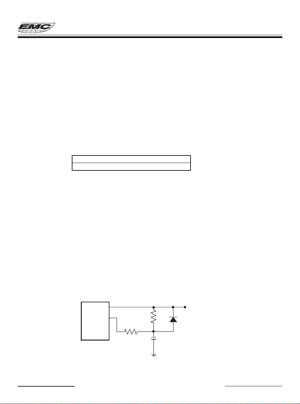
The circuit shown in Fig.14 implements an external RC to produce the reset pulse. The pulse width (time constant)
should keep long enough until Vdd has reached minimum operation voltage. This circuit is used when the power supply
has slow rise time. Because the current leakage from the /RESET pin is about 5A, it is recommended that R should
not be greater than 40K. In this way, the voltage in pin /RESET will be held below 0.2V. The diode (D) acts a short circuit
at the moment of power-down. The capacitor, C, will be discharged rapidly and fully. Rin, the current-limited resistor,
protects against a high discharging current or ESD (electrostatic discharge) flowing to pin /RESET.
VDD
/RESET
EM78P156E
Rin
Fig. 14 External Power-up Reset Circuit
R
C
D
* This specification is subject to be changed without notice. 8.11.1999
B3-21
Page 22
EM78P156E
VI.11 Residue Voltage Protection
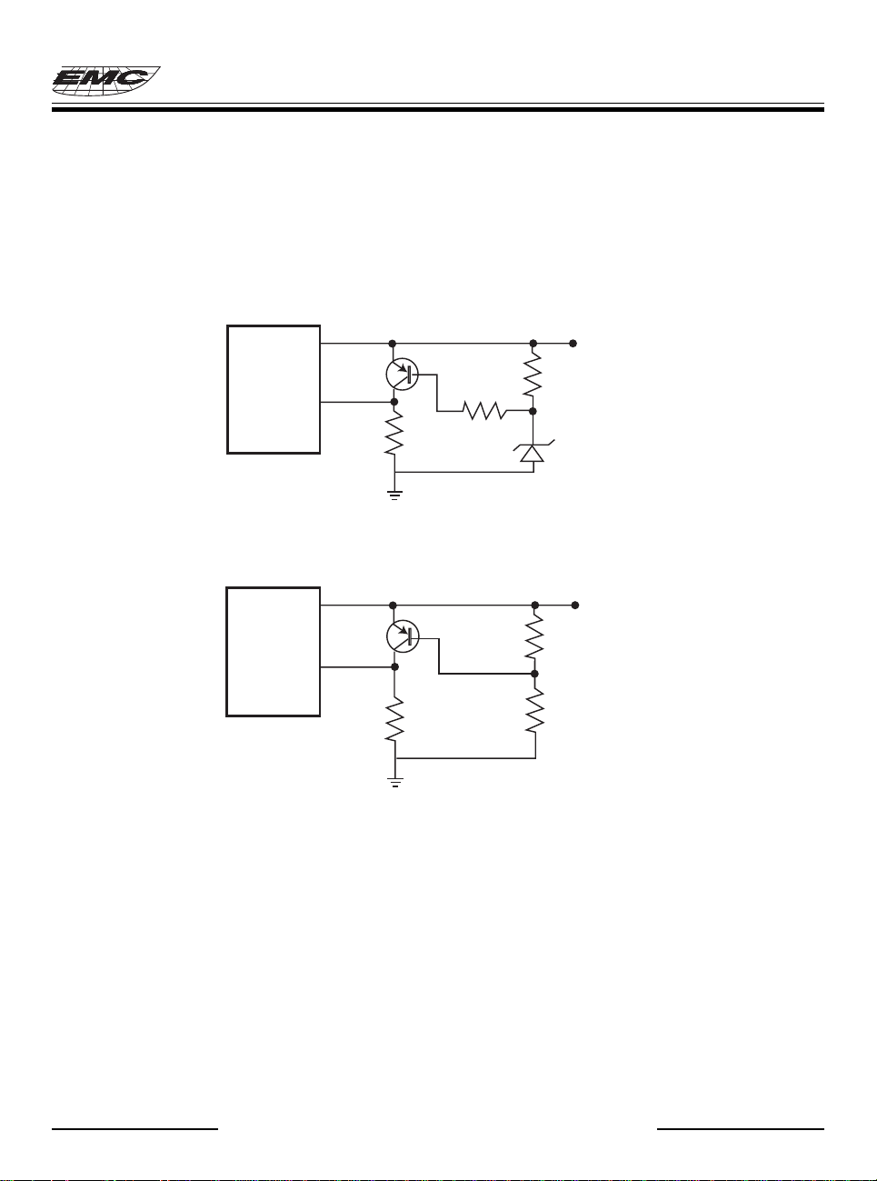
In some applications, replacing battery as an instance, device power (Vdd) is taken off and recovered within a few
seconds. A residue voltage, which trips below Vdd min but not to zero, may exist. This condition may cause a poor
power-on reset. Fig.15 and Fig.16 show how to build the residue voltage protection circuit
VDD
EM78P156E
/RESET
Fig. 15 Circuit 1 for the residue voltage protection
VDD
EM78P156E
/RESET
Fig. 16 Circuit 2 for the residue voltage protection
Q1
100K
Q1
R3
10K
IN4684
R1
R2
VDD
33K
VDD
* This specification is subject to be changed without notice. 8.11.1999
B3-22
Page 23

EM78P156E
VI.12 Instruction Set
Each instruction in the instruction set is a 13-bit word divided into an OP code and one or more operands.
Normally, all instructions are executed within one single instruction cycle (one instruction consists of 2 oscillator
periods), unless the program counter is changed by instruction “MOV R2,A”, “ADD R2,A”, or instructions of arithmetic
or logic operation on R2 (e.g. “SUB R2,A”, “BS(C) R2,6”, “CLR R2”, ......). In this case, the execution takes two
instruction cycles.
Under some conditions, if the specification of the instruction cycle is not suitable for some applications, they can be
modified as follows:
(A) one instruction cycle consists of 4 oscillator periods.
(B) “JMP”, “CALL”, “RET”, “RETL”, “RETI”, and the conditional skip (“JBS”, “JBC”, “JZ”, “JZA”, “DJZ”,
“DJZA”) tested to be true are executed within two instruction cycles. The instructions that write to the program
counter also take two instruction cycles.
The Case (A) is selected by the CODE option bit, called CLKS. One instruction cycle consists of two oscillator
clocks if CLKS is low, and consists of four oscillator clocks if CLKS is high.
Note that once 4 oscillator periods within one instruction cycle is selected in Case (A), the internal clock source to
TCC is CLK=Fosc/4 instead of Fosc/ 2 that is shown in Fig.5.
In addition, the instruction set has the following features:
(1) Every bit of any register can be set, cleared or tested directly.
(2) The I/O registers can be regarded as general registers. That is, the same instruction can operate on I/O register.
The symbol “R” represents a register designator which specifies which one of the registers (including operational
registers and general-purpose registers) to be utilized by the instruction. The symbol “b” represents a bit field designator
which selects the number of the bit located in the register “R” affected by the operation. The symbol “k” represents an
8 or 10-bit constant or literal value.
* This specification is subject to be changed without notice. 8.11.1999
B3-23
Page 24
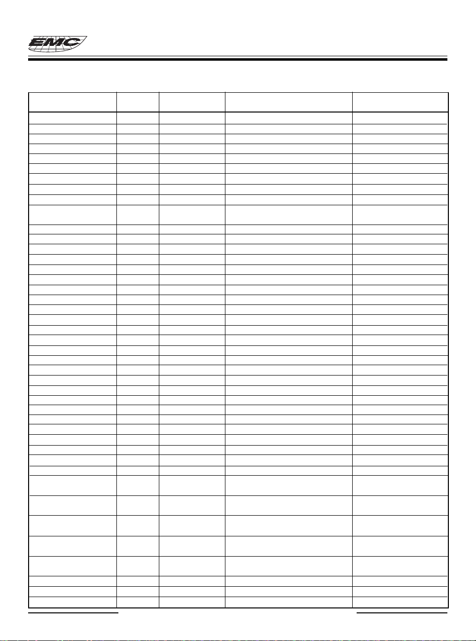
EM78P156E
Table 10 The list of the instruction set of EM78P156E
INSTRUCTION HEX MNEMONIC OPERATION STATUS
BINARY AFFECTED
0 0000 0000 0000 0000 NOP No Operation None
0 0000 0000 0001 0001 DAA Decimal Adjust A C
0 0000 0000 0010 0002 CONTW A → CONT None
0 0000 0000 0011 0003 SLEP 0 → WDT, Stop oscillator T,P
0 0000 0000 0100 0004 WDTC 0 → WDT T,P
0 0000 0000 rrrr 000r IOW R A → IOCR None <Note1>
0 0000 0001 0000 0010 ENI Enable Interrupt None
0 0000 0001 0001 0011 DISI Disable Interrupt None
0 0000 0001 0010 0012 RET [Top of Stack] → PC None
0 0000 0001 0011 0013 RETI [Top of Stack] → PC, None
Enable Interrupt
0 0000 0001 0100 0014 CONTR CONT → A None
0 0000 0001 rrrr 001r IOR R IOCR → A None <Note1>
0 0000 01rr rrrr 00rr MOV R,A A → R None
0 0000 1000 0000 0080 CLRA 0 → AZ
0 0000 11rr rrrr 00rr CLR R 0 → RZ
0 0001 00rr rrrr 01rr SUB A, R R-A → A Z,C,DC
0 0001 01rr rrrr 01rr SUB R,A R-A → R Z,C,DC
0 0001 10rr rrrr 01rr DECA R R-1 → AZ
0 0001 11rr rrrr 01rr DEC R R-1 → RZ
0 0010 00rr rrrr 02rr OR A,R A ∨ VR → AZ
0 0010 01rr rrrr 02rr OR R,A A ∨ VR → RZ
0 0010 10rr rrrr 02rr AND A,R A & R → AZ
0 0010 11rr rrrr 02rr AND R,A A & R → RZ
0 0011 00rr rrrr 03rr XOR A,R A ⊕ R → AZ
0 0011 01rr rrrr 03rr XOR R,A A ⊕ R → RZ
0 0011 10rr rrrr 03rr ADD A,R A + R → A Z,C,DC
0 0011 11rr rrrr 03rr ADD R,A A + R → R Z,C,DC
0 0100 00rr rrrr 04rr MOV A,R R → AZ
0 0100 01rr rrrr 04rr MOV R,R R → RZ
0 0100 10rr rrrr 04rr COMA R /R → AZ
0 0100 11rr rrrr 04rr COM R /R → RZ
0 0101 00rr rrrr 05rr INCA R R+1 → AZ
0 0101 01rr rrrr 05rr INC R R+1 → RZ
0 0101 10rr rrrr 05rr DJZA R R-1 → A, skip if zero None
0 0101 11rr rrrr 05rr DJZ R R-1 → R, skip if zero None
0 0110 00rr rrrr 06rr RRCA R R(n) → A(n-1)
R(0) → C, C → A(7) C
0 0110 01rr rrrr 06rr RRC R R(n) → R(n-1)
R(0) → C, C → R(7) C
0 0110 10rr rrrr 06rr RLCA R R(n) → A(n+1)
R(7) → C, C → A(0) C
0 0110 11rr rrrr 06rr RLC R R(n) → R(n+1)
R(7) → C, C → R(0) C
0 0111 00rr rrrr 07rr SWAPA R R(0-3) → A(4-7)
R(4-7) → A(0-3) None
0 0111 01rr rrrr 07rr SWAP R R(0-3) ↔ R(4-7) None
0 0111 10rr rrrr 07rr JZA R R+1 → A, skip if zero None
0 0111 11rr rrrr 07rr JZ R R+1 → R, skip if zero None
* This specification is subject to be changed without notice. 8.11.1999
B3-24
Page 25
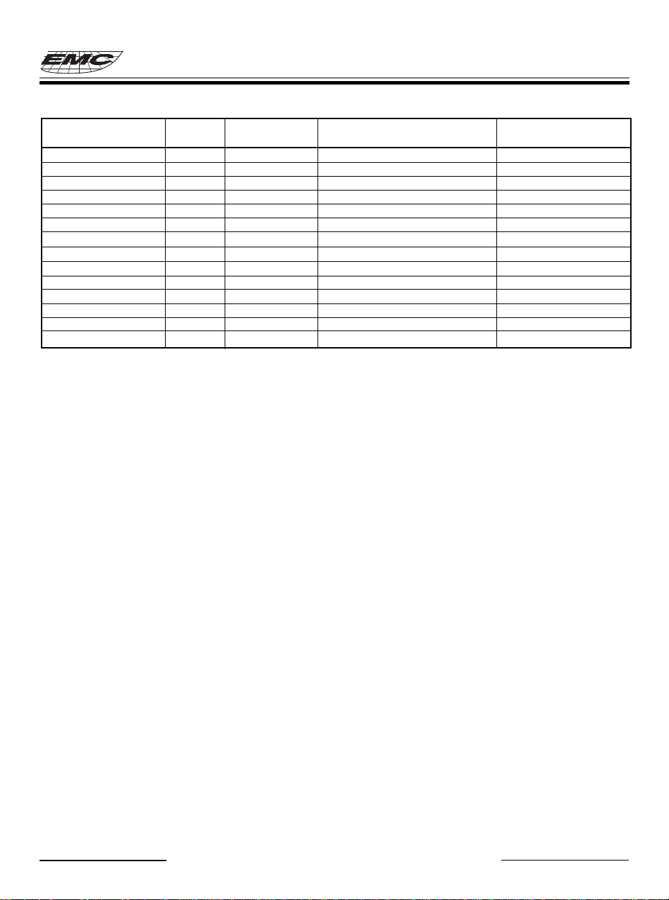
EM78P156E
INSTRUCTION HEX MNEMONIC OPERATION STATUS
BINARY AFFECTED
0 100b bbrr rrrr 0xxx BC R,b 0 → R(b) None <Note2>
0 101b bbrr rrrr 0xxx BS R,b 1 → R(b) None <Note3>
0 110b bbrr rrrr 0xxx JBC R,b if R(b)=0, skip None
0 111b bbrr rrrr 0xxx JBS R,b if R(b)=1, skip None
1 00kk kkkk kkkk 1kkk CALL k PC+1 → [SP], (Page, k) → PC None
1 01kk kkkk kkkk 1kkk JMP k (Page, k) → PC None
1 1000 kkkk kkkk 18kk MOV A,k k → A None
1 1001 kkkk kkkk 19kk OR A,k A ∨ k → AZ
1 1010 kkkk kkkk 1Akk AND A,k A & k → AZ
1 1011 kkkk kkkk 1Bkk XOR A,k A ⊕ k → AZ
1 1100 kkkk kkkk 1Ckk RETL k k → A, [Top of Stack] → PC None
1 1101 kkkk kkkk 1Dkk SUB A,k k-A → A Z,C,DC
1 1110 0000 0001 1E01 INT PC+1 → [SP], 001H → PC None
1 1111 kkkk kkkk 1Fkk ADD A,k k+A → A Z,C,DC
<Note 1> This instruction can operate on IOC5~IOC6, IOCA~IOCF only.
<Note 2> This instruction is not recommended to operate on RF.
<Note 3> This instruction cannot operate on RF.
* This specification is subject to be changed without notice. 8.11.1999
B3-25
Page 26
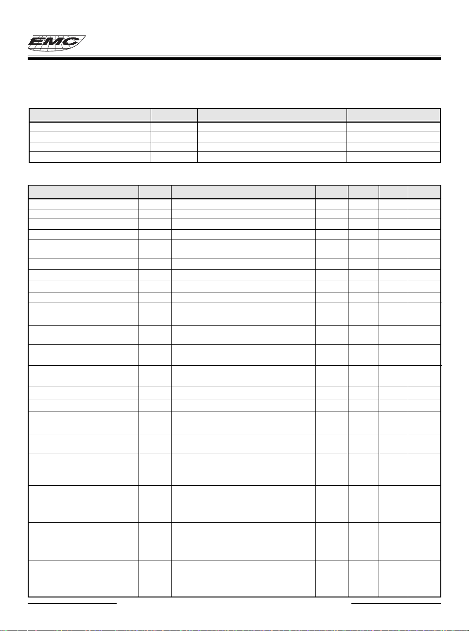
EM78P156E
VII. ABSOLUTE MAXIMUM RATINGS
Items Sym. Condition Rating
Temperature under bias T
Storage temperature T
Input voltage V
Output voltage V
OPR
STR
IN
O
VIII. DC ELECTRICAL CHARACTERISTIC (Ta=0°C ~ 70°C, V
Parameter Sym. Condition Min. Typ. Max. Unit
XTAL : VDD to 3V Fxt Two cycles with two clocks DC 12.0 MHz
XTAL : VDD to 5V Fxt DC 18.0 MHz
ERC : VDD to 5V F
IRC : VDD to 5V F
Input Leakage Current I
for input pins
Input High Voltage V
Input Low Voltage V
Input High Threshold Voltage V
Input Low Threshold Voltage V
Clock Input High Voltage V
Clock Input Low Voltage V
Output High Voltage V
(Port 5,6)
Output Low Voltage V
(P50~P53,P62~P67)
Output Low Voltage V
(P60,P61)
Pull-high current I
Pull-down current I
Power-down current I
Power-down current I
Operating supply current I
=3V) type, CLKS="0"), output pin floating, 15 15 30 µA
(V
DD
at two cycles/two clocks WDT disabled
Operating supply current I
=3V) type,CLKS="0"), output pin floating, 20 35 µA
(V
DD
RC
RC
IL
IH
IL
IHT
ILT
IHX
ILX
OH1
OL1
OL2
PH
PD
SB1
SB2
CC1
CC2
at two cycles/two clocks WDT enabled
Operating supply current I
(V
=5V) type,CLKS="0"), output pin floating 1.6 mA
DD
CC3
at two cycles/two clocks WDT enable
Operating supply current I
=5V) type,CLKS="0"), output pin floating 4 mA
(V
DD
CC4
at two cycles/two clocks WDT enable
* This specification is subject to be changed without notice. 8.11.1999
R : 5.1KΩ , C : 100pF F±20% 760 F±20% KHz
R : 50KΩ F±20% 4 F±20% MHz
V
= VDD, V
IN
SS
Ports 5, 6 2.0 V
Ports 5, 6 0.8 V
/RESET, TCC 2.0 V
/RESET, TCC 0.8 V
OSCI 3.5 V
OSCI 1.5 V
I
= -12mA 2.4 V
OH
IOL = 10.5mA 0.4 V
I
= 12mA 0.4 V
OL
Pull-high active, input pin at V
Pull-down active, input pin at V
SS
DD
-50 -70 -240 µA
25 50 120 µA
All input and I/O pins at VDD, output 1 µA
pin floating, WDT disabled
All input and I/O pins at VDD, output 10 µA
pin floating, WDT enabled
/RESET='High', Fosc=32KHz(Crystal
/RESET='High', Fosc=32KHz(Crystal
/RESET='High', Fosc=4MHz (Crystal
/RESET='High', Fosc=10MHz (Crystal
B3-26
0°C to 70°C
-65°C to 150°C
-0.3V to +6.0V
-0.3V to +6.0V
=5.0V±5%, VSS=0V)
DD
±1 µA
Page 27
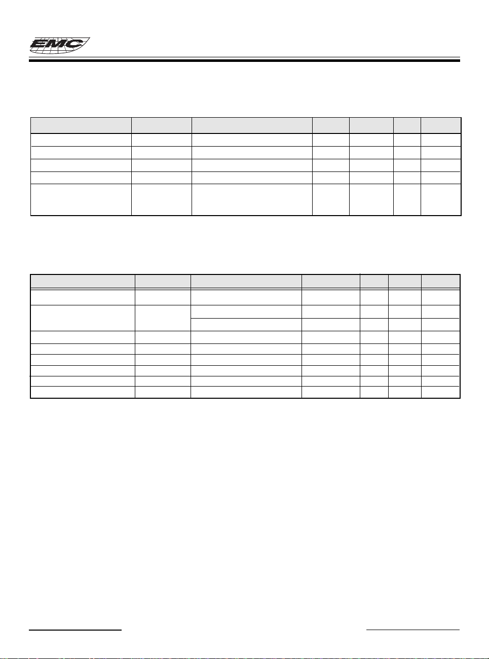
EM78P156E
IX. VOLTAGE DETECTOR ELECTRICAL CHARACTERISTIC (Ta = 25°C)
Parameter Symbol Condition Min. Typ. Max. Unit
Detect voltage Vdet 1.7 1.8 1.9 V
Release voltage Vrel Vdet x1.05 V
Current consumption Iss V
Operating voltage Vop 0.7* 5.5 V
Temperature ∆Vdet/ 0°C ≤Ta≤ 70°C -2 mV/°C
characteristic of Vdet ∆Ta
= 5V 5 µA
DD
X. AC ELECTRICAL CHARACTERISTICS (Ta=0°C ~ 70°C, V
Parameter Symbol Condition Min. Typ. Max. Unit
Input CLK duty cycle Dclk 45 50 55 %
Instruction cycle time Tins XTAL Type 125 DC ns
(CLKS="0") RC Type 500 DC ns
TCC input period Ttcc (Tins+20)/N* ns
Device reset hold time Tdrh Ta = 25°C 16.8 ms
Watchdog Timer period Twdt Ta = 25°C 16.8 ms
Input pin setup time Tset 0 ns
Input pin hold time Thold 20 ns
Output pin delay time Tdelay Cload=20pF 50 ns
Note : N*= selected prescaler ratio.
=5.0V±5%, VSS=0V)
DD
* This specification is subject to be changed without notice. 8.11.1999
B3-27
Page 28
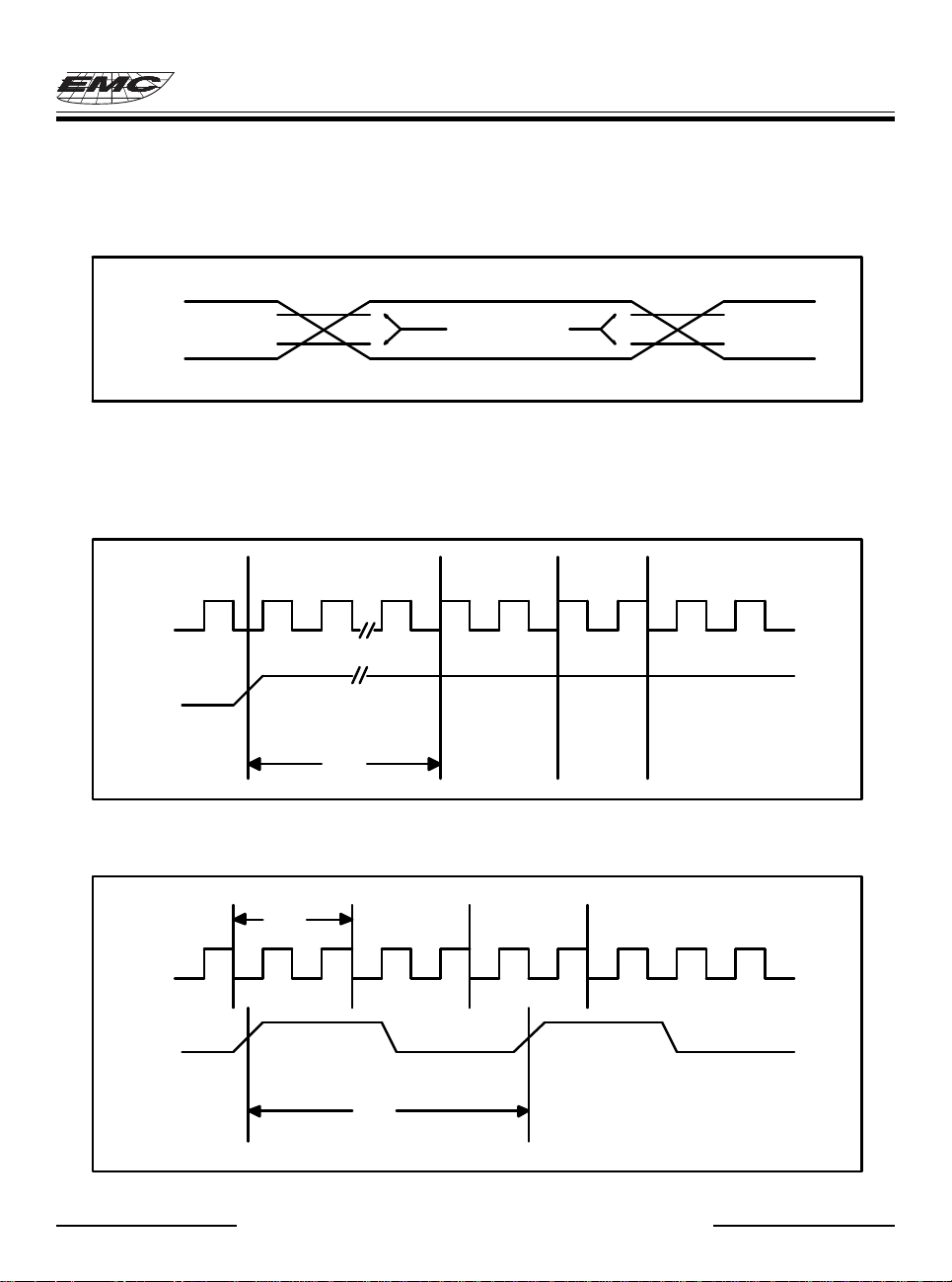
XI. TIMING DIAGRAMS
AC Test Input/Output Waveform
EM78P156E
2.4
0.45
2.0
0.8
TEST PONITS
2.0
0.8
AC Testing : Input is driven at 2.4V for logic "1", and 0.45V for logic "0". Timing
measurements are made at 2.0V for logic "1", and 0.8V for logic "0".
RESET Timing (CLK="0")
NOP
CLK
/RESET
Tdrh
Instruction 1
Executed
TCC Input Timing (CLK="0")
CLK
TCC
Tins
Ttcc
* This specification is subject to be changed without notice. 8.11.1999
B3-28
 Loading...