

Datasheet EM658160TS-8, EM658160TS-7, EM658160TS-6, EM658160TS-5, EM658160TS-4 Datasheet (ETRON)
...Page 1
Etr onT ech
EM658160
4M x 16 DDR Synchronous DRAM (SDRAM)
Etron Confidential (Rev. 1.1 Jan./2002)
Features
•
Fast clock rate: 300/285/250/200/166/143/125MHz
•
Differential Clock CK & /CK
•
Bi-directional DQS
•
DLL enable/disable by EMRS
•
Fully synchronous operation
•
Internal pipeline architecture
•
Four internal banks, 1M x 16-bit for each bank
•
Programmable Mode and Extended Mode registers
- /CAS Latency: 2, 2.5, 3
- Burst length: 2, 4, 8
- Burst Type: Sequential & Interleaved
•
Individual byte write mask control
•
DM Write Latency = 0
•
Auto Refresh and Self Refresh
•
4096 refresh cycles / 64ms
•
Precharge & active power down
•
Power supplies: V
•
Interface: SSTL_2 I/O Interface
•
Package: 66 Pin TSOP II, 0.65mm pin pitch
= 3.3V ± 0.3V
DD
= 2.5V ± 0.2V
V
DDQ
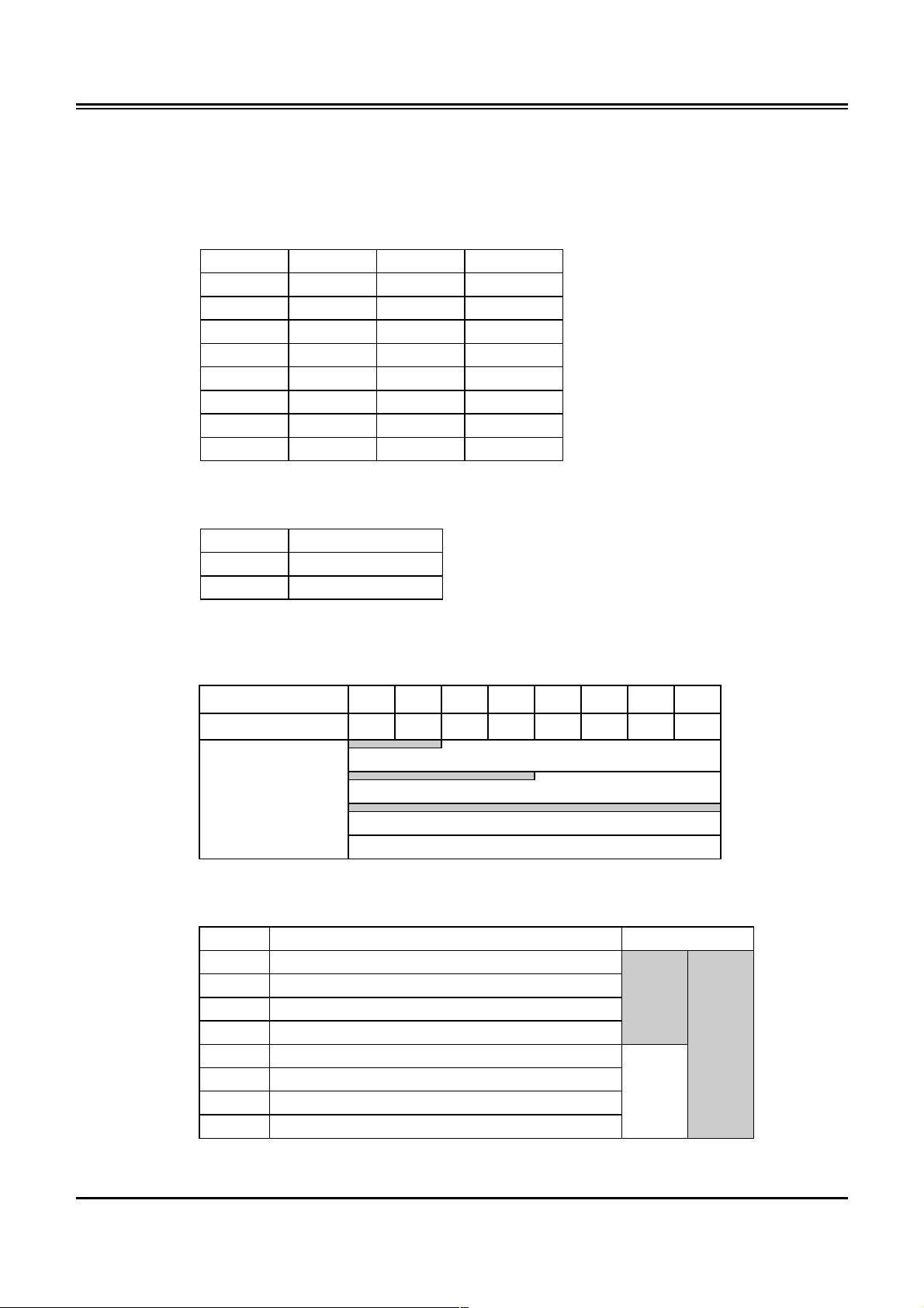
Ordering Information
Part Number Frequency Package
EM658160TS-3.3 300MHz TSOP II
EM658160TS-3.5 285MHz TSOP II
EM658160TS-4 250MHz TSOP II
EM658160TS-5 200MHz TSOP II
EM658160TS-6 166MHz TSOP II
EM658160TS-7 143MHz TSOP II
EM658160TS-8 125MHz TSOP II
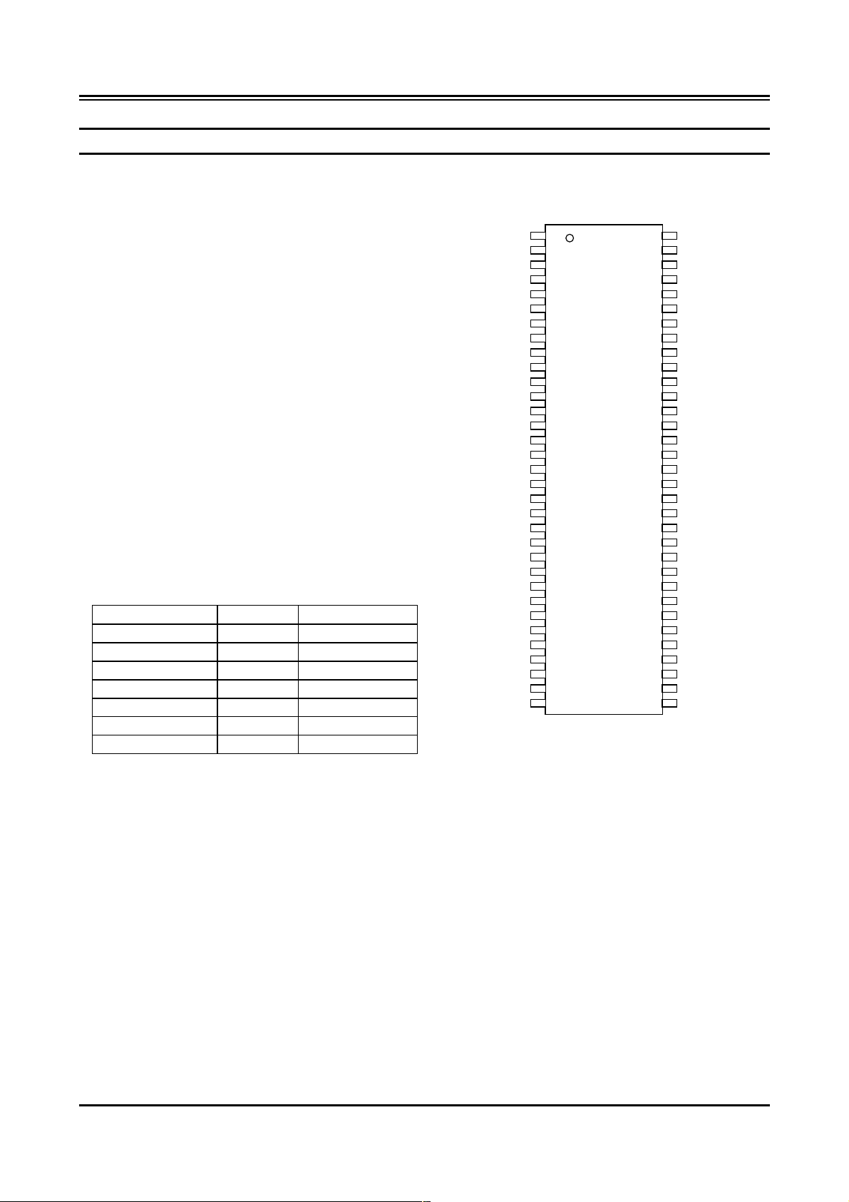
Pin Assignment (Top View)
VDD
DQ0
VDDQ
DQ1
DQ2
VSSQ
DQ3
DQ4
VDDQ
DQ5
DQ6
VSSQ
DQ7
NC
VDDQ
LDQS
NC
VDD
NC
LDM
/WE
/CAS
/RAS
/CS
NC
BS0
BS1
A10/AP
VDD
1
2
3
4
5
6
7
8
9
10
11
12
13
14
15
16
17
18
19
20
21
22
23
24
25
26
27
28
29
A0
30
A1
31
A2
32
A3
33
66
65
64
63
62
61
60
59
58
57
56
55
54
53
52
51
50
49
48
47
46
45
44
43
42
41
40
39
38
37
36
35
34
VSS
DQ15
VSSQ
DQ14
DQ13
VDDQ
DQ12
DQ11
VSSQ
DQ10
DQ9
VDDQ
DQ8
NC
VSSQ
UDQS
NC
VREF
VSS
UDM
/CK
CK
CKE
NC
NC
A11
A9
A8
A7
A6
A5
A4
VSS
Overview
The EM658160 SDRAM is a high-speed CMOS
double data rate synchronous DRAM containing 64
Mbits. It is internally configured as a quad 1M x 16
DRAM with a synchronous interface (all signals are
registered on the positive edge of the clock signal, CK).
Data outputs occur at both rising edges of CK and /CK.
Read and write accesses to the SDRAM are burst
oriented; accesses start at a selected location and
continue for a programmed number of locations in a
programmed sequence. Accesses begin with the
registration of a BankActivate command which is then
followed by a Read or Write command. The EM658160
provides programmable Read or Write burst lengths of 2,
4, 8, full page.
An auto precharge function may be enabled to
provide a self-timed row precharge that is initiated at the
end of the burst sequence. The refresh functions, either
Auto or Self Refresh are easy to use. In addition,
EM658160 features programmable DLL option. By
having a programmable mode register and extended
mode register, the system can choose the most suitable
modes to maximize its performance. These devices are
well suited for applications requiring high memory
bandwidth, result in a device particularly well suited to
high performance main memory and graphics
applications.
Etron Technology, Inc.
No. 6, Technology Rd. V, Science-Based Industrial Park, Hsinchu, Taiwan 30077, R.O.C.
TEL: (886)-3-5782345 FAX: (886)-3-5778671
Etron Technology, Inc., reserves the right to make changes to its products and specifications without notice.
Page 2
Etr onT ech
h
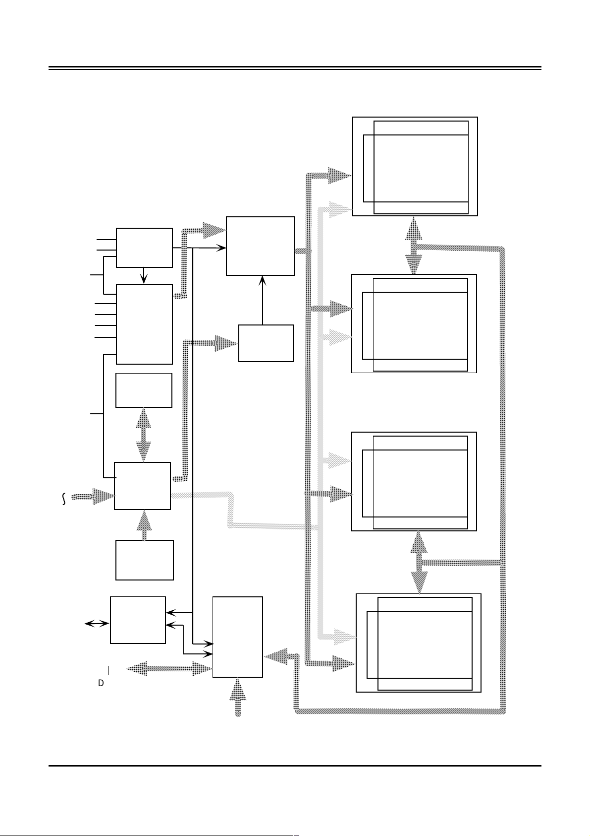
Block Diagram
4Mx16 DDR SDRAM
Row Decoder
EM658160
Column Decoder
1MX1 6
CELL ARRAY
(BANK #0)
Sense Amplifier
CK
/CK
CKE
/CS
/RAS
/CAS
/WE
A10/AP
A0
A11
BS0
BS1
DLL
CLOCK
BUFFER
COMMAND
DECODER
COLUMN
COUNTER
ADDRESS
BUFFER
CONTROL
SIGNAL
GENERATOR
MODE
REGISTER
Sense Amplifier
1MX16
CELL ARRAY
(BANK #1)
Row Decoder
Column Decoder
Column Decoder
1MX16
CELL ARRAY
(BANK #2)
Row Decoder
Sense Amplifier
REFRESH
COUNTER
Sense Amplifier
1MX1 6
CELL ARRAY
(BANK #3)
Row Decoder
Column Decoder
LDQS,
UDQS
DQ0
DQ15
DATA
STROBE
BUFFER
DQ
BUFFER
LDM, UDM
Etron Confidential 2 Rev. 1.1 Jan. 2002
Page 3
Etr onT ech
4Mx16 DDR SDRAM
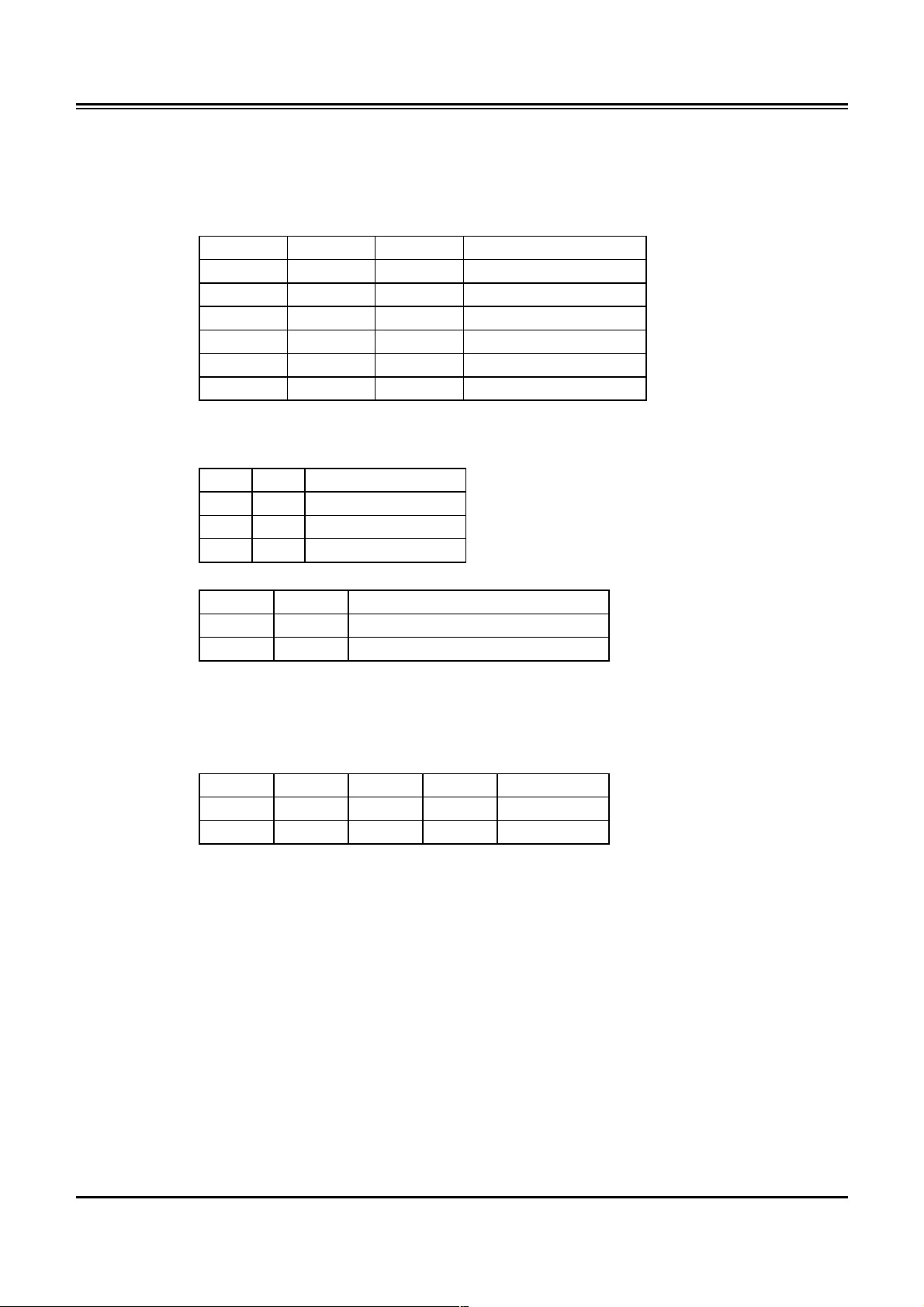
Pin Descriptions
Table 1. Pin Details of EM658160
Symbol Type Description
EM658160
CK, /CK Input
CKE Input
BS0, BS1 Input
A0-A11 Input
/CS Input
/RAS Input
Differential Clock:
are sampled on the positive edge of CK. Both CK and /CK inc r ement the internal burst
counter and controls the output registers.
Clock Enable:
goes low synchronously with clock, the internal clock is suspended f r om the next clock
cycle and the state of output and burst address is f rozen as long as the CKE rem ains
low. When all bank s are in the idle state, deactivating the cloc k controls the entry to
the Power Down and Self Refresh modes.
Bank Select:
BankPrecharge command is being applied.
Address Inputs:
address A0-A11) and Read/W rite c omm and (column address A0-A7with A10 def ining
Auto Precharge).
Chip Select:
command decoder. All commands are masked when /CS is sampled HIGH. /CS
provides for external bank selection on systems with multiple banks. It is considered
part of the command code.
Row Address Strobe:
conjunction with the /CAS and /WE signals and is latched at the positive edges of CK.
When /RAS and /CS are asserted "LOW " and /CAS is asserted "HIGH," either the
BankActivate command or the Precharge command is selected by the /WE signal.
When the /W E is asserted "HIGH," the BankActivate command is selected and the
bank designated by BS is turned on to the active state. When the /W E is asserted
"LOW," the Precharge command is selected and the bank designated by BS is
switched to the idle state after the precharge operation.
CK, /CK are driven by the system clock. All SDRAM input signals
CKE activates(HIGH) and deactivates(LOW) the CK signal. If CKE
BS0 and BS1 defines to which bank the BankActivate, Read, W rite, or
A0-A11 are sampled during the BankActivate command (row
/CS enables (sampled LOW) and disables (sampled HIGH) the
The /RAS signal defines the operation commands in
/CAS Input
/WE Input
LDQS,
UDQS
LDM,
UDM
DQ0 - DQ15 Input /
Input /
Output
Input
Output
Column Address Strobe:
conjunction with the /RAS and /WE signals and is latched at the positive edges of CK.
When /RAS is held "HIGH" and /CS is asserted "LOW ," the colum n access is started
by asserting /CAS "LOW ." T hen, the Read or Write com m and is selected by asser ting
/WE "HIGH " or LOW"."
Write Enable:
the /RAS and /CAS signals and is latched at the positive edges of CK. T he /W E input
is used to select the BankActivate or Precharge command and Read or Write
command.
Bidirectional Data Strobe:
Strobe is edge triggered. W rite Data Strobe provides a setup and hold time for data
and DQM. LDQS is for DQ0~7, UDQS is for DQ8~15.
Data Input Mask:
cycle. LDM masks DQ0-DQ7, UDM masks DQ8-DQ15.
Data I/O:
edges of CK and /CK. The I/Os are byte-maskable during Writes.
The /W E signal defines the operation commands in conjunction with
Input data is masked when DM is s ampled HIGH during a write
The DQ0-DQ15 input and output data are synchronized with the positive
The /CAS signal defines the operation commands in
Specifies timing for Input and Output data. Read Data
Etron Confidential 3 Rev. 1.1 Jan. 2002
Page 4

Etr onT ech
4Mx16 DDR SDRAM
EM658160
V
DD
V
SS
V
DDQ
V
SSQ
V
REF
NC -
Supply
Supply
Supply
Supply
Supply
Power Supply:
Ground
DQ Power:
DQ Ground:
Reference Voltage for Inputs:
No Connect:
+3.3V ±0.3V
+2.5V ±0.2V. Provide isolated power to DQs for improved noise immunity.
Provide isolated ground to DQs for improved noise immunity.
These pins should be left unconnected.
+0.5*V
DDQ
Etron Confidential 4 Rev. 1.1 Jan. 2002
Page 5
Etr onT ech
4Mx16 DDR SDRAM
EM658160
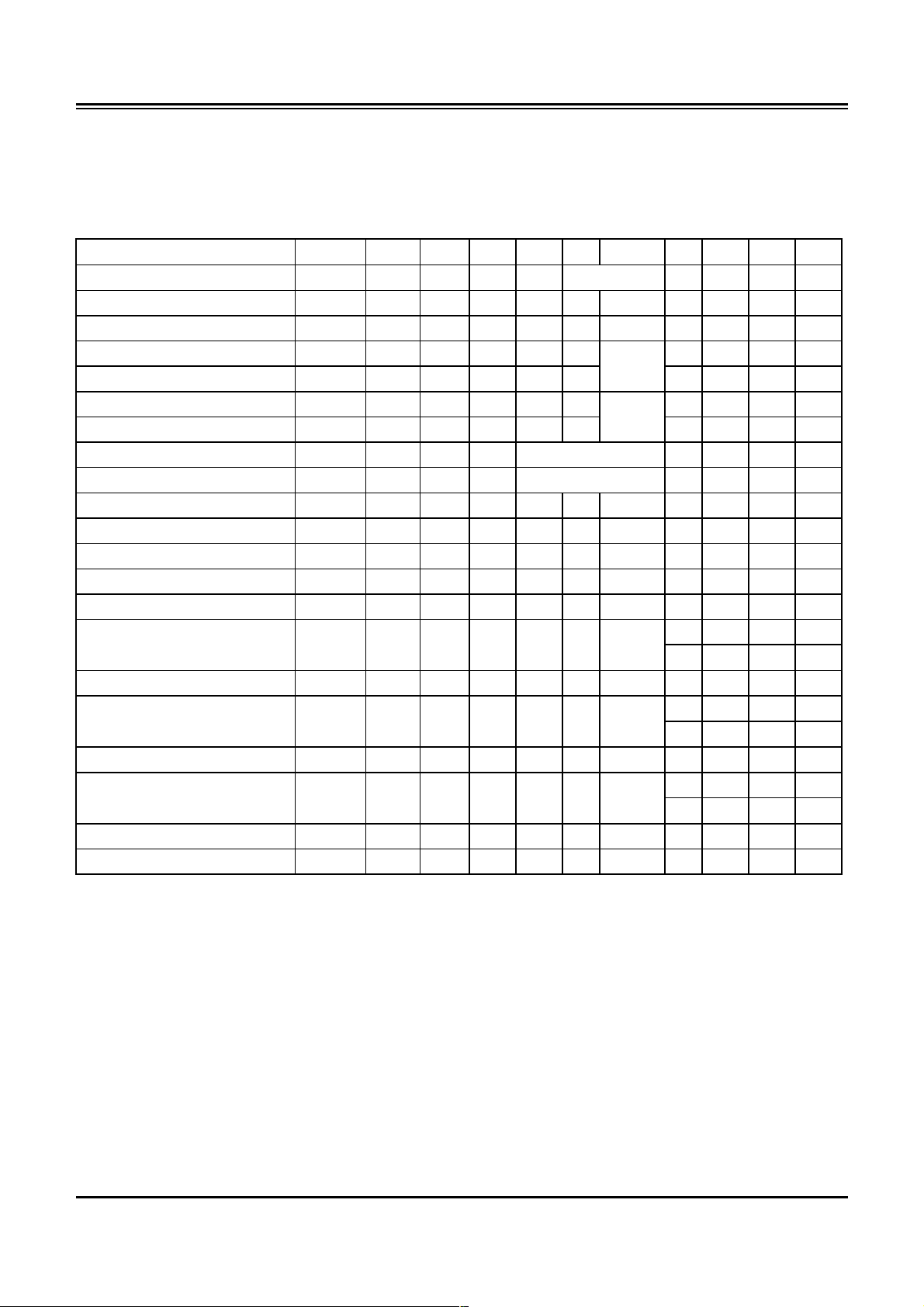
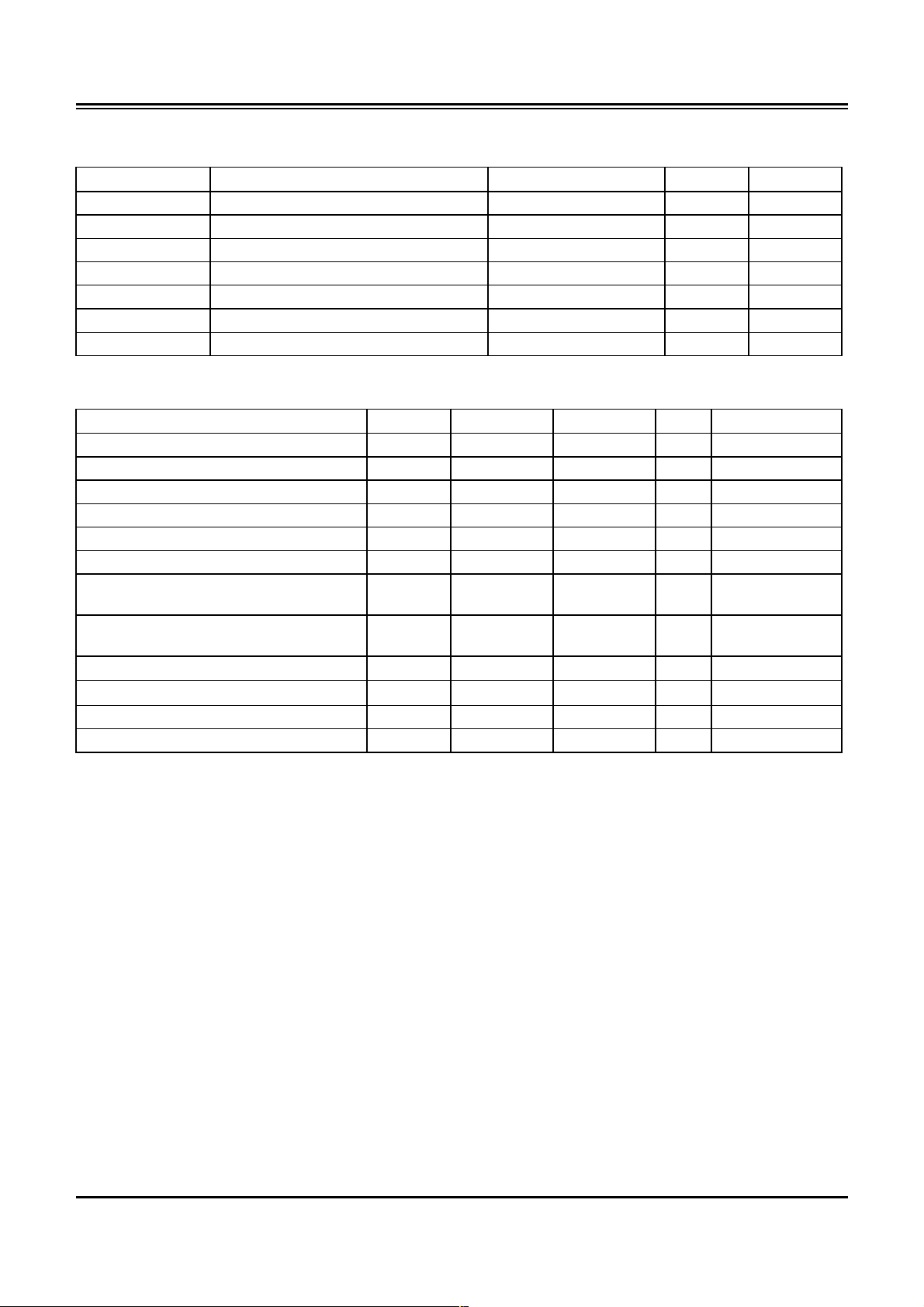
Operation Mode
Fully synchronous operations are performed to latch the com mands at the positive edges of CK. Table 2
shows the truth table for the operation commands.
Table 2. Truth Table (Note (1), (2) )
Command State CKE
BankActivate
BankPrecharge
PrechargeAll
Write
Write and AutoP recharge
Read
Read and Autoprecharge
Mode Register Set
Extended MRS
No-Operation
Burst Stop
Device Deselect
AutoRefresh
SelfRefresh Entry
SelfRefresh Exit
Clock Suspend Mode Entry
Power Down Mode Entry
Clock Suspend Mode Exit
Power Down Mode Exit
Data Write/Out put Enable
Data Mask/Output Disable
Note:
1. V=Valid data, X=Don't Care, L=Low level, H=High level
2. CKE
signal is input level when commands are provided.
n
CKE
signal is input level one clock cycle before the commands are provided.
n-1
3. These are states of bank designated by BS signal.
4. Device state is 1, 2, 4, 8, and full page burst operation.
5. Power Down Mode can not enter in the burst operation.
When this command is asserted in the burst cycle, device state is clock suspend mode.
0,1A10A0-9,11
/CS /RAS /CAS /WE
Idle
(3)
CKEnDM BS
n-1
H X X V Row address L L H H
Any H X X V L X L L H L
Any H X X X H X L L H L
Active
Active
Active
Active
(3)
HXXVL LHLL
(3)
HXXVH
(3)
HXXVL LHLH
(3)
HXXVH
Column
address
(A0 ~ A7)
Column
address
(A0 ~ A7)
LH L L
LH L H
Idle H X X OP code L L L L
Idle H X X OP code L L L L
Any H X X X X X L H H H
(4)
Active
HXXXXXLHHL
Any H XXXX X HXXX
Idle H H X X X X L L L H
Idle H L X X X X L L L H
Idle L HXXX X HXXX
(SelfRefresh)
LH HH
ActiveH LXXX X XXXX
(5)
Any
H LXXX X HXXX
LH H H
ActiveL HXXX X XXXX
Any L HXXX X HXXX
(PowerDown)
LH H H
ActiveHXLXXXXXXX
ActiveHXHXXXXXXX
Etron Confidential 5 Rev. 1.1 Jan. 2002
Page 6
Etr onT ech
Mode Register Set (MRS)
The mode register is divided into various fields depending on functionality.
•
Burst Length Field (A2~A0)
This field specif ies the data length of column access using the A2~A0 pins and selects the
Burst Length to be 2, 4, 8.
A2 A1 A0 Burst Length
0 0 0 Reserved
001 2
010 4
011 8
1 0 0 Reserved
1 0 1 Reserved
1 1 0 Reserved
1 1 1 Reserved
•
Addressing Mode Select Field (A3)
The Addressing Mode can be one of two modes, both Interleave Mode or Sequential Mode.
Both Sequential Mode and Interleave Mode support burst length of 2,4 and 8.
4Mx16 DDR SDRAM
EM658160
A3 Addressing Mode
0 Sequential
1 Interleave
--- Addressing Sequence of Sequential Mode
An internal column address is performed by increasing the address from the column
address which is input to the device. The internal column address is var ied by the Burst
Length as shown in the following table.
Data n 01234567
Column Address
Burst Length 4 words
--- Addressing Sequence of Interleave Mode
A column access is started in the input c olumn address and is performed by inverting the
address bits in the sequence shown in the following table.
Data n Column Address Burst Length
Data 0 A7 A6 A5 A4 A3 A2 A1 A0
Data 1 A7 A6 A5 A4 A3 A2 A1 A0# 4 words
Data 2 A7 A6 A5 A4 A3 A2 A1# A0
Data 3 A7 A6 A5 A4 A3 A2 A1# A0# 8 words
Data 4 A7 A6 A5 A4 A3 A2# A1 A0
Data 5 A7 A6 A5 A4 A3 A2# A1 A0#
Data 6 A7 A6 A5 A4 A3 A2# A1# A0
Data 7 A7 A6 A5 A4 A3 A2# A1# A0#
n n+1 n+2 n+3 n+4 n+5 n+6 n+7
2 words
8 words
Full Page (Even starting address)
Etron Confidential 6 Rev. 1.1 Jan. 2002
Page 7
Etr onT ech
•
CAS Latency Field (A6~A4)
This field specifies the num ber of clock cycles from the asser tion of the Read com m and to the
first read data. The m inimum whole value of CAS Latency depends on the frequency of CK.
The minimum whole value satisfying the following formula must be programmed into this field.
(min) ≤ CAS Latency X t
t
CAC
A6 A5 A4 CAS Latency
0 0 0 Reserved
010 2 clocks
011 3 clocks
1 0 1 Reserved
1 1 0 2.5 clocks
1 1 1 Reserved (3.5 clocks)
•
Test Mode field (A8~A7)
These two bits are used to enter the test mode and m ust be programmed to "00" in norm al
operation.
A8 A7 Test Mode
0 0 Normal mode
1 0 DLL Reset
X 1 Test mode
•
( BS0, BS1)
4Mx16 DDR SDRAM
CK
EM658160
BS1 BS0 An ~ A0
RFU 0 MRS Cycle
RFU 1 Extended Functions (EMRS)
Extended Mode Register Set (EMRS)
BS1 BS0 A11~ A1 A0
RFU 1 RFU 0 DLL Enable
RFU 1 RFU 1 DLL Disable
Etron Confidential 7 Rev. 1.1 Jan. 2002
Page 8
Etr onT ech
4Mx16 DDR SDRAM
EM658160
Absolute Maximum Rating
Symbol Item Rating Unit Note
VIN, V
VDD, V
T
OPR
T
STG
T
SOLDER
P
I
OUT
OUT
DDQ
D
Input, Output Voltage - 0.3~ VDD + 0.3 V 1
Power Supply Voltage - 0.3~3.6 V 1
Operating Temperature 0~70 °C 1
Storage Temperature - 55~150 °C 1
Soldering Temperature (10s) 260 °C 1
Power Dissipation 1 W 1
Short Circuit Output Current 50 mA 1
Recommended D.C. Operating Conditions (Ta = 0 ~ 70
Parameter Symbol Min. Max. Unit Note
Power Supply Voltage V
Power Supply Voltage (for I/O Buffer) V
Input Reference Voltage V
Termination Voltage V
Input High Voltage (DC) V
Input Low Voltage (DC) V
Input Voltage Level, CLK and CLK#
IH
IL
V
IN
inputs
Input Different Voltage, CLK and CLK#
V
ID
inputs
Input leakage current I
Output leakage current I
Output High Voltage V
Output Low Voltage V
DD
DDQ
REF
TT
(DC) V
(DC) -0.3 V
(DC) -0.3 V
(DC) -0.36 V
I
OZ
OH
OL
3.0 3.6 V
2.3 2.7 V
1.15 1.35 V
V
- 0.04 V
REF
+ 0.18 V
REF
REF
DDQ
REF
DDQ
DDQ +
-5 5
-5 5
VTT + 0.76 - V I
VTT – 0.76 V I
°C)
+ 0.04 V
+ 0.3 V
– 0.18 V
+ 0.3 V
0.6 V
µ
µ
A
A
= -15.2 mA
OH
= +15.2 mA
OL
Etron Confidential 8 Rev. 1.1 Jan. 2002
Page 9

Etr onT ech
4Mx16 DDR SDRAM
EM658160
Capacitance (VDD = 3.3V, f = 1MHz, Ta = 25 °C)
Symbol Parameter Min. Max. Unit
C
IN
Input Capacitance (except for CK pin) 2.5 5 pF
Input Capacitance (CK pin) 2.5 4 pF
C
I/O
DQ, DQS, DM Capacitance 4 6.5 pF
Note: These parameters are periodically sampled and are not 100% tested.
Recommended D.C. Operating Conditions (VDD = 3.3V ± 0.3, Ta = 0~70 °C)
Max.
Parameter Symbol
Operation Current
(one bank active)
Operation Current
(one bank active)
Precharge Powerdown Standby Current
Idel Standby Current
Active Power-down
Standby Current
Active Standby
Current
Operation Current
(Read)
Operation Current
(Write)
Auto Refresh Current
I
DD0
I
DD1
I
DD2P
I
DD2N
I
DD3P
I
DD3N
I
DD4R
I
DD4W
I
DD5
t
= min, tCK = min
RC
Active-precharge
Burst = 2, t
= 0mA, Active-Read-Precharge
I
OUT
CKE ≤ VIL(max), t
= min, CL = 3
RC
CK
= min,
All banks idle
CKE ≥ VIH(min), CS# ≥ VIH(min),
= min
t
CK
All banks ACT, CKE ≤ VIL(max),
= min
t
CK
One bank; Active-Precharge,
= t
t
RC
max), tCK = min
RAS(
Burst = 2, CL = 3, tCK = min,
= 0mA
I
OUT
Burst = 2, CL = 3, tCK = min
t
min)
RC(
250/240/230/220/190/180/160
320/300/260/250/220/210/200
180/170/160/155/145/140/135
330/310/270/250/220/200/180
330/310/270/250/220/200/180
190/180/170/155/145/140/135
- 3.3/3.5/4/5/6/7/8
80/80/80/65/65/60/55
170/160/150/130/110/100/90
80/80/80/65/65/60/55
UNIT
mA
Self Refresh Current
I
DD6
CKE ≤ 0.2v
2
Etron Confidential 9 Rev. 1.1 Jan. 2002
Page 10

Etr onT ech
4Mx16 DDR SDRAM
EM658160
Electrical Characteristics and Recommended A.C. Operating Conditions
(VDD = 3.3 ± 0.3 V, Ta = 0~70 °C)
- 3.3/3.5/4/5/6/7/8
Symbol Parameter
t
RC
t
RFC
t
RAS
t
RCD
t
RP
t
RRD
tw
t
CDLR
t
CCD
t
CK
t
CH
t
CL
t
DQSCK
t
AC
t
DQSQ
t
RPRE
t
RPST
t
DQSS
t
WPRES
t
WPREH
t
WPST
t
DQSH
t
DQSL
t
IS
t
IH
t
MRD
t
DS
t
DH
t
QH
t
PDEX
t
XSA
Row cycle time
Refresh row cycle time
Row active time
/RAS to /CAS Delay
Row precharge time
Row active to Row active delay
Write recovery time
R
Last data in to Read command
Col. Address to Col. Address delay
Clock cycle time
Clock high level width
Clock low level width
DQS-out access time from CK,/CK
Output access time from CK,/CK
DQS-DQ Skew
Read preamble
Read postamble
CK to valid DQS-in
DQS-in setup time
DQS-in hold time
DQS write postamble
DQS in high level pulse width
DQS in low level pulse width
Address and Control input setup time
Address and Control input hold time
Mode register set cycle time
DQ & DM setup time to DQS
DQ & DM hold time to DQS
Output DQS valid window
Power down exit time
Self refresh exit to active
command delay
t
XSR
Self refresh exit to read
command delay
44/44/44/55/60/70/80 ns
56/56/56/70/84/91/96
32/32/32/40/42/49/56 120000 ns
12/12/12/15/18/21/24 ns
12/12/12/15/18/21/24 ns
6.6/7/8/10/12/14/16 ns
CL*=3 3.3/3.5/4/5/6/7/8 15
CL*=2.5 5/5/5.5/6/7.5/8/9 15
CL*=2 6/6/7/8/9/10/11 15
-0.6/-0.6/-0.6/-0.7/-0.7/-0.75/-0.8 0.6/0.6/0.6/0.7/0.7/0.75/0.8
-0.6/-0.6/-0.6/-0.7/-0.7/-0.75/-0.8 0.6/0.6/0.6/0.7/0.7/0.75/0.8
-0.5/-0.5/-0.5/-0.5/-0.5/-0.5/-0.6 0.5/0.5/0.5/0.5/0.5/0.5/0.6
0.4/0.4/0.4/0.4/0.45/0.5/0.55 ns
0.4/0.4/0.4/0.4/0.45/0.5/0.55 ns
0.4/0.4/0.4/0.4/0.45/0.5/0.55
0.4/0.4/0.4/0.4/0.45/0.5/0.55
12/12/11/11/10/10/10
Min. Max. Unit
2t
2.5t
CK-tDQSS
t
1t
0.45 0.55
0.45 0.55
0.9 1.1 t
0.4 0.6 t
0.75 1.25 t
0.4 0.6 t
0.4 0.6 t
0.4 0.6 t
1.1
1.1
1t
0.3 t
+1t
t
IS
CK
tIS+2t
CK
200
ns
ns
t
t
ns
ns
ns
ns
ns
ns
ns
ns
t
t
CK
CK
CK
CK
CK
CK
CK
CK
CK
CK
CK
CK
CK
CK
CK
Etron Confidential 10 Rev. 1.1 Jan. 2002
Page 11

Etr onT ech
Note:
1. Stress greater than those listed under "Absolute Maxim um Ratings" may cause permanent dam age to the
device.
4Mx16 DDR SDRAM
EM658160
2. All voltages are referenced to V
3. These parameters depend on the cycle rate and these values are measured by the cycle rate under the
minimum value of t
4. Power-up sequence is described in Note 6.
5. A.C. Test Conditions
and tRC. Input signals are changed one time during tCK.
CK
SS
.
SSTL_2 Interface
Reference Level of Output Signals (V
Output Load Reference to the Under Output Load (A)
Input Signal Levels V
Input Signals Slew Rate 1 V/ns
Reference Level of Input Signals 0.5 * V
) 0.5 * V
RFE
Ω
25
Output
+0.35 V / V
REF
0.5*V
DDQ
25
DDQ
REF
DDQ
Ω
-0.35 V
30pF
SSTL_2 A.C. Test Load
Power up Sequence
6.
Power up must be performed in the following sequence.
1) Power must be applied to V
maintain CKE “LOW”. Power applied to V
2) After power-up, No-Operation of 200 µ−seconds minimum is required.
3) Start clock and keep CKE “HIGH” to maintain either No-Operation or Device Deselect at the input.
4) Issue EMRS – enable DLL.
5) Issue MRS – reset DLL and set device to idle with bit A8 (An additional 200 cycles min of clock are
needed for DLL lock)
6) Precharge all banks of the device.
7) Two or more Auto Refresh commands.
8) Issue MRS – Initialize device operation.
and V
DD
(simultaneously) when all input signals are held "NOP" state and
DDQ
the same time as V
DDQ
TT
and V
REF.
Etron Confidential 11 Rev. 1.1 Jan. 2002
Page 12

Etr onT ech
Timing Waveforms
4Mx16 DDR SDRAM
EM658160
Figure 1. AC Parameters for Read Timing
CL
CK
/CK
CMD
ADDR
/CS
t
CH
t
IS
t
IH
t
Read
IS
t
IH
t
CK
t
DQSQ
t
RPRE
t
(Burst Length=4, CAS Latency=2.5)
RPST
t
DQS
DQ
Preamble
Postamble
AC
t
D1 D2
D0
D3
Etron Confidential 12 Rev. 1.1 Jan. 2002
Page 13

Etr onT ech
4Mx16 DDR SDRAM
EM658160
Figure 2. AC Parameters for Write Timing
CK
/CK
CMD
ADDR
/CS
DQ
Write
D0
D1
(Burst Length=4)
D2
D3
DQS
WPRES
t
Preamble
DQSS
t
DH
t
DS
t
t
DSL
DSH
t
WPST
t
Postamble
Etron Confidential 13 Rev. 1.1 Jan. 2002
Page 14

Etr onT ech
4Mx16 DDR SDRAM
EM658160
Figure 3. Read Command to Output Data Latency
CK
/CK
CMD
CL=2
DQ
DQS
CL=2.5
DQ
DQS
Read
Preamble
DA0
DA1
Postamble
DA0
DA1
Postamble
(Burst Length=2)
CL=3
DQ
DQS
Preamble
Preamble
DA0
DA1
Postamble
Etron Confidential 14 Rev. 1.1 Jan. 2002
Page 15

Etr onT ech
4Mx16 DDR SDRAM
EM658160
Figure 4. Read Followed by Write
CK
/CK
RRD
t
RCDR
t
Activate
Read
CMD
ADDR
Row/Bank0 Col/Bank0
/CS
DQ
DQS
ACT
Rol/Bank1
Preamble
(Burst Lenth=4, CAS Latency=3)
Write
Col/Bank0
D3
D2D1
D0
Postamble
Etron Confidential 15 Rev. 1.1 Jan. 2002
Page 16

Etr onT ech
4Mx16 DDR SDRAM
EM658160
Figure 5. Write followed by Read
CK
/CK
WTR
t
CMD
ADDR
/CS
DQ
Write
Col
Read
Col
D0 D1 D3D2
(Burst Lenth=4, CAS Latency=3)
D0 D1
D2
D3
DQS
Etron Confidential 16 Rev. 1.1 Jan. 2002
Page 17

Etr onT ech
4Mx16 DDR SDRAM
EM658160
Figure 6. Precharge Termination of a Burst Read
CK
/CK
Precharge
CMD
ADDR
/CS
DQ
DQS
Read
Col
Bank Bank
RP
t
Preamble
(Burst Length=4, CAS Latency=3)
ACT
D1
D0
Postamble
Etron Confidential 17 Rev. 1.1 Jan. 2002
Page 18

Etr onT ech
4Mx16 DDR SDRAM
EM658160
Figure 7. Precharge Termination of a Burst Write
CK
/CK
RC
t
Activate
CMD
ADDR
Row/Bank Col/Bank
/CS
DQM
RCD
t
Write
t
RAS
Precharge Activate
Row/Bank Row/Bank
RP
QDH
t
t
WR
t
DS
t
(Burst Length=4)
DQ
DQS
Preamble
D0
D1
masked by DQM
Postamble
Etron Confidential 18 Rev. 1.1 Jan. 2002
Page 19

Etr onT ech
4Mx16 DDR SDRAM
EM658160
Figure 8. Auto Precharge after Read Burst
CK
/CK
RP
t
ReadA
ReadA
Auto Precharge
Auto Precharge
ACT
D0
RP
t
D0 D1
D1
ACT
D3D2
BL=2
CMD
DQ
BL=4
CMD
DQ
(CAS Latency=3)
BL=8
CMD
DQ
ReadA
RP
t
Auto Precharge
D0 D1 D3D2 D4 D5 D7D6
ACT
Etron Confidential 19 Rev. 1.1 Jan. 2002
Page 20

Etr onT ech
4Mx16 DDR SDRAM
Figure 9. Auto Precharge after Write Burst
CK
/CK
EM658160
BL=2
CMD
DQ
DQS
BL=4
CMD
DQ
DQS
BL=8
CMD
DQ
WriteA
Preamble
WriteA
Preamble
WriteA
Auto Precharge
WR
t
D0
D1
Postamble
RP
t
Auto Precharge
WR
t
D0 D1
D0 D1 D3D2 D4 D5 D7D6
D3D2
Postamble
ACT
ACT
RP
t
Auto Precharge
WR
t
RP
t
ACT
Preamble
DQS
Postamble
Etron Confidential 20 Rev. 1.1 Jan. 2002
Page 21

Etr onT ech
4Mx16 DDR SDRAM
EM658160
Figure 10. Read Terminated By Burst Stop
CK
/CK
CMD
ADDR
/CS
CL=3
DQ
Read
Col
BST
(Burst Length=8)
D1
D0
D2
D3
DQS
Etron Confidential 21 Rev. 1.1 Jan. 2002
Page 22

Etr onT ech
4Mx16 DDR SDRAM
EM658160
Figure 11. Read Terminated by Read
CK
/CK
CCD
t
CMD
ADDR
/CS
DQ
DQS
Read
Col A
Read
Col B
(Burst Length=4, CAS Latency=3)
DA1
DA0
DB0
DB3DB2DB1
Etron Confidential 22 Rev. 1.1 Jan. 2002
Page 23

Etr onT ech
4Mx16 DDR SDRAM
Figure 12. Mode Register Set Command
CK
/CK
RP
t
EM658160
1 clk
CMD
ADDR
/CS
MRS ACT
Precharge
Row
MRS Data
Etron Confidential 23 Rev. 1.1 Jan. 2002
Page 24

Etr onT ech
4Mx16 DDR SDRAM
Figure 13. Active / Precharge Power Down Mode
CK
/CK
PDEX
IS
t
CKE
CMD
Note: 1. All banks should be in idle state prior to entering precharge power down mode.
Activate /
Precharge
Note 1,2
t
Any
Command
EM658160
2. One of the banks should be in active state prior to entering active power down mode.
Etron Confidential 24 Rev. 1.1 Jan. 2002
Page 25

Etr onT ech
4Mx16 DDR SDRAM
Figure 14. Self Refresh Entry and Exit Cycle
CK
/CK
Self Refresh Enter
CMD
CKE
Auto
Refresh
IS
t
Self Refresh Exit
NOP
RC
t
EM658160
t
is required before any command can be applied,
RC
and 200 cycles of clk are required before a READ
command can be applied.
Etron Confidential 25 Rev. 1.1 Jan. 2002
Page 26

Etr onT ech
4Mx16 DDR SDRAM
66 Pin TSOP II Package Outline Drawing Information
Units: mm
22 .22 0.13
66
34
EM658160
+ 0.085
0.125
- 0.005
0.8 TYP
1
0.71 TYP
1. 00 0. 10
0.05 MIN
11.76 0.20
0. 5 0.1
1.20 MAX
0 ~ 8
0.10 MAX
0.25 TYP
10.16 0.13
33
0 . 30 0. 080.65 TYP
Etron Confidential 26 Rev. 1.1 Jan. 2002
 Loading...