

Page 1

GENERAL DESCRIPTION
EM73963A is an advanced single chip CMOS 4-bit micro-controller. It contains 16K-byte ROM, 372-nibble
RAM, 4-bit ALU, 13-level subroutine nesting, 22-stage time base, two 12-bit timer/counters for the kernel
function. EM73963A also equipped with 5 interrupt sources, 3 I/O ports (including 1 input port and 2 bidirection
ports), LCD display (40x8), built-in sound generator.
It's low power consumption and high speedfeature are further strengten with DUAL, SLOW, IDLE and STOP
operation mode for optimized power saving.
FEATURES
Operation voltage : 2.4V to 5.5V.
Clock source : Dual clock system. Low-frequency oscillator is Crystal or RC oscillator (32KHz,
Oscillation frequency : 480K, 1M, 2M and 4M Hz are both available for high frequency clock by mask option.
Instruction set : 107 powerful instructions.
Instruction cycle time : Up to 2 µs for 4 MHz (high speed clock).
ROM capacity : 16K X 8 bits.
RAM capacity : 372 X 4 bits.
Input port : 1 port (P0.0-P0.3), IDLE/STOP releasing function is available by mask option.(each
Bidirection port : 2 ports (P4, P8). P4.0 and SOUND are available by mask option. IDLE/STOP release
12-bit timer/counter : Two 12-bit timer/counters are programmable for timer, event counter and pulse width
Built-in time base counter : 22 stages.
Subroutine nesting : Up to 13 levels.
Interrupt : External . . . . . 2 input interrupt sources.
LCD driver : 40 X 8 dots, 1/8 duty, 1/5 bias.
Sound effect : Tone generator, random generator and volume control.
Power saving function :SLOW, IDLE, STOP operation modes.
Package type : Chip form 69 pins.
EM73963A
4-BIT MICRO-CONTROLLER FOR LCD PRODUCT
connect a external resistor) by mask option and high-frequency oscillator is RC
oscillator (connect a external resistor and a capacitor).
External clock and internal clock is available by mask option.
244 µs for 32768 Hz (low speed clock).
input pin has a pull-up and pull-down resistor available by mask option).
function for P8(0..3) is available by mask option.
measurement mode.
Internal . . . . . . 2 Timer overflow interrupts.
1 Time base interrupt.
* This specification are subject to be changed without notice.
6.14.2001
1
Page 2
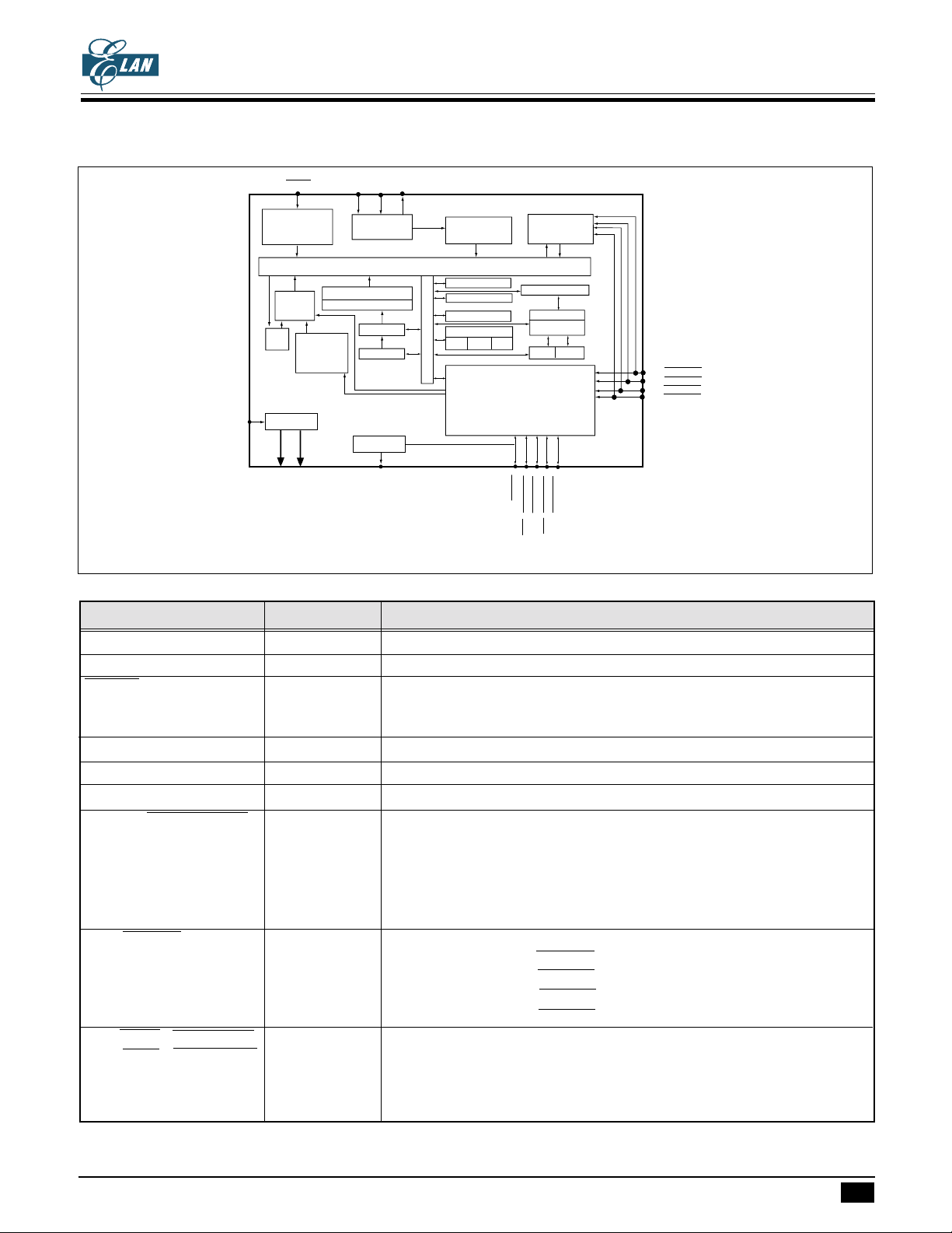
FUNCTION BLOCK DIAGRAM
RESET
CLK
LXIN
EM73963A
4-BIT MICRO-CONTROLLER FOR LCD PRODUCT
LXOUT
V1~V4
Reset
Control
Interrupt
Control
Time
Base
LCD Driver
COM0~COM7
Timer/Counter
(TA,TB)
SEG0~SEG39
Clock
Generator
Instruction Decoder
Instruction Register
ROM
PC
SOUND GEN.
SOUND
System Control
Data Bus
Timing
Generator
Data pointer
ACC
ALU
Flag
ZCS
I/O Control
Clock Mode
Control
Stack pointer
Stack
RAM
HR
LR
P4.0/SOUND
P8.2(INT0)/WAKEUPC
P8.0(INT1)/WAKEUPA
P8.1(TRGB)/WAKEUPB
P8.3(TRGA)/WAKEUPD
P0.0/WAKEUP0
P0.1/WAKEUP1
P0.2/WAKEUP2
P0.3/WAKEUP3
PIN DESCRIPTIONS
Symbol Pin-type Function
V
DD
V
SS
RESET RESET-A System reset input signal, low active
CLK OSC-C RC or external clock source connecting pin for high speed clock source.
LXIN OSC-B/OSC-F Crystal/RC connecting pin for low speed clock source.
LXOUT OSC-B/OSC-F Crystal/RC connecting pin for low speed clock source.
P0(0..3)/WAKEUP0..3 INPUT-B 4-bit input port with IDLE/STOP releasing function
P4.0/SOUND I/O-O 1-bit bidirection I/O port or inverse sound effect output
P8.0(INT1)/WAKEUPA I/O-L 2-bit bidirection I/O port with external interrupt sources input and IDLE
P8.2(INT0)/WAKEUPC /STOP releasing function
Power supply (+)
Power supply (-)
mask option : none
pull-up
mask option : wakeup enable, pull-up
wakeup enable, none
wakeup disable, pull-up
wakeup disable, pull-down
wakeup disable, none
mask option : SOUND enable, push-pull, high current PMOS
SOUND disable, open-drain
SOUND disable, push-pull, high current PMOS
SOUND disable, push-pull, low current PMOS
mask option : wakeup enable, push-pull
wakeup disable, push-pull
wakeup disable, open-drain
* This specification are subject to be changed without notice.
6.14.2001
2
Page 3
EM73963A
4-BIT MICRO-CONTROLLER FOR LCD PRODUCT
Symbol Pin-type Function
P8.1(TRGB)/WAKEUPB I/O-L 2-bit bidirection I/O port with time/counter A,B external input and IDLE
P8.3(TRGA)/WAKEUPD /STOP releasing function
mask option : wakeup enable, push-pull
wakeup disable, push-pull
wakeup disable, open-drain
SOUND Built-in sound effect output
V1, V2, V3, V4 LCD bias voltage input
COM0~COM7 LCD common output pins
SEG0~SEG39 LCD segment output pins
TEST Tie VSS as package type, no connecting as COB type
FUNCTION DESCRIPTIONS
PROGRAM ROM ( 16K X 8 bits )
16 K x 8 bits program ROM contains user's program and some fixed data.
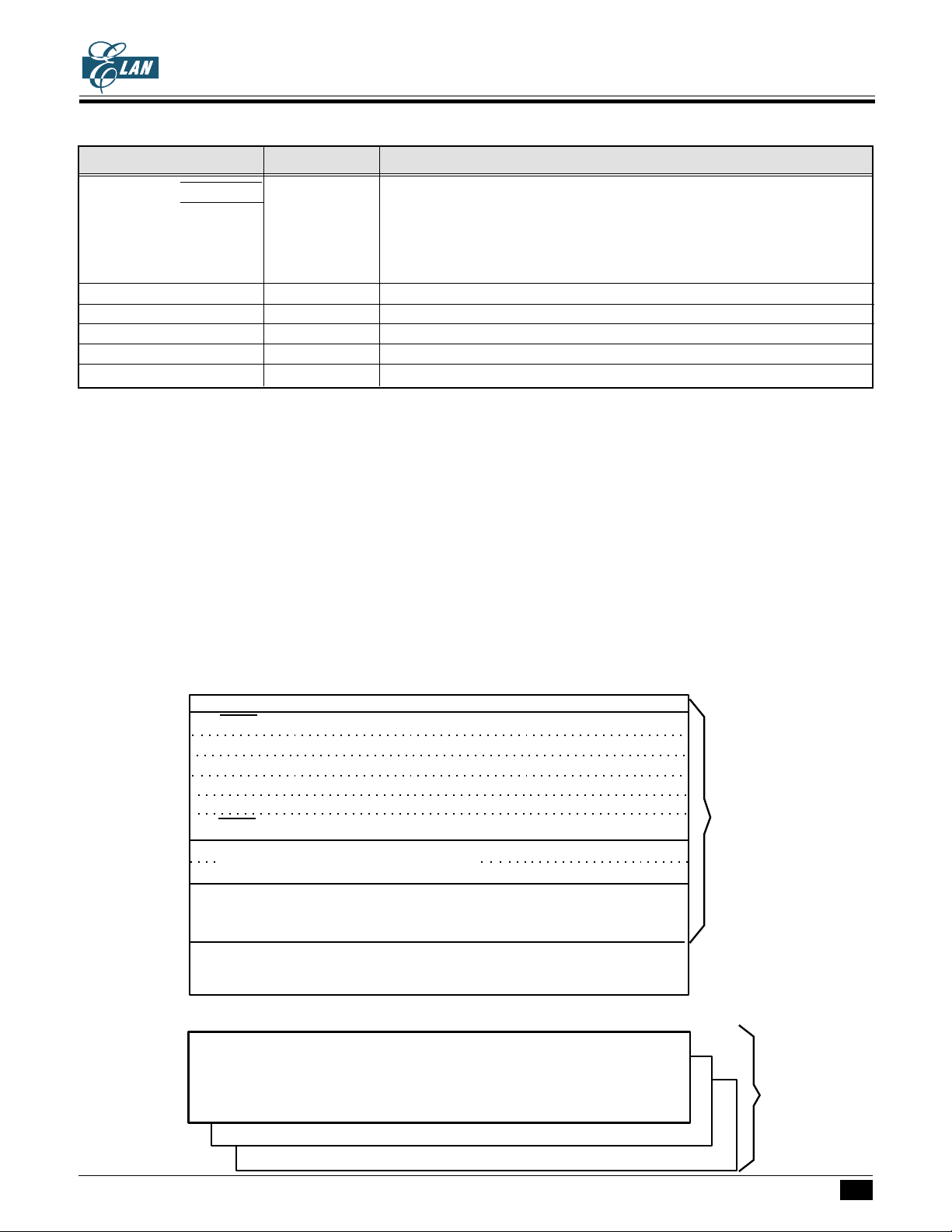
The basic structure of the program ROM may be categorized into 5 partitions.
1. Address 0000h: Reset start address.
2. Address 0002h - 000Ch : 5 kinds of interrupt service routine entry addresses.
3. Address 000Eh-0086h : SCALL subroutine entry address, only available at 000Eh,0016h,001Eh,0026h, 002Eh,
0036h, 003Eh, 0046h, 004Eh, 0056h, 005Eh, 0066h, 006Eh, 0076h, 007Eh,0086h.
4. Address 0000h - 07FFh : LCALL subroutine entry address.
5. Address 0000h - 1FFFh : Except used as above function, the other region can be used as user's program and
data region.
address Bank 0 :
0000h Reset start address
0002h INT0; interrupt service routine entry address
0004h Reserved
0006h TRGA
0008h TRGB
000Ah TBI
000Ch INT1
000Eh
0086h
.
.
.
.
.
.
SCALL, subroutine call entry address
07FFh
0800h
Subroutine call entry address
designated by [LCALL a]
instruction
0FFFh
1000h
Bank 1
1FFFh
Bank 2
Bank 3
* This specification are subject to be changed without notice.
Data table for
[LDAX],[LDAXI]
instruction
6.14.2001
3
Page 4
EM73963A
4-BIT MICRO-CONTROLLER FOR LCD PRODUCT
User's program and fixed data are stored in the program ROM. User's program is executed using the PC value
to fetch an instruction code.
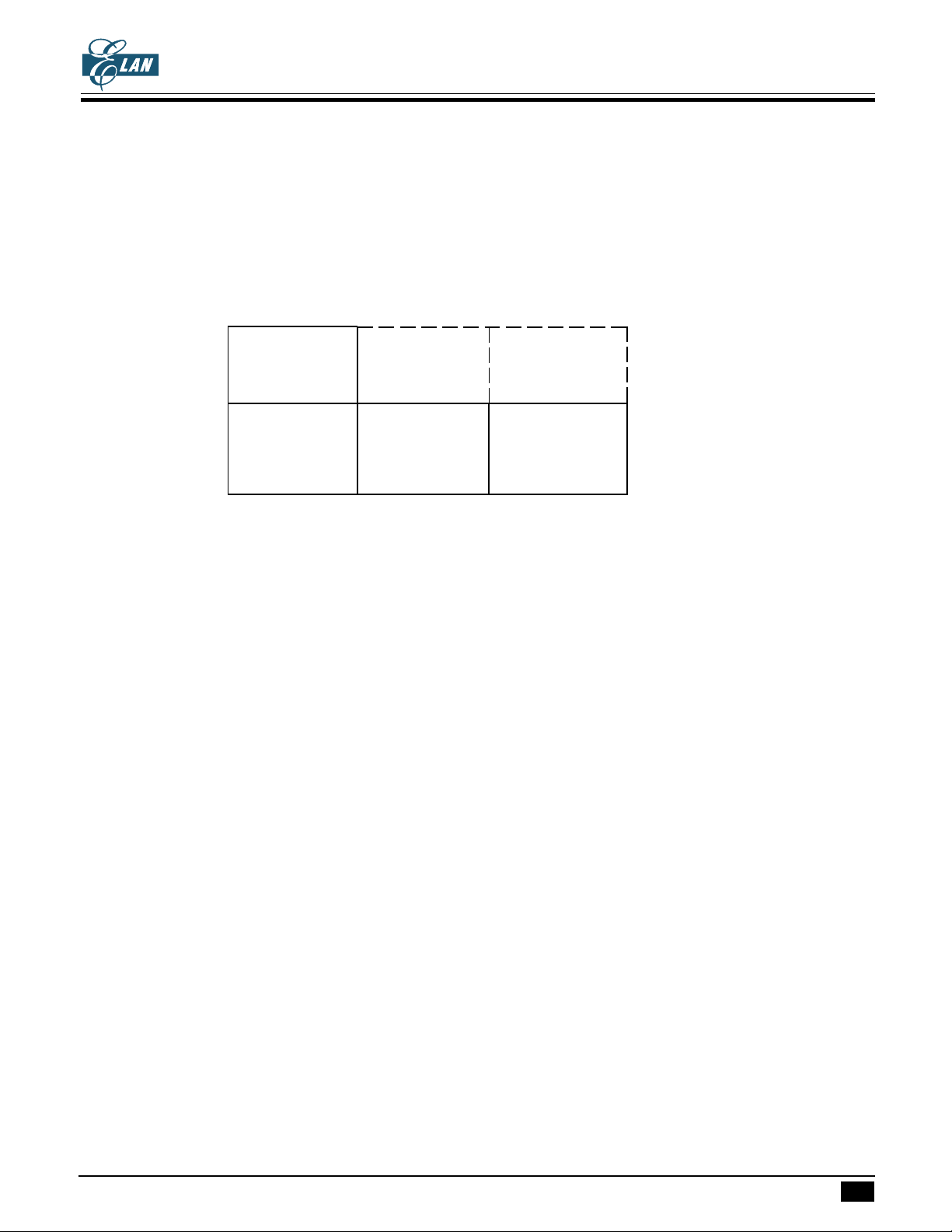
The 16Kx8 bits program ROM can be divided into 4 banks. There are 4Kx8 bits per bank.
The program ROM bank is selected by P3(1..0). The program counter is a 13-bit binary counter. The PC
and P3 are initialized to "0" during reset.
When P3(1..0)=00B, the bank0 and bank1 of program ROM will be selected. P3(1..0)=01B, the bank0 and
bank2 will be selected.
Address P3=xx00B P3=xx01B P3=xx10B
0000h
:
: Bank0 Bank0 Bank0
0FFFh
1000h
:
: Bank1 Bank2 Bank3
1FFFh
PROGRAM EXAMPLE:
BANK 0
START: :
:
:
LDIA #00H ; set program ROM to bank1
OUTA P3
B XA1
:
XA : :
:
LDIA #01H ; set program ROM to bank2
OUTA P3
B XB1
:
XB : :
:
LDIA #02H ; set program ROM to bank3
OUTA P3
B XC1
:
XC : :
:
BXD
XD : :
:
:
; - - - - - - - - - - - - - - - - - - - - - - - - - - - - - - - - - - - - - - - - - - - - - - - - - - - - - - - - - - - - - - - - - - - - - - - - - - - - -
BANK 1
XA1 : :
:
BXA
:
XA2 : :
* This specification are subject to be changed without notice.
6.14.2001
4
Page 5

EM73963A
4-BIT MICRO-CONTROLLER FOR LCD PRODUCT
B XA2
:
; - - - - - - - - - - - - - - - - - - - - - - - - - - - - - - - - - - - - - - - - - - - - - - - - - - - - - - - - - - - - - - - - - - - - - - - - - - - - -
BANK 2
XB1 : :
:
BXB
:
XB2 : :
B XB2
:
; - - - - - - - - - - - - - - - - - - - - - - - - - - - - - - - - - - - - - - - - - - - - - - - - - - - - - - - - - - - - - - - - - - - - - - - - - - - - -
BANK 3
XC1 : :
:
BXC
:
XC2 : :
B XC2
Fixed data can be read out by table-look-up instruction. Table-look-up instruction requires the Data point
(DP) to indicate the ROM address in obtaining the ROM code data (Except bank 0) :
LDAX Acc
LDAXI Acc
←←
← ROM[DP]
←←
←←
← ROM[DP]
←←
L
,DP+1
H
DP is a 12-bit data register that stores the program ROM address as pointer for the ROM code data.
User has to initially load ROM address into DP with instructions "STADPL", and "STADPM, STADPH",
then to obtain the lower nibble of ROM code data by instruction "LDAX" and higher nibble by instruction
"LDAXI"
PROGRAM EXAMPLE: Read out the ROM code of address 1777h by table-look-up instruction.
LDIA #07h;
STADPL ; [DP]
STADPM ; [DP]
STADPH ; [DP]
:
OUT #00H , P3 ; Set in bank 1
LDL #00h;
LDH #03h;
LDAX ; ACC ← 6h
STAMI ; RAM[30] ← 6h
LDAXI ; ACC ← 5h
STAM ; RAM[31] ← 5h
;
ORG 1777h
DATA 56h;
← 07h
L
← 07h
M
← 07h, Load DP=777h
H
DATA RAM (372-nibble )
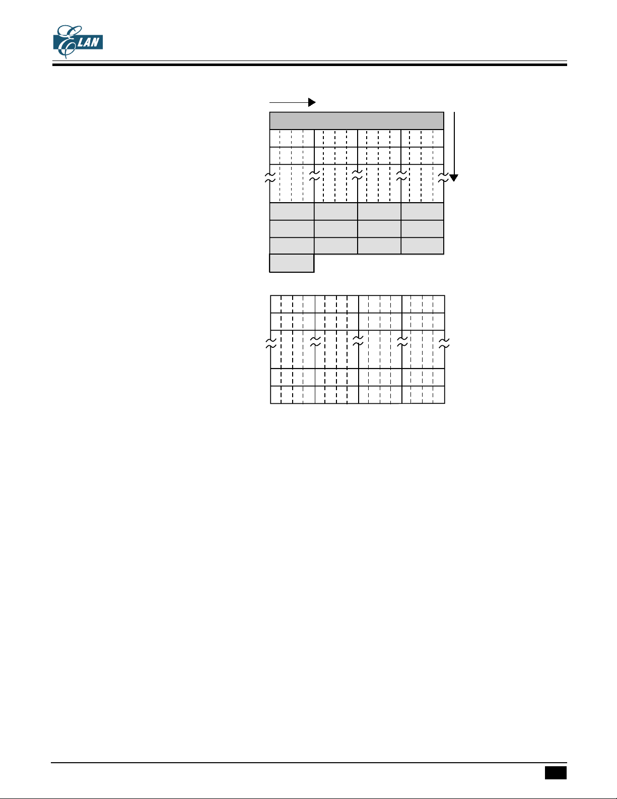
A total 372 - nibble data RAM is available from address 000 to 17Fh
Data RAM includes the zero page region, stacks and data area.
* This specification are subject to be changed without notice.
6.14.2001
5
Page 6
EM73963A
4-BIT MICRO-CONTROLLER FOR LCD PRODUCT
Bank 0
Bank 1
Address
000h - 00Fh
010h - 01Fh
020h - 02Fh
:
:
:
0C0h - 0CFh
0D0h - 0DFh
0E0h - 0EFh
0F0h - 0F3h
100h - 10Fh
110h - 11Fh
:
:
:
160h - 16Fh
Increment
Level 0
Level 4
Level 8
Level 12
Zero-page
Level 1
Level 5
Level 9
Level 2
Level 6
Level 10
Increment
Level 3
Level 7
Level 11
170h - 17Fh
ZERO- PAGE:
From 000h to 00Fh is the zero-page location. It is used as the zero-page address mode pointer for the
instruction of "STD #k,y; ADD #k,y; CLR y,b; CMP k,y".
PROGRAM EXAMPLE: To wirte immediate data "07h" to RAM [03] and to clear bit 2 of RAM [0Eh].
STD #07h, 03h ; RAM[03] ← 07h
CLR 0Eh,2 ; RAM[0Eh]
← 0
2
STACK:
There are 13 - level (maximum) stack levels that user can use for subroutine (including interrupt and CALL).
User can assign any level be the starting stack by providing the level number to stack pointer (SP).
When an instruction (CALL or interrupt) is invoked, before enter the subroutine, the previous PC address is
saved into the stack. Until returned from those subroutines, the PC value is restored by the data saved in stack.
DATA AREA:
Except the area used by user's application, the whole RAM can be used as data area for storing and loading
general data.
ADDRESSING MODE
The 372 nibble data memory consists of two banks (bank 0 and bank 1). There are 244x4 bits (address
000h~0F3h) in bank 0 and 128x4 bits (address 100h~17Fh) in bank 1.
* This specification are subject to be changed without notice.
6.14.2001
6
Page 7
EM73963A
R
4-BIT MICRO-CONTROLLER FOR LCD PRODUCT
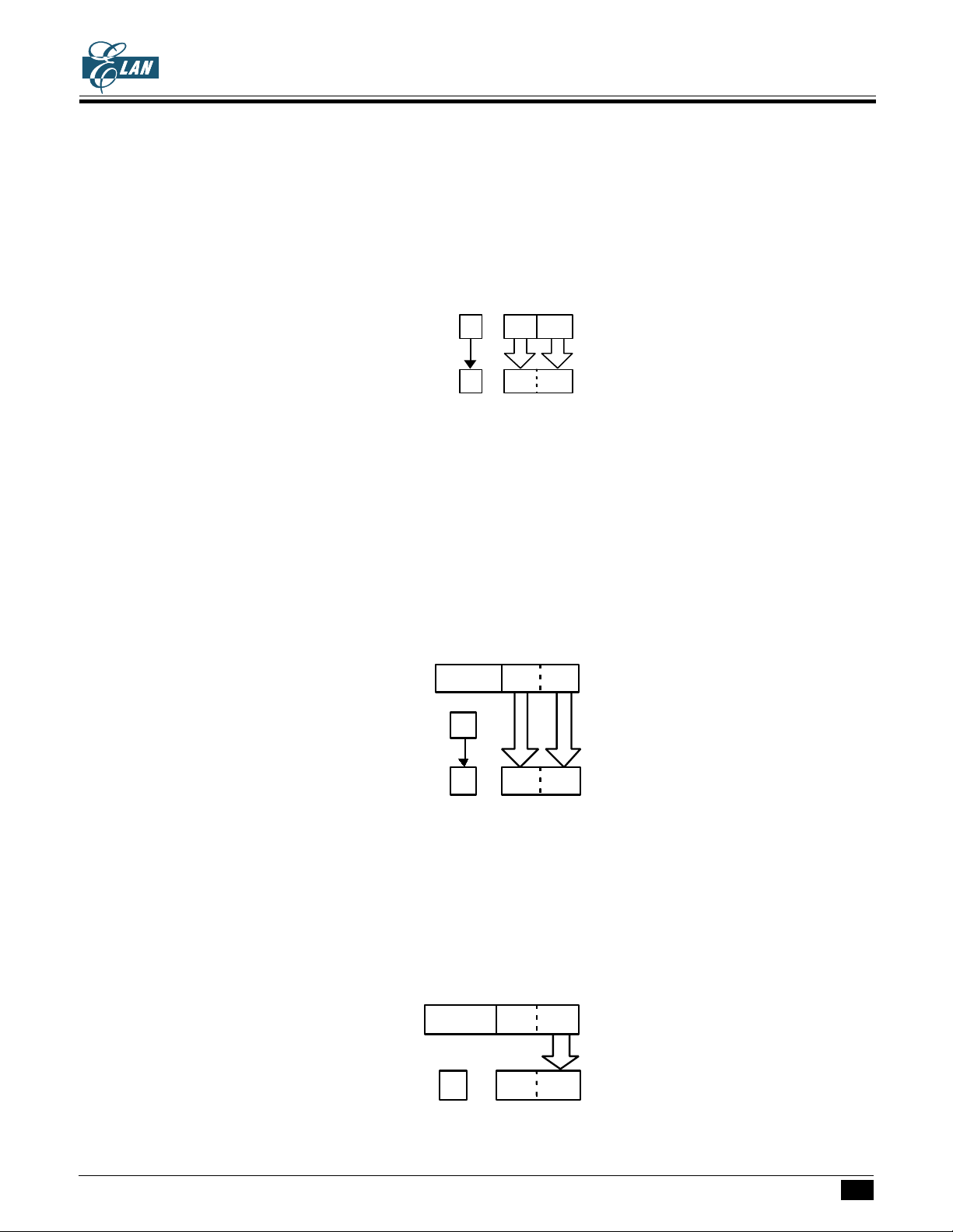
The bank is selected by P9.3. When P9.3 is cleared to "0", the bank 0 is selected, when P9.3 is set to "1", the bank
1 is selected.
The data Memory consists of three Address mode, namely -
(1) Indirect addressing mode:
The address in the bank is specified by the HL registers.
P9.3 HR LR
AM address
PROGRAM EXAMPLE: Load the data of RAM address "143h" to RAM address "023h".
SEP P9,3 ; P9.3← 1
LDL #3h ; LR← 3
LDH #4h ; HR← 4
LDAM ; Acc← RAM[134h]
CLP P9,3 ; P9.3← 0
LDL #2h ; LR← 2
LDH #3h ; HR← 3
STAM ; RAM[023h]← Acc
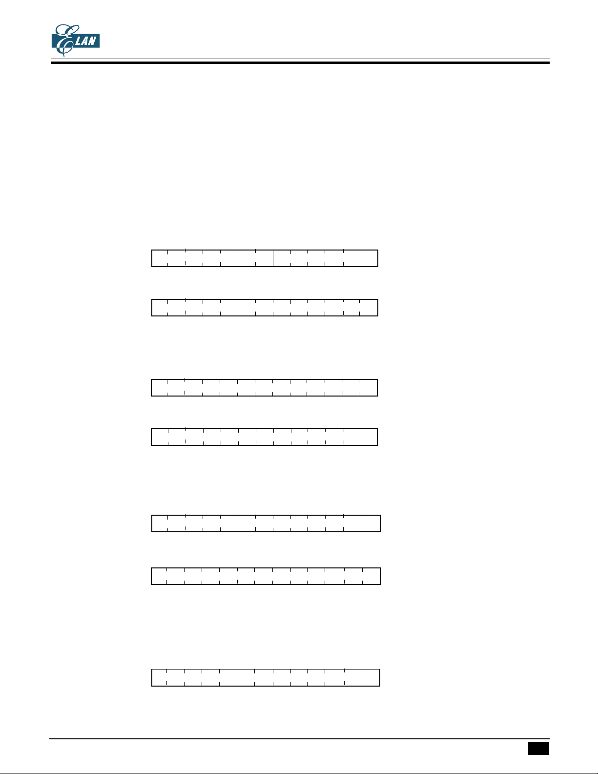
(2) Direct addressing mode:
The address in the bank is directly specified by 8 bits of the second byte in the instruction field.
instruction field
xxxxxxxx
P9.3
RAM address
PROGRAM EXAMPLE: Load the data of RAM address "143h" to RAM address "023h".
SEP P9,3 ; P9.3← 1
LDA 43h ; Acc← RAM[143h]
CLP P9,3 ; P9.3← 0
STA 23h ; RAM[023h]← Acc
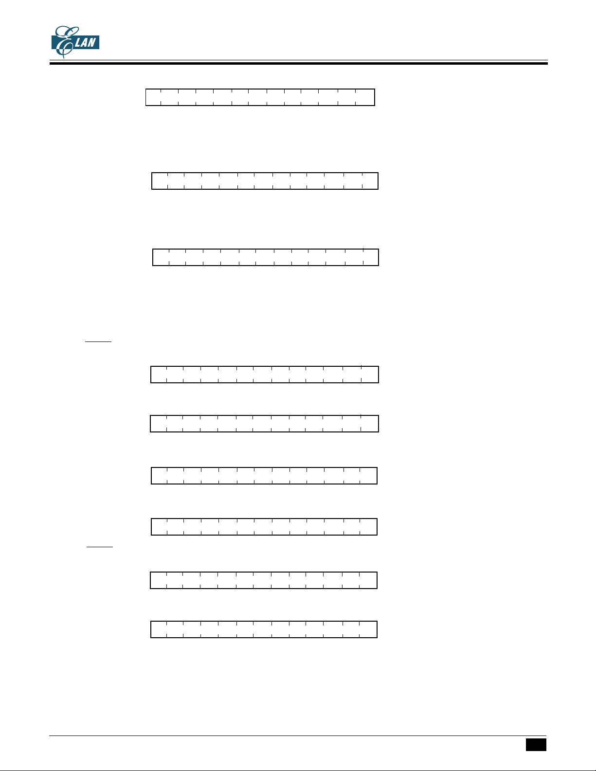
(3) Zero-page addressing mode:
The zero-page is in the bank 0 (address 000h~00Fh). The address is the lower 4 bits of the second byte in the
instruction field.
xxxxxxxx
instruction field
yyyy
RAM address
0
0000
yyyy
PROGRAM EXAMPLE: Write immediate "0Fh" to RAM address "005h".
STD #0Fh, 05h ; RAM[05h]← 0Fh
* This specification are subject to be changed without notice.
6.14.2001
7
Page 8
EM73963A
4-BIT MICRO-CONTROLLER FOR LCD PRODUCT
PROGRAM COUNTER (16K ROM)
Program counter ( PC ) is composed by a 13-bit counter, which indicates the next executed address for the
program ROM instruction.
For BRANCH and CALL instructions, PC is changed by instruction indicating. PC only can indicate the address
from 0000h-1FFFh. The bank number is decided by P3.
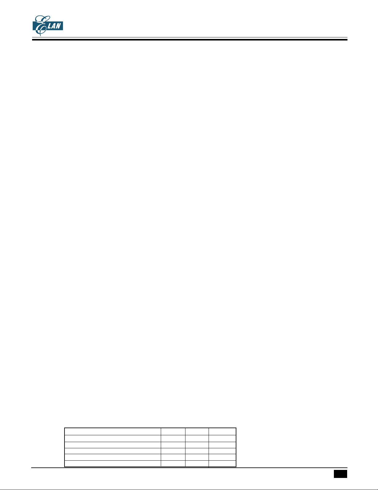
(1) Branch instruction:
SBR a
Object code: 00aa aaaa
Condition: SF=1; PC ← PC
PC Hold original PC value+1 aaaaaa
SF=0; PC← PC +1( branch condition not satisified)
PC Original PC value + 1
( branch condition satisified )
12-6.a
LBR a
Object code: 1100 aaaa aaaa aaaa
Condition: SF=1; PC ← PC
Hold
PC
a a a a a a aaaaaa
+2
( branch condition satisified )
12.a
SF=0; PC← PC +2( branch condition not satisified)
PC Original PC value + 2
SLBR a
Object code: 0101 0101 1100 aaaa aaaa aaaa (a:1000h~1FFFh)
0101 0111 1100 aaaa aaaa aaaa (a:0000h~0FFFh)
Condition: SF=1; PC ← a ( branch condition satisified)
PCaaaaaaaaaaaa a
SF=0 ; PC ← PC + 3 ( branch condition not satisified )
PC Original PC value + 3
(2) Subroutine instruction:
SCALL a
Object code: 1110 nnnn
Condition : PC ← a ; a=8n+6 ; n=1..Fh ; a=86h, n=0
PC00000aaaaa aaa
LCALL a
Object code: 0100 0aaa aaaa aaaa
Condition: PC ← a
* This specification are subject to be changed without notice.
6.14.2001
8
Page 9
EM73963A
4-BIT MICRO-CONTROLLER FOR LCD PRODUCT
PC00aaaaaaaaaa a
RET
Object code: 0100 1111
Condition: PC ← STACK[SP]; SP + 1
PC The return address stored in stack
RT I
Object code: 0100 1101
Condition : FLAG. PC ← STACK[SP]; EI ← 1; SP + 1
PC The return address stored in stack
(3) Interrupt acceptance operation:
When an interrupt is accepted, the original PC is pushed into stack and interrupt vector will be loaded into
PC,The interrupt vectors are as follows :
INT0 (External interrupt from P8.2)
PC00000000000 1 0
TRGA (Timer A overflow interrupt)
PC0000000000 1 1 0
TRGB (Time B overflow interrupt)
PC00000000 0 1 0 0 0
TBI (Time base interrupt)
PC00000000 0 1 0 1 0
INT1 (External interrupt from P8.0)
PC00000000 0 1 1 0 0
(4) Reset operation:
PC00000000000 0 0
(5) Other operations:
For 1-byte instruction execution: PC + 1
For 2-byte instruction execution: PC + 2
For 3-byte instruction execution: PC + 3
* This specification are subject to be changed without notice.
6.14.2001
9
Page 10
EM73963A
4-BIT MICRO-CONTROLLER FOR LCD PRODUCT
ACCUMULATOR
Accumulator is a 4-bit data register for temporary data storage. For the arithematic, logic and comparative
opertion .., ACC plays a role which holds the source data and result.
FLAGS
There are three kinds of flag, CF ( Carry flag ), ZF ( Zero flag ), and SF ( Status flag ), these three 1-bit flags
are included by the arithematic, logic and comparative .... operation.
All flags will be put into stack when an interrupt subroutine is served, and the flags will be restored after
RTI instruction is executed.
(1) Carry Flag ( CF )
The carry flag is affected by the following operations :
a. Addition : CF as a carry out indicator, under addition operation, when a carry-out occures, the CF is "1",
likewise, if the operation has no carry-out, the CF is "0".
b. Subtraction : CF as a borrow-in indicator, under subtraction operation, when a borrow occures, the CF
is "0", likewise, if there is no borrow-in, the CF is "1".
c. Comparision: CF as a borrow-in indicator for Comparision operation as the same as subtraction
operation.
d. Rotation: CF shifts into the empty bit of accumulator for the rotation and holds the shift out data after
rotation.
e. CF test instruction : Under TFCFC instruction, the CF content is sent into SF then clear itself as "0".
Under TTSFC instruction, the CF content is sent into SF then set itself as "1".
(2) Zero Flag ( ZF )
ZF is affected by the result of ALU, if the ALU operation generates a "0" result, the ZF is "1",
likewise, the ZF is "0".
(3) Status Flag ( SF )
The SF is affected by instruction operation and system status.
a. SF is initiated to "1" for reset condition.
b. Branch instruction is decided by SF, when SF=1, branch condition is satisified, likewise,
when SF=0, branch condition is unsatisified.
PROGRAM EXAMPLE:
Check following arithematic operation for CF, ZF, SF
CF ZF SF
LDIA #00h; - 1 1
LDIA #03h; - 0 1
ADDA #05h; - 0 1
ADDA #0Dh; - 0 0
ADDA #0Eh; - 0 0
* This specification are subject to be changed without notice.
6.14.2001
10
Page 11
EM73963A
4-BIT MICRO-CONTROLLER FOR LCD PRODUCT
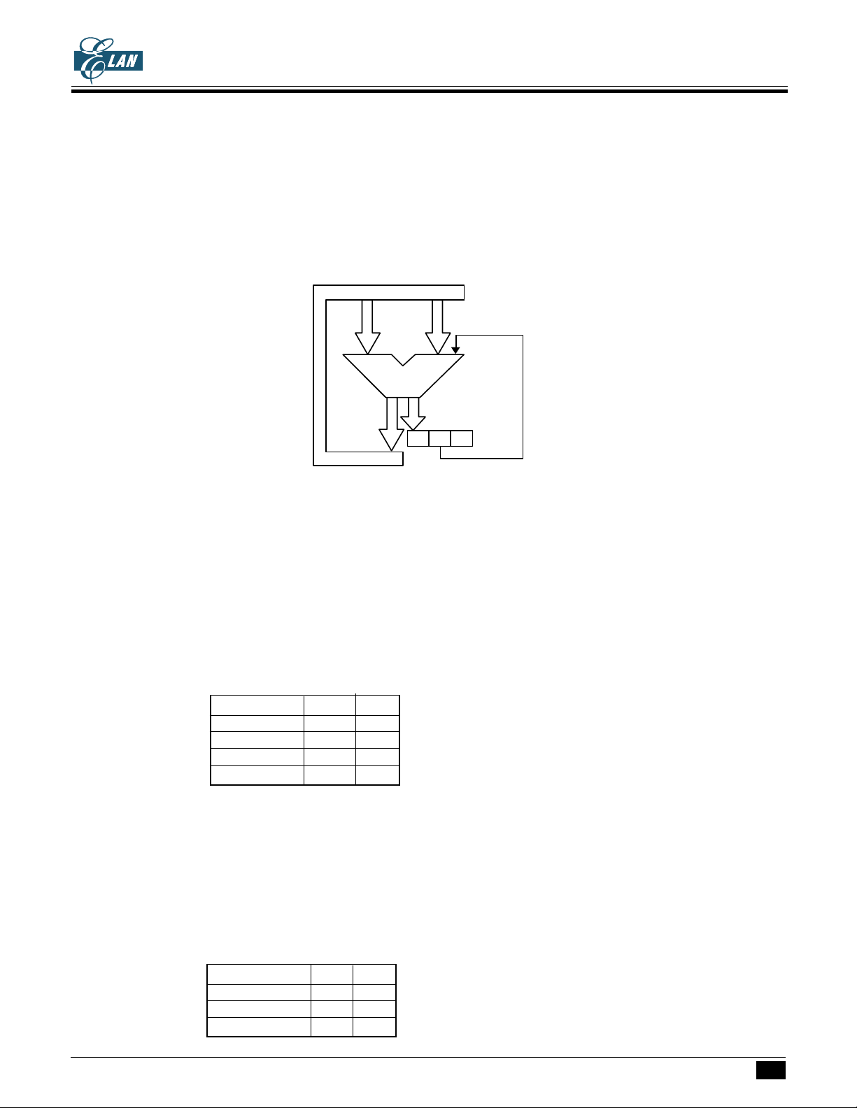
ALU
The arithematic operation of 4 - bit data is performed in ALU unit . There are 2 flags that can be affected by
the result of ALU operation, ZF and SF. The operation of ALU is affected by CF only.
ALU STRUCTURE
ALU supported user arithematic operation functions, including Addition, Subtraction and Rotaion.
DATA BUS
ALU
ZF CF SF
ALU FUNCTION
(1) Addition:
ALU supports addition function with instructions ADDAM, ADCAM, ADDM #k, ADD #k,y .... .
The addition operation affects CF and ZF. Under addition operation, if the result is "0", ZF will be "1",
otherwise, ZF will be "0", When the addition operation has a carry-out, CF will be "1", otherwise, CF will
be "0".
EXAMPLE:
Operation Carry Zero
3+4=7 0 0
7+F=6 1 0
0+0=0 0 1
8+8=0 1 1
(2) Subtraction:
ALU supports subtration function with instructions SUBM #k, SUBA #k, SBCAM, DECM.... The
subtraction operation affects CF and ZF, Under subtraction operation, if the result is negative, CF will be "0",
and a borrow out, otherwise, if the result is positive, CF will be "1". For ZF, if the result of subtraction
operation is "0", the ZF is "1", otherwise, ZF is "1".
EXAMPLE:
Operation Carry Zero
8-4=4 1 0
7-F= -8(1000) 0 0
9-9=0 1 1
* This specification are subject to be changed without notice.
6.14.2001
11
Page 12
EM73963A
4-BIT MICRO-CONTROLLER FOR LCD PRODUCT
(3) Rotation:
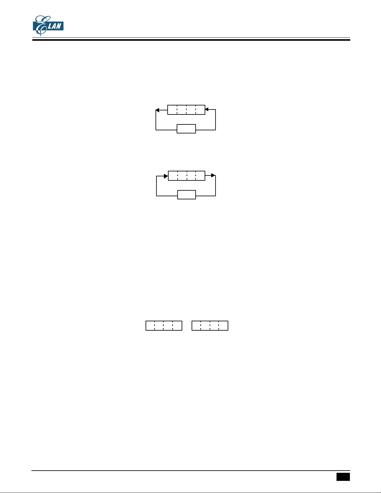
There are two kinds of rotation operation, one is rotation left, the other is rotation right.
RLCA instruction rotates Acc value to left, shift the CF value into the LSB bit of Acc and the shift out data
will be hold in CF.
MSB LSB
ACC
CF
RRCA instruction operation rotates Acc value to right, shift the CF value into the MSB bit of Acc and the
shift out data will be hold in CF.
MSB LSB
ACC
CF
PROGRAM EXAMPLE: To rotate Acc clockwise(right) and shift a "1" into the MSB bit of Acc.
TTCFS; CF ← 1
RRCA; rotate Acc right and shift CF=1 into MSB.
HL REGISTER
HL register are two 4-bit registers, they are used as a pair of pointer for the of RAM memory address. They
are used as also 2 independent temporary 4-bit data registers. For certain instructions, L register can be a pointer
to indicate the pin number (Port4 only).
HL REGISTER STRUCTURE
3 2 1 0
H REGISTER
HL REGISTER FUNCTION
(1) HL register is used as a temporary register for instructions : LDL #k, LDH #k, THA, THL, INCL, DECL,
EXAL, EXAH.
3 2 1 0
L REGISTER
PROGRAM EXAMPLE:
LDL #05h;
LDH #0Dh;
(2) HL register is used as a poiner for the address of RAM memory for instructions : LDAM, STAM, STAMI... .
PROGRAM EXAMPLE: Store immediate data "#0Ah" into RAM of address 35h.
LDL #5h;
LDH #3h;
STDMI #0Ah; RAM[35] ← Ah
* This specification are subject to be changed without notice.
Load immediate data "5h" into L register, "0Dh" into H register.
6.14.2001
12
Page 13
EM73963A
4-BIT MICRO-CONTROLLER FOR LCD PRODUCT
(3) L register is used as a pointer to indicate the bit of I/O port for instructions : SELP, CLPL, TFPL.
(When LR = 0 indicate P4.0)
PROGRAM EXAMPLE: To set bit 0 of Port4 to "1"
LDL #00h;
SEPL ; P4.0 ← 1
STACK POINTER (SP)
Stack pointer is a 4-bit register which stores the present stack level number.
Before using stack, user must set the SP value first, CPU will not initiate the SP value after reset condition.
When a new subroutine is received, the SP is decreased by one automatically, likewise, if returning from
a subroutine, the SP is increased one.
The data transfer between ACC and SP is done with instructions "LDASP" and "STASP".
DATA POINTER (DP)
Data pointer is a 12-bit register that stores the ROM address can indicating the ROM code data
specified by user (refer to data ROM).
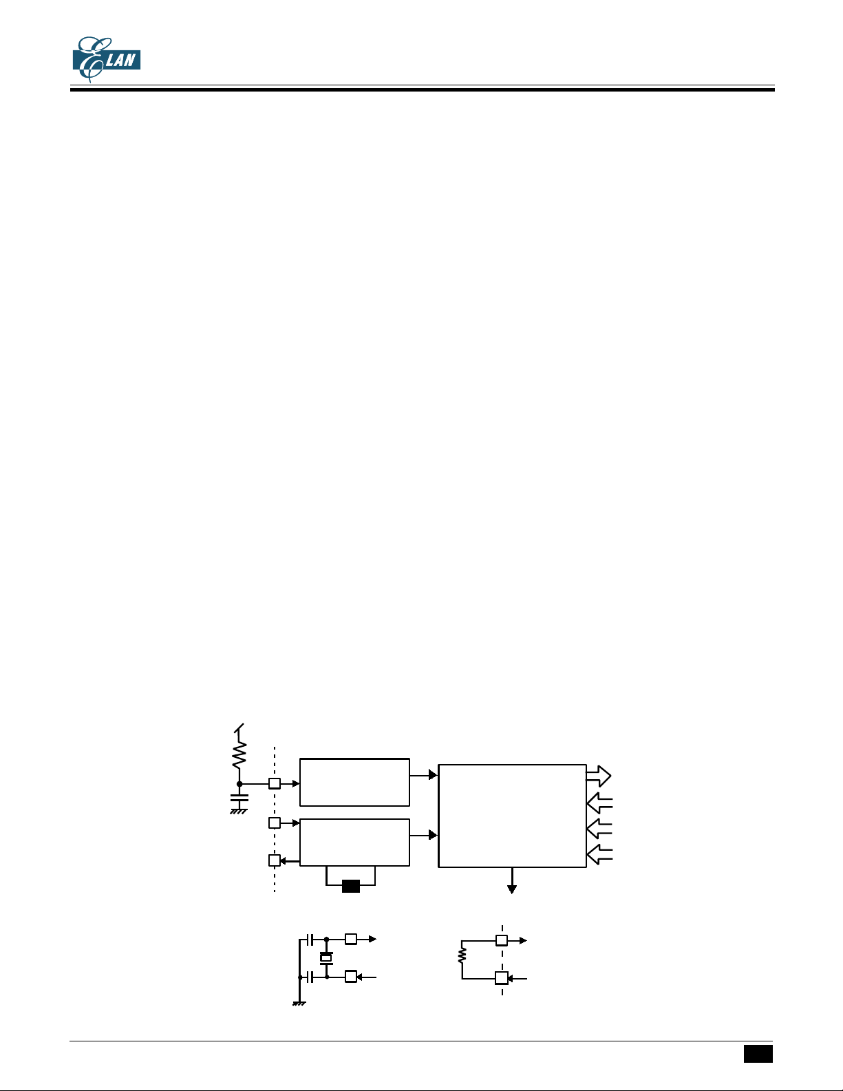
CLOCK AND TIMING GENERATOR
The clock generator is supported by a dual clock system. The high-frequency oscillator is source from RC
oscillator, the working frequency range is 480 KHz to 4 MHz defined by the mask option. The lowfrequency oscillator may be sourced from crystal or RC oscillator as defined by mask option, the working
frequency is 32 KHz.
CLOCK GENERATOR STRUCTURE
There are two clock generator for system clock control unit, P14 is the status register that hold the CPU
status. P16, P19 and P22 are the command register for system clock mode control
CLK
LXIN
LXOUT
High-frequency
generator
Low-frequency
generator
fc
System clock
fs
mode control
P14
P16
P19
P22
Mask option for choose Crystal or RC oscillator
LXIN
LXOUT
Crystal connection
* This specification are subject to be changed without notice.
System control
LXIN
LXOUT
RC connection
6.14.2001
13
Page 14
EM73963A
4-BIT MICRO-CONTROLLER FOR LCD PRODUCT
SYSTEM CLOCK MODE CONTROL
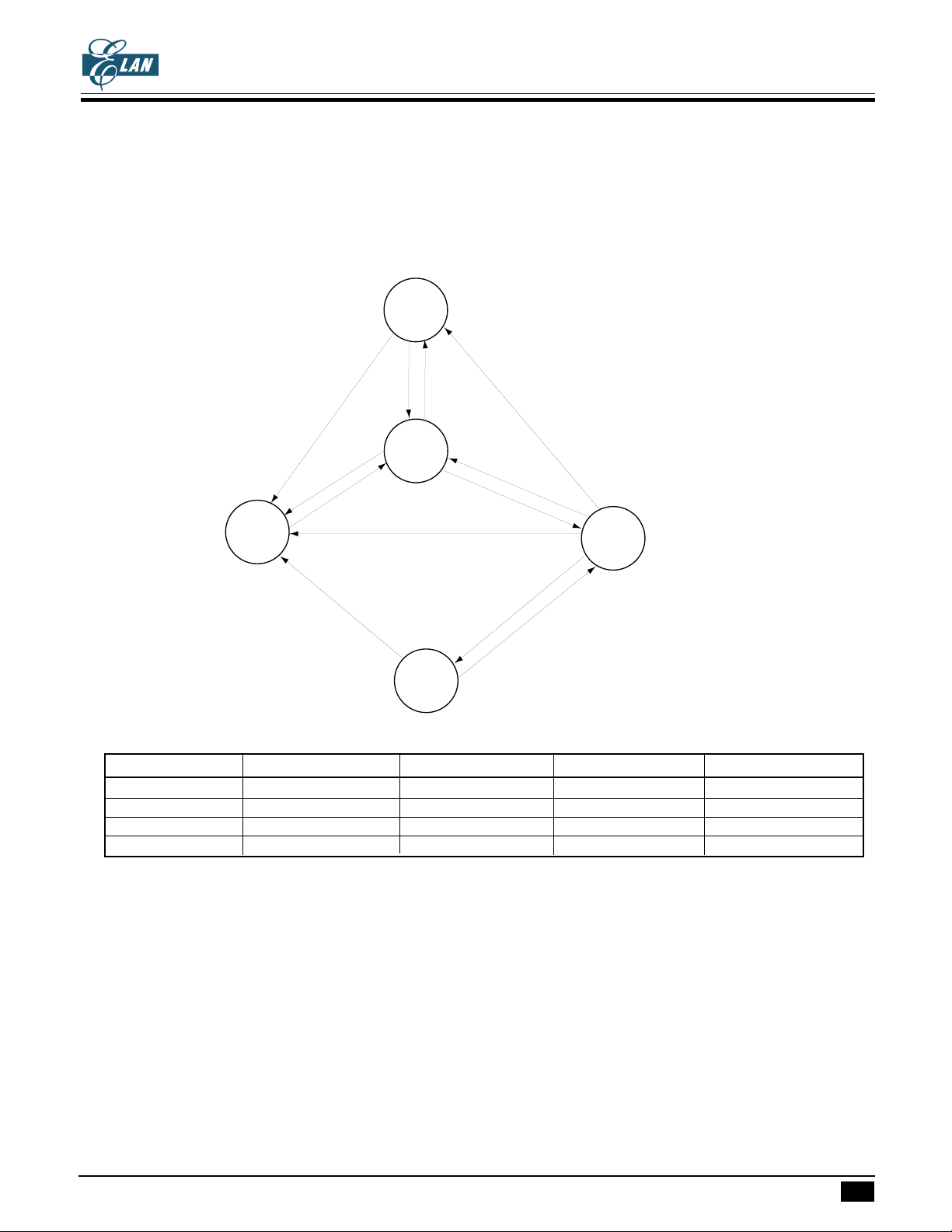
The system clock mode controller can start or stop the high-frequency and low-frequency clock oscillator
and switch between the basic clocks. EM73963A has four operation modes (DUAL, SLOW,IDLE and
STOP operation modes).
RESET
operation
Reset
Reset
I/O wakeup
Reset
Reset release
STOP
operation
mode
DUAL
operation
mode
Reset
IDLE
(CPU
stops)
Command
High osc : stopped
Low osc : stopped
(P16)
High osc : oscillating
Low osc : oscillating
Command
Command
(P22)
High osc : stopped
Low osc : oscillating
(P22)
Command
(P16)
Command
(P19)
I/O or internal timer wakeup
SLOW
operation
mode
High osc : stopped
Low osc : oscillating
Operation Mode Oscillator System Clock Available function One instruction cycle
DUAL High, Low frequency High frequency clock LCD, sound generator 8 / fc
SLOW Low frequency Low frequency clock LCD 8 / fs
IDLE Low frequency CPU stops LCD STOP None CPU stops All disable -
DUAL OPERATION MODE
The 4-bit µc is in the DUAL operation mode when the CPU is reseted. This mode is dual clock system
(high-frequency and low-frequency clocks oscillating). It can be changed to SLOW or STOP operation
mode with the command register (P22 or P16).
LCD display and sound generator are available for the DUAL operation mode.
SLOW OPERATION MODE
The SLOW operation mode is single clock system (low-frequency clock oscillating). It can be changed to
the DUAL operation mode with the command register (P22), STOP operation mode with P16 and IDLE
operation mode with P19.
LCD display is available for the SLOW operation mode.
* This specification are subject to be changed without notice.
6.14.2001
14
Page 15
4-BIT MICRO-CONTROLLER FOR LCD PRODUCT
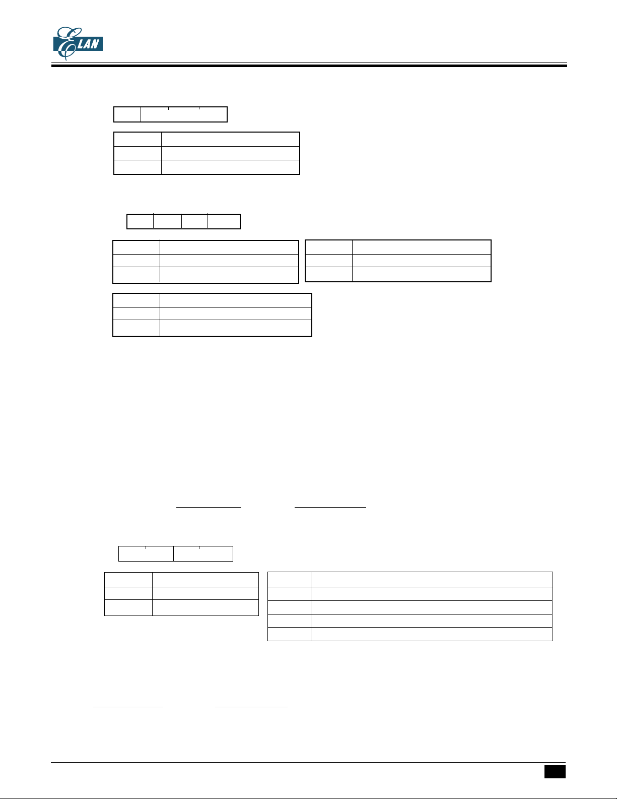
P22 32 1 0 Initial value : 0000
* SOM
SOM Select operation mode
0 0 0 DUAL operation mode
1 * * SLOW operation mode
P14 32 10 Initial value : *000
* WKS LFS CPUS
LFS Low-frequency status CPUS CPU status
0 LXIN source is not stable 0 DUAL operation mode
1 LXIN source is stable 1 SLOW operation mode
WKS Wakeup status
0 Wakeup not by internal timer
1 Wakeup by internal timer
EM73963A
Port14 is the status register for CPU. P14.0 (CPU status) and P14.1 (Low-frequency status) are read-only
bits. P14.2 (wakeup status) will be set as '1' when CPU is waked by internal timer. P14.2 will be cleared as
'0' when user out data to P14.
IDLE OPERATION MODE
The IDLE operation mode suspends all CPU functions except the low-frequency clock oscillation and the
LCD driver. It keeps the internal status with low power consumption without stopping the slow clock
oscillation and LCD display.
LCD display is available for the IDLE operation mode. Sound generator is disabled in this mode. The IDLE
operation mode will be wakeup and return to the SLOW operation mode by the internal timing generator or
I/O pins (P0(0..3)/WAKEUP 0..3 or P8(0..3)/WAKEUPA..D).
P19 32 10 Initial value : 0000
* IDME SIDR
IDME Enable IDLE mode SIDR Select IDLE releasing condition
1 Enable IDLE mode 0 0 P0(0..3), P8(0..3) pin input
0 no function 0 1 P0(0..3), P8(0..3) pin input and 1 sec signal
1 0 P0(0..3), P8(0..3) pin input and 0.5 sec signal
1 1 P0(0..3), P8(0..3) pin input and 15.625 ms signal
STOP OPERATION MODE
The STOP operation mode suspends system operation and holds the internal status immediately before the
suspension with low power consumption. This mode will be released by reset or I/O pins (P0(0..3)/
WAKEUP 0..3 or P8(0..3)/WAKEUP A..D).
LCD display and sound generator are disabled in the STOP operation mode.
* This specification are subject to be changed without notice.
6.14.2001
15
Page 16
EM73963A
4-BIT MICRO-CONTROLLER FOR LCD PRODUCT
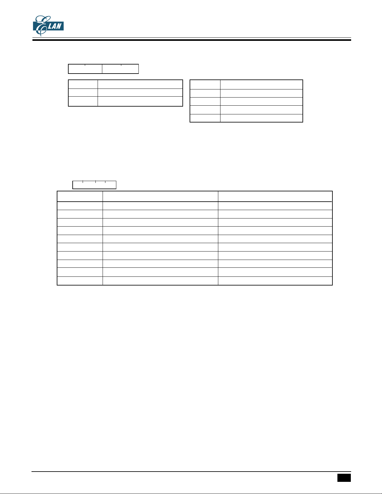
P16 3210 Initial value : 0000
* SPME SWWT
SPME Enable STOP mode SWWT Set wake-up warm-up time
1 Enable STOP mode 0 0 218/CLK
0 no function 0 1 2
10 216/CLK
1 1 no function
TIME BASE INTERRUPT (TBI )
The time base can be used to generate a single fixed frequency interrupt. Eight types of frequencies can be
selected with the "P25" setting.
P25 3 2 1 0
i
nitial value : 0000
P25 DUAL operation mode SLOW operation mode
0 0 x x Interrupt disable Interrupt disable
0 1 0 0 Interrupt frequency LXIN / 2
3
Hz Reserved
0 1 0 1 Interrupt frequency LXIN / 24 Hz Reserved
0 1 1 0 Interrupt frequency LXIN / 25 Hz Reserved
0 1 1 1 Interrupt frequency LXIN / 2
14
Hz Interrupt frequency LXIN / 2
1 1 0 0 Interrupt frequency LXIN / 21 Hz Reserved
1 1 0 1 Interrupt frequency LXIN / 26 Hz Interrupt frequency LXIN / 26 Hz
1 1 1 0 Interrupt frequency LXIN / 28 Hz Interrupt frequency LXIN / 28 Hz
1 1 1 1 Interrupt frequency LXIN / 2
10
Hz Interrupt frequency LXIN / 2
1 0 x x Reserved Reserved
14
/CLK
14
10
Hz
Hz
TIMER / COUNTER ( TIMERA, TIMERB)
Timer/counters support three special functions:
1. Even counter
2. Timer.
3. Pulse-width measurement.
These three functions can be executed by 2 timer/counter independently.
With timerA, the counter data is saved in timer register TAH, TAM, TAL. User can set counter initial value
and read the counter value by instruction "LDATAH(M,L)" and "STATAH(M,L)". With timer B register
is TBH, TBM, TBL and the W/R instruction "LDATBH (M,L)" and "STATBH (M,L)".
The basic structure of timer/counter is composed by two identical counter module, these two modules can
be set initial timer or counter value to the timer registers, P28 and P29 are the command registers for timer
A and timer B, user can choose different operation modes and internal clock rates by setting these two registers.
When timer/counter overflows, it will generate a TRGA(B) interrupt request to interrupt control unit.
* This specification are subject to be changed without notice.
6.14.2001
16
Page 17
4-BIT MICRO-CONTROLLER FOR LCD PRODUCT
INTERRUPT CONTROL
EM73963A
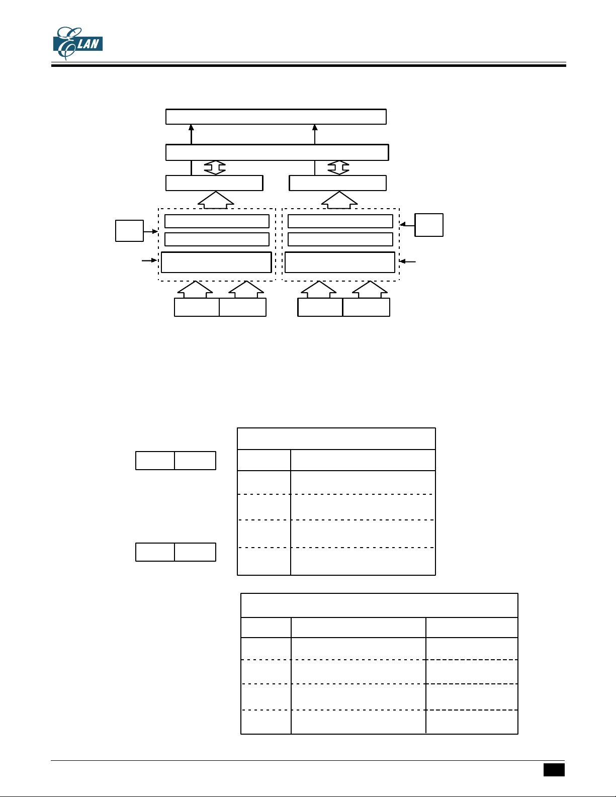
TRGA request
TRGB request
DATA BUS
P8.3/
TRGA
internal clock
12 BIT COUNTER
EVENT COUNTER CONTROL
TIMER CONTROL
PULSE-WIDTH MEASUREMENT
P28
CONTROL
TMSA IPSA
12 BIT COUNTER
EVENT COUNTER CONTROL
TIMER CONTROL
PULSE-WIDTH MEASUREMENT
P29
CONTROL
TMSB IPSB
P8.1/
TRGB
internal clock
TIMER/COUNTER CONTROL
P8.1/TRGB, P8.3/TRGA are the external timer inputs for timerB and timerA, they are used in event
counter and pulse-width measurement mode.
Timer/counter command port: P28 is the command port for timer/counterA and P29 is for the timer/
counterB.
Port 28
Port 29
3 2 1 0
TMSA IPSA
Initial state: 0000
3 2 1 0
TMSB IPSB
Initial state: 0000
TIMER/COUNTER MODE SELECTION
TMSA (B) Function description
0 0 Stop
0 1 Event counter mode
1 0 Timer mode
1 1 Pulse width measurement mode
INTERNAL PULSE-RATE SELECTION
IPSA(B) DUAL mode
0 0 LXIN/2 Hz
0 1 LXIN/2 Hz
1 0 LXIN/2 Hz
1 1 LXIN/2 Hz
3
7
11
15
SLOW mode
Reserved
LXIN/2 Hz
LXIN/2 Hz
LXIN/2 Hz
7
11
15
* This specification are subject to be changed without notice.
6.14.2001
17
Page 18
EM73963A
4-BIT MICRO-CONTROLLER FOR LCD PRODUCT
TIMER/COUNTER FUNCTION
Timer/counterA, B are can be programmable for timer, event counter and pulse width measurement mode.
Each timer/counter can execute any of these functions independently.
EVENT COUNTER MODE
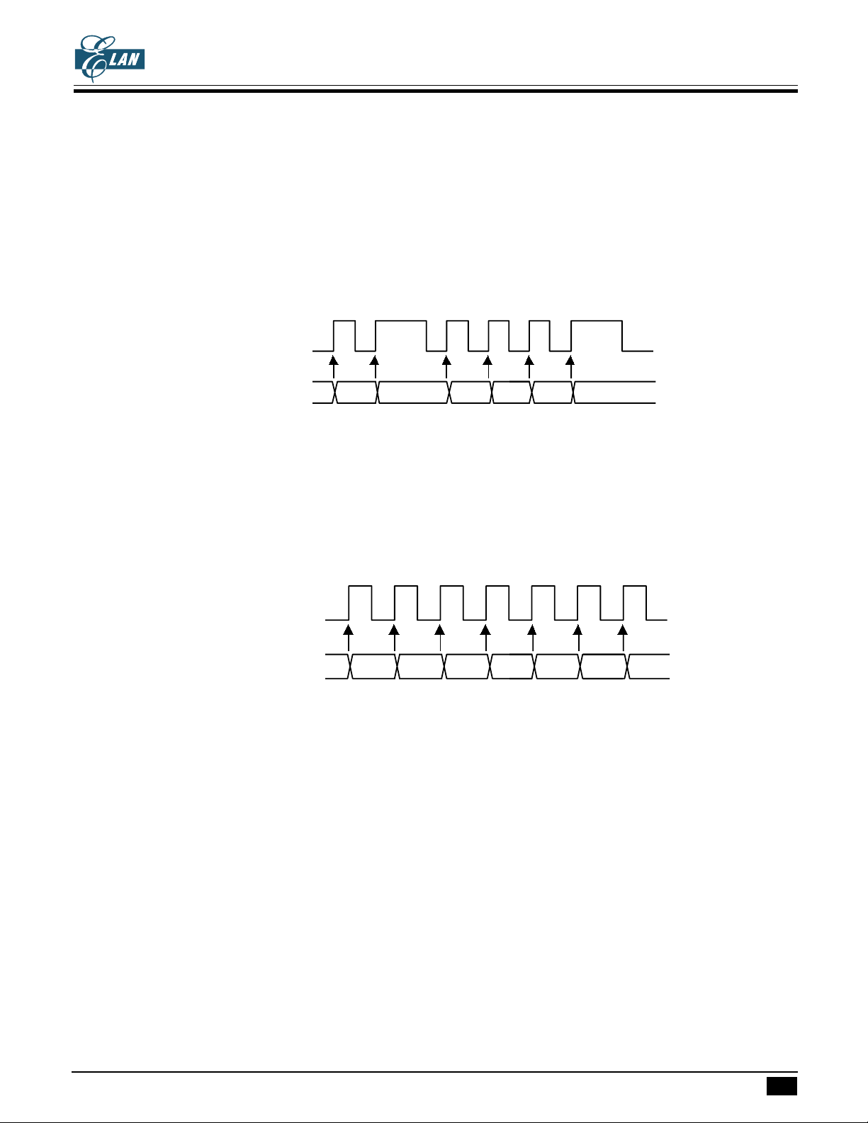
Under event counter mode, the timer/counter is increased by one at any rising edge of P8.1/TRGB for timerB
(P8.3/TRGA for timer A). When timerB (timerA) counts overflow, it will provide an interrupt request
TRGB (TRGA) to interrupt control unit.
P8.1/TRGB (P8.3/TRGA)
TimerB (TimerA) value n n+1 n+2 n+3 n+4 n+5 n+6
PROGRAM EXAMPLE: Enable timerA with P28
LDIA #0100b;
OUTA P28; Enable timerA with event counter mode
TIMER MODE
Under timer mode, the timer/counter is increased by one at any rising edge of internal pulse. User can choose
up to 4 types of internal pulse rate by setting IPSB for timerB (IPSA for timerA).
When timer/counter counts overflow, an interrupt request will be sent to interrupt control unit.
Internal pulse
TimerB (TimerA )value
n n+1 n+2 n+3 n+4 n+5 n+6
n+7
PROGRAM EXAMPLE: To generate TRGA interrupt request after 60 ms with system clock LXlN=32KHz
LDIA #0100B;
EXAE; enable mask 2
EICIL 110111b; interrupt latch ←0, enable EI
LDIA #0Ah;
STATAL;
LDIA #00h;
STATAM;
LDIA #0Fh;
STATAH;
LDIA #1000B;
OUTA P28; enable timerA with internal pulse rate: LXIN/23 Hz
NOTE: The preset value of timer/counter register is calculated as following procedure.
Internal pulse rate: LXIN/2
3
; LXIN = 32KHz
The time of timer counter count one = 23 /LXIN = 8/32768=0.244ms
The number of internal pulse to get timer overflow = 60 ms/ 0.244ms = 245.901= 0F6h
The preset value of timer/counter register = 1000h - 0F6h = F0Ah
PULSE WIDTH MEASUREMENT MODE
* This specification are subject to be changed without notice.
6.14.2001
18
Page 19
EM73963A
P
4-BIT MICRO-CONTROLLER FOR LCD PRODUCT
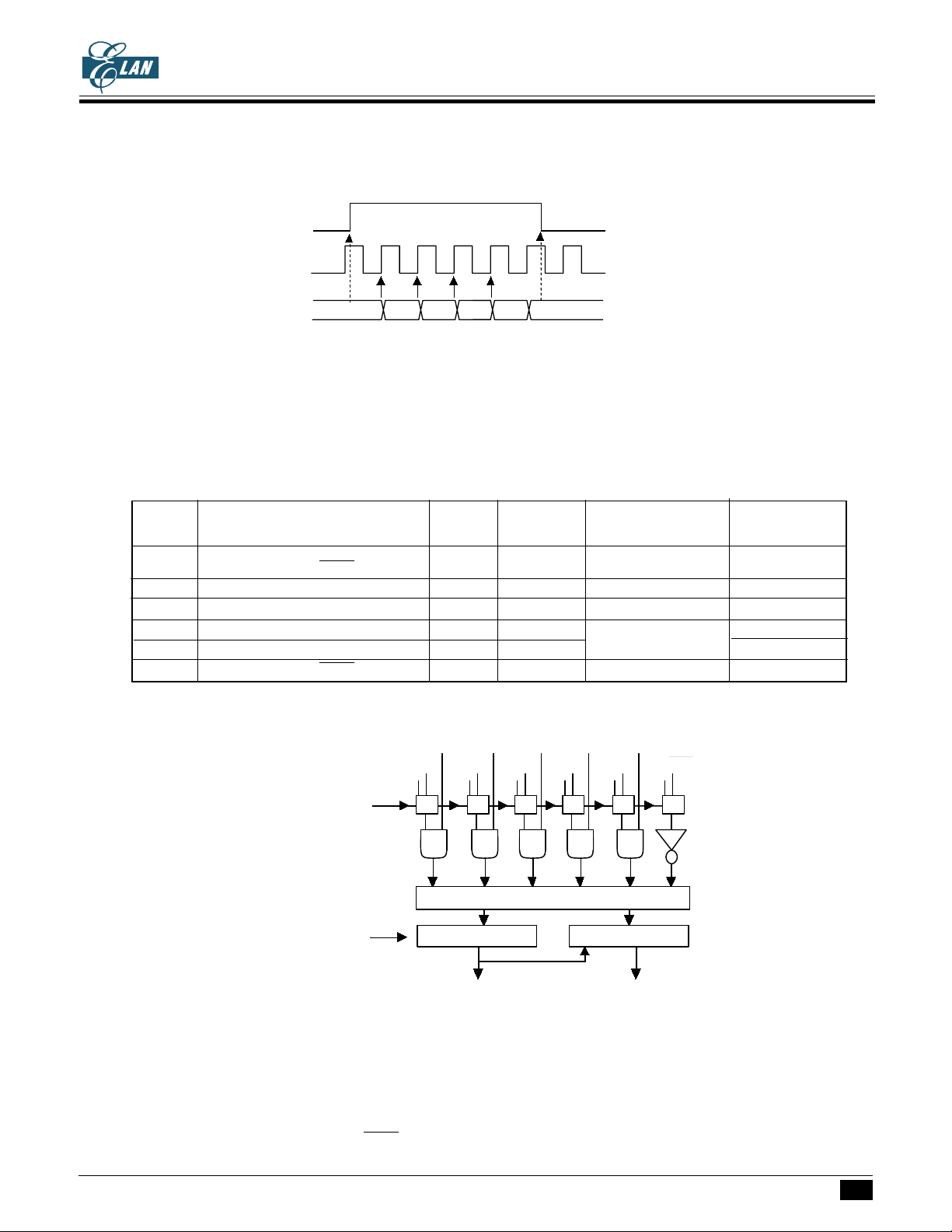
Under the pulse width measurement mode, the counter is incresed at the rising edge of internal pulse during
external timer/counter input (P8.1/TRGB, P8.3/TRGA ) in high level, interrupt request is generated as soon
as timer/counter count overflow.
8.1/TRGB(P8.3/TRGA)
Internal pulse
TimerB(TimerA) value
n n+1 n+2 n+3 n+4 n+5
PROGRAM EXAMPLE: Enable timerA by pulse width measurement mode.
LDIA #1100b;
OUTA P28; Enable timerA with pulse width measurement mode.
INTERRUPT FUNCTION
Five interrupt sources are available, 2 from external interrupt sources and 3 from internal interrupt sources.
Multiple interrupts are admitted according to their priority.
Type Interrupt source Priority Interrupt Interrupt Program ROM
Latch Enable condition entry address
External External interrupt(INT0) 1 IL5 EI=1 002h
Internal Reserved 2 IL4 EI=1, MASK3=1 004h
Internal TimerA overflow interrupt (TRGA) 3 IL3 EI=1, MASK2=1 006h
Internal TimerB overflow interrupt (TRGB) 4 IL2 EI=1, MASK1=1 008h
Internal Time base interrupt(TBI) 5 IL1 00Ah
External External interrupt(INT1) 6 IL0 EI=1,MASK0=1 00Ch
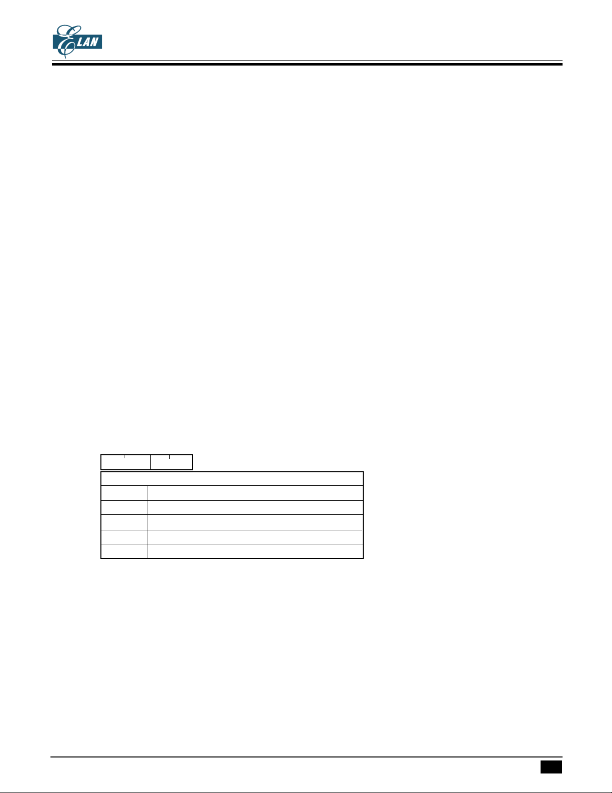
INTERRUPT STRUCTURE
MASK0 MASK1 MASK1 MASK2 MASK3
TRGA
r2
r3
IL2
IL3
r4
IL4
INT0
r5
IL5
Reset by system reset and program
instruction
INT1
r0
IL0
TRGB Reserved
TBI
r1
IL1
Priority checker
Reset by system reset and program
instruction
Set by program instruction
EI Entry address generator
Interrupt request Interrupt entry address
Interrupt controller:
IL0-IL5 : Interrupt latch. Hold all interrupt requests from all interrupt sources. IL's can not
be set by program, but can be reset by program or system reset, so IL can only
decide which interrupt source can be accepted.
MASK0-MASK3 : Except INT0 ,MASK register may promit or inhibit all interrupt sources.
* This specification are subject to be changed without notice.
6.14.2001
19
Page 20
4-BIT MICRO-CONTROLLER FOR LCD PRODUCT
EI : Enable interrupt Flip-Flop can promit or inhibit all interrupt sources, when interrupt
occurs, EI is auto cleared to "0" , after RTI instruction is executed, EI is auto set to
"1" again .
Priority checker: Check interrupt priority when multiple interrupts occur.
INTERRUPT FUNCTION
The procedure of interrupt operation:
1. Push PC and all flags to stack.
2. Set interrupt entry address into PC.
3. Set SF= 1.
4. Clear EI to inhibit other interrupts occur.
5. Clear the IL with which interrupt source has already been accepted.
6. Excute interrupt subroutine from the interrupt entry address.
7. CPU accept RTI, restore PC and flags from stack . Set EI to accept other interrupt requests.
PROGRAM EXAMPLE: To enable interrupt of "INT0, TRGA"
LDIA #1100B;
EXAE; set mask register "1100B"
EICIL 010111B ; enable interrupt F.F and clear IL3 and IL5.
EM73963A
LCD DRIVER
It can directly drive the liquid crystal display ( LCD ) and has 40 segments , 8 commons output pins.
There are total 40x8 dots can be display. The V1~V4 are the LCD bias voltage input pins.
(1) LCD driver control command register:
Port27 3210 Initial value: 0000
LDC * *
LCD DISPLAY CONTROL
LDC Function description
0 0 LCD display disable
0 1 Blanking
1 0 no function
1 1 LCD display enable
* : Don't care .
P27 is the LDC driver control command register . The initial value is 0000 .
When LDC ( bit2 and bit3 of P27 ) is set to "00", the LCD display is disabled .
When LDC is set to "01", the LCD is blanking, the COM pins are inactive and the SEG pins output the display
data continuously .
When LDC is set to "11", the LCD display is enabled.
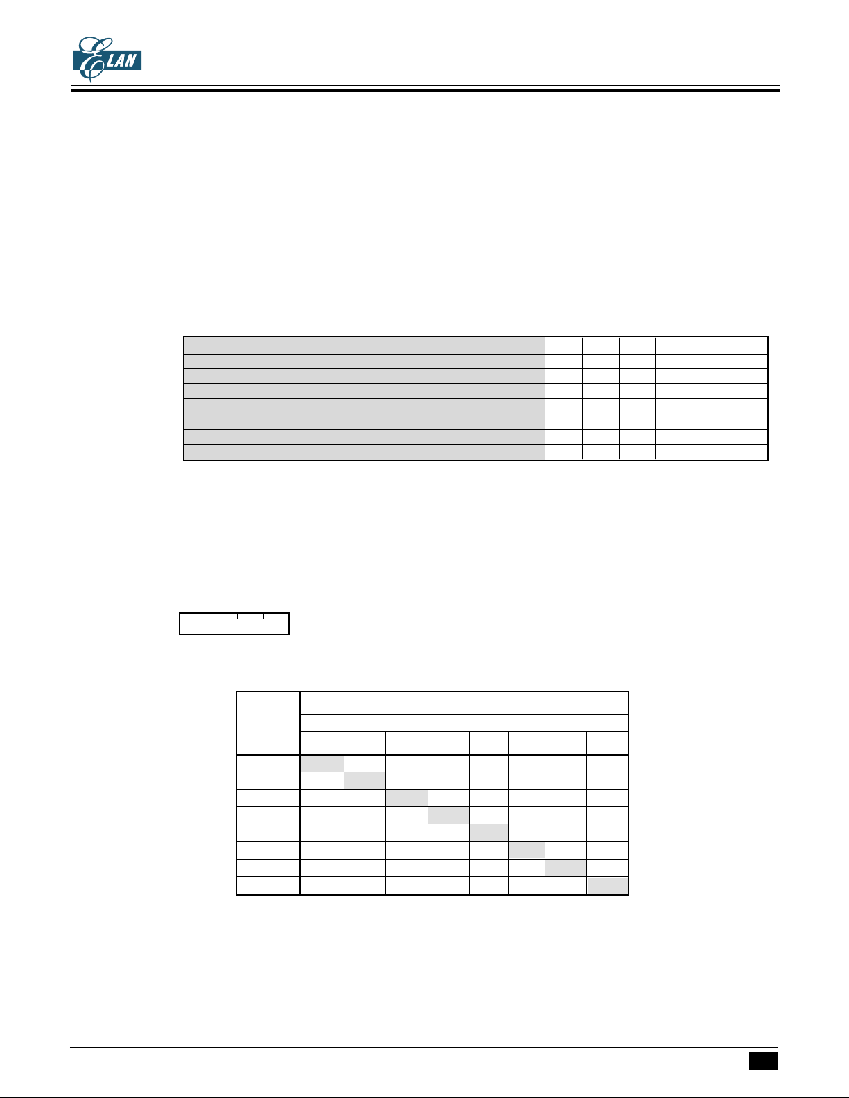
(2) LCD display data area:
The LCD display data is stored in the display data area of the data memory ( RAM) . The LCD display data
area is as illustrated below:
* This specification are subject to be changed without notice.
6.14.2001
20
Page 21
EM73963A
4-BIT MICRO-CONTROLLER FOR LCD PRODUCT
The display data from the display data area are automatically read out and send to the LCD driver directly by
the hardware. Therefore, the display patterns can be changed only by overwritting the contents of the
display data area through software.
The display memory area that is not used to store the LCD display data could be used as the ordinary data
memory.
LCD display data area :
Bank1
P9.3=1
012345 6789
100-10Fh
110-11Fh
120-12Fh
130-13Fh
140-14Fh
150-15Fh
160-16Fh
170-17Fh
SEG0
SEG1
SEG2
SEG3
SEG4
SEG5
SEG6
SEG7
SEG8
SEG9
SEG10
SEG11
SEG12
SEG13
SEG14
SEG15
SEG16
COM0
COM1
COM2
COM3
COM4
COM5
COM6
COM7
SEG17
SEG18
SEG19
SEG20
SEG21
SEG22
SEG23
SEG24
SEG25
SEG26
SEG27
P26 is the start address register of LCD common pin.
Port26 3 2 1 0 Initial value: *000
* CSA
Common start address register
CSA
X000
X001
X010
X011
X100
X101
X110
X111
100109h
COM0
COM7
COM6
COM5
COM4
COM3
COM2
COM1
110119h
COM1
COM0
COM7
COM6
COM5
COM4
COM3
COM2
120129h
COM2
COM1
COM0
COM7
COM6
COM5
COM4
COM3
RAM
130139h
COM3
COM2
COM1
COM0
COM7
COM6
COM5
COM4
SEG28
SEG29
SEG30
SEG31
SEG32
140149h
COM4
COM3
COM2
COM1
COM0
COM7
COM6
COM5
SEG33
SEG34
SEG35
SEG36
SEG37
150159h
COM5
COM4
COM3
COM2
COM1
COM0
COM7
COM6
ABCDEF
SEG38
SEG39
160-
170-
169h
179h
COM6
COM5
COM4
COM3
COM2
COM1
COM0
COM7
COM7
COM6
COM5
COM4
COM3
COM2
COM1
COM0
* This specification are subject to be changed without notice.
6.14.2001
21
Page 22
EM73963A
4-BIT MICRO-CONTROLLER FOR LCD PRODUCT
PROGRAM EXAMPLE:
LDIA #0000B
OUTA P26
LDIA #1100B ; LCD display enable
OUTA P27
LDIA #1010B ; store 1010B to RAM[101h]
SEP P9,3
STA 01H
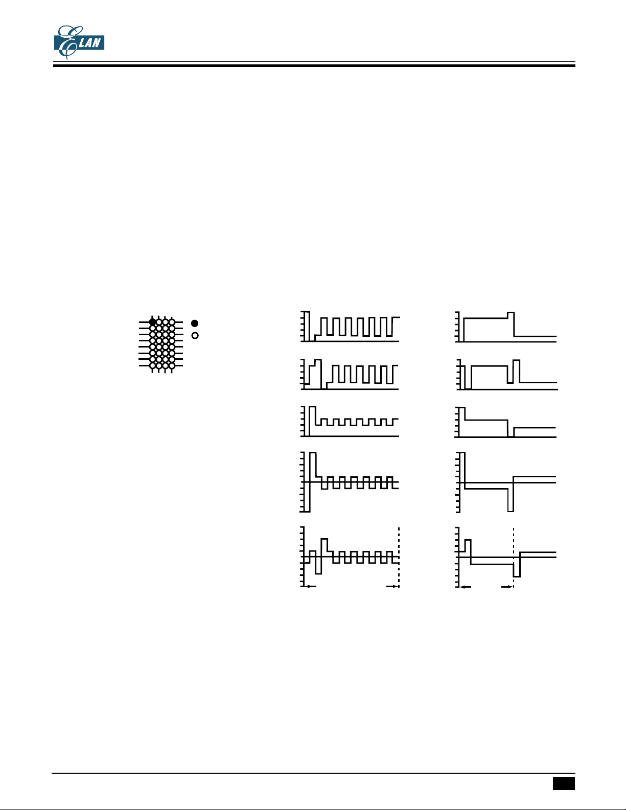
(3) LCD waveform : (1/5 bias)
Although there are two LCD waveform types, but for the reason of the number of voltage transition
point in type A is greater than type B, so type B gets a better display performance.
COM0
COM7
S
E
G
0
: ON
: OFF
* TYPE A :
COM0
VDD
V4
V3
V2
V1
Vss
COM1
SEG0
SEG0-COM0
ON
SEG0-COM1
OFF
* TYPE B :
COM0
VDD
V4
V3
V2
V1
Vss
COM1
SEG0
SEG0-COM0
ON
SEG0-COM1
OFF
Frame freq.=64Hz
Frame freq.
=64Hz
(4) LCD bias resistor :
There are high and low resistance choices for LCD bias resistor. To choose low bias resistor will take more power
but get a better display performance.
(5) LCD bias supply :
The LCD bias voltage can be supplied by bias resistor. When user chooses a large bias resistor or uses a large
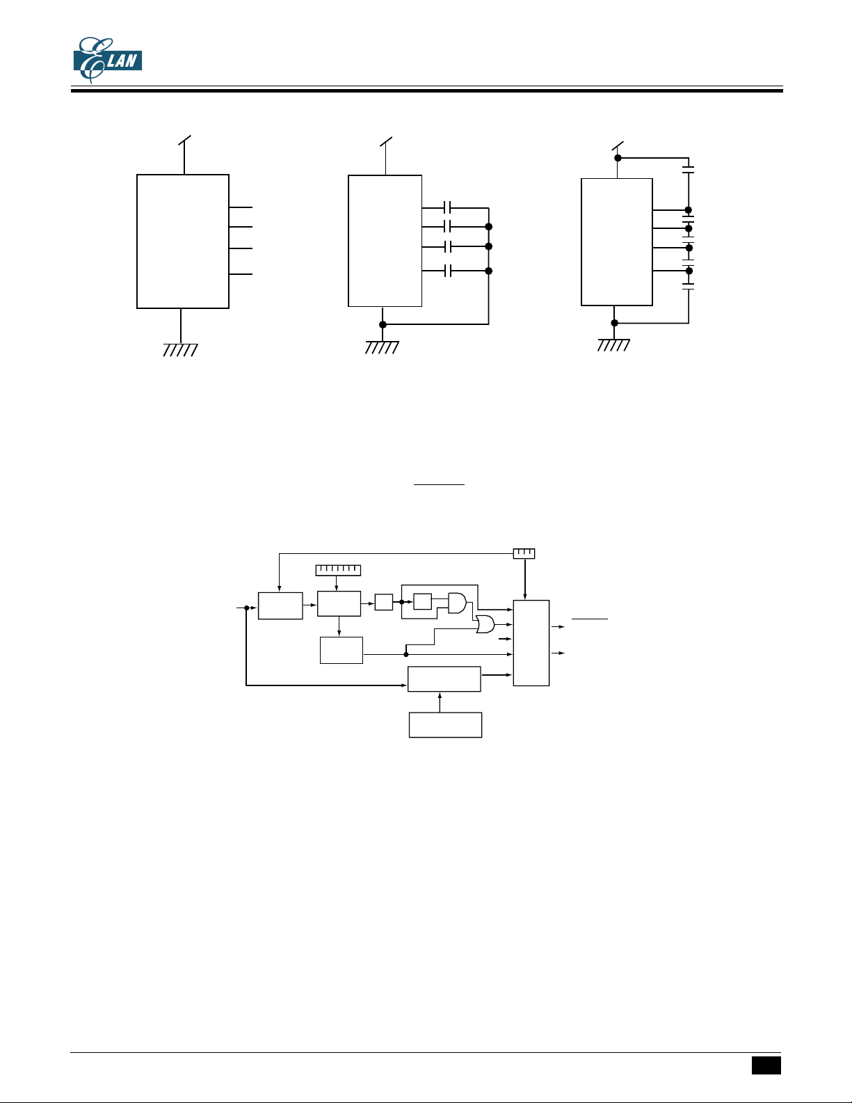
LCD panel, to connect 4 capacitors to V1~V4 can get a better display performance. Otherwise, you can open
V1~V4 and ignore these 4 capacitors.
* This specification are subject to be changed without notice.
6.14.2001
22
Page 23
EM73963A
4-BIT MICRO-CONTROLLER FOR LCD PRODUCT
0.1µF
V
VDD
VSS
V1
V2
V3
V4
or or
DD
V1
V2
0.1µF
0.1µF
0.1µF
V3
V4
V
SS
0.1µF
SOUND EFFECT
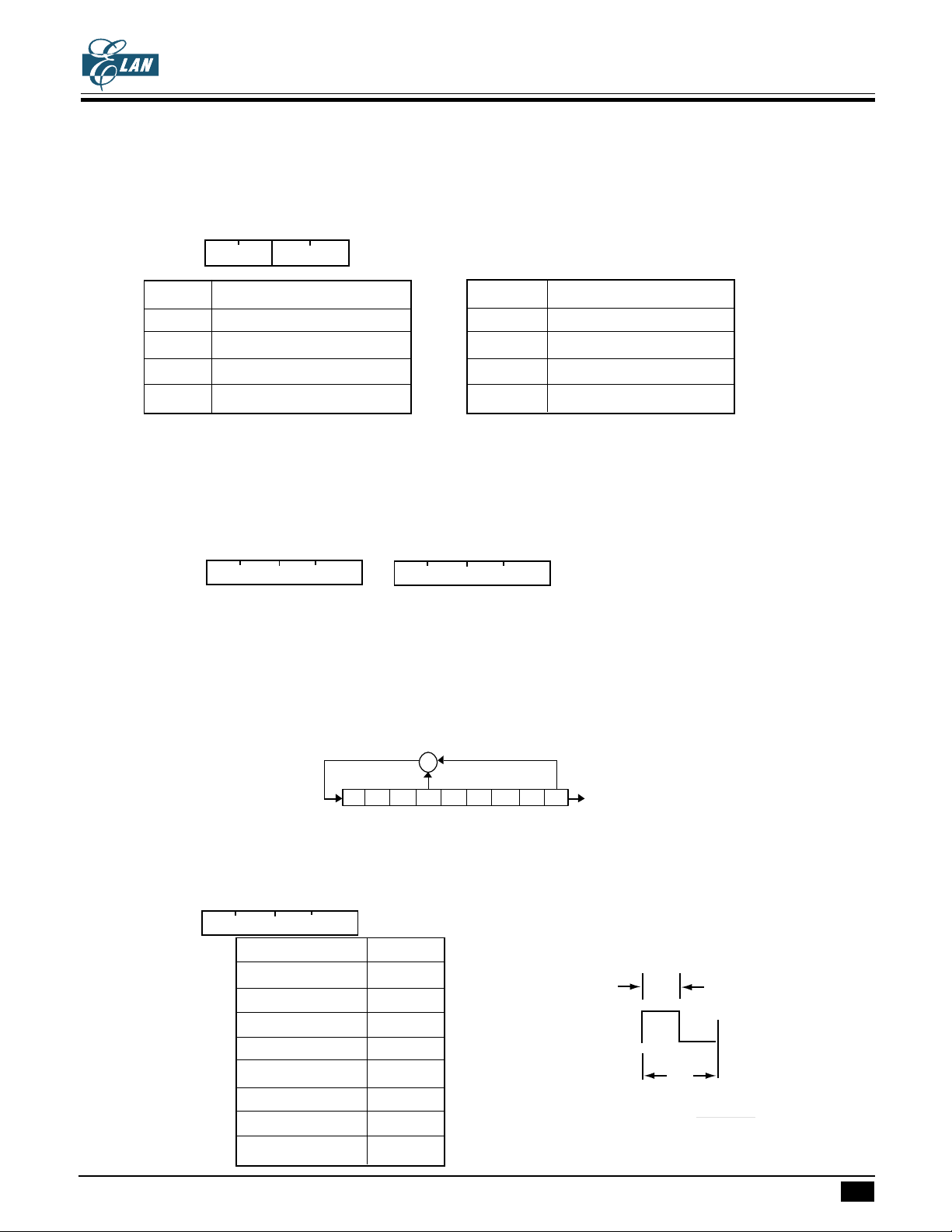
EM73963A has a built-in sound effect generator. It includes the tone generator, random generator and volume
control. The tone generator is a binary down counter and random generator is a 9-bit linear feedback shift register.
The sound generator is available for the DUAL mode. When the CPU is reseted or in the IDLE or STOP operation
mode, the sound generator is disable and the P4.0/SOUND is in high state and SOUND is in low state.
V
DD
V1
V2
0.1µF
0.1µF
V3
V4
V
SS
0.1µF
0.1µF
240KHz
3 kinds
of divider
f1
Tone
generator
Random
generator
f2x2
P23,P24
f2
÷2
÷2
PWM
volume control
High
Output
control
P30
SOUND
SOUND
* This specification are subject to be changed without notice.
6.14.2001
23
Page 24
EM73963A
tp
ts
tp=
60KHz
1
4-BIT MICRO-CONTROLLER FOR LCD PRODUCT
Sound generator command register
Three basic frequencies for sound generator can be selected by P30. The output of sound effect generator can
be tone, random tone or both combination.
Port30 3 2 1 0
BFREQ SMODE Initial value : 0000
BFREQ Basic frequency (f1) select SMODE Sound generator mode
0 0 240 KHz 0 0 Disable
0 1 120 KHz 0 1 Tone output
1 0 60 KHz 1 0 Random output
1 1 don't care 1 1 Tone+random output
Tone frequency register
The 8-bit tone frequency register (TF) is P24 and P23. The tone frequency will be changed when user output
the different data to P24 and P23.
Port24 Port23
3 2 1 0 3 2 1 0 Initial value : 1111 1111
Higher nibble register Lower nibble register
** f1=240K/2X, f2=f1/(TF+1)/2, TF=1~255, TF0
** Example : BFREQ=10, TF=00110001B.
⇒ f1=60K Hz, f2=60K Hz/50/2=600 Hz
Random generator
f(x)=x9+x4+1
+
123456789
Volume control register
The are 8 volume levels for sound generator. P17 is the volume control register.
Port17
Initial value : * 111
3 2 1 0
* VCR
VCR ts/tp
111 8/8
110 7/8
101 6/8
100 5/8
011 4/8
010 3/8
001 2/8
000 1/8
* This specification are subject to be changed without notice.
6.14.2001
24
Page 25
EM73963A
4-BIT MICRO-CONTROLLER FOR LCD PRODUCT
PROGRAM EXAMPLE:
LDIA #1001B ; basic frequency : 60 KHz tone output
OUTA P30
LDIA #0011B ; volume control
OUTA P17
LDIA #0011B ; 600 Hz tone output
OUTA P24
LDIA #0001B
OUTA P23
RESETTING FUNCTION
When CPU in normal working condition and RESET pin is held in low level for three instruction cycles at least,
then CPU begins to initialize the whole internal states, when RESET pin changes to high level, CPU begins
to work in normal condition.
The CPU internal state during reset condition is as following table :
Hardware condition in RESET state Initial value
Program counter 0000h
Status flag 01h
Interrupt enable flip-flop ( EI ) 00h
MASK0 ,1, 2, 3 00h
Interrupt latch ( IL ) 00h
P3, 9, 14, 16, 17, 19, 22, 25, 26, 27, 28, 29, 30 00h
P4, 8, 17, 23, 24 0Fh
CLK, LXIN Start oscillation
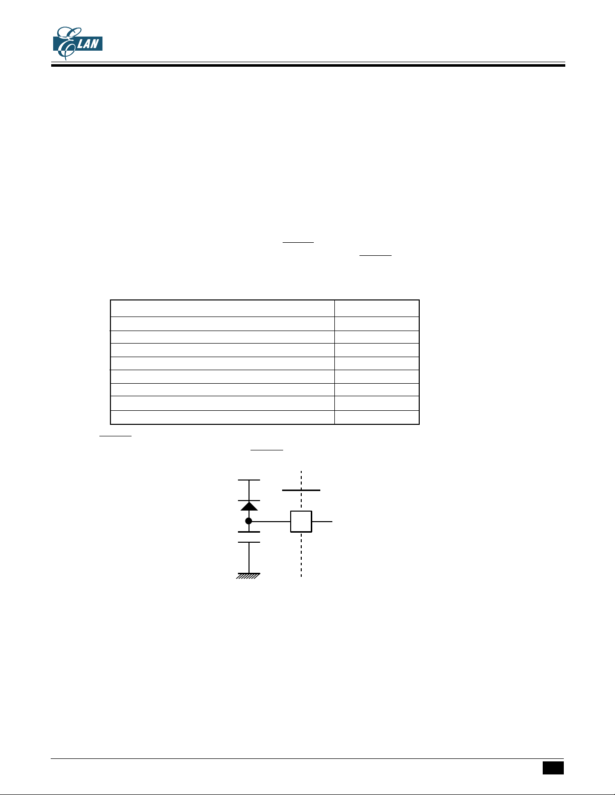
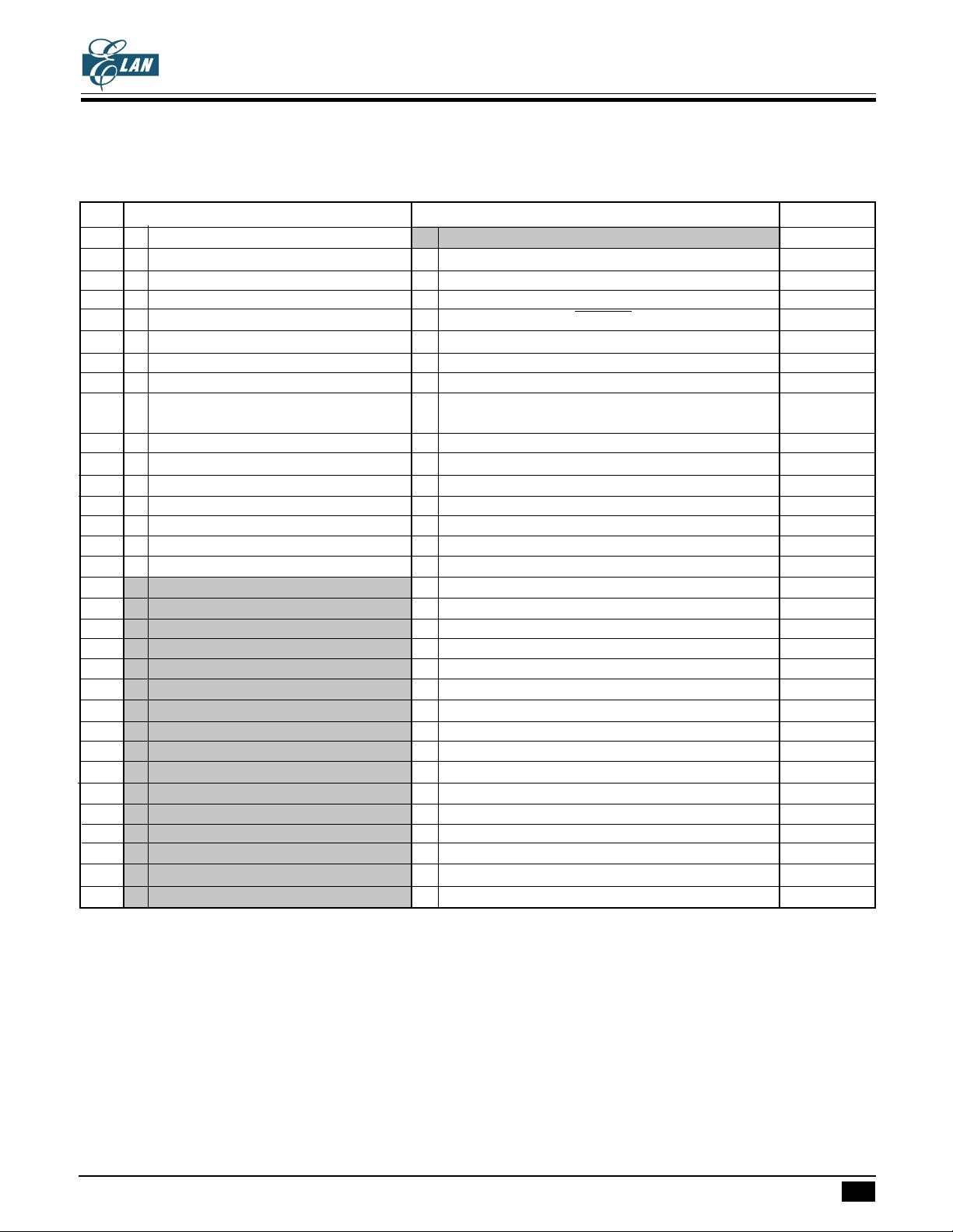
The RESET pin is a hysteresis input pin and it has a pull-up resistor available by mask option.
The simplest RESET circuit is connect RESET pin with a capacitor to V
and a diode to VDD.
SS
RESET
* This specification are subject to be changed without notice.
6.14.2001
25
Page 26
EM73963A
4-BIT MICRO-CONTROLLER FOR LCD PRODUCT
EM73963A I/O PORT DESCRIPTION :
Port Input function Output function Note
0 E Input port , wakeup function
1-- -2-- -3 -- I P3(0..2) : ROM bank selection
4 E Input port E Output port, P4.0/SOUND
5-- -6-- -7-- -8 E Input port, wakeup function, E Output port
external interrupt input
9 -- I P9.3 : RAM bank selection
10 -- -11 -- -12 -- -13 -- -14 I CPU status register -15 -- -16 I STOP mode control register
17 I Sound effect volume control register
18 -19 I IDLE mode control register
20 -21 -22 I DUAL/SLOW mode control register
23 I Sound effect frequency register low nibble
24 I Sound effect frequency register high nibble
25 I Timebase control register
26 I LCD common start address register
27 I LCD control register
28 I Timer/counter A control register
29 I Timer/counter B control register
30 I Sound effect command register
31 --
* This specification are subject to be changed without notice.
6.14.2001
26
Page 27
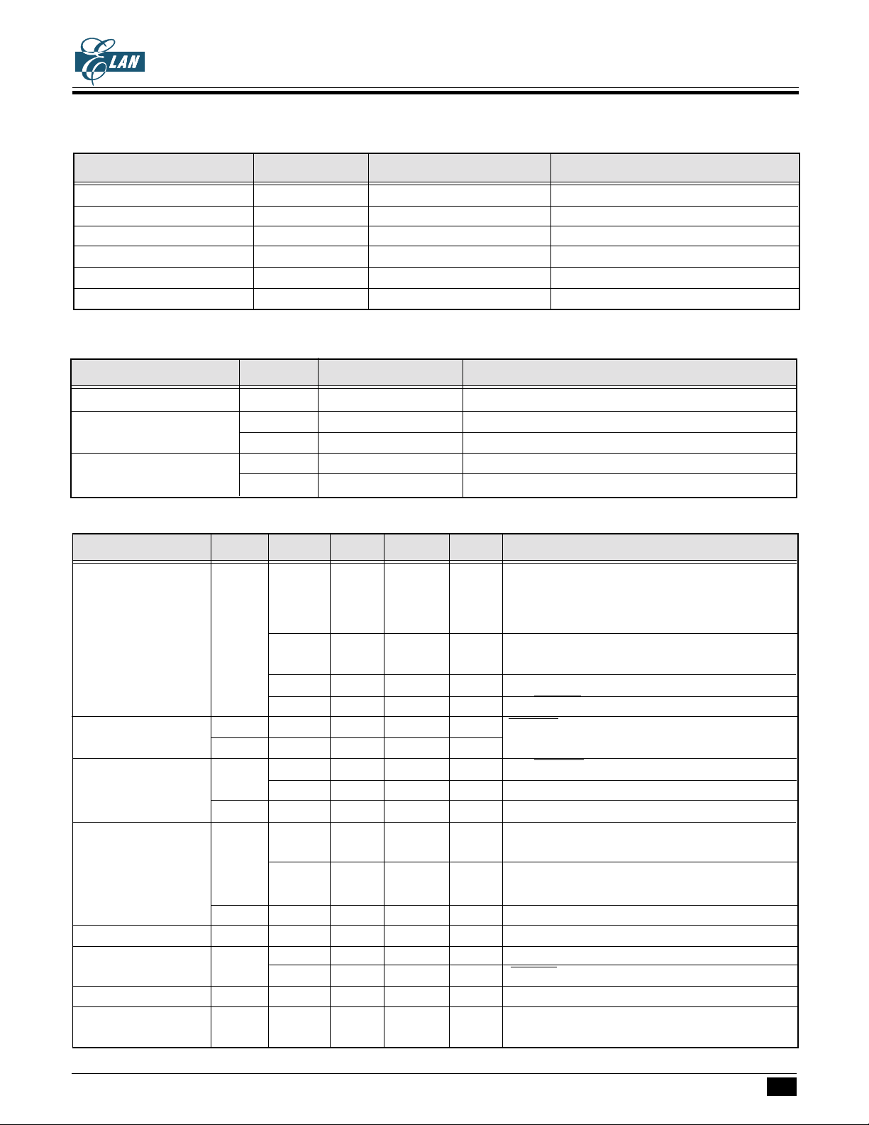
ABSOLUTE MAXIMUM RATINGS
Items Sym. Ratings Conditions
EM73963A
4-BIT MICRO-CONTROLLER FOR LCD PRODUCT
Supply Voltage V
Input Voltage V
Output Voltage V
Power Dissipation P
Operating Temperature T
Storage Temperature T
DD
IN
O
D
OPR
STG
-0.5V to 6V
-0.5V to VDD+0.5V
-0.5V to VDD+0.5V
300mW T
0oC to 50oC
-55oC to 125oC
OPR
=50oC
RECOMMANDED OPERATING CONDITIONS
Items Sym. Ratings Condition
Supply Voltage V
Input Voltage V
Operating Frequency F
DD
IH
V
IL
C
Fs 32KHz LXIN,LXOUT (crystal/RC osc)
DC ELECTRICAL CHARACTERISTICS (VDD=3±0.3V, VSS=0V, T
2.4V to 5.5V
0.90xVDD to V
0V to 0.10xV
DD
DD
480K to 4MHz CLK (RC osc)
OPR
=25oC)
Parameters Sym. Min. Typ. Max. Unit Conditions
Supply current I
Hysteresis voltage V
Input current I
Output voltage V
Leakage current I
Input resistor R
V
I
V
DD
HYS+
HYS-
IH
IL
OH
OL
LO
IN
Frequency stability - 15 - % Fc=4MHz, RC osc, [F(3V)-F(2.4V)]/F(3V)
Frequency variation - 20 - % Fc=4MHz, V
-0.9 2mAV
=3.3V, no load, NORMAL mode,
DD
Fs=32KHz (R=750kΩ),
Fc=4MHz (RC osc : R=5.6KΩ, C=20pF)
-1225µAV
=3.3V, no load, SLOW mode, Fs=32KHz
DD
LCD on
-410µAV
-0.1 1µAV
0.50V
0.20V
DD
DD
- 0.75V
- 0.40V
V RESET, P0, P8
DD
V
DD
=3.3V, IDLE mode, LCD off
DD
=3.3V, STOP mode
DD
- - ±1 µA P0, RESET, VDD=3.3V, VIH=3.3/0V
- - ±1 µA Open-drain, V
=3.3V, VIH=3.3/0V
DD
- -250 -500 µA Push-pull, VDD=3.3V, VIL=0.4V, except P4
2.4 - - V Push-pull, P4(high current PMOS), SOUND,
V
=2.7V, IOH=-0.9mA
DD
2.0 2.4 - V Push-pull, P4(low current PMOS), P8,
V
=2.7V, IOH=-40µA
DD
- 0.15 0.3 V VDD=2.7V, IOL=0.9mA
- - 1 µA Open-drain, VDD=3.3V, VO=3.3V
80 150 230 K Ω P0
200 400 600 K Ω RESET
=3V,RC osc,
DD
[F(typical)-F(worse case)]/F(typical)
* This specification are subject to be changed without notice.
6.14.2001
27
Page 28
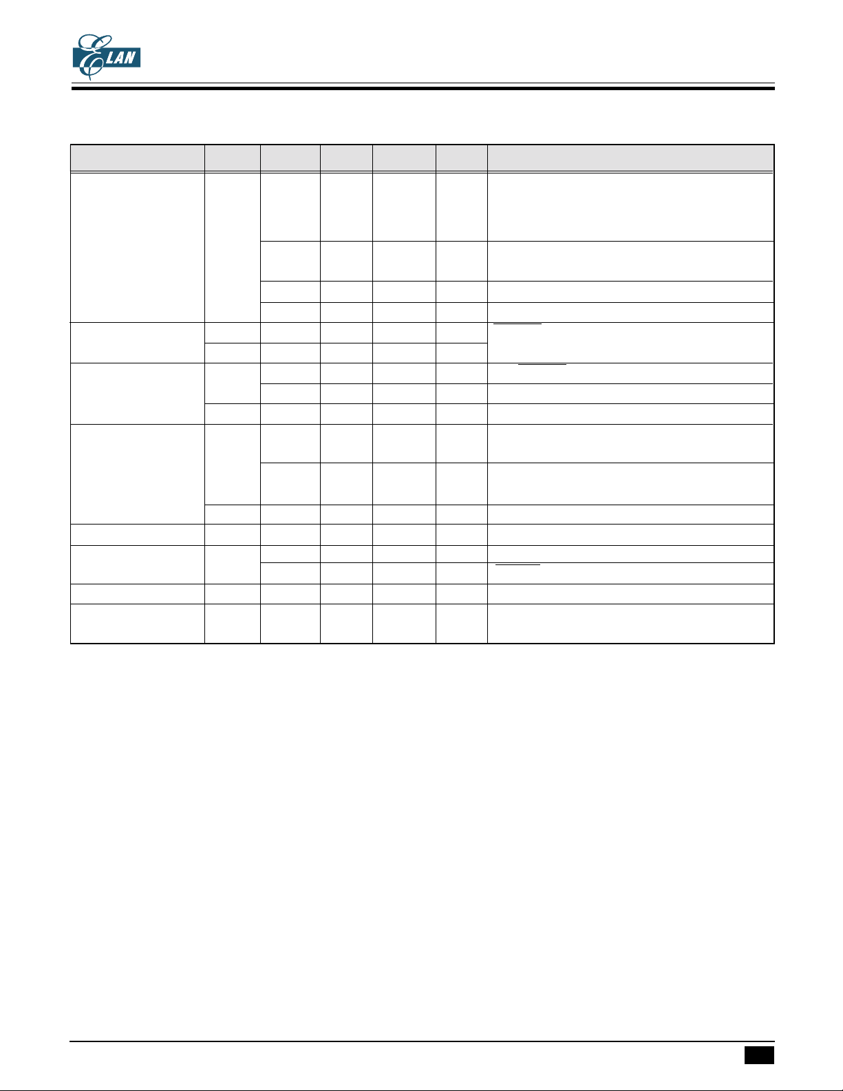
EM73963A
4-BIT MICRO-CONTROLLER FOR LCD PRODUCT
(VDD=4.5±0.5V, VSS=0V, T
OPR
=25oC)
Parameters Sym. Min. Typ. Max. Unit Conditions
Supply current I
Hysteresis voltage V
Input current I
Output voltage V
Leakage current I
Input resistor R
V
I
V
DD
HYS+
HYS-
IH
IL
OH
OL
LO
IN
Frequency stability - 15 - % Fc=4MHz,RC osc,[F(4.5V)-F(3.6V)]/F(4.5V)
Frequency variation - 20 - % Fc=4MHz, V
-1.5 2mAV
=5.0V, no load, NORMAL mode,
DD
Fs=32KHz (R=820kΩ),
Fc=4MHz (RC osc : R=5.6KΩ, C=20pF)
-3565µAV
=5.0V, no load, SLOW mode, Fs=32KHz
DD
LCD on
-815µAV
-0.1 1µAV
0.50V
0.20V
DD
DD
- 0.75V
- 0.40V
V RESET, P0, P8
DD
V
DD
=5.0V, IDLE mode, LCD off
DD
=5.0V, STOP mode
DD
- - ±1 µA P0, RESET, VDD=5.0V, VIH=5.0/0V
- - ±1 µA Open-drain, VDD=5.0V, VIH=5.0/0V
- - -1 mA Push-pull, VDD=5.0V, VIL=0.4V, except P4
3.0 - - V Push-pull, P4(high current PMOS), SOUND,
V
=4.0V, IOH=-4mA
DD
2.4 - - V Push-pull, P4(low current PMOS), P8,
V
=4.0V, IOH=-200µA
DD
-- 1VV
=4.0V, IOL=4mA
DD
- - 1 µA Open-drain, VDD=5.0V, VO=5.0V
40 75 120 K Ω P0
100 200 300 KΩ RESET
=4.5V,RC osc,
DD
[F(typical)-F(worse case)]/F(typical)
* This specification are subject to be changed without notice.
6.14.2001
28
Page 29
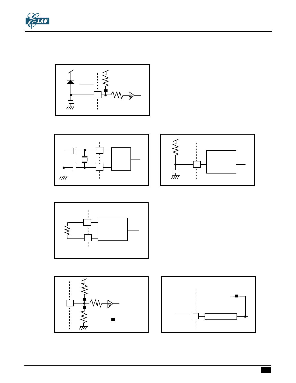
RESET PIN TYPE
TYPE RESET-A
EM73963A
4-BIT MICRO-CONTROLLER FOR LCD PRODUCT
RESET
OSCILLATION PIN TYPE
TYPE OSC-B TYPE OSC-C
LXIN
LXOUT
TYPE OSC-F
LXIN
mask option
Crystal
Osc.
RC Osc.
(inverter)
CLK
RC Osc.
(comparator)
LXOUT
INPUT PIN TYPE
TYPE INPUT-A TYPE INPUT-B
: mask option
* This specification are subject to be changed without notice.
WAKEUP function
mask option
P0/WAKEUP TYPE INPUT-A
6.14.2001
29
Page 30
4-BIT MICRO-CONTROLLER FOR LCD PRODUCT
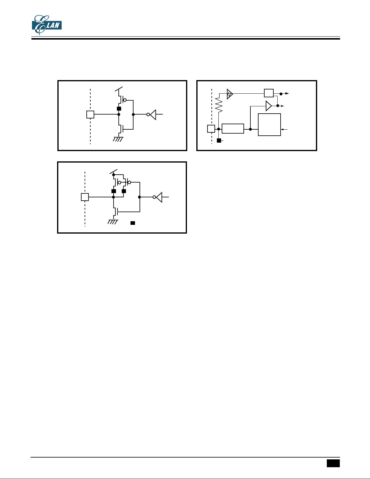
I/O PIN TYPE
TYPE I/O TYPE I/O-L
mask option
TYPE I/O
WAKEUP function
mask option
TYPE I/O-O
path B
path A
SEL
Output
data
latch
EM73963A
Special function
control input
Input
data
Output
data
: mask option
Path A : For set and clear bit of port instructions, data goes through path A from output data latch to CPU.
Path B : For input and test instructions, data from output pin go through path B to CPU and the output data latch
will be set to high.
* This specification are subject to be changed without notice.
6.14.2001
30
Page 31
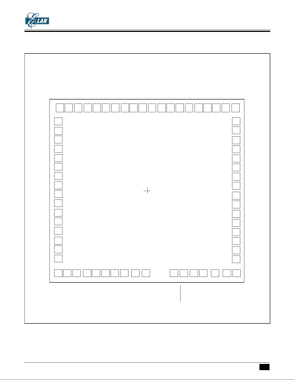
PAD DIAGRAM
SEG23
69 68 67 66 65 64 63 62 61 60 56 55 5459 58 57 53 52 51 50
SEG22
SEG21
SEG20
SEG19
SEG18
SEG17
EM73963A
4-BIT MICRO-CONTROLLER FOR LCD PRODUCT
SEG16V4V3
V2
V1
SEG14
SEG15
SEG13
SEG12
SEG11
SEG10
SEG9
SEG8
SEG24
SEG25
SEG26
SEG27
SEG28
SEG29
SEG30
SEG31
SEG32
SEG33
SEG34
SEG35
SEG36
SEG37
SEG38
SEG39
10
11
12
13
14
15
16
1
2
3
4
5
6
7
8
9
EM73963A
(0,0)
37
36
ELAN
49
48
47
46
45
44
43
42
41
40
39
38
35
34
SEG7
SEG6
SEG5
SEG4
SEG3
SEG2
SEG1
SEG0
COM7
COM6
COM5
COM4
COM3
COM2
COM1
COM0
17 18 19 20 21 22 23 24 25 26 27 28 29 30 31 32 33
P8.3
P8.2
P8.1
P8.0
P0.3
P0.2
P0.1
P0.0
VSS
LXIN
* This specification are subject to be changed without notice.
RESET
LXOUT
CLK
TEST
VDD
P4.0
SOUND
6.14.2001
31
Page 32
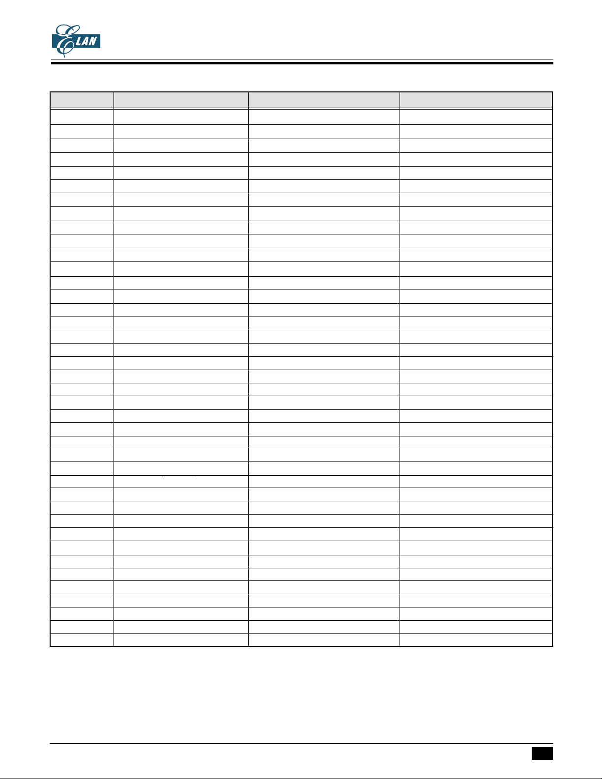
4-BIT MICRO-CONTROLLER FOR LCD PRODUCT
Pad No. Symbol X Y
1 SEG24 -1153.5 903.0
2 SEG25 -1153.5 783.1
3 SEG26 -1153.5 663.2
4 SEG27 -1153.5 543.3
5 SEG28 -1153.5 423.4
6 SEG29 -1153.5 303.5
7 SEG30 -1153.5 183.6
8 SEG31 -1153.5 63.7
9 SEG32 -1153.5 -56.2
10 SEG33 -1153.5 -176.1
11 SEG34 -1153.5 -296.0
12 SEG35 -1153.5 -415.9
13 SEG36 -1153.5 -535.8
14 SEG37 -1153.5 -655.7
15 SEG38 -1153.5 -775.6
16 SEG39 -1153.5 -895.5
17 P8.3 -1157.6 -1077.5
18 P8.2 -1036.1 -1077.5
19 P8.1 -914.4 -1077.5
20 P8.0 -794.8 -1077.5
21 P0.3 -671.8 -1077.5
22 P0.2 -551.9 -1077.5
23 P0.1 -428.9 -1077.5
24 P0.0 -309.0 -1077.5
25 VSS -161.3 -1077.5
26 LXIN -17.8 -1077.5
27 LXOUT 354.3 -1077.5
28 RESET 480.9 -1077.5
29 CLK 600.8 -1077.5
30 TEST 722.8 -1077.5
31 VDD 879.4 -1077.5
32 P4.0 1035.0 -1077.5
33 SOUND 1158.1 -1077.5
34 COM0 1151.3 -895.5
35 COM1 1151.3 -775.6
36 COM2 1151.3 -655.7
37 COM3 1151.3 -535.8
38 COM4 1151.3 -415.9
39 COM5 1151.3 -296.0
40 COM6 1151.3 -176.1
EM73963A
* This specification are subject to be changed without notice.
6.14.2001
32
Page 33
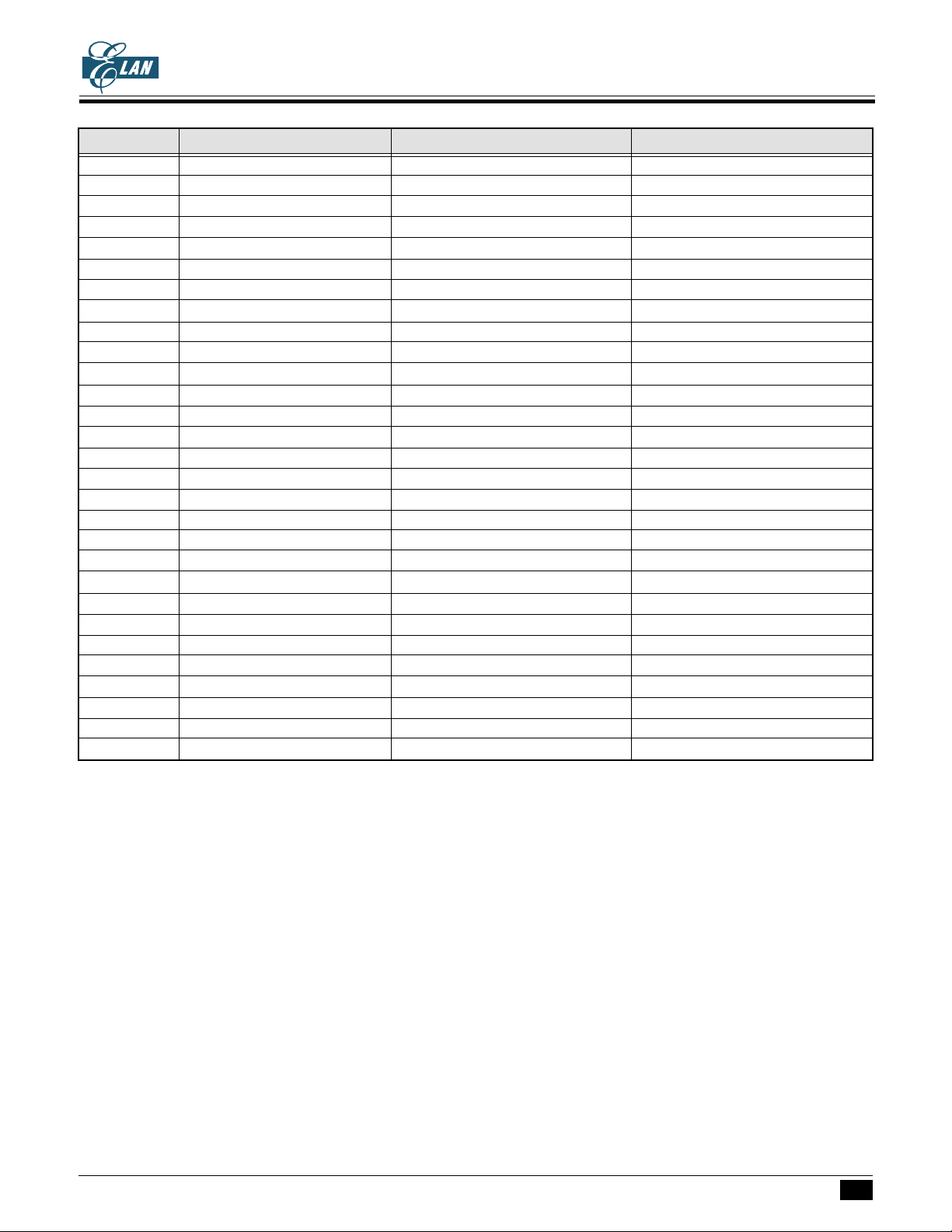
4-BIT MICRO-CONTROLLER FOR LCD PRODUCT
Pad No. Symbol X Y
41 COM7 1151.3 -56.2
42 SEG0 1151.3 63.7
43 SEG1 1151.3 183.6
44 SEG2 1151.3 303.5
45 SEG3 1151.3 423.4
46 SEG4 1151.3 543.3
47 SEG5 1151.3 663.2
48 SEG6 1151.3 783.1
49 SEG7 1151.3 903.0
50 SEG8 1138.1 1077.8
51 SEG9 1018.2 1077.8
52 SEG10 898.3 1077.8
53 SEG11 778.4 1077.8
54 SEG12 658.5 1077.8
55 SEG13 538.6 1077.8
56 SEG14 418.7 1077.8
57 SEG15 298.8 1077.8
58 V1 178.9 1077.8
59 V2 59.0 1077.8
60 V3 -60.9 1077.8
61 V4 -180.8 1077.8
62 SEG16 -300.7 1077.8
63 SEG17 -420.6 1077.8
64 SEG18 -540.5 1077.8
65 SEG19 -660.4 1077.8
66 SEG20 -780.3 1077.8
67 SEG21 -900.2 1077.8
68 SEG22 -1020.1 1077.8
69 SEG23 -1140.0 1077.8
EM73963A
Chip Size : 2620 x 2470 µm
Unit : µm
For PCB layout, IC substrate must be floated or connected to VSS.
* This specification are subject to be changed without notice.
6.14.2001
33
Page 34
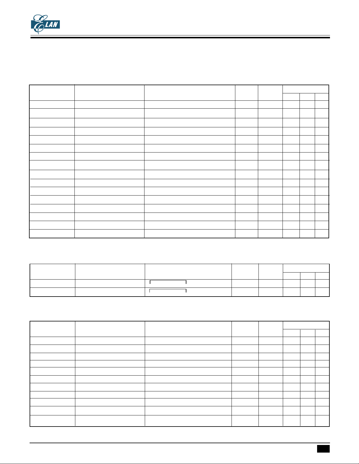
EM73963A
4-BIT MICRO-CONTROLLER FOR LCD PRODUCT
INSTRUCTION TABLE
(1) Data Transfer
Mnemonic Object code ( binary ) Operation description Byte Cycle Flag
CZ S
LDA x 0110 1010 xxxx xxxx Acc←RAM[x] 2 2 - Z 1
LDAM 0101 1010 Acc ←RAM[HL] 1 1 - Z 1
LDAX 0110 0101 Acc←ROM[DP]
LDAXI 0110 0111 Acc←ROM[DP]
L
,DP+1 1 2 - Z 1
H
LDH #k 1001 kkkk HR←k11--1
LDHL x 0100 1110 xxxx xx00 LR←RAM[x],HR←RAM[x+1] 2 2 - - 1
LDIA #k 1101 kkkk Acc←k11-Z1
LDL #k 1000 kkkk LR←k11--1
STA x 0110 1001 xxxx xxxx RAM[x]←Acc 2 2 - - 1
STAM 0101 1001 RAM[HL]←Acc 1 1 - - 1
STAMD 0111 1101 RAM[HL]←Acc, LR-1 1 1 - Z C
STAMI 0111 1111 RAM[HL]←Acc, LR+1 1 1 - Z C'
STD #k,y 0100 1000 kkkk yyyy RAM[y]←k22--1
STDMI #k 1010 kkkk RAM[HL]←k, LR+1 1 1 - Z C'
THA 0111 0110 Acc←HR 1 1 - Z 1
TLA 0111 0100 Acc←LR 1 1 - Z 1
12-Z1
(2) Rotate
Mnemonic Object code ( binary ) Operation description Byte Cycle Flag
CZS
RLCA 0101 0000 ←CF←Acc← 11CZC'
RRCA 0101 0001 →CF→Acc→ 11CZC'
(3) Arithmetic operation
Mnemonic Object code ( binary ) Operation description Byte Cycle Flag
C ZS
ADCAM 0111 0000 Acc←Acc + RAM[HL] + CF 1 1 C Z C'
ADD #k,y 0100 1001 kkkk yyyy RAM[y]←RAM[y] +k 2 2 - Z C'
ADDA #k 0110 1110 0101 kkkk Acc←Acc+k 2 2 - Z C'
ADDAM 0111 0001 Acc←Acc + RAM[HL] 1 1 - Z C'
ADDH #k 0110 1110 1001 kkkk HR←HR+k 2 2 - Z C'
ADDL #k 0110 1110 0001 kkkk LR←LR+k 2 2 - Z C'
ADDM #k 0110 1110 1101 kkkk RAM[HL]←RAM[HL] +k 2 2 - Z C'
DECA 0101 1100 Acc←Acc-1 1 1 - Z C
DECL 0111 1100 LR←LR-1 1 1 - Z C
DECM 0101 1101 RAM[HL]←RAM[HL] -1 1 1 - Z C
INCA 0101 1110 Acc←Acc + 1 1 1 - Z C'
* This specification are subject to be changed without notice.
6.14.2001
34
Page 35
EM73963A
4-BIT MICRO-CONTROLLER FOR LCD PRODUCT
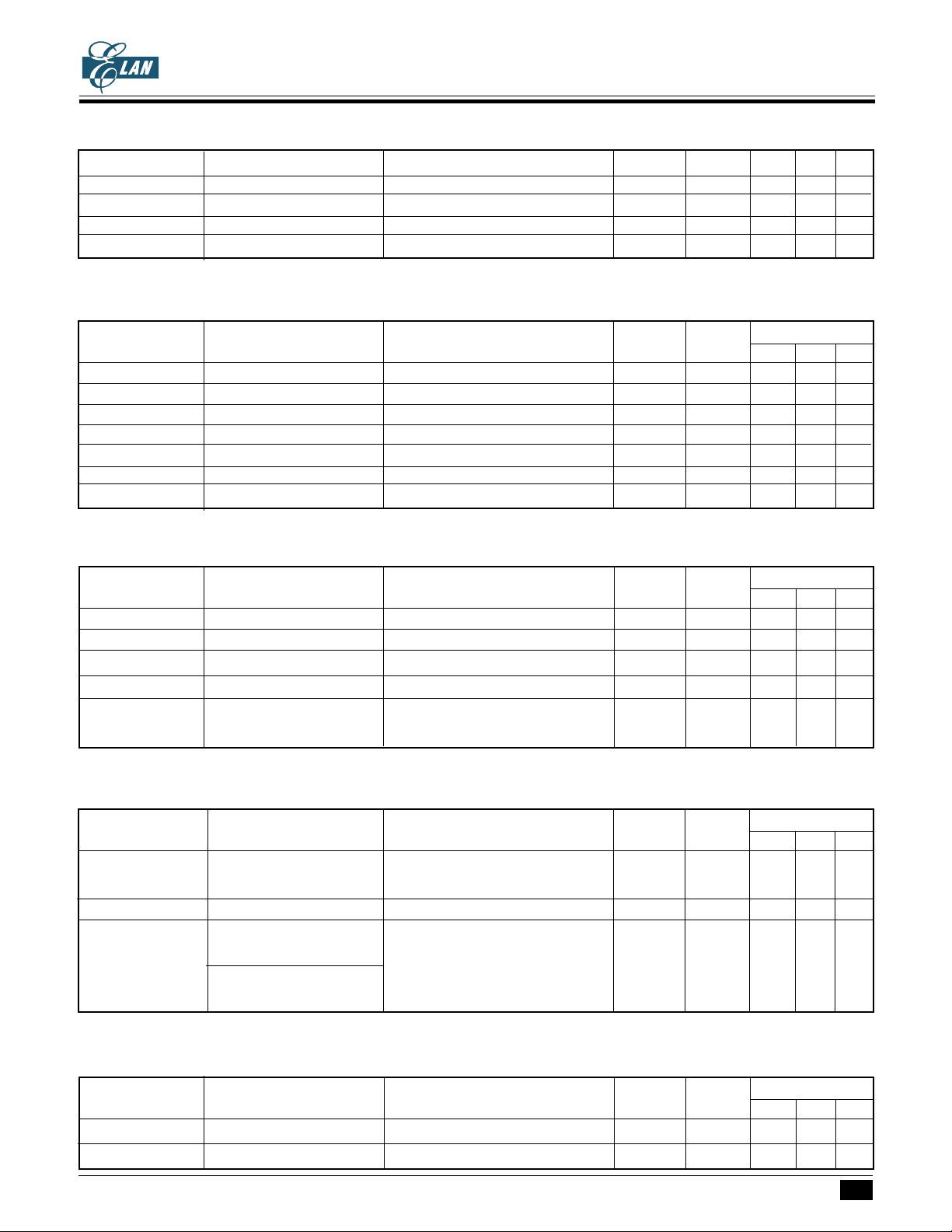
INCL 0111 1110 LR←LR + 1 1 1 - Z C'
INCM 0101 1111 RAM[HL]←RAM[HL]+1 1 1 - Z C'
SUBA #k 0110 1110 0111 kkkk Acc←k-Acc 2 2 - Z C
SBCAM 0111 0010 Acc←RAM[HLl - Acc - CF' 1 1 C Z C
SUBM #k 0110 1110 1111 kkkk RAM[HL]←k - RAM[HL] 2 2 - Z C
(4) Logical operation
Mnemonic Object code ( binary ) Operation description Byte Cycle Flag
CZS
ANDA #k 0110 1110 0110 kkkk Acc←Acc&k 2 2 - Z Z'
ANDAM 0111 1011 Acc←Acc & RAM[HL] 1 1 - Z Z'
ANDM #k 0110 1110 1110 kkkk RAM[HL]←RAM[HL]&k 2 2 - Z Z'
ORA #k 0110 1110 0100 kkkk Acc←Acc k 2 2 - Z Z'
ORAM 0111 1000 Acc ←Acc RAM[HL] 1 1 - Z Z'
ORM #k 0110 1110 1100 kkkk RAM[HL]←RAM[HL] k 2 2 - Z Z'
XORAM 0111 1001 Acc←Acc^RAM[HL] 1 1 - Z Z'
- -
- -
- -
(5) Exchange
Mnemonic Object code ( binary ) Operation description Byte Cycle Flag
CZS
EXA x 0110 1000 xxxx xxxx Acc↔RAM[x] 2 2 - Z 1
EXAH 0110 0110 Acc↔HR 1 2 - Z 1
EXAL 0110 0100 Acc↔LR 1 2 - Z 1
EXAM 0101 1000 Acc↔RAM[HL] 1 1 - Z 1
EXHL x 0100 1100 xxxx xx00 LR↔RAM[x],
HR↔RAM[x+1] 2 2 - - 1
(6) Branch
Mnemonic Object code ( binary ) Operation description Byte Cycle Flag
CZS
SBR a 00aa aaaa If SF=1 then PC←PC
12-6.a5-0
11--1
else null
LBR a 1100 aaaa aaaa aaaa If SF= 1 then PC←a else null 2 2 - - 1
SLBR a 0101 0101 1100 aaaa If SF=1 then PC←a else null 3 3 - - 1
aaaa aaaa (a:1000~1FFFh)
0101 0111 1100 aaaa
aaaa aaaa (a:0000~0FFFh)
(7) Compare
Mnemonic Object code ( binary ) Operation description Byte Cycle Flag
CZS
CMP #k,y 0100 1011 kkkk yyyy k-RAM[y] 2 2 C Z Z'
CMPA x 0110 1011 xxxx xxxx RAM[x]-Acc 2 2 C Z Z'
* This specification are subject to be changed without notice.
6.14.2001
35
Page 36
EM73963A
4-BIT MICRO-CONTROLLER FOR LCD PRODUCT
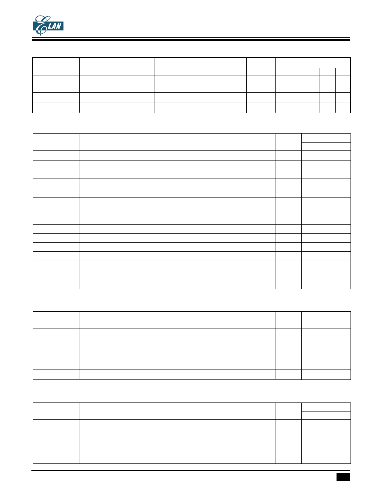
Mnemonic Object code ( binary ) Operation description Byte Cycle Flag
CZS
CMPAM 0111 0011 RAM[HL] - Acc 1 1 C Z Z'
CMPH #k 0110 1110 1011 kkkk k - HR 2 2 - Z C
CMPIA #k 1011 kkkk k - Acc 1 1 C Z Z'
CMPL #k 0110 1110 0011 kkkk k-LR 2 2 - Z C
(8) Bit manipulation
Mnemonic Object code ( binary ) Operation description Byte Cycle Flag
CZS
CLM b 1111 00bb RAM[HL]
CLP p,b 0110 1101 11bb pppp PORT[p]
CLPL 0110 0000 PORT[LR
CLR y,b 0110 1100 11bb yyyy RAM[y]
SEM b 1111 01bb RAM[HL]
SEP p,b 0110 1101 01bb pppp PORT[p]
SEPL 0110 0010 PORT[LR
SET y,b 0110 1100 01bb yyyy RAM[y]
TF y,b 0110 1100 00bb yyyy SF←RAM[y]
TFA b 1111 10bb SF←Acc
TFM b 1111 11bb SF←RAM[HL]
TFP p,b 0110 1101 00bb pppp SF←PORT[p]
TFPL 0110 0001 SF←PORT[LR
TT y,b 0110 1100 10bb yyyy SF←RAM[y]
TTP p,b 0110 1101 10bb pppp SF←PORT[p]
←011--1
b
←022--1
b
+4]LR
3-2
←022--1
b
←111--1
b
←122--1
b
+4]LR
3-2
←122--1
b
'11--*
b
←012--1
1-0
←112 --1
l-0
'22--*
b
'11--*
b
'22--*
b
b
b
+4]LR
3-2
'1 2--*
1-0
22--*
22--*
(9) Subroutine
Mnemonic Object code ( binary ) Operation description Byte Cycle Flag
CZS
LCALL a 0100 0aaa aaaa aaaa STACK[SP]←PC, 2 2 - - -
SP←SP -1, PC←a
SCALL a 1110 nnnn STACK[SP]←PC, 1 2 - - -
SP←SP - 1, PC←a, a = 8n + 6
(n =1∼15),0086h (n = 0)
RET 0100 1111 SP←SP + 1, PC←STACK[SP] 1 2 - - -
(10) Input/output
Mnemonic Object code ( binary ) Operation description Byte Cycle Flag
CZS
INA p 0110 1111 0100 pppp Acc←PORT[p] 2 2 - Z Z'
INM p 0110 1111 1100 pppp RAM[HL]←PORT[p] 2 2 - - Z'
OUT #k,p 0100 1010 kkkk pppp PORT[p]←k22--1
OUTA p 0110 1111 000p pppp PORT[p]←Acc 2 2 - - 1
OUTM p 0110 1111 100p pppp PORT[p]←RAM[HL] 2 2 - - 1
* This specification are subject to be changed without notice.
6.14.2001
36
Page 37
EM73963A
4-BIT MICRO-CONTROLLER FOR LCD PRODUCT
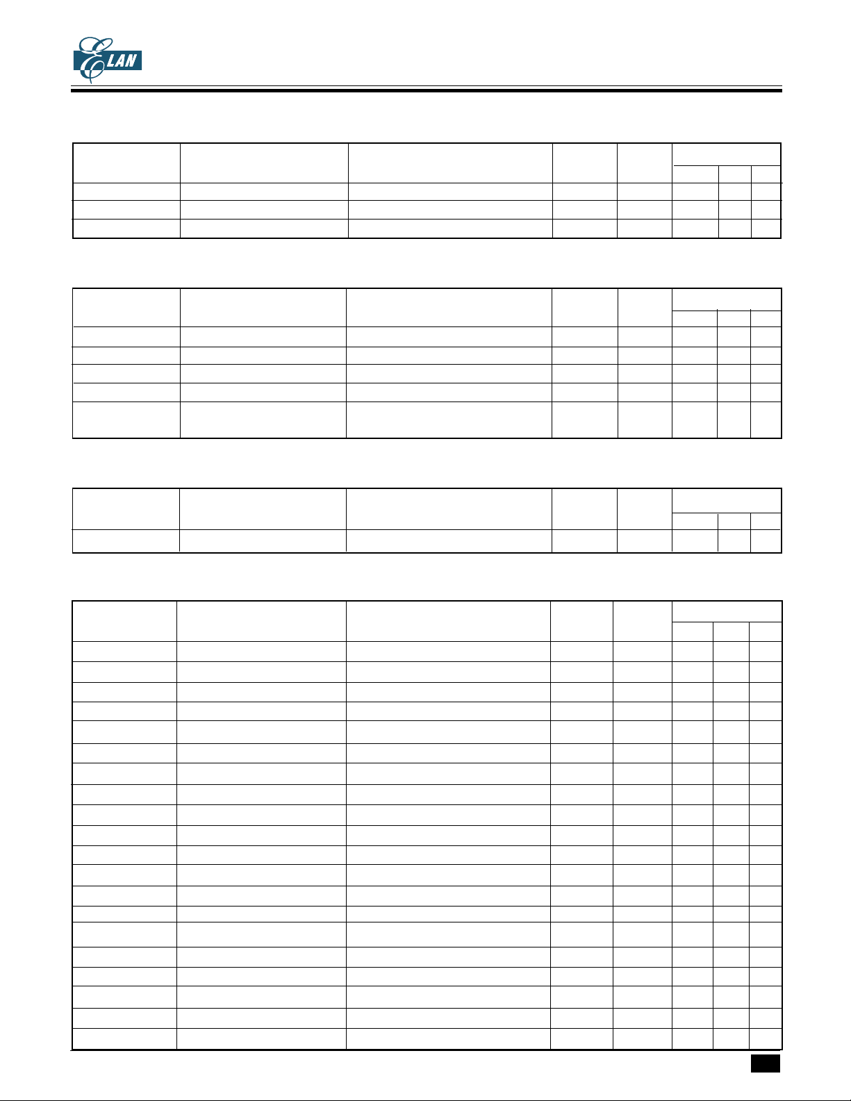
(11) Flag manipulation
Mnemonic Object code ( binary ) Operation description Byte Cycle Flag
CZS
TFCFC 0101 0011 SF←CF', CF←0110-*
TTCFS 0101 0010 SF←CF, CF←1111-*
TZS 0101 1011 SF←ZF 1 1 - - *
(12) Interrupt control
Mnemonic Object code ( binary ) Operation description Byte Cycle Flag
CZS
CIL r 0110 0011 11rr rrrr IL←IL & r 2 2 - - 1
DICIL r 0110 0011 10rr rrrr EIF←0,IL←IL&r 2 2 - - 1
EICIL r 0110 0011 01rr rrrr EIF←1,IL←IL&r 2 2 - - 1
EXAE 0111 0101 MASK↔Acc 1 1 - - 1
RTI 0100 1101 SP←SP+1,FLAG.PC 1 2 * * *
←STACK[SP],EIF ←1
(13) CPU control
Mnemonic Object code ( binary ) Operation description Byte Cycle Flag
CZS
NOP 0101 0110 no operation 1 1 - - -
(14) Timer/Counter & Data pointer & Stack pointer control
Mnemonic Object code ( binary ) Operation description Byte Cycle Flag
CZS
LDADPL 0110 1010 1111 1100 Acc←[DP]
LDADPM 0110 1010 1111 1101 Acc←[DP]
LDADPH 0110 1010 1111 1110 Acc←[DP]
L
M
H
22-Z1
22-Z1
22-Z1
LDASP 0110 1010 1111 1111 Acc←SP 2 2 - Z 1
LDATAL 0110 1010 1111 0100 Acc←[TA]
LDATAM 0110 1010 1111 0101 Acc←[TA]
LDATAH 0110 1010 1111 0110 Acc←[TA]
LDATBL 0110 1010 1111 1000 Acc←[TB]
LDATBM 0110 1010 1111 1001 Acc←[TB]
LDATBH 0110 1010 1111 1010 Acc←[TB]
STADPL 0110 1001 1111 1100 [DP]
STADPM 0110 1001 1111 1101 [DP]
STADPH 0110 1001 1111 1110 [DP]
←Acc 2 2 - - 1
L
←Acc 2 2 - - 1
M
←Acc 2 2 - - 1
H
L
M
H
L
M
H
22-Z1
22-Z1
22 -Z1
22-Z1
22-Z1
22-Z1
STASP 0110 1001 1111 1111 SP←Acc 2 2 - - 1
STATAL 0110 1001 1111 0100 [TA]
STATAM 0110 1001 1111 0101 [TA]
STATAH 0110 1001 1111 0110 [TA]
STATBL 0110 1001 1111 1000 [ TB]
STATBM 0110 1001 1111 1001 [TB]
STATBH 0110 1001 1111 1010 [TB]
* This specification are subject to be changed without notice.
←Acc 2 2 - - 1
L
←Acc 2 2 - - 1
M
←Acc 2 2 - - 1
H
←Acc 2 2 - - 1
L
←Acc 2 2 - - 1
M
←Acc 2 2 - - 1
H
6.14.2001
37
Page 38
4-BIT MICRO-CONTROLLER FOR LCD PRODUCT
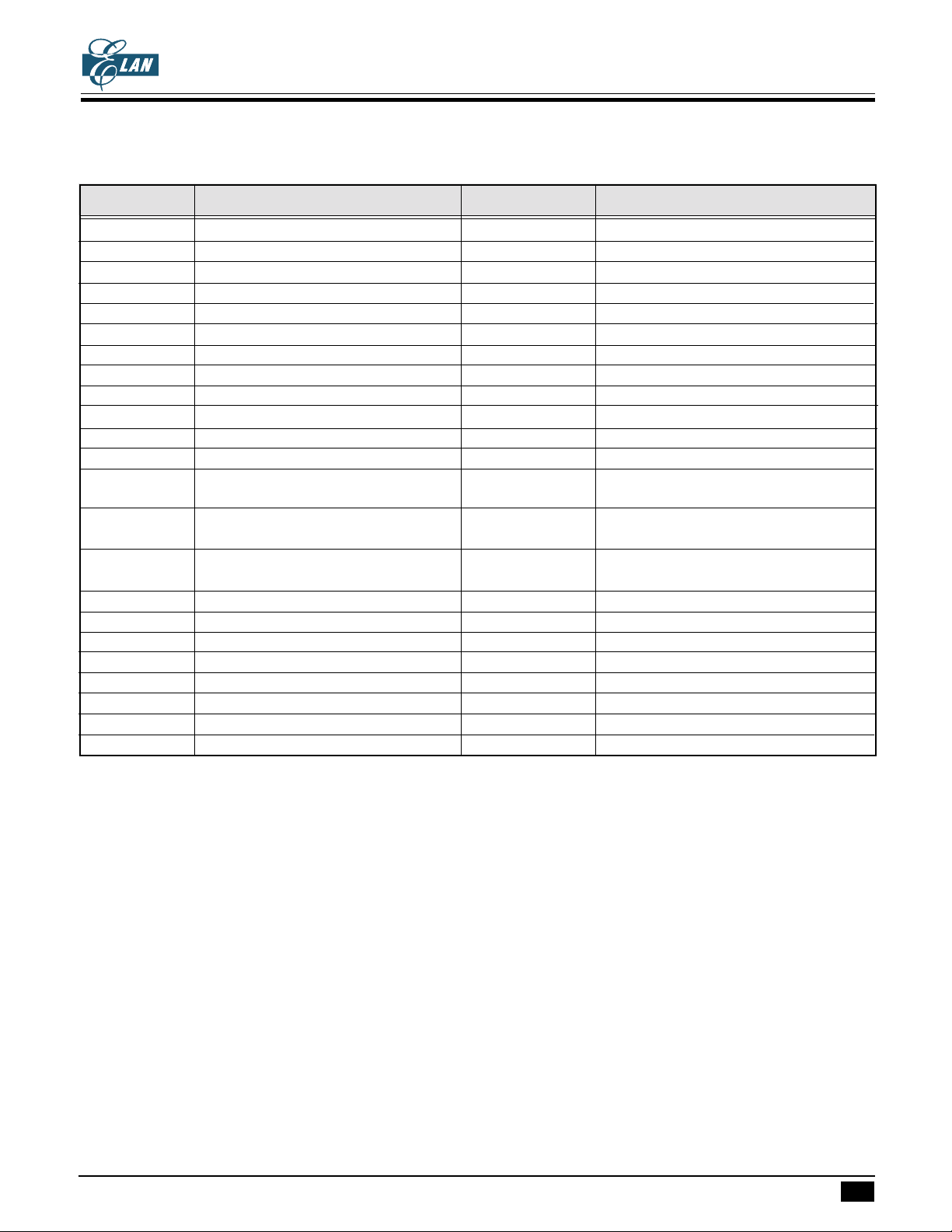
**** SYMBOL DESCRIPTION
Symbol Description Symbol Description
HR H register LR L register
PC Program counter DP Data pointer
SP Stack pointer STACK[SP] Stack specified by SP
A
CC
CF Carry flag ZF Zero flag
SF Status flag EI Enable interrupt register
IL Interrupt latch MASK Interrupt mask
PORT[p] Port ( address : p ) ΤΑ Timer/counter A
ΤΒ Timer/counter B RAM[HL] Data memory (address : HL )
RAM[x] Data memory (address : x ) ROM[DP]
ROM[DP]
[DP]
M
[TA]L([TB]L) Low 4-bit of timer/counter A [TA]M([TB]M) Middle 4-bit of timer/counter A
[TA]H([TB]H) High 4-bit of timer/counter A LR
LR
3-2
PC
12-6
↔ Exchange + Addition
- Substraction & Logic AND
- -
#k 4-bit immediate data x 8-bit RAM address
y 4-bit zero-page address p 4-bit or 5-bit port address
b Bit address r 6-bit interrupt latch
Accumulator FLAG All flags
Low 4-bit of program memory
Low 4-bit of data pointer register
High 4-bit of data pointer register
High 4-bit of program memory [DP]
H
Middle 4-bit of data pointer register [DP]
L
L
H
(timer/counter B) register (timer/counter B) register
1-0
Contents of bit assigned by bit
(timer/counter B) register 1 to 0 of LR
Bit 3 to 2 of LR a
5-0
Bit 5 to 0 of destination address for
branch instruction
Bit 12 to 6 of program counter ← Transfer
Logic OR ^ Logic XOR
Inverse operation . Concatenation
EM73963A
* This specification are subject to be changed without notice.
6.14.2001
38
 Loading...