

Page 1
EtronTech
EM639165
8Mega x 16bits SDRAM
Preliminary (Rev 1.0, 2/2001)
Features
•
Single 3.3 ± 0.3V power supply
•
Fast clock rate
-
PC133: 133 MHz (CL3)
-
PC100: 100 MHz (CL2)
•
Fully synchronous operation referenced to clock
rising edge
•
4-bank operation controlled by BA0, BA1 (Bank
Address)
•
Programmable Mode registers
- /CAS Latency: 2 or 3
- Burst Length: 1, 2, 4, 8 or full page
- Burst Type: interleaved or linear burst
•
Byte Control – DQML and DQMU
•
Random column access
•
Auto precharge / All banks precharge controlled
by A10
•
Auto and self-refresh
•
Self-refresh mode: standard and low power
•
4096 refresh cycles/64ms
•
Interface: LVTTL
•
54-pin 400 mil plastic TSOP II package
Pin Assignment (Top View)
VDD
DQ0
VDDQ
DQ1
DQ2
VSSQ
DQ3
DQ4
VDDQ
DQ5
DQ6
VSSQ
DQ7
VDD
DQML
/WE
/CAS
/RAS
/CS
BA0
BA1
A10(AP)
A0
A1
A2
A3
VDD
1
2
3
4
5
6
7
8
9
10
11
12
13
14
15
16
17
18
19
20
21
22
23
24
25
26
27
54
53
52
51
50
49
48
47
46
45
44
43
42
41
40
39
38
37
36
35
34
33
32
31
30
29
28
Ordering Information
VSS
DQ15
VSSQ
DQ14
DQ13
VDDQ
DQ12
DQ11
VSSQ
DQ10
DQ9
VDDQ
DQ8
VSS
NC
DQMU
CLK
CKE
NC
A11
A9
A8
A7
A6
A5
A4
VSS
Key Specifications
EM639165
Clock Cycle time (min., CL=2)
t
CK2
Clock Cycle time (min., CL=3)
t
CK3
Access time (max., CL=2)
t
AC2
Access time (max., CL=3)
t
AC3
Row Active time (max.)
t
RAS
Row Cycle time(min.)
t
RC
-
75/8
10/10 ns
7.5/8 ns
6/6 ns
5.4/6 ns
45/48 ns
67.5/70 ns
Overview
EM639165 is a high-speed Synchronous Dynamic
Random Access Memory (SDRAM), organized as 4
banks x 2,097,152 words x 16 bits. All inputs and
outputs are referenced to the rising edge of CLK.
It achieves very high-speed data rates up to
133MHz, and is suitable for main memories or graphic
memories in computer systems. For handheld device
application, we also provide a low power option, with
self-refresh current under 800 µA.
Part Number Speed
Grade
Self refresh
current (Max.)
EM639165TS-75 PC133/CL3 2 mA
EM639165TS-75L PC133/CL3
800 µA
EM639165TS-8 PC100/CL2 2 mA
EM639165TS-8L PC100/CL2
800 µA
Etron Technology, Inc.
No. 6, Technology Rd. V, Science-Based Industrial Park, Hsinchu, Taiwan 30077, R.O.C.
TEL: (886)-3-5782345 FAX: (886)-3-5778671
Etron Technology, Inc., reserves the right to make changes to its products and specifications without notice.
Page 2

BLOCK DIAGRAM
EM639165
DQ0-15
I/O Buffer
Memory Array
4096 x512x16
Cell Array
Bank #0
Mode
Register
Address Buffer
A0-11
BA0,1
Memory Array
4096 x512x16
Cell Array
Bank #1
Control Circuitry
Clock Buffer
CLK CKE
Memory Array
4096 x512x16
Cell Array
Bank #2
Control Signal Buffer
/CS /RAS
/CAS
Memory Array
4096 x512x16
Cell Array
Bank #3
/WE
DQM
Preliminary Rev 1.0 Feb. 2001
2
Page 3
PIN FUNCTION
EM639165
CLK Input
CKE Input
/CS Input
/RAS, /CAS, /WE Input
A0-11 Input
BA0,1 Input
Master Clock:
All other inputs are referenced to the rising edge of CLK
Clock Enable:
CKE controls internal clock.When CKE is low, internal clock for
the following cycle is ceased. CKE is also used to select
auto / self-refresh.
After self-refresh mode is started, CKE becomes asynchronous input.
Self-refresh is maintained as long as CKE is low.
Chip Select:
When /CS is high, any command means No Operation.
Combination of /RAS, /CAS, /WE defines basic commands.
A0-11 specify the Row / Column Address in conjunction with BA0,1.
The Row Address is specified by A0-11.
The Column Address is specified byA0-8.
A10 is also used to indicate precharge option. When A10 is high at a
read / write command, an auto precharge is performed. When A10 is
high at a precharge command, all banks are precharged.
Bank Address:
BA0,1 specifies one of four banks to which a command is applied.
BA0,1 must be set with ACT, PRE , READ , WRITE commands.
DQ0-15
DQMU/L
VDD,VSS
Input / Output
Input
Power Supply
VDDQ,VSSQ Power Supply
Data In and Data out are referenced to the rising edge of CLK.
Din Mask / Output Disable:
When DQM(U/L) is high in burst write, Din for the current cycle is
masked. When DQM(U/L) is high in burst read,
Dout is disabled at the next but one cycle.
Power Supply for the memory array and peripheral circuitry.
VDDQ and VSSQ are supplied to the Output Buffers only.
Preliminary Rev 1.0 Feb. 2001
3
Page 4
BASIC FUNCTIONS
The EM639165 provides basic functions, bank (row)
activate, burst read / write, bank (row) precharge, and auto
/ self refresh.
Each command is defined by control signals of /RAS, /CAS
and /WE at CLK rising edge. In addition to 3 signals, /CS
CLK
/CS Chip Select : L=select, H=deselect
/RAS Command
/CAS
/WE Command
CKE Refresh Option @ refresh command
A10 Precharge Option @ precharge or read/write command
Command
EM639165
,CKE and A10 are used as chip select, refresh opt ion, and
precharge option, respectively .
To know the detailed definition of commands, please see
the command truth table.
define basic command
Activate (ACT) [/RAS =L, /CAS =/WE =H]
ACT command activates a row in an idle bank indicated by BA.
Read (READ) [/RAS =H, /CAS =L, /WE =H]
READ command starts burst read from the active bank indicated by BA. First output
data appears after /CAS latency. When A10 =H at this command, the bank is deactivated after the burst read (auto-precharge, READA).
Write (WRITE) [/RAS =H, /CAS =/WE =L]
WRITE command starts burst write to the active bank indicated by BA. Total data
length to be written is set by burst length. When A10 =H at this command, the bank
is deactivated after the burst write (auto-precharge, WRITEA).
Precharge (PRE) [/RAS =L, /CAS =H, /WE =L]
PRE command deactivates the active bank indicated by BA. This command also
terminates burst read / write operation. When A10 =H at this command, all banks
are deactivated (precharge all, PREA ).
Auto-Refresh (REFA) [/RAS =/CAS =L, /WE =CKE =H]
REFA command starts auto-refresh cycle. Refresh address including bank address
are generated internally . After this command, the banks are precharged automatically.
Preliminary Rev 1.0 Feb. 2001
4
Page 5
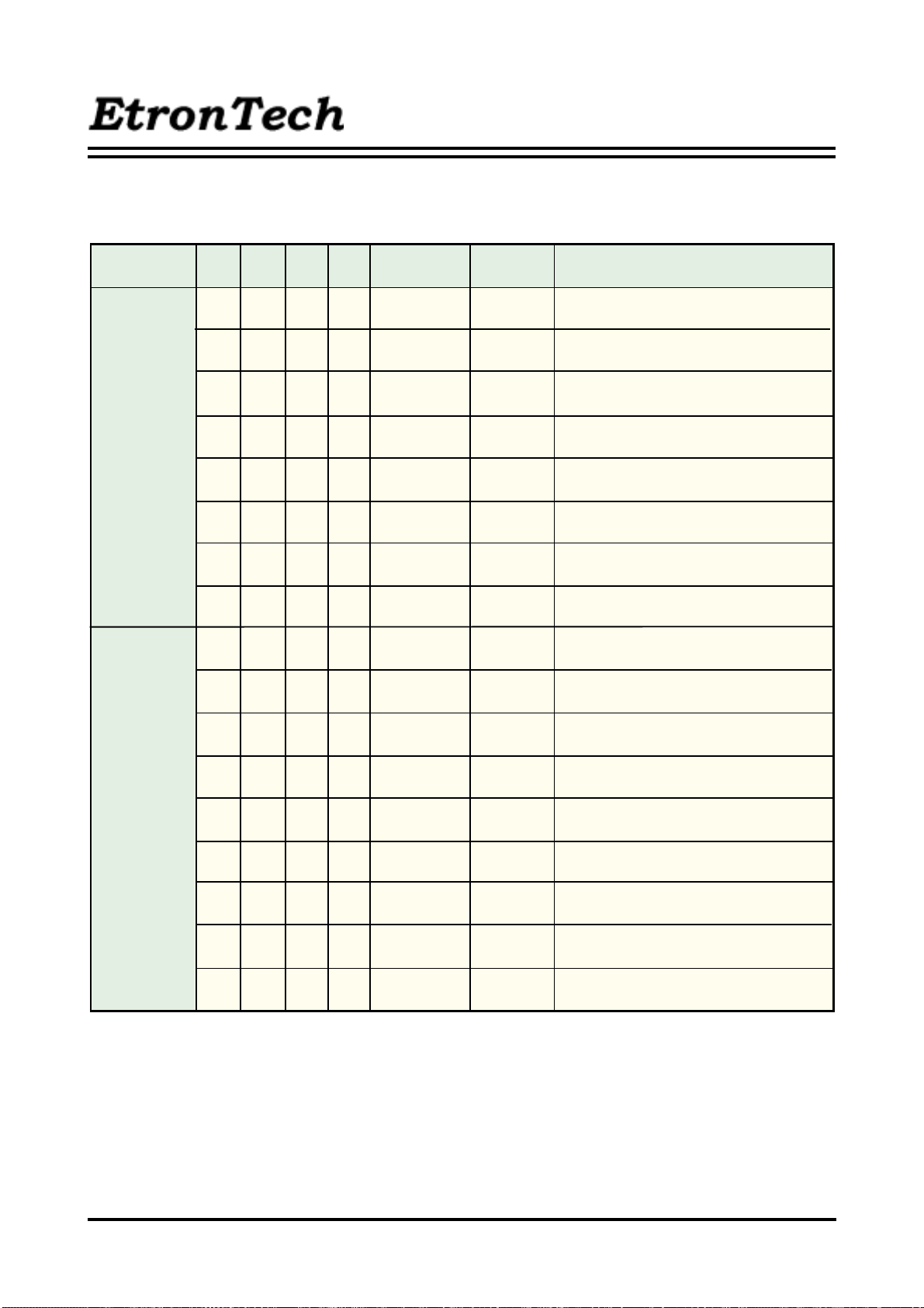
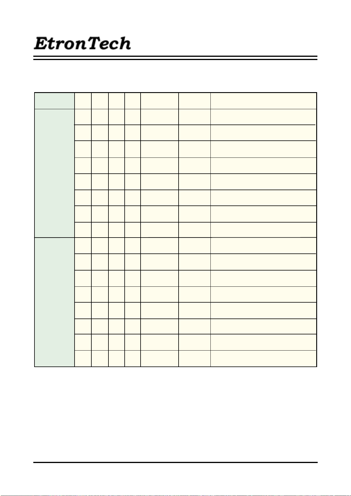
COMMAND TRUTH T ABLE
COMMAND
MNEMONIC
CKE
n-1
CKE
n
EM639165
/CS /RAS /CAS /WE BA0,1 A1 1 A10 A0-9
Deselect
No Operation
Row Address Entry &
Bank Active
Single Bank Precharge
Precharge All Banks
Column Address Entry
Column Address Entry &
Write with Auto-Precharge
Column Address Entry
Column Address Entry &
Read with Auto-Precharge
Auto-Refresh
Self-Refresh Entry
Self-Refresh Exit
&Write
& Read
DESEL HXHXXXX XXX
NOP HXLHHHXXXX
ACT
PRE
PREA
WRITE
WRITE A
READ
READA
REFA
REFS
REFSX
HXLL HHVVVV
HXLLHLVXLX
HXLLHL XHX
HXLHLLVVLV
HXLHLL VVHV
HXLHLHVVLV
HXLHLHVVHV
HHL L LHX XXX
HLL L LHX XXX
L HHXXXX XXX
L HLHHHX XXX
X
Burst Terminate
Mode Register Set
H=High Level, L=Low Level, V=Valid, X=Don't Care, n=CLK cycle number
NOTE: 1. A7-A9 =0, A0-A6 =Mode Address
Preliminary Rev 1.0 Feb. 2001
TBST HX L HHL XX XX
MRS
H X L L L L L L L V*1
5
Page 6
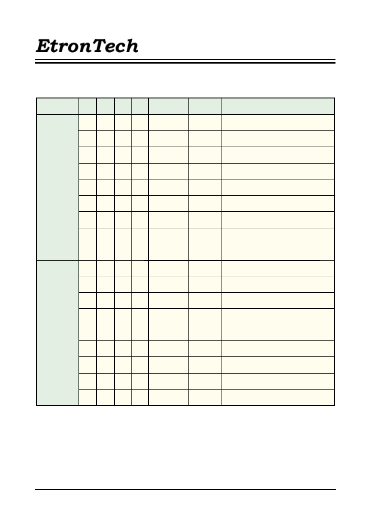
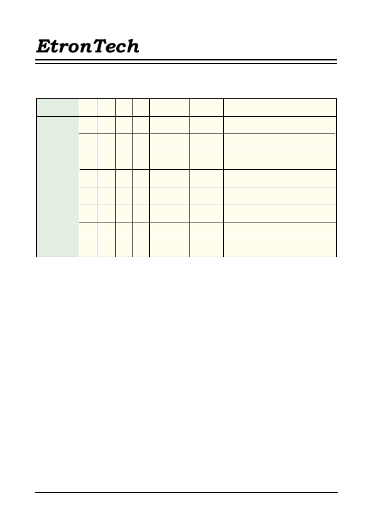
FUNCTION TRUTH T ABLE
Current State /CS /RAS /CAS /WE Address Command Action
EM639165
IDLE
ROW
ACTIVE
HXXXX DESEL NOP
L H H H X NOP NOP
L H H L TBST ILLEGAL*2
L H L X BA, CA, A10
L L H H BA, RA ACT Bank Active, Latch RA
L L H L BA, A10
L L L H X REFA Auto-Refresh*5
LLLL
HXXXX DESEL NOP
L H H H X NOP NOP
L H H L TBST NOP
BA
Op-Code,
Mode-Add
BA
READ /
WRITE
PRE /
PREA
MRS Mode Register Set*5
ILLEGAL*2
NOP*4
L H L H BA, CA, A10
L H L L BA, CA, A10
L L H H BA, RA ACT Bank Active / ILLEGAL*2
L L H L BA, A10
L L L H X REFA ILLEGAL
LLLL
Op-Code,
Mode-Add
READ /
READA
WRITE /
WRITEA
PRE /
PREA
MRS ILLEGAL
Begin Read, Latch CA, Determine
Auto-Precharge
Begin Write, Latch CA, Determine
Auto-Precharge
Precharge / Precharge All
Preliminary Rev 1.0 Feb. 2001
6
Page 7
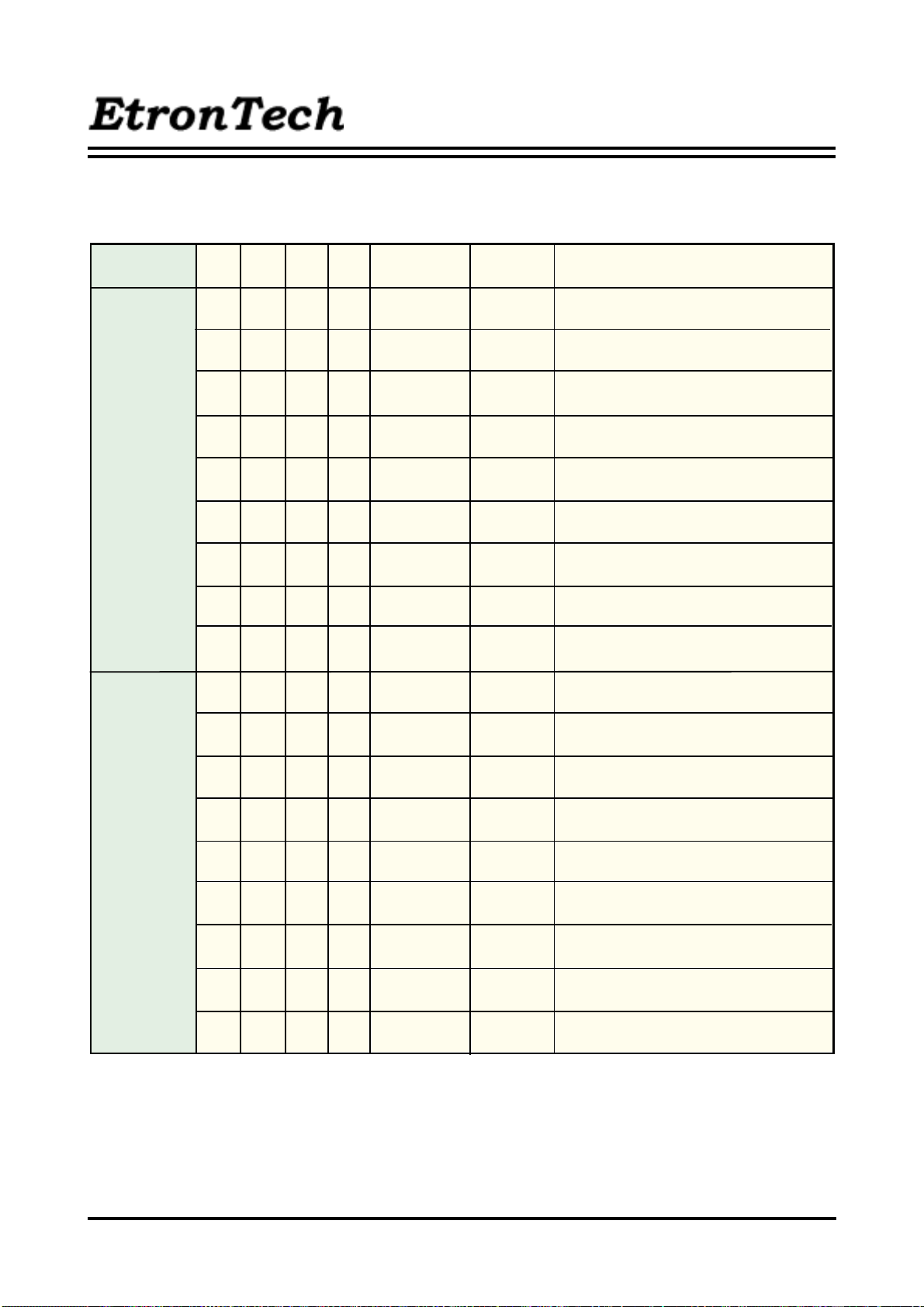
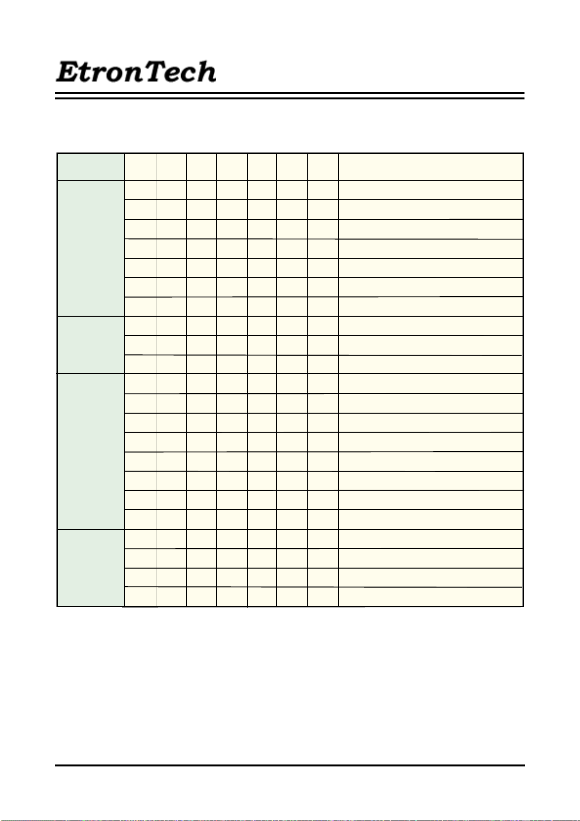
FUNCTION TRUTH T ABLE (continued)
EM639165
Current State /CS /RAS /CAS /WE Address
READ
WRITE
H X X X X DESEL
LHHHX NOP
L H H L TBST
L H L H BA, CA, A10
L H L L BA, CA, A10
L L H H BA, RA ACT
L L H L BA, A10
L L L H X REFA ILLEGAL
LLLL
H X X X X DESEL
L H H H X NO P NOP (Continue Burst to END)
BA
Op-Code,
Mode-Add
Command
READ
/READA
WRITE /
WRITEA
PRE /
PREA
MRS ILLEGAL
Action
NOP (Continue Burst to END)
NOP (Continue Burst to END)
Terminate Burst
Terminate Burst, Latch CA,Begin
Read, Determine Auto-Precharge*3
Terminate Burst, Latch CA,Begin
Write, Determine Auto-Precharge*3
Bank Active / ILLEGAL*2
Terminate Burst, Precharge
NOP (Continue Burst to END)
L H H L TBST
L H L H BA, CA, A10
L H L L BA, CA, A10
L L H H BA, RA ACT Bank Active / ILLEGAL*2
L L H L BA, A10
L L L H X REFA ILLEGAL
L L L L MRS ILLEGAL
BA
READ /
READA
WRITE /
WRITEA
PRE /
PREA
Op-Code,
Mode-Add
Terminate Burst, Latch CA,Begin
Terminate Burst, Latch CA,Begin
Read, Determine Auto-Precharge*3
Terminate Burst, Latch CA,Begin
Write, Determine Auto-Precharge*3
Terminate Burst, Precharge
Preliminary Rev 1.0 Feb. 2001
7
Page 8
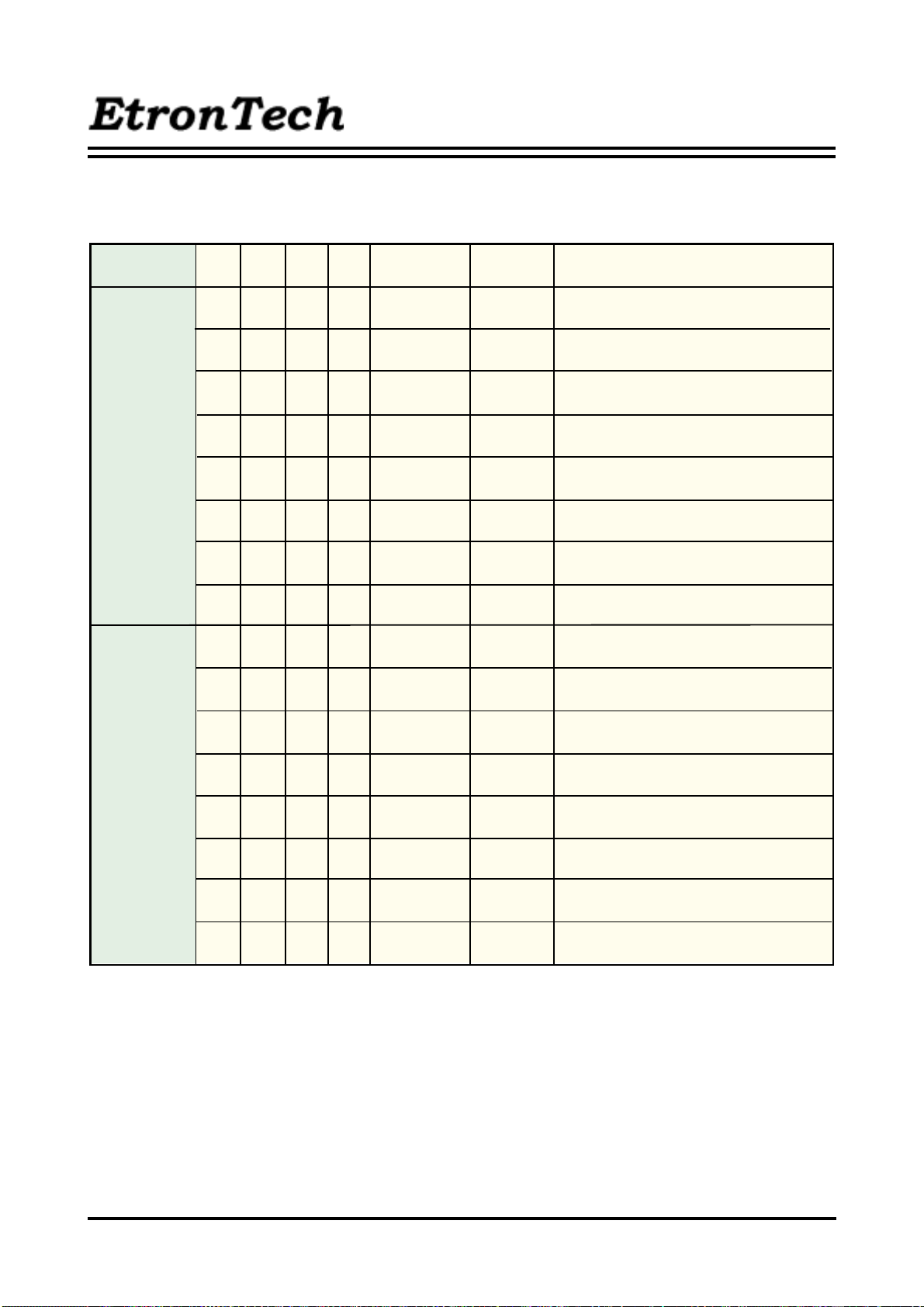
FUNCTION TRUTH T ABLE (continued)
Current State /CS /R AS /C AS /WE Address Command Action
EM639165
READ with
AUTO
PRECHARGE
WRITE with
AUTO
PRECHARGE
H X X X X DESEL
LHHHX NOP
L H H L TBST ILLEGAL
L H L H BA, CA, A10
L H L L BA, CA, A10
L L H H BA, RA ACT
L L H L BA, A10
L L L H X REFA ILLEGAL
LLLL
H X X X X DESEL
L H H H X NOP NOP (Continue Burst to END)
BA
Op-Code,
Mode-Add
READ /
READA
WRITE /
WRITE A
PRE /
PREA
MRS ILLEGAL
NOP (Continue Burst to END)
NOP (Continue Burst to END)
ILLEGAL
ILLEGAL
Bank Active / ILLEGAL*2
ILLEGAL*2
NOP (Continue Burst to END)
L H H L TBST ILLEGAL
L H L H BA, CA, A10
L H L L BA, CA, A10
L L H H BA, RA ACT
L L H L BA, A10
L L L H X REFA ILLEGAL
LLLL
BA
Op-Code,
Mode-Add
READ /
READA
WRITE /
WRITEA
PRE /
PREA
MRS
ILLEGAL
ILLEGAL
Bank Active / ILLEGAL*2
ILLEGAL*2
ILLEGAL
Preliminary Rev 1.0 Feb. 2001
8
Page 9
FUNCTION TRUTH T ABLE (continued)
Current State /CS /RAS /C AS /WE Address Command Action
EM639165
PRE -
CHARGING
ROW
ACTIVATING
H X X X X DESEL NOP (Idle after tRP)
L H H H X NOP NOP (Idle after tRP)
L H H L TBST ILLEGAL*2
L H L X BA, CA, A10
L L H H BA, RA ACT ILLEGAL*2
L L H L BA, A10
L L L H X REFA ILLEGAL
LLLL
H X X X X DESEL NOP (Row Active after tRCD)
L H H H X NOP NOP (Row Active after tRCD)
L H H L TBST ILLEGAL*2
BA
Op-Code,
Mode-Add
BA
READ /
WRITE
PRE /
PREA
MRS ILLEGAL
ILLEGAL*2
NOP*4 (Idle after tRP)
L H L X BA, CA, A10
L L H H BA, RA ACT
L L H L BA, A10
L L L H X REFA ILLEGAL
LLLL
Op-Code,
Mode-Add
READ /
WRITE
PRE /
PREA
MRS ILLEGAL
ILLEGAL*2
ILLEGAL*2
ILLEGAL*2
Preliminary Rev 1.0 Feb. 2001
9
Page 10
FUNCTION TRUTH T ABLE (continued)
Current State /CS /RAS /C AS /WE Address Command Action
EM639165
WRITE
RECOVERING
REFRESHING
HXXX
LHHH
LHHL
LHLX
LLHH
LLHL
L L L H X REFA ILLEGAL
LLLL
H X X X X DESEL NOP (Idle after tRC)
L H H H X NOP NOP (Idle after tRC)
L H H L TBST ILLEGAL
X
X NOP NOP
BA
BA, CA, A10
BA, RA ACT
BA, A10
Op-Code,
Mode-Add
BA
DESEL
TBST
READ /
WRITE
PRE /
PREA
MRS
NOP
ILLEGAL*2
ILLEGAL*2
ILLEGAL*2
ILLEGAL*2
ILLEGAL
L H L X BA, CA, A10
L L H H BA, RA ACT ILLEGAL
L L H L BA, A10
L L L H X REFA ILLEGAL
LLLL
Op-Code,
Mode-Add
READ /
WRITE
PRE /
PREA
MRS ILLEGAL
ILLEGAL
ILLEGAL
Preliminary Rev 1.0 Feb. 2001
10
Page 11
FUNCTION TRUTH T ABLE (continued)
Current State /CS /RAS /CAS /WE Address Command Action
EM639165
MODE
REGISTER
SETTING
H X X X X DESEL NOP (Idle after tRSC)
L H H H X NOP NOP (Idle after tRSC)
L H H L TBST ILLEGAL
L H L X BA, CA, A10
L L H H BA, RA ACT ILLEGAL
L L H L BA, A10
L L L H X REFA ILLEGAL
LLLL
BA
Op-Code,
Mode-Add
READ /
WRITE
PRE /
PREA
MRS ILLEGAL
ILLEGAL
ILLEGAL
Preliminary Rev 1.0 Feb. 2001
11
Page 12
FUNCTION TRUTH T ABLE for CKE
EM639165
Current State
SELF-
REFRESH*1
POWER
DOWN
ALL BANKS
IDLE*2
CKE
CKE
n-1
H X X X X X X INVALID
L H H X X X X Exit Self-Refresh (Idle after tRC)
LHLHHHX
L H L H H L X ILLEGAL
L H L H L X X ILLEGAL
L H L L X X X ILLEGAL
L L X X X X X NOP (Maintain Self-Refresh)
HXXXXXX
L H X X X X X Exit Power Down to Idle
L L X X X X X NOP (Maintain Power Down)
H H X X X X X Refer to Function Truth Table
H L L L L H X Enter Self-Refresh
H L H X X X X Enter Power Down
H L L H H H X Enter Power Down
/CS /RAS /CAS /WE Add Action
n
Exit Self-Refresh (Idle after tRC)
INVALID
H L L H H L X ILLEGAL
H L L H L X X ILLEGAL
H L L L X X X ILLEGAL
L X X X X X X Refer to Current State =Power Down
ANY STATE
other than
listed above
ABBREVIATIONS:
H=High Level, L=Low Level, X=Don't Care
NOTES:
1. CKE Low to High transition will re-enable CLK and other inputs asynchronously. A minimum
setup time must be satisfied before any command other than EXIT.
2. Power-Down and Self-Refresh can be entered only from the All Banks Idle State.
3. Must be legal command.
H H X X X X X Refer to Function Truth Table
H L X X X X X Begin CLK Susspend at Next Cycle*3
LHXXXXX
L L X X X X X Maintain CLK Suspend
Exit CLK Susspend at Next Cycle*3
Preliminary Rev 1.0 Feb. 2001
12
Page 13
EM639165
POWER ON SEQUENCE
Before starting normal operation, the following power on
sequence is necessary to prevent a SDRAM from damaged
or malfunctioning.
1. Apply power and start clock. Attempt to maintain CKE
high, DQM high and NOP condition at the inputs.
2. Maintain stable power, stable clock, and NOP input conditions for a minimum of 200µs.
3. Issue precharge commands for all banks. (PRE or PREA)
4. After all banks become idle state (after tRP), issue 8 or
more auto-refresh commands.
5. Issue a mode register set command to initialize the mode
register.
After these sequence, the SDRAM is idle state and ready
for normal operation.
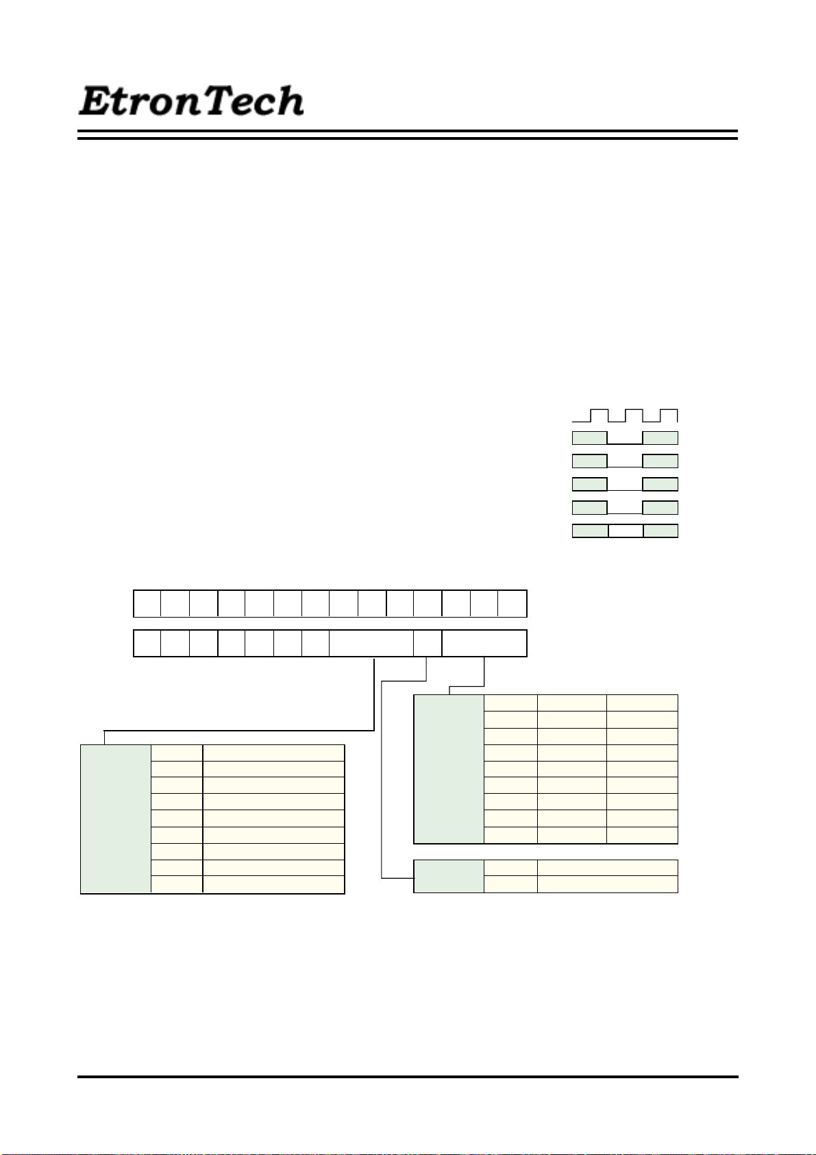
MODE REGISTER
Burst Length, Burst Type and /CAS Latency can be programmed by setting the mode register (MRS). The mode
register stores these data until the next MRS command,
which may be issued when all banks are in idle state. After
tRSC from a MRS command, the SDRAM is ready for new
command.
CLK
/CS
/RAS
/CAS
/WE
BA0,1 A11-A0
V
LATENCY
MODE
A11 A1 0 A9 A8 A7 A6 A5 A4 A3 A2 A1 A0BA1BA0
0 0 0 0 0 LTMODE BT BL00
CL
0 0 0
0 0 1
0 1 0
0 1 1
1 0 0
1 0 1
1 1 0
1 1 1
/CAS LATENCY
R: Reserved for Future Use
FP: Full Page
BL
0 0 0
0 0 1
R
R
2
3
R
R
R
R
BURST
LENGTH
BURST
TYPE
0 1 0
0 1 1
1 0 0
1 0 1
1 1 0
1 1 1
0
1
BT= 0 BT= 1
1
2
4
8
R
R
R
FP
SEQUENTIAL
INTERLEAVED
1
2
4
8
R
R
R
R
Preliminary Rev 1.0 Feb. 2001
13
Page 14
CLK
EM639165
Command
Address
DQ
Initial Address
A2 A1 A0
00 0
00 1
01 0
01 1
10 0
CL= 3
BL= 4
BL
8
Read
Y
Q0 Q1 Q2 Q3
/CAS Latency Burst Length Burst Length
Burst Type
Column Addressing
Sequential Interleaved
0123456701234567
1234567010325476
2345670123016745
3456701232107654
4567012345670123
Write
Y
D0 D1 D2 D3
10 1
11 0
11 1
-00
-01
-10
-11
--0
--1
5670123454761032
6701234567452301
7012
0123
1230
4
2301
30
01
2
10
3456 3210
12
7654
0123
1032
2301
32
01
10
10
Preliminary Rev 1.0 Feb. 2001
14
Page 15
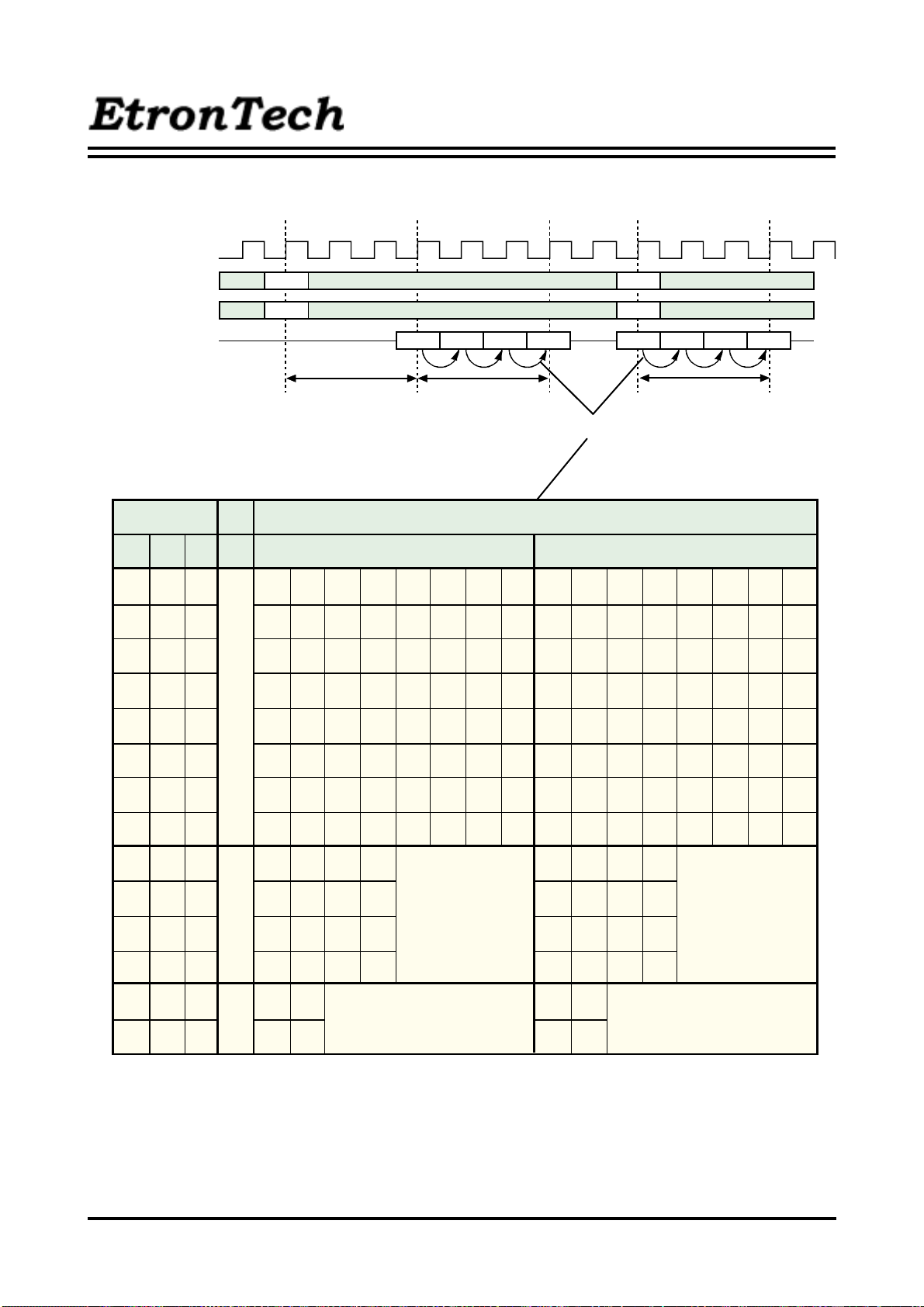
OPERATIONAL DESCRIPTION
BANK ACTIVATE
The SDRAM has four independent banks. Each bank is activated by
the ACT command with the bank addresses (BA0,1). A row is indicated by the row addresses A0-11. The minimum activation interval
between one bank and the other bank is tRRD. Maximum 2 ACT
commands are allowed within tRC , although the number of banks
which are active concurrently is not limited.
PRECHARGE
The PRE command deactivates the bank indicated by BA0,1. When
multiple banks are active, the precharge all command (PREA, PRE
+ A10=H) is available to deactivate them at the same time.
After tRP from the precharge, an ACT command to the same bank
can be issued.
READ
After tRCD from the bank activation, a READ command can be
issued. 1st output data is available after the /CAS Latency from the
READ, followed by (BL -1) consecutive data when the Burst Length
is BL. The start address is specified by A0-A9,A11(x4), A0-9(X8),
A0-8(X16) , and the address sequence of burst data is defined by
the Burst Type. A READ command may be applied to any active
bank, so the row precharge time (tRP) can be hidden behind
continuous output data by interleaving the multiple banks. When
A10 is high at a READ command, the auto-precharge (READA) is
performed. Any command (READ, WRITE, PRE, TBST, ACT) to
the same bank is inhibited till the internal precharge is complete.
The internal precharge starts at BL after READA. (Need to keep
tRAS min.) The next ACT command can be issued after (BL +
tRP) from the previous READA.
Bank Activation and Precharge All (BL=4, CL=3)
EM639165
CLK
Command
A0-9
A10
A11
BA0,1
DQ
2 ACT command / tRCmin
ACT
tRRD
Xa
tRCD
Xa
Xa Xb Xb
00
ACT
Xb
Xb
01
READ
Y
0
00
tRCmin
tRAS
PRE
tRP
1
Qa0 Qa1 Qa2 Qa3
Precharge all
ACT
Xb
Xb
01
Preliminary Rev 1.0 Feb. 2001
15
Page 16

Multi Bank Interleaving READ (BL=4, CL=3)
CLK
EM639165
Command
A0-9
A10
A11
BA0,1
ACT
tRCD
Xa
Xa
Xa Xb
00
READ
Y
0
00
ACT
Xb
Xb
10
DQ
/CAS latency
READ with Auto-Precharge (BL=4, CL=3)
CLK
Command
A0-9
A10
ACT
Xa
Xa
READ
tRCD
Y
1
READ
Qa0 Qa1 Qa2 Qa3 Qb0 Qb1 Qb2
Burst Length
BL + tRP
BL
10
PRE
Y
0
0
00
ACT
tRP
Xa
Xa
A11
BA0,1
Xa Xa
00
00
DQ
READ Auto-Precharge Timing (BL=4)
CLK
Command
CL=3
CL=2
DQ
DQ
ACT READ
00
Qa0 Qa1 Qa2 Qa3
Internal precharge start
BL
Qa1 Qa2 Qa3Qa0
Qa1 Qa2 Qa3Qa0
Internal Precharge Start Timing
Preliminary Rev 1.0 Feb. 2001
16
Page 17

WRITE
After tRCD from the bank activation, a WRITE command
can be issued. 1st input data is set at the same cycle as the
WRITE. Following (BL -1) data are written into the RAM,
when the Burst Length is BL. The start address is specified
by A0-A9,A11(x4), A0-9(X8), A0-8(X16) and the address
sequence of burst data is defined by the Burst Type. A
WRITE command may be applied to any active bank, so
the row precharge time (tRP) can be hidden behind continuous input data by interleaving the multiple banks. From
WRITE with Auto-Precharge (BL=4)
CLK
EM639165
the last input data to the PRE command, the write recovery
time (tWR) is required. When A10 is high at a WRITE
command, the autoprecharge (WRITEA) is performed. Any
command (READ, WRITE, PRE, TBST, ACT) to the same
bank is inhibited till the internal precharge is complete. The
internal precharge begins at tWR after the last input data
cycle. (Need to keep tRAS min.) The next ACT command
can be issued after tRP from the internal precharge timing.
Command
A0-9
A10
A11
BA0,1
DQ
CLK
Command
A0-9
A10
ACT
Xa
Xa
Xa
Xa
00
ACT
Xa
Xa
10
PRE
Y
0
0
00
Write
tRCD tRCD
ACT
Y
Xb
00
Xb
Xb 0Xa
00
10
Da1 Da2 Da3 Db0 Db1 Db2 Db3
Da0
Write
Multi Bank Interleaving WRITE (BL=4)
Write
tRCD
Y
1
PRE
0
10
ACT
tRP
Xa
Xa
A11
BA0,1
DQ
Preliminary Rev 1.0 Feb. 2001
Xa Xa
00
00
tWR
Da0 Da1 Da2 Da3
Internal precharge starts
17
00
Page 18

EM639165
BURST INTERRUPTION [ Read Interrupted by Read ]
Burst read operation can be interrupted by new read of any bank. Random column access is allowed READ to READ interval
is minimum 1 CLK..
Read Interrupted by Read (BL=4, CL=3)
CLK
READ
Command
A0-9
READ
Yi
Yj Yk Yl
READ
READ
A10
A11
BA0,1
DQ
0000
00 1000 01
Qai0 Qaj1 Qbk0 Qbk1Qaj0 Qbk2 Qal0 Qal1 Qal2 Qal3
[ Read Interrupted by Write ]
Burst read operation can be interrupted by write of any bank. Random column access is allowed. In this case, the DQ
should be controlled adequately by using the DQM to prevent the bus contention. The output is disabled automatically 1
cycle after WRITE assertion.
Read Interrupted by Write (BL=4, CL=3)
CLK
Command
A0-9
A10
READ
Yi
0
Write
Yj
0
A11
BA0,1
DQM
Q
D
00
Qai0
DQM control Write control
Preliminary Rev 1.0 Feb. 2001
00
Daj0 Daj1 Daj2 Daj3
18
Page 19

[ Read Interrupted by Precharge ]
Burst read operation can be interrupted by precharge of the
same bank . READ to PRE interval is minimum 1 CLK. A PRE
command to output disable latency is equivalent to the /CAS
Read Interrupted by Precharge (BL=4)
CLK
EM639165
Latency. As a result, READ to PRE interval determines valid
data length to be output. The figure below shows examples of
BL=4.
CL=3
CL=2
Command
DQ
Command
DQ
Command
DQ
Command
DQ
Command
DQ
Command
READ
READ
READ
READ
READ PRE
READ PRE
PRE
PRE
Q0 Q1 Q2
Q0
PRE
Q0 Q1 Q2
Q0
Q1
Q0
PRE
Q1
DQ
Preliminary Rev 1.0 Feb. 2001
Q0
19
Page 20

EM639165
[Read Interrupted by Burst Terminate]
Similarly to the precharge, a burst terminate command can interrupt the burst read operation and disable the data output. The
terminated bank remains active.
Read Interrupted by Terminate (BL=4)
CLK
CL=3
Command
DQ
Command
DQ
READ
READ
TBST
READ to TBST interval is minimum 1 CLK. A TBST command to
output disable latency is equivalent to the /CAS Latency.
TBST
Q0 Q1 Q2
Q0
Q1
CL=2
Command
DQ
Command
DQ
Command
DQ
Command
DQ
READ
READ
READ
READ
TBST
TBST
Q0
TBST
Q0 Q1 Q2
TBST
Q0
Q1
Q0
Preliminary Rev 1.0 Feb. 2001
20
Page 21

EM639165
[ Write Interrupted by Write ]
Burst write operation can be interrupted by new write of any bank. Random column access is allowed. WRITE to WRITE
interval is minimum 1 CLK.
Write Interrupted by Write (CL=3,BL=4)
CLK
Command
A0-9
A10
Write
Yi
0
Write
Yj
0
Write
Yk
0
Write
Yl
0
A11
BA0,1
DQ
00
00
Dai0 Daj0 Daj1 Dbk0
10
Dbk1 Dbk2
00
Dal0 Dal1 Dal2 Dal3
[ Write Interrupted by Read ]
Burst write operation can be interrupted by read of the same or the other bank. Random column access is allowed. WRITE
to READ interval is minimum 1 CLK. The input data on DQ at the interrupting READ cycle is "don't care".
Write Interrupted by Read (CL=3,BL=4)
CLK
Command
A0-9
A10
Write
Yi
0
READ
Yj
0
Write
Yk
0
READ
Yl
0
A11
BA0,1
00
00
10
00
DQM
Qaj0
DQ
Preliminary Rev 1.0 Feb. 2001
Qaj1Dai0 Dbk0 Dbk1
21
Qal0
Page 22

EM639165
[ Write Interrupted by Precharge ]
Burst write operation can be interrupted by precharge of the same bank.Write recovery time(tWR) is required from the last data
to PRE command. During write recovery, data inputs must be masked by DQM.
Write Interrupted by Precharge (BL=4)
CLK
Command
A0-9,11
A10
BA0-1
DQM
DQ
ACT
Xa
0
00
Write
Ya
0
00
Da0 Da 1
tWR
PRE
0
00
ACT
tRP
Xa
0
00
[Write Interrupted by Burst Terminate]
Burst terminate command can terminate burst write operation.In this case, the write recovery time is not required and the
bank remains active. WRITE to TBST interval is minimum 1 CLK.
Write Interrupted by Terminate (BL=4)
CLK
Command
A0-9,11
A10
BA0-1
DQ
ACT
Xa
0
00
Preliminary Rev 1.0 Feb. 2001
Write
Ya
0
00
Da0 Da 1
TBST Write
Yb
0
00
Db0 Db1 Db2 Db3
22
Page 23

EM639165
[Write with Auto-Precharge Interrupted by Write or Read to another Bank]
Burst write with auto-precharge can be interrupted by write or read to another bank. Next ACT command can be issued after
tRP. Auto-precharge interruption by a command to the same bank is inhibited.
Write Interrupted by WRITE to another bank (BL=4)
CLK
Command
A0-9,11
A10
BA0-1
DQ
CLK
Command
Write
Ya
1
00
Da0 Da1
Write
BL
Yb
tWR
0
10
Db0 Db 1 Db2 Db3
interruptedauto-precharge activate
ACT
tRP
Xa
Xa
00
Write Interrupted by READ to another bank (CL=2,BL=4)
Write
Read
BL
ACT
tRP
A0-9,11
A10
BA0-1
DQ
Preliminary Rev 1.0 Feb. 2001
Ya
1
00
Da0 Da1
Yb
tWR
0
10
Qb0 Qb1 Qb2 Qb3
interruptedauto-precharge activate
23
Xa
Xa
00
Page 24

EM639165
[Read with Auto-Precharge Interrupted by Read to another Bank]
Burst write with auto-precharge can be interrupted by write or read to another bank. Next ACT command can be issued after
tRP. Auto-precharge interruption by a command to the same bank is inhibited.
Read Interrupted by Read to another bank (CL=2,BL=4)
CLK
Command
A0-9,11
A10
BA0-1
DQ
Read
Ya
1
00
Read
BL tRP
Yb
0
10
Qa0 Qa1
interruptedauto-precharge activate
Qb0 Qb1 Qb2 Qb3
ACT
Xa
Xa
00
[Full Page Burst]
Full page burst length is available for only the sequential burst type. Full page burst read or write is repeated untill a Precharge
or a Burst Terminate command is issued. In case of the full page burst, a read or write with auto-precharge command is illegal.
[Single Write]
When single write mode is set, burst length for write is always one, independently of Burst Length defined by (A2-0).
Preliminary Rev 1.0 Feb. 2001
24
Page 25

AUTO REFRESH
Single cycle of auto-refresh is initiated with a REFA (/CS= /RAS= /
CAS= L, /WE= /CKE= H) command. The refresh address is generated internally. 4096 REFA cycles within 64ms refresh
128M bit memory cells. The auto-refresh is performed on 4
banks concurrently. Before performing an auto-refresh, all
Auto-Refresh
CLK
EM639165
banks must be in the idle state. Auto-refresh to auto-refresh
interval is minimum tRC. Any command must not be supplied to the device before tRC from the REFA command.
/CS
/RAS
/CAS
/WE
CKE
A0-11
BA0,1
Auto Refresh on All Banks
NOP or DESELECT
minimum tRFC
Auto Refresh on All Banks
Preliminary Rev 1.0 Feb. 2001
25
Page 26

SELF REFRESH
Self-refresh mode is entered by issuing a REFS command
(/CS= /RAS= /CAS= L, /WE= H, CKE= L). Once the selfrefresh is initiated, it is maintained as long as CKE is kept
low. During the self-refresh mode, CKE is asynchronous and
the only enabled input ,all other inputs including CLK are
disabled and ignored, so that power consumption due to
Self-Refresh
CLK
/CS
/RAS
/CAS
EM639165
synchronous inputs is saved. To exit the self-refresh, supplying
stable CLK inputs, asserting DESEL or NOP command and then
asserting CKE=H. After tRC from the 1st CLK egde following
CKE=H, all banks are in the idle state and a new command can be
issued, but DESEL or NOP commands must be asserted till then.
Stable CLK
NOP
/WE
CKE
A0-11
BA0,1
Self Refresh Entry
Self Refresh Exit
new command
X
00
minimum tRFC
for recovery
Preliminary Rev 1.0 Feb. 2001
26
Page 27

CLK SUSPEND
CKE controls the internal CLK at the following cycle. Figure
below shows how CKE works. By negating CKE, the next
internal CLK is suspended. The purpose of CLK suspend is
power down, output suspend or input suspend. CKE is a
ext.CLK
tIH tIS tIH tIS
CKE
int.CLK
EM639165
synchronous input except during the self-refresh mode. CLK
suspend can be performed either when the banks are active
or idle. A command at the suspended cycle is ignored.
CLK
CKE
Command
CKE
Command
CLK
CKE
Power Down by CKE
PRE NOP NOP NOP
NOP NOP NOPACT
DQ Suspend by CKE (CL=2)
Standby Power Down
Active Power Down
Command
DQ
Preliminary Rev 1.0 Feb. 2001
Write Read
D0 D1 D2 D3
27
Q0 Q1 Q2 Q3
Page 28

DQM CONTROL
DQM is a dual function signal defined as the data mask for
writes and the output disable for reads. During writes, DQM(U,L)
masks input data word by word. DQM(U,L) to write mask latency
DQM Function(CL=3)
CLK
EM639165
is 0. During reads, DQM(U,L) forces output to Hi-Z word by word.
DQM(U,L) to output Hi-Z latency is 2.
Command
DQM
DQ
Write
D0 D2 D3
masked by DQM(U,L)=H
READ
Q0 Q1 Q3
disabled by DQM(U,L)=H
Preliminary Rev 1.0 Feb. 2001
28
Page 29

ABSOLUTE MAXIMUM RATINGS
EM639165
Symbol Parameter
VDD
VDDQ
VI
VO
IO
Pd
Topr
Tstg
Supply Voltage
Supply Voltage for Output
Input Voltage
Output Voltage -0.5 - 4.6
Output Current
Power Dissipation
Operating Temperature
Storage Temperature
Condition Rating Unit
with respect to VSS
with respect to VSSQ
with respect to VSS
with respect to VSSQ
Ta = 25˚C
RECOMMENDED OPERATING CONDITIONS
(Ta=0 - 70
˚C ,unless otherwise noted)
Symbol
VDD
VSS 0
VDDQ Supply Voltage for output 3.0
VSSQ
VIH*1
VIL*2
Supply Voltage
Supply Voltage
Supply Voltage for output
High-Level Input Voltage all inputs
Low-level Input Voltage all inputs
Parameter
Min.
3.0
0
2.0
-0.3
-0.5 - 4.6
-0.5 - 4.6
-0.5 - 4.6
50
1000
0 - 70
-65 - 150
Typ. Max.
3.3
0
3.3
0
3.6 V
3.6 V
0
VDDQ +0.3
0.8 V
V
V
V
V
mA
mW
˚C
˚C
Unit
V
V
V
NOTES:
1. VIH(max)=5.5V for pulse width less than 10ns.
2. VIL(min)=-1.0V for pulse width less than 10ns.
CAPACITANCE
(Ta=0 -70˚C,VDD=VDDQ=3.3±0.3V,VSS=VSSQ=0V,unless otherwise noted)
Symbol
CI(A)
CI(C)
CI(K)
CI/O Input Capacitance, I/O pin
Parameter
Input Capacitance, address pin
Input Capacitance, contorl pin
Input Capacitance, CLK pin
Preliminary Rev 1.0 Feb. 2001
Test Condition
@ 1MHz
1.4V bias
200mV swing
Vcc=3.3V
29
Min.
2.5
2.5
2.5
4.0
Max.
5.0
5.0
4.0
6.5
Unit
pF
pF
pF
pF
Page 30

AVERAGE SUPPLY CURRENT from Vdd
(Ta=0 - 70˚C, VDD=VDDQ=3.3±0.3V,VSS=VSSQ=0V, unless otherwise noted)
EM639165
ITEM
Operating current
Precharge Standby
current in Non-Power
down mode
Precharge Standby
current in Power down
mode
Active Standby current
Burst current
Auto-refresh current
Self-refresh current
Symbol
Icc1
Icc2N
Icc2NS
Icc2P
Icc2PS
Icc3N
Icc3NS
Icc4
Icc5
Icc6
Test Condition
tRC=min, tCLK=min
BL=1,IOL=0mA
CKE=VILmax
tCLK=15ns
CKE=VIHmin
CLK=VILmax(fixed)
CKE=VIHmin
tCLK=15ns(Note)
CKE=VIHmin
tCLK=VILmax(fixed)
CKE=/CS=VIHmin
tCLK=15ns(Note)
CKE=VIHmin
tCLK=VILmax(fixed)
All Bank Active
tCLK = min
BL=4, CL=3, IOL=0mA
tRC=min, tCLK=min
CKE < 0.2V
Standard
Low-Power
Max.
-75
100
110
130
20
15
2
1
30
20
160 130
160 160
22
800 800
-8
95
100
120
20
15
2
1
30
20
Unit
mA
mA
mA
mA
mA
mA
mA
mA
mA
mA
mA
µA
NOTE:
1. Icc(max) is specified at the output open condition.
2. Input signals are changed one time during 30ns.
AC OPERATING CONDITIONS AND CHARACTERISTICS
(Ta=0 - 70˚C, VDD=VSSQ=3.3±0.3V,VSS=VSSQ=0V, unless otherwise noted)
Symbol
VOH (DC)
VOL (DC)
IOZ
I
I
High-Level Output Voltage (DC)
Low-level Output Voltage (DC)
Off-state Output Current
Input Current
Parameter Test Conditions
IOH=-2mA
IOL= 2mA
Q floating VO= 0 -- VDDQ
VIH = 0 -- VDDQ +0.3V
Min.
2.4
-10
-10 10
Max.
0.4
10
Unit
V
V
µA
µA
Preliminary Rev 1.0 Feb. 2001
30
Page 31

AC TIMING REQUIREMENTS
(Ta=0 - 70˚C, VDD=VDDQ=3.3±0.3V,VSS=VSSQ=0V, unless otherwise noted)
Input Pulse Levels:0.8V-2.0V
Input Timing Measurement Level:1.4V
EM639165
Symbol
tCLK
CLK cycle time
Parameter
tCH CLK High pulse width
tCL CLK Low pulse width
tT
tIS
tIH Input Hold time
Transition time of CLK
Input Setup time
(all inputs)
(all inputs) n
tRC Row Cycle time
tRFC Refresh Cycle Time
tRCD Row to Column Delay
tRAS Row Active time
tRP Row Precharge time
tWR Write Recovery time
tRRD
tRSC
Act to Act Delay time
Mode Register Set Cycle time
CL=2
CL=3
Min.
10
7.5
2.5
2.5
1
1.8
1
67.5
75
20
45
20
15
15
15
-75
Max.
10
100K
Min.
10
8
3
3
1
2
1
70
80
20
48
20
20
20
20
-8
Max.
10
100K
Unit
ns
ns
n
s
s
n
ns
ns
s
ns
ns
ns
ns
ns
ns
ns
ns
tREF Refresh Interval time
CLK
DQ
1.4V
1.4V
64
Any AC timing is referenced
64
ms
to the input signal passing
through 1.4V.
Preliminary Rev 1.0 Feb. 2001
31
Page 32

V
SWITCHING CHARACTERISTICS
(Ta=0 - 70˚C, VDD=VDDQ=3.3±0.3V,VSS=VSSQ=0V, unless otherwise noted)
EM639165
Min.
3
3
0
3
-75
Max.
6
5.4
5.4
Min.
3
3
0
3
Symb ol Parameter
tAC
Access time from CLK
Output Hold time
tOH
from CLK
tOLZ
tOHZ
NOTE:
1. If clock rising time is longer than 1ns,(tr/2-0.5ns) should be added to the parameter.
Delay time , output lowimpedance from CLK
Delay time , output highimpedance from CLK
CL=2
CL=3
CL=2
CL=3
Output Load Condition
-8
Max.
6
6
6
Unit
ns
ns
ns
ns
ns
ns
Note
*1
OUT
50pF
CLK
DQ
tOLZ
tAC
tOH
CLK
DQ
Output Timing Measurement
Reference Point
tOHZ
1.4V
1.4V
1.4V
1.4V
Preliminary Rev 1.0 Feb. 2001
32
Page 33

Burst Write (single bank) @BL=4
/
/
/
/
0 1 2 3 4 5 6 7 8 9 10 11 12 13 14 15 16
CLK
CS
EM639165
tRC
tRAS
tRP
RAS
tRCD
tRCD
CAS
tWR
tWR
WE
CKE
DQM
A0-8
X
Y
X Y
A10
X
X
A9,11
BA 0,1
DQ
Preliminary Rev 1.0 Feb. 2001
X
0
ACT#0 PRE#0 ACT#0 WRITE#0 PRE#0
0
D0 D0 D0 D0
WRITE#0
0
33
X
0 0
0
D0 D0 D0 D0
Page 34

Burst Write (multi bank) @BL=4
/
/
/
/
0 1 2 3 4 5 6 7 8 9 10 11 12 13 14 15 16
CLK
CS
tRAS
tRRD
RAS
EM639165
tRC
tRC
tRP
tRCD
tRCD
tRCD
CAS
tWR
tWR
WE
CKE
DQM
A0-8
X
Y
X
Y
X Y
X
A10
A9,11
BA0,1
X
X
0
X
X
0
1
0
1
X
X
0 0
X
X
1
0
DQ
ACT#0 WRITE#0 PRE#0 ACT#0 WRITE#0 PRE#0
D0 D0 D0 D0
ACT#1
Preliminary Rev 1.0 Feb. 2001
D1 D1 D1 D1
WRITEA#1
(Auto-Precharge)
34
D0 D0 D0 D0
ACT#1
Page 35

Burst Read (single bank) @BL=4 CL=2
/
/
/
/
0 1 2 3 4 5 6 7 8 9 10 11 12 13 14 15 16
CLK
tRC
CS
EM639165
tRAS tRP
tRAS
RAS
tRCD
tRCD
CAS
WE
CKE
DQM
A0-8
X
Y
X Y
A10
X
X
A9,11
BA 0,1
DQ
Preliminary Rev 1.0 Feb. 2001
X
0
ACT#0 READ#0 PRE#0 ACT#0 READ#0 PRE#0
0
Q0 Q0 Q0 Q0
0
35
X
0 0
0
Q0 Q0 Q0 Q0
Page 36

Burst Read (multiple bank) @BL=4 CL=2
/
/
/
/
0 1 2 3 4 5 6 7 8 9 10 11 12 13 14 15 16
CLK
tRC
CS
EM639165
tRC
tRRD
tRAS
RAS
tRCD tRCD
tRCD
CAS
WE
CKE
DQM
A0-8
X
Y
X
Y
X Y
X
A10
X
X
X
X
A9,11
BA 0,1
DQ
X
0
ACT#0 READA#0
0
X
1
ACT#1
1
Q0 Q0 Q0 Q0
READA#1
Preliminary Rev 1.0 Feb. 2001
X
0 0
Q1 Q1 Q1 Q1
ACT#0 READ#0 PRE#0
X
1
Q0 Q0 Q0 Q0
ACT#1
0
36
Page 37

EM639165
/
/
/
/
Write Interrupted by Write @BL=4
0 1 2 3 4 5 6 7 8 9 10 11 12 13 14 15 16
CLK
CS
tRRD
RAS
tRCD
CAS
tWR
WE
CKE
DQM
A0-8
X
Y
X
Y
Y
Y
X
A10
A9,11
BA0,1
DQ
X
X
0
ACT#0 WRIT E#0 WRITE#0 PRE#0
X
X
0
1
D0 D0 D0 D0
ACT#1
0
WRITE#0 WRITEA#1
interrupt
same
bank
1
D0 D1 D1 D1
interrupt
other
bank
0
D0 D0 D0 D0
interrupt
other
bank
0
ACT#1
X
X
1
Preliminary Rev 1.0 Feb. 2001
37
Page 38

Read Interrupted by Read @BL=4,CL=2
/
/
/
/
0 1 2 3 4 5 6 7 8 9 10 11 12 13 14 15 16
CLK
CS
tRRD
RAS
EM639165
tRCD
tRCD
CAS
WE
CKE
DQM
A0-8
X
Y
X
Y
Y
Y
X
A10
A9,11
BA0,1
X
X
0
X
X
0
1
1
1
0
X
X
1
DQ
ACT#0 READ#0 READ# 0
ACT#1
Q0 Q0
READ#1 READA#1
interrupt
other
bank
Preliminary Rev 1.0 Feb. 2001
Q0 Q1 Q1 Q1
interrupt
same bank
38
Q1 Q1 Q0 Q0
interrupt
other
bank
Q0 Q0
ACT#1
Page 39

EM639165
/
/
/
/
Write Interrupted by Read, Read Interrupted by Write @BL=4,CL=2
0 1 2 3 4 5 6 7 8 9 10 11 12 13 14 15 16
CLK
CS
tRRD
RAS
tRCD
tRCD
CAS
tWR
WE
CKE
DQM
A0-8
A10
A9,11
BA0,1
DQ
X
X
X
0
ACT#0 WRITE#0 WRITE#1 PRE#1
X
X
X
1
Y
0
D0 D0
Y
1
READ#1
Q1 Q1
Y
1
D1 D1 D1 D1
1
ACT#1
Preliminary Rev 1.0 Feb. 2001
39
Page 40

Write/Read Terminated by Precharge @BL=4,CL=2
/
/
/
/
0 1 2 3 4 5 6 7 8 9 10 11 12 13 14 15 16
CLK
CS
EM639165
tRC
tRP
tRAS
tRP
RAS
tRCD
tRCD
CAS
tWR
WE
CKE
DQM
A0-8
A10
A9,11
X
X
X
Y
X
X
X
Y
X
X
X
BA 0,1
0
DQ
ACT#0 WRITE#0 READ# 0 PRE#0
Preliminary Rev 1.0 Feb. 2001
0
D0 D0
0
PRE#0
Terminate Terminate
0
ACT#0
0
0
Q0 Q0
40
0
ACT#0
Page 41

Write/Read Terminated by Burst Terminate @BL=4,CL=2
/
/
/
/
0 1 2 3 4 5 6 7 8 9 10 11 12 13 14 15 16
CLK
CS
RAS
tRCD
CAS
WE
EM639165
tWR
CKE
DQM
A0-8
X
Y
Y
Y
A10
A9,11
BA 0,1
DQ
X
X
0
0
D0 D0
0
Q0 Q0
0
D0 D0 D0 D0
0
ACT#0 WRITE#0 READ#0
TERM
Preliminary Rev 1.0 Feb. 2001
41
TERM
WRITE#0
PRE#0
Page 42

Single Write Burst Read @BL=4,CL=2
/
/
/
/
0 1 2 3 4 5 6 7 8 9 10 11 12 13 14 15 16
CLK
CS
RAS
tRCD
CAS
WE
EM639165
CKE
DQM
A0-8
X
Y
Y
A10
A9,11
BA 0,1
DQ
X
X
0
0
D0 Q0 Q0
0
Q0 Q0
ACT#0 WRITE#0 READ#0
Preliminary Rev 1.0 Feb. 2001
42
Page 43

Power-Up Sequesce and Intialize
/
/
/
/
CLK
200µs
CS
EM639165
tRP tRFC
tRFC tRSC
RAS
CAS
WE
CKE
DQM
A0-8
A10
A9,11
MA
0
0
X
X
X
BA0,1
0
0
DQ
NOP
Power On
Preliminary Rev 1.0 Feb. 2001
PRE ALL REFA ACT#0MRSREFA
Minimum 8 REFA cycles
43
REFA
Page 44

Auto Refresh
/
/
/
/
CLK
CS
RAS
CAS
WE
EM639165
0 1 2 3 4 5 6 7 8 9 10 11 12 13 14 15 16
tRFC
tRP
tRCD
CKE
DQM
A0-8
A10
A9,11
BA0,1
DQ
PRE ALL REFA
X
X
X
0
ACT#0
Y
0
D0 D0 D0 D0
WRITE#0
All banks must be idle before REFA is issued.
Preliminary Rev 1.0 Feb. 2001
44
Page 45

Self Refresh
/
/
/
/
CLK
CS
RAS
CAS
WE
EM639165
0 1 2 3 4 5 6 7 8 9 10 11 12 13 14 15 16
tRFC
tRP
CKE
DQM
A0-8,
A10
A9,11
BA0,1
X
X
X
0
DQ
PRE ALL Self Refresh Entry Self Refres h Exit
ACT#0
All banks must be idle before REFS is issued.
Preliminary Rev 1.0 Feb. 2001
45
Page 46

CLK Suspension @BL=4,CL=2
/
/
/
/
0 1 2 3 4 5 6 7 8 9 10 11 12 13 14 15 16
CLK
CS
RAS
tRCD
CAS
WE
EM639165
CKE
DQM
A0-8
A10
A9,11
BA0,1
DQ
X
X
X
0
ACT#0 WRITE#0 READ# 0
Y
0
D0 Q0 Q0
D0 D0 D0
internal
CLK
suspended
Y
0
Q0
internal
CLK
suspended
Q0
Preliminary Rev 1.0 Feb. 2001
46
Page 47

Power Down
/
/
/
/
CLK
CS
RAS
CAS
WE
EM639165
0 1 2 3 4 5 6 7 8 9 10 11 12 13 14 15 16
Standby Power Down Active Power Down
CKE
DQM
A0-8
X
A10
A9,11
BA 0,1
X
X
0
DQ
PRE ALL ACT#0
Preliminary Rev 1.0 Feb. 2001
47
Page 48

54 Pin TSOP II Package Outline Drawing Information
EM639165
54
1
D
S
B e
y
28
0.254
E
E
H
27
2
A
A
1
L
A
θ°
L
1
L
C
L
1
Symbol Dimension in inch Dimension in mm
Min Normal Max Min Normal Max
A --
A1
0.002 0.00395 0.0059 0.05 0.1 0.150
A2--
B
c
D
E
e
HE
L
L1
S
y
q
0.012 0.015 0.016 0.3 0.35 0.40
0.0047 0.0065 0.0083 0.120 1.165 0.210
0.872 0.8755 0.879 22.149 22.238 22.327
0.3960 0.400 0.4040 10.058 10.16 10.262
- 0.0315 - - 0.80 -
0.462 0.466 0.470 11.735 11.8365 11.938
0.016 0.020 0.0235 0.406 0.50 0.597
- 0.033 - - 0.84 -
- 0.035 - - 0.88 -
- - 0.004 - - 0.10
0°
-
0.047
0.0411
5° 0°
--
--
-
Notes:
1. Dimension D & E do not include interiead flash.
2. Dimension B does not include dambar protrusion/intrusion.
3. Dimension S includes end flash.
4. Controlling dimension: mm
1.194
1.044
5°
Preliminary Rev 1.0 Feb. 2001
48
 Loading...