

Datasheet EM565161BJ-70, EM565161BJ-55, EM565161BA-70E, EM565161BA-70, EM565161BA-55E Datasheet (ETRON)
...Page 1
Etr onT ech
EM565161
512K x 16 Low Power SRAM
Preliminary, Rev 0.9 01/2002
Features
Single Power Supply Voltage, 2.3 ~ 3.6 V
•
Power Down Features Using CE1#, CE2, LB# and
•
UB#
Low Power Dissipation
•
Data retention Supply Voltage: 1.0V to 3.6V
•
Direct TTL Compatibility for All Input and Output
•
Wide Operating Temperature Range: -40°C to 85°C
•
Standby current (maximum) @ VDD = 3.6 V
•
I
Part Number
EM565161BA/BJ-55
EM565161BA/BJ-70
EM565161BA/BJ-55E/70E
Typical Maximum
2 µA 35
2 µA 25
14 µA 80
DDS2
A
µ
A
µ
A
µ
Ordering Information
Part Number Speed I
EM565161BJ-70 70 ns
EM565161BA-70 70 ns
EM565161BA-70E 70 ns
EM565161BJ-55 55 ns
EM565161BA-55 55 ns
EM565161BA-55E 55 ns
Package
DDS2
25 µA
25 µA
80 µA
35 µA
35 µA
80 µA
6x9 BGA
8x10 BGA
8x10 BGA
6x9 BGA
8x10 BGA
8x10 BGA
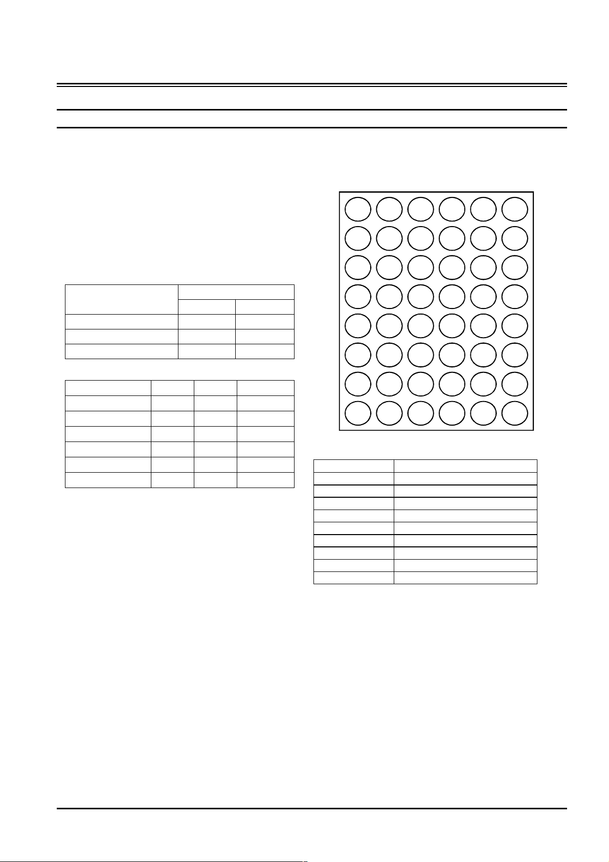
Pin Assignment
48-Ball BGA (CSP), Top View
123456
A
B
C
D
E
F
G
H
LB# OE# A0 A1 A2 CE2
DQ8 UB# A3 A4 CE1# DQ0
DQ9 DQ 10 A5 A6 DQ1 DQ 2
GND DQ11 A17 A7 DQ3 VDD
VDD DQ12 A16 DQ4 GND
DQ14 DQ13 A14 A15 DQ 5 DQ6
DQ15 NC A 12 A13 W E# DQ7
A18
GND
A8 A9 A10 A11 NC
Pin Names
Symbol Function
A0 – A18 Address Inputs
DQ0-DQ15 Data Inputs/Outputs
CE1#,CE2 Chip Enable Input
OE# Output Enable
WE# Read/Write Control Input
LB#,UB# Data Byte Control Inputs
GND Ground
V
DD
Power Supply
NC No Connection
Overview
The EM565161 is an 8M-bit SRAM organized as 512K words by 16 bits. It is designed with advanced CMOS
technology. This Device operates from a single power supply. Advanced circuit technology provides both high
speed and low power. It is automatically placed in low-power mode when CE1# or both UB# and LB# are
asserted high or CE2 is asserted low. There are three control inputs. CE1# and CE2 are used to select the
device and for data retention control, and output enable (OE#) provides fast memor y access. Data byte control
pin (LB#,UB#) provides lower and upper byte access. This device is well suited to various microprocessor
system applications where high speed, low power and battery backup are required. And, with a guaranteed
operating range from –40°C to 85°C, the EM565161 can be used in environments exhibiting extreme
temperature conditions.
Etron Technology, Inc.
No. 6, Technology Rd. V, Science-Based Industrial Park, Hsinchu, Taiwan 30077, R.O.C.
TEL: (886)-3-5782345 FAX: (886)-3-5778671
Etron Technology, Inc., reserves the right to make changes to its products and specifications without notice.
Page 2
Etr onT ech
Block Diagram
EM565161
DQ0
DQ1
DQ2
DQ3
DQ4
DQ5
DQ6
DQ7
DQ8
DQ9
DQ10
DQ11
DQ12
DQ13
DQ14
DQ15
A0
A18
MEMORY
CELL ARRAY
512kx16
SENSE AMP
COLUMN ADDRESS
DECODER
VDD
GND
WE#
UB#
LB#
OE#
CE1#
CE2
POWER DO WN
CIRCUIT
Preliminary 2 Rev 0.9 Jan 2002
Page 3
Etr onT ech
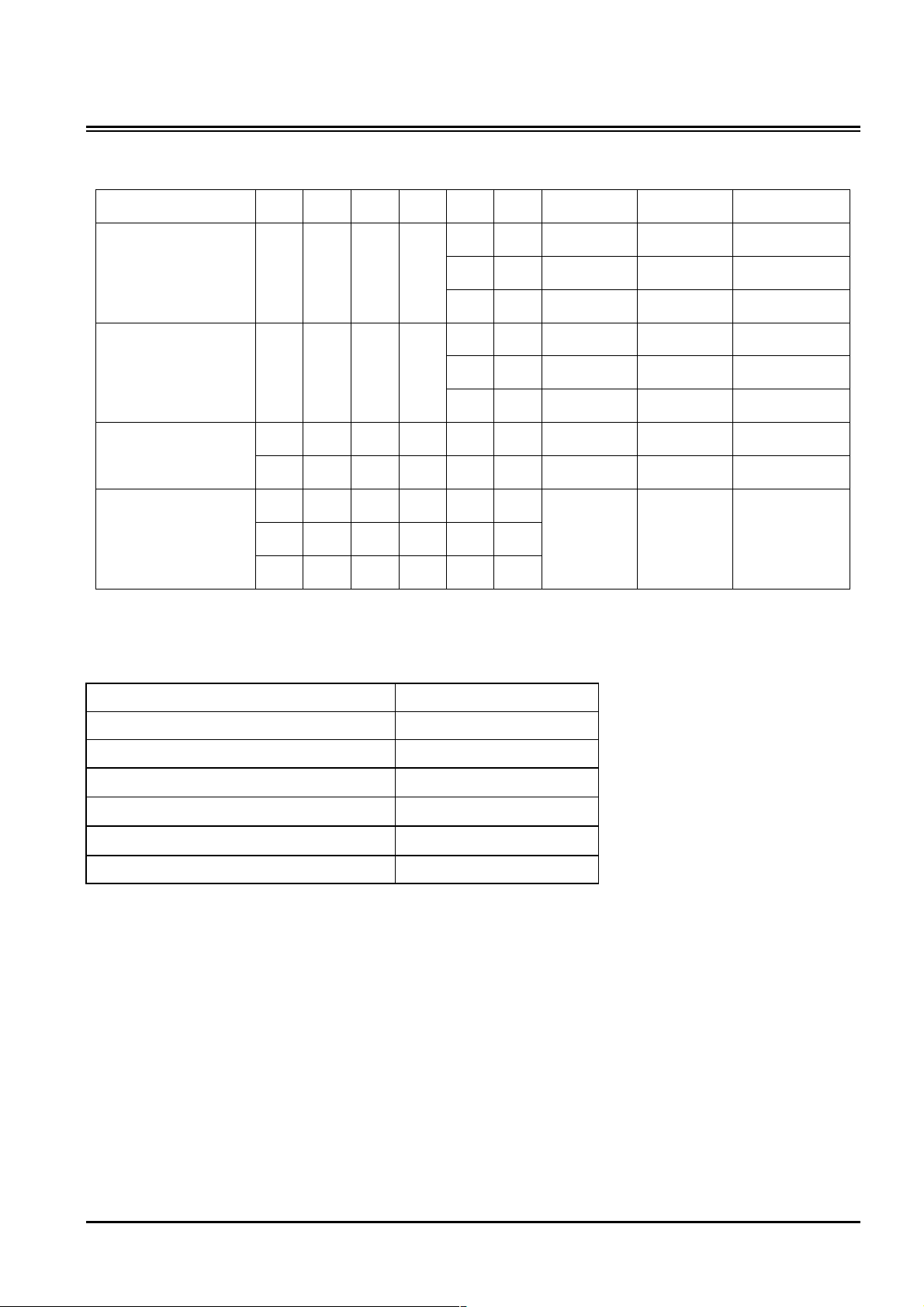
Operating Mode
Mode CE1# CE2 OE# WE# LB# UB# DQ0~DQ7 DQ8~DQ15 Power
EM565161
Read L H L H
Write L H X L
L H H H X X High-Z High-Z I
Output Disabled
L H X X H H High-Z High-Z I
H X X X X X
Standby
X L X X X X
X X X X H H
Note:X=don’t care. H=logic high. L=logic low.
Absolute Maximum Ratings
L L D
H L High-Z D
L H D
L L DIN D
H L High-Z DIN I
L H DIN High-Z I
D
OUT
High-Z I
OUT
High-Z High-Z I
I
OUT
I
OUT
I
IN
DDO
DDO
DDO
DDO
DDO
DDO
DDO
DDO
DDS
Supply voltage, VDD -0.3 to +4.6V
Input voltages, VIN -0.3 to +4.6V
Input and output voltages, V
Operating temperature, T
Storage temperature, T
Soldering Temperature (10s), T
Power dissipation, PD 1 W
STRG
-0.5 to VDD +0.5V
I/O
OPR
SOLDER
-40 to +85°C
-55 to +150°C
240°C
Preliminary 3 Rev 0.9 Jan 2002
Page 4
Etr onT ech
EM565161
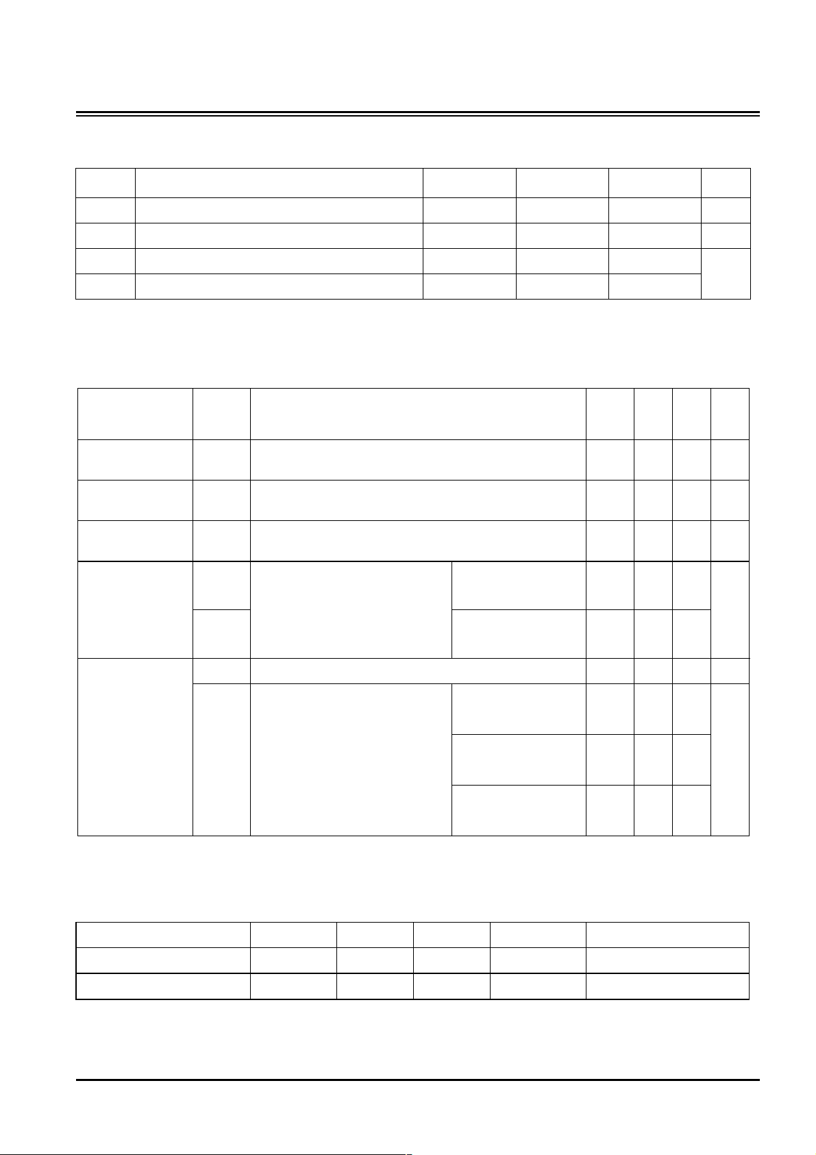
DC Recommended Operating Conditions (Ta=-40°C to 85°C)
Symbol Parameter Min Typ Max Unit
VDD Power Supply Voltage 2.3 3.0 3.6 V
VIH Input High Voltage 2.2
VIL Input Low Voltage -0.3
VDR Data Retention Supply Voltage 1.0
Note:
(1) Overshoot : VDD +2.0V in case of pulse width ≤ 20ns
(2) Undershoot : -2.0V in case of pulse width ≤ 20ns
(2)
−
−
−
V
DD
+ 0.3
0.6
3.6
(1)
DC Characteristics (Ta = -40°C to 85°C, VDD = 2.3V to 3.6V)
Parameter Symbol Test Conditions Min Typ* Max Unit
Input low current IIL I
Output low
voltage
Output high
voltage
Operating current I
I
Standby current I
I
-55E/70E
Notes:
* Typical value are measured at T
VOL I
VOH I
DD1
DD2
DDS1
DDS2
= 0V to VDD - 1
IN
= 2.1 mA
OL
= -1.0 mA
OH
CE1# = V
CE2 = V
I
= 0mA
OUT
Other Input = V
CE1# = V
CE1# = V
UB# and LB# = VDD-0.2V or
CE2 = 0.2V
= 25°C.
a
and
IL
and
IH
or CE2 = VIL
IH
DD
Capacitance (Ta = 25°C; f = 1 MHz)
/ VIL
IH
– 0.2V or
Cycle time = min
Cycle time = 1µs
-55
-70
V
DD
0.15
−
−
−
−
−
−
−
−
−
–
−
12 35
−
−
2 35
2 25
14 80
1
µ
A
0.4 V
V
−
mA
5
0.3 mA
µ
A
Parameter Symbol Min Max Unit Test Conditions
Input capacitance CIN
Input/Output capacitance CIO
Notes:
This parameter is periodically sampled and is not 100% tested.
−
−
8 pF VIN = GND
10 pF VIO = GND
Preliminary 4 Rev 0.9 Jan 2002
Page 5

Etr onT ech
EM565161
AC Characteristics and Operating Conditions (Ta = -40°C to 85°C, VDD = 2.3V to 3.6V)
Read Cycle
EM565161
Symbol Parameter
-55 -70
Min Max Min Max
Unit
tRC Read cycle time 55
tAA Address access time
t
Chip Enable (CE1#) Access Time
CO1
t
Chip Enable (CE2) Access Time
CO2
tOE Output enable access time
tBA Data Byte Control Access Time
tLZ Chip Enable Low to Output in Low-Z 10
t
Output enable Low to Output in Low-Z 5
OLZ
t
Data Byte Control Low to Output in Low-Z 10
BLZ
tHZ Chip Enable High to Output in High-Z
t
Output Enable High to Output in High-Z
OHZ
t
Data Byte Control High to Output in High-Z
BHZ
tOH Output Data Hold Time 10
Write Cycle
Symbol Parameter
70
−
55
−
55
−
55
−
25
−
55
−
−
−
−
20
−
20
−
20
−
−
EM565161
-55 -70
Min Max Min Max
−
−
−
−
−
10
5
10
−
−
−
10
−
70
70
70
35
70
−
−
−
25
25
25
−
ns
Unit
tWC Write cycle time 55
tWP Write pulse width 45
tCW Chip Enable to end of write 45
tBW Data Byte Control to end of Write 45
tAS Address setup time 0
tWR Write Recovery time 0
t
WE# Low to Output in High-Z
WHZ
tOW WE# High to Output in Low-Z 5
tDS Data Setup Time 25
tDH Data Hold Time 0
AC Test Condition
Output load : 60pF + one TTL gate
•
Input pulse level : 0.4V, 2.4V
•
Timing measurements : 0.5 x V
•
tR, tF : 5ns
•
DD
70
−
−
−
−
−
−
20
−
−
−
−
55
60
60
0
0
−
5
30
0
−
−
−
−
−
ns
−
20
−
−
−
Preliminary 5 Rev 0.9 Jan 2002
Page 6

Etr onT ech
Read Cycle
(See Note 1)
Address
t
RC
EM565161
CE1#
CE2
OE#
t
AA
t
CO1
t
CO2
t
OE
t
HZ
t
OH
t
OHZ
t
BA
UB# LB#
,
t
D
OUT
t
LZ
t
OLZ
BLZ
V AL ID D A TA O U T
t
BHZ
Preliminary 6 Rev 0.9 Jan 2002
Page 7

Etr onT ech
Write Cycle1
(WE# Controlled)(See Note 4)
Address
t
WC
EM565161
WE#
CE1#
CE2
UB# LB#
,
t
AS
t
WHZ
t
CW
t
CW
t
BW
t
WP
t
WR
t
OW
D
D
OUT
IN
(See Note2) (See Note3)
(See N ote 5)
t
DS
VA LID DA TA IN (See N ote 5)
t
DH
Preliminary 7 Rev 0.9 Jan 2002
Page 8

Etr onT ech
Write Cycle 2
(CE1# Controlled)(See Note 4)
Address
t
WC
EM565161
WE#
CE1#
CE2
UB# LB#
,
t
AS
t
BLZ
t
WHZ
t
CW
t
CW
t
BW
t
WP
t
WR
D
OUT
t
LZ
t
DS
D
IN
(See N ote 5) VA LID DA TA IN
t
DH
Preliminary 8 Rev 0.9 Jan 2002
Page 9

Etr onT ech
Write Cycle 3
(CE2 Controlled)(See Note 4)
Address
t
WC
EM565161
WE#
CE1#
CE2
D
OUT
t
AS
t
LZ
t
WHZ
t
CW
t
CW
t
WP
t
DS
t
WR
t
DH
D
IN
(See N ote 5) VA LID DA TA IN
Preliminary 9 Rev 0.9 Jan 2002
Page 10

Etr onT ech
Write Cycle4
(UB#, LB# Controlled)(See Note 4)
Address
t
WC
EM565161
WE#
CE1#
CE2
UB# LB#
,
t
AS
t
BLZ
t
WHZ
t
CW
t
CW
t
BW
t
WP
t
WR
D
OUT
t
LZ
t
DS
D
IN
(See N ote 5) VA LID DA TA IN
t
DH
Note:
1. WE# remains HIGH for the read cycle.
2. If CE1# goes LOW (or CE2 goes HIGH) with or after WE# goes LOW, the outputs will remain at high
impedance.
3. If CE1# goes HIGH (or CE2 goes LO W) coincident with or before WE# goes HIGH, the outputs will remain at
high impedance.
4. If OE# is HIGH during the write cycle, the outputs will remain at high impedance.
5. Because I/O signals may be in the output state at this time, input signals of reverse polarity must not be
applied.
Preliminary 10 Rev 0.9 Jan 2002
Page 11

Etr onT ech
EM565161
Data Retention Characteristics (Ta = -40°C to 85°C)
Symbol Parameter Min Typ Max Unit
CE1# ≥ V
VDR
Data Retention Supply
Voltage
or UB# = LB# ≥ V
or CE2 ≤ 0.2V,
VIN ≥ V
t
Chip Deselect to Data Retention Mode Time 0
SDR
t
Recovery Time tRC
RDR
– 0.2V
DD
– 0.2V
DD
– 0.2V or VIN ≤ 0.2V
DD
CE1# or UB#/LB# Controlled Data Retention Mode
Data Retention Mode
N ote 1
V
DD
2.7V
2.2V
V
DR
CE1#,
UB#/LB#
GND
t
SDR
CE2 Controlled Data Retention Mode
V
DD
Data Reten tion Mode
1.0
t
RDR
3.6 V
−
−
−
−
−
ns
ns
2.7V
CE2
V
DR
0.4V
GND
t
SDR
Note:
1. CE1# ≥ VDD – 0.2V or UB# = LB# ≥ VDD – 0.2V
2. CE2 ≤ 0.2V
Note 2
t
RDR
Preliminary 11 Rev 0.9 Jan 2002
Page 12

Etr onT ech
Package Diagrams
48-Ball (8mm x 10mm) BGA
Units in mm
TOP VIEW
EM565161
BOTTOM VIEW
PIN 1 CORNER
A
B
C
D
E
F
G
H
123456
10 .0 0.1
5
2
5.
5
7
0.
0.10
S C
0.25
S
0.30 0.05(4 8X )
654321
PIN 1 CORNER
CAB
A
B
C
D
E
F
G
H
0.52 0.02
1.20 MA X
- C -
SEATING PLANE
0.23 0.03
0.36
0.02
0.05
- B -
0.20(4X)
D
D
- A -
0.15
0.75
3.75
8.0 0 .1
Preliminary 12 Rev 0.9 Jan 2002
Page 13

Etr onT ech
Package Diagrams
48-Ball (6mm x 9mm) BGA
Units in mm
TOP VIEW
EM565161
BOTTO M VIEW
PIN 1 CORNER
123456
L
7 8 9 10 11 12
- B -
0.10
S
0.25
S
0.30(48X)
654321
PIN 1 CORNER
C
CA B
0.75
- C - SEATING PLANE
3.75
- A -
0.20(4X)
0.10
Preliminary 13 Rev 0.9 Jan 2002
 Loading...