

Page 1
16 DIGIT LCD DRIVER WITH CHECK TIME FUNCTION
Preliminary
GENERAL DESCRIPTION
EM32117 is a CMOS 16-digit LCD panel driver. The EM32117 can receive dialing information such as dialing
digits, Pause, Flash, Pulse to Tone mode from EMC EM91465 series dialer IC and display the corresponding
pattern on the LCD panel. The EM32117 also supports various indicators such as the icons of STORE, SAVE,
Speaker phone (or Hand-Free), Lower or Upper page, Hold, etc. to support high-end feature phone applications.
The EM32117 can operate in stand-alone mode to display calendar and real time clock, conversation time
(stopwatch). The EM32117 also provides check the last conversation time function.
FEATURES
• ON-HOOK check last conversation time function.
• General flag display function for LOGO indication.
• Low power consumption: 1.5µA (max.)
• Uses single clock 32768 Hz crystal (with built-in capacitor, no need extra capacitor).
• LCD blank 2 sec after OFF-HOOK, to protect the STW data.
• Built-in serial data interface (compatiable with EM91465 series).
• Driver for 4.5-volt, 16-digit, 1/4 duty , 1/3 bias LCD panel with built-in voltage tripler circuit.
• Display dialing phone number.
• Display calendar and real time clock (RTC) in 12 hour or 24 hour format.
• Stopwatch function for counting conversation time up to 59 minutes 59 seconds.
• Operating voltage: 1.5 VDC ( typical )
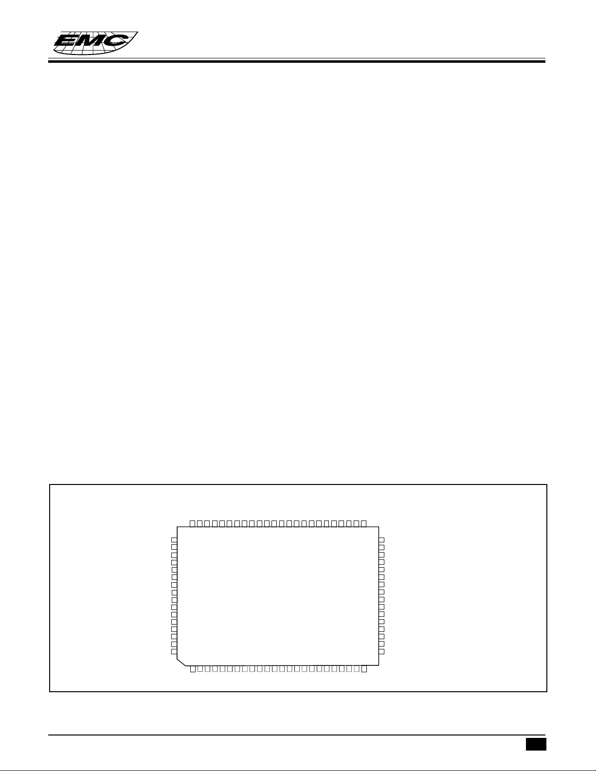
• Dice form, QFP 80 pin package, and LCM (Liquid Crystal display Module) are available.
EM32117
APPLICATION
• LCD Feature phone and Digital display system.
PIN ASSIGMENT
NCNCNCNCNCNCSEG26
SEG25
SEG24
SEG23
SEG22
SEG21
SEG20
SEG19
SEG18
SEG17
SEG16
SEG15
SEG14
SEG13
SEG12
SEG11
SEG10
6463626160595857565554535251504948474645444342
65
66
67
68
69
70
71
72
73
74
75
76
77
78
79
80
123456789
NCNCNCNCNCNCNC
SEG27
SEG28
SEG29
SEG30
SEG31
COM0
COM1
COM2
COM3
ENCLND*
ENRTC*
24/12*NCNCNCNC
EM32117Q
101112131415161718192021222324
SEG9
SEG8
SEG7
SEG6
SEG5
SEG4
SEG3
SEG2
SEG1
SEG0GFTEST
NC
41
NCNCNCNCNC
XOUT
40
XIN
39
SS
V
38
VC2
37
VC1
36
V3
35
V2
34
V
DD
33
HKS
32
SD1
31
MS2
30
MS1
29
SPARE1
28
SPARE2
27
NC
26
NC
25
* This specification are subject to be changed without notice.
3.17.1999
1
Page 2
EM32117
16 DIGIT LCD DRIVER WITH CHECK TIME FUNCTION
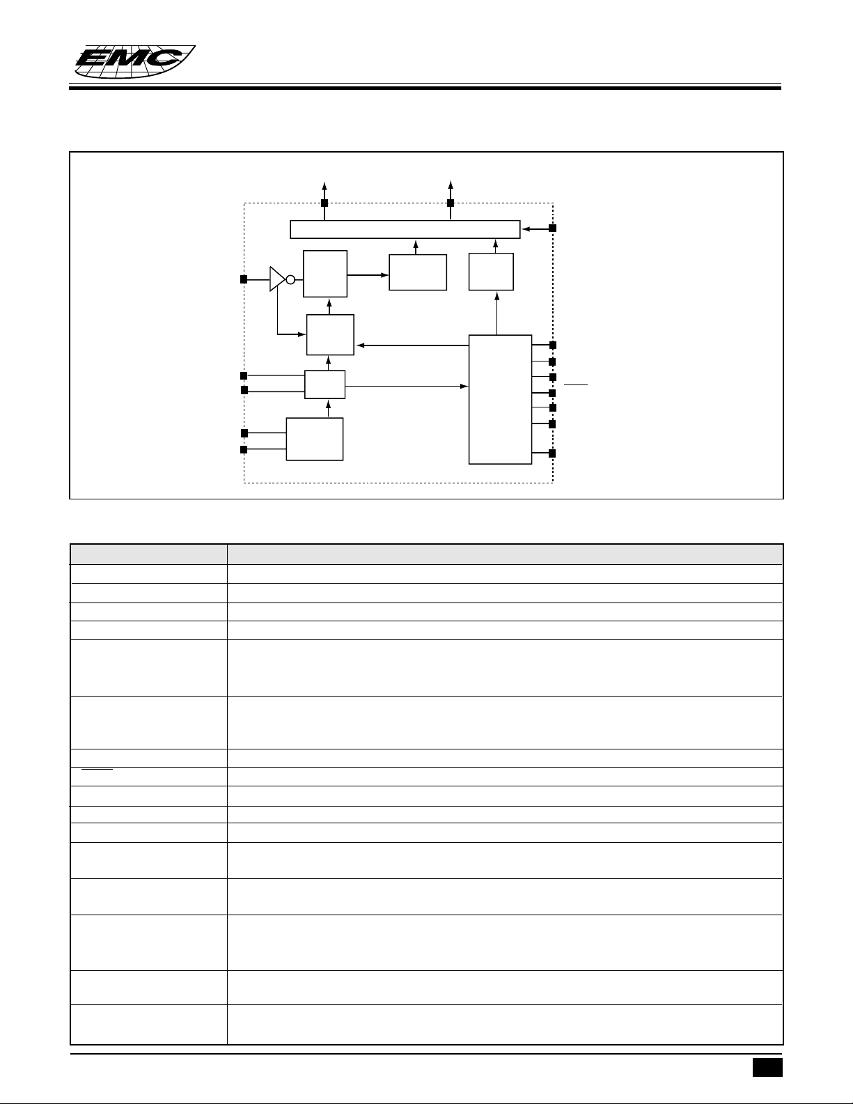
FUNCTION BLOCK DIAGRAM
SD1
XIN
XOUT
VDD
VSS
Preliminary
COM0~3
1/4 Duty 1/3 bias LCD Driver
Serial Data
Sampling
&
Decoding
Sampling
Signal
Generator
OSC
Power
Supply
Circuit
Serial Data
Display Buffer
SEG0~31
RTC/STW
Counter
Timing
Control
Circuit
GF
ENCLND
ENRTC
&
24/12
HKS
MS2
MS1
TEST
PIN DESCRIPTION
Pin Name Description
SPARE1, SPARE2 Need to be connected to V
COM0~COM3 LCD panel driver common output pins.
SEG0~SEG31 LCD panel driver segment output pins.
TEST Reserved for testing, should be left open.
MS1 Manual setting and check last conversation time input pin 1, with built-in pull-up optimal
resistor. The optimal resistor before keying=100kΩ, after keying change to 1MΩ for
reducing power consumption.
MS2 Manual setting input pin 2 with built-in pull-up; optimal resistor. The
optimal resistor before keying=100kΩ, after keying change to 1MΩ for reducing power
consumption.
SDI Serial data input pin with built-in 150 KΩ pull-up resistor.
HKS Hook switch status input pin with built-in 1 MΩ pull-up resistor.
V
DD, VSS
Positive power supply pin.
V2, V3 Voltage tripler circuit for LCD driver.
VC1, VC2 Voltage tripler circuit for LCD driver.
XIN, XOUT Crystal input and output pins for connecting a 32768Hz crystal (Internal built-in 2-p
capacitor).
24/12 RTC display 24 or 12 hours format selection pin (when this pin is pulled "high, RTC will
be displayed in 24 hour format. Otherwise will be display in 12 hour format).
ENCLND Calendar enable pin. When disabled (ENCLND* = high), the Calendar field of LCD
panel will be blanked. When 12 digit LCD panels are used, Calendar should be disable
to suppress output of calendar.
ENRTC RTC enable pin. When disabled (ENRTC* = high), the LCD panel will be blanked when
HKS pin is at high level.
GF General Flag input pin without built-in resistor. When GF pull "High" LCD panel will
display Icon. GF pull "Low", "GF" Icon will blank.
.
SS
* This specification are subject to be changed without notice. 3.17.1999
2
Page 3

16 DIGIT LCD DRIVER WITH CHECK TIME FUNCTION
Preliminary
LCD Panel Description
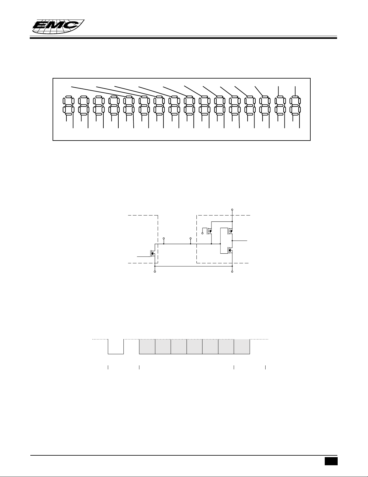
The display font of the EM32117 LCD driver is shown as the following:
Digit #
141516 1
111213
EM32117
4
5678910
23
MEMORYRD
SPEAKER
BLANK DASH
HOLD AUTO LOCK SAVE MUTE
LO BATT ALARM
54
STORE
PAGE
*
0
987321 6
PAUSE
#
TONE
SEG31 SEG30 SEG29 SEG28 SEG27 SEG26 SEG25 SEG24
COM3 16f 16a 15f 15a 14f 14a 13f 13a
COM2 16g 16b 15g 15b 14g 14b 13g 13b
COM1 16e 16c 15e 15c 14e 14c 13e 13c
COM0 16d 15d 14d 13d
SEG23 SEG22 SEG21 SEG20 SEG19 SEG18 SEG17 SEG16
COM3 12f 12a 11f 11a 10f 10a 9f 9a
COM2 12g 12b 11g 11b 10g 1b 9g 9b
COM1 12e 12c 11e 11c 10e 10c 9e 9c
COM0 12d RD 11d Speaker 10d HOLD 9 d Memory
SEG15 SEG14 SEG13 SEG12 SEG11 SEG10 SEG9 SEG8
COM3 8f 8a 7f 7a 6f 6a 5f 5a
COM2 8g 8b 7g 7b 6g 6b 5g 5b
COM1 8e 8c 7e 7c 6e 6c 5e 5c
COM0 8d GF 7d ALARM 6d STORE 5d PAGE
SEG7 SEG6 SEG5 SEG4 SEG3 SEG2 SEG1 SEG0
COM3 4f 4a 3f 3a 2f 2a 1f 1a
COM2 4g 4b 3g 3b 2g 2b 1g 1b
COM1 4e 4c 3e 3c 2e 2c 1e 1c
COM0 4d AUTO 3 d LOCK 2d SAVE 1d MUTE
GF
ALARM PAGESTOREMEMORYRD SPEAKER HOLD AUTO LOCK SAVE MUTE
COM3
COM2
COM1
COM0
* This specification are subject to be changed without notice.
3.17.1999
3
Page 4
16 DIGIT LCD DRIVER WITH CHECK TIME FUNCTION
Preliminary
EM32117
SEG31
SEG29
SEG30
SPEAKER
SEG27
SEG28
MEMORYRD
HOLD AUTO LOCK SAVE MUTE
SEG25
SEG23
SEG21
SEG26
SEG24
SEG22
SEG20
GF
SEG19
SEG17
SEG18
ALARM
SEG16
STORE
SEG15
SEG14
SEG13
PAGE
SEG11
SEG12
SEG10
SEG9
SEG8
SEG7
SEG6
SEG5
SEG4
SEG3
SEG2
SEG1
SEG0
Figure 2 - Segment pin wiring diagram
Serial Data Interface
Since the serial data transmitters (e.g. EM91465 series dialers) may have different voltage level from EM32117,
therefore the following interconnecting scheme is recommended when using the EM32117 as a serial data
receiver. The SDO output from the serial data transmitters should be of NMOS open-drain structure as shown
below.
Dialer
EM32117
546
SDO SDI
1
2
3
Vss
VCC
546
2
1
3
VssVss
Data Format
When the EM32117 senses the falling edge of the Start bit, it will sample subsequent bits in the middle of each
bit. The received bit will then be assembled and decoded, and corresponding pattern will be displayed on LCD
panel. The serial data format is as follows:
01 01
Start Bit
Bit 0 Bit 1 Bit 2 Bit 3 Bit 4 Bit 5
Data Bits
Stop Bit
Protocol
There are three categories of dialing data, and representation and interpretation of serial data is as the following:
(Note: Codes 0000 and 1111 will be interpreted as" " (blank pattern) and"-"patterns, respectively and they
will shift on LCD panel just as other digit codes.
* This specification are subject to be changed without notice. 3.17.1999
4
Page 5
Preliminary
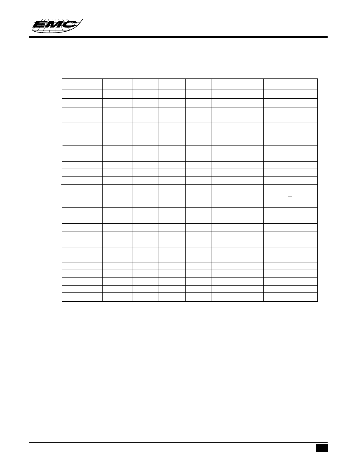
∗ Keypad,SDO format and LCD display reference table:
Keypad bit5 bit4 bit3 bit2 bit1 bit0 Display
1000001 1
2000010 2
3000011 3
4000100 4
5000101 5
6000110 6
7000111 7
8001000 8
9001001 9
0001010 0
"*"/T 0 0 1 0 1 1
#001100
P001101 P
*/"T" 0 0 1 1 1 0
ST 1 0 0 0 0 0 STORE
HOLD 1 0 1 0 0 0 HOLD
HF 1 0 1 0 1 0 Speaker
Page 1 0 1 1 0 0 PAGE
A101110 A
F 1 0 1 1 1 1 clear all display
(Lock state) 1 0 0 0 0 1 Lock
MUTE 1 0 0 0 1 0 MUTE
Note 3 1 0 0 0 1 1 ALARM
EM1~EM3 1 1 1 1 0 0 MEMORY
M1~M40 1 1 1 1 0 0 MEMORY
RD 1 1 1 1 0 1 RD
SAVE 1 1 1 1 1 0 SAVE
Note:
1. Flash key will be treated as "clear LCD panel" command.
2. When lock condition establish.
3. MUTE and ALARM indicators will toggle with each received SDI code.
4. Any invalid data will be ignored by the EM32117.
• General flag display function. EM32117 provide General Flag Icon, when GF pin pull "high", then "GF" Icon
will be displayed. GF pin pull "low", the "GF" Icon will blank. The "GF" Icon can identify by user for special
distinguishment.
EM32117
16 DIGIT LCD DRIVER WITH CHECK TIME FUNCTION
FUNCTION DESCRIPTION
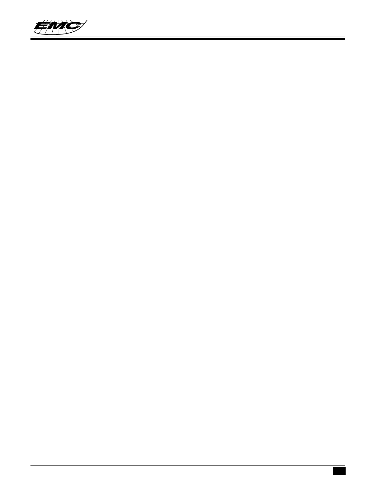
Operation Modes and System States
Depending on which state the EM32117 is in, the system will operate in one of two modes, namely, RTC mode
and Stop-watch mode. In the State 1, as defined by the State-diagram in figure 4, the system operates in RealTime Clock mode, otherwise, the system operates in Stop-Watch mode. The flow chart is as follows:
* This specification are subject to be changed without notice.
3.17.1999
5
Page 6
16 DIGIT LCD DRIVER WITH CHECK TIME FUNCTION
Preliminary
EM32117
1
RTC Mode
State>1
State=1
2
Stop watch
Mode
Figure 3 - Top Level Flow Chart
The system can be in one of the six states as defined by the following state diagram. The transitions between
states are driven by the level of HKS pins as well as Serial Data "Hand-Free" and "Hold".
HKS=Lo
HKS=Hi
HF
HF
2
Off-hook state
HD
HD
HF
4
On-hook
Hand-free state
HF
HD
HF
HKS=Hi
1
On-hook state
HKS=Lo
3
Off-Hook
Hand-free state
HD
6
ON-Hook
Hold-line state
HKS=Hi
HD
HKS=Lo
HF
5
Off-Hook
Hold-line state
Figure 4 - System State Diagram
RTC (Real time clock) Mode
When the system is in State 1 and RTC function is enabled (ENRTC pin at low level), the EM32117 will be
in Real-Time Clock display mode. There are two different RTC display formats available, e.g., 12 or 24 hours
format selected by 24/12 pin. When this pin is pulled "high", RTC will be displayed in 24 hour format. When
"low", RTC will be displayed in 12 hour format, as shown in the following:
12 hour format:
24 hour format:
* This specification are subject to be changed without notice. 3.17.1999
6
Page 7
EM32117
16 DIGIT LCD DRIVER WITH CHECK TIME FUNCTION
Preliminary
Setting Calendar and Real-Time clock
When the system is in State 1(ON-HOOK idle state), the calendar and Real-Time Clock can be set up by
operating MS1 and MS2 pins as described in the following:
1. When the system is in State 1, press MS1 and hold for over 2 sec , month digits will flash,
2. Press MS2 to increment month digits.
3. Press MS1 once again, day digits will flash,
4. Press MS2 to increment day digits.
5. Press MS1 again, hour digits will flash.
6. Press MS2 to count up data.
7. Press MS1 once again, minute digits and flash,
8. Press MS2 to count up minute digits.
9. Press MS1 again to finish RTC set up, and the second digit will be reset.
Note:
1. If MS2 are pressed and hold for over 2 seconds, then data automatically count up in every 0.5 sec.
2. Digit flash time is 1 Hz (0.5 sec on, 0.5 sec off)
The flow chart of RTC mode is as follows:
* This specification are subject to be changed without notice.
3.17.1999
7
Page 8

RTC_MODE
RTC_Display
T
Preliminary
State>1?
F
MS1=Lo?
F
EM32117
16 DIGIT LCD DRIVER WITH CHECK TIME FUNCTION
Month flash
T
MS1=Lo
>2sec?
T
F
State>1?
F
MS1=Lo?
T
Day Flash
State>1?
F
MS1=Lo?
T
Hour flash
F
display last
conversation
time for 6 sec
F
F
MS2=Lo?
F
MS2=Lo?
N
6 sec
expired?
F
T
T
Y
Month+1
Day+1
RTC_mode
F
State>1?
F
T
F
T
Minute+1
STW_MODE
MS1=Lo?
T
Minute Flash
State>1?
F
MS1=Lo?
T
F
MS2=Lo? Hour+1
F
MS2=Lo?
Figure 5 - RTC Flow Chart
* This specification are subject to be changed without notice. 3.17.1999
8
Page 9

EM32117
16 DIGIT LCD DRIVER WITH CHECK TIME FUNCTION
Preliminary
Check last conversation time
When the system is at RTC mode, pressed MS1 less than 2 sec. The last conversation will show up on LCD screen
to check the last conversation time.
Stop Watch mode
When the system exits from State 1 (RTC mode), it will enter Stop-watch mode which is intended to count
elapsed telephone conversation time up to 59 minutes and 59 seconds and display dialing information such as
dialing number, various indicators (MEMORY, RD, HOLD, Hand-Free, etc.) For example:
• Originally the system is in State 1, and the LCD panel is in RTC display mode.
• When the HKS pin goes from "high" to "low". The LCD will be blanked.
• After 2 sec, the system switches from State 1 to State 2, the stop watch will start counting from 00-00.
• After 59 minutes and 59 seconds, the stop-watch becomes 59-59.
• Then stop-watch will wrap around and start from 00-00 again.
* This specification are subject to be changed without notice.
3.17.1999
9
Page 10

EM32117
16 DIGIT LCD DRIVER WITH CHECK TIME FUNCTION
Preliminary
Stop-Watch reset and RTC display in Stop-watch Mode
The system will enter Stop-watch mode with stop watch automatically reset when the system first switches
from State 1 to other States in the Stop-watch mode.
In addition, the stop-watch can be reset any time, e.g. when the called party answers, by pressing MS2 switch.
For example:
• 21 seconds after the system enters Stop-watch mode, the display becomes 00-21.
• When the other party answers, press MS2 key to reset the stop-watch. Then the stop-watch can reflect the
real phone conversation time.
• When the system is in Stop-watch mode, the EM32117 can be switched to RTC display by pressing MS1.
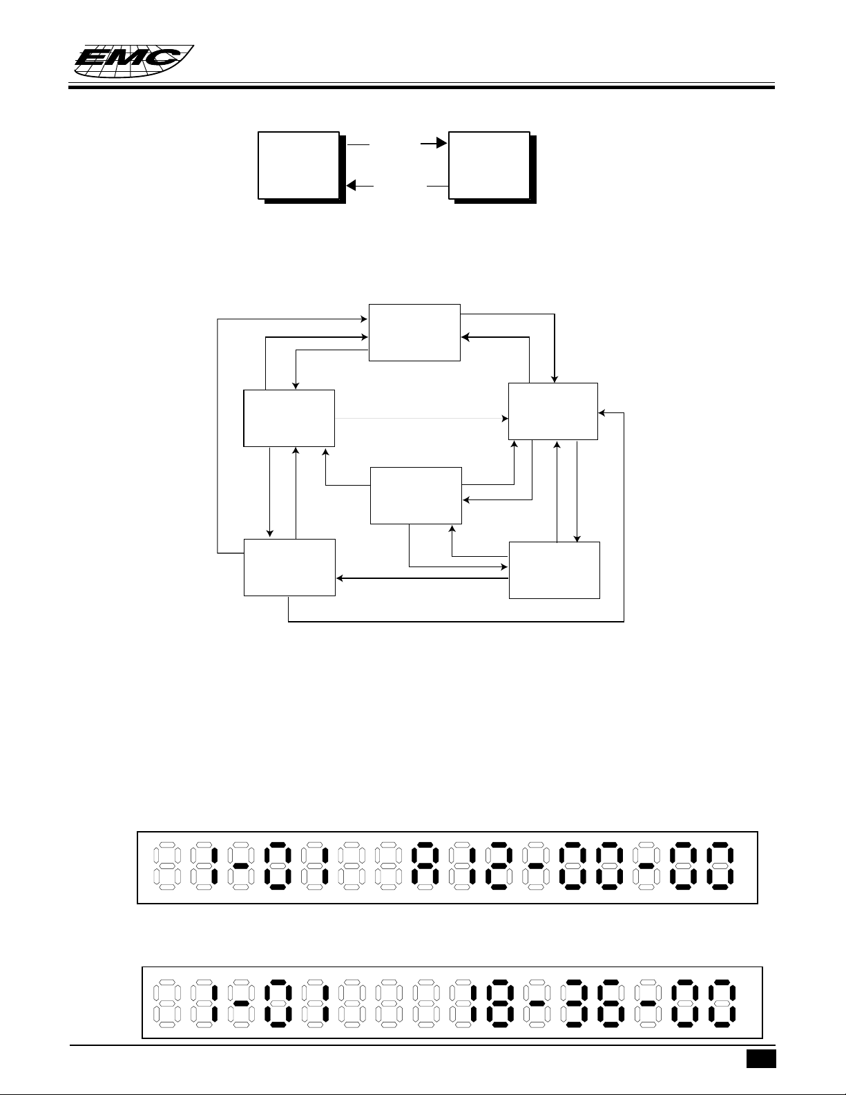
Dialing Number Display
When the system is in Stop-watch mode, each dialing digit data received from SDI pin of EM32117 will be
decoded and appears at the right most digit on LCD panel and shifts left as each subsequent digit received until
it is shifted out the panel at the left end. If no valid serial data is received for more than 6 seconds, the system
will revert to stop watch display until a new digit are received from SDI pin. Display format is as follows:
• After HKS pin goes low, the EM32117 will enter Stop-watch Mode, after 2 sec blanking state.
• When "035" are received from SDI pin, the EM32117 will switch to dialing number display.
• After "787" are received, the LCD panel is as shown below:
* This specification are subject to be changed without notice. 3.17.1999
10
Page 11

16 DIGIT LCD DRIVER WITH CHECK TIME FUNCTION
Preliminary
• Then "505" are received.
• Then "21912345" are received, the display is as follows:
EM32117
• 6 seconds after the last received digit, the EM32117 will go back to stop watch display.
.
• When the system reverts to State 1 with ENRTC* at low level, the Stop-watch will stop counting and stay on
the panel for 6 more seconds before it switches to RTC display. However, if ENRTC*is at high level when
the system returns to State 1, the LCD panel will go blank immediately.
Please refer to the following flow chart for detailed information.
Stop watch delay :
The last conversation time will prevent to be destroyed by stop watch delay function. After off-hook (or turn on
HF), STW will be displayed after 2 sec. This function is to prevent the user quickly ON-OFF HOOK to destroy
the last conversation time data.
* This specification are subject to be changed without notice.
3.17.1999
11
Page 12

STW-MODE
LCD BLANK
Reset STW
STW Display
EM32117
16 DIGIT LCD DRIVER WITH CHECK TIME FUNCTION
Preliminary
T
T
Display RTC
F
MS2 = 0?
F
MS1 = 0
T
State = 1?
State = 1?
F
Data In?
T
T
Start Timer
T
State >1?
Data Valid?
T
Display Dialing
No.
Start Timer
State = 1?
F
F
6 Sec. Expire?
RTC-MODE
F
T
RTC-MODE
F
T
T
F
F
Data in?
F
MS1 = 0?
T
F
RTC-MODE
T
Data Valid?
6 Sec. Expire?
F
T
F
F
Data In?
T
Data Valid?
T
Figure 6 - Stop-watch mode flow chart
* This specification are subject to be changed without notice. 3.17.1999
12
Page 13

EM32117
16 DIGIT LCD DRIVER WITH CHECK TIME FUNCTION
Preliminary
Displaying Indicators
When the received serial data correspond to indicators, depending on which group the indicators belong to, the
responses to the data are different.
• If the contents of the data corresponds to either one of the SPEAKER, HOLD indicators, then the states of
the indicators are governed by the state diagram in figure 4. As the state-diagram suggests, the indicators HOLD
and SPEAKER are controlled by the status of HKS pin as well as Serial Data HOLD, and SPEAKER.
Operating state HKS pin status HOLD Indicator SPEAKER Indicator
1. On-hook state Hi OFF OFF
2. Off-hook state Lo OFF OFF
3. Off-hook, HF state Lo OFF ON
4. On-hook, HF state Hi OFF ON
5. Off-hook, HD state Lo ON OFF
6. On-hook, HD state Hi ON OFF
• If the Serial Data received corresponds to one of Redial, Store, Auto, Page, Memory indicators for the first
time after HKS pin switches from high to low, it will be interpreted as "turning-on the indicator". These
indicators will remain on till 6 seconds after the last dialed number when the display mode switches from
Dialing Number Display to Stop-watch display, then these indicators will go out.
• If the received Serial Data corresponds to the codes of MUTE or ALARM, then each receptions of the same
serial data will be interpreted as "flipping (toggling) the current state of the indicator". However, when the
system returns to state 1, the MUTE will also be cleared.
Driving a 12 digit LCD panel
When the EM32117 is driving a 12 digit LCD panel, the ENCNLD should be pulled to VDD to suppress the
display of calendar. For example,
• When the system is in State 1 (the LCD panel is at RTC mode), pulling ENCNLD to VDD will disable display
of calendar.
Note: Calendar display will be automatically suppressed when Real-Time Clock is disable (pulling ENRTC
to high level).
Suppressing Real-Time Clock Display
With the ENRTC at high level (Real-Time Clock disabled) and the system is in State 1, the LCD panel will
be blanked. While the system is in Stop-watch mode, it is not possible to switch to calendar and RTC mode by
pressing MS1 key.
* This specification are subject to be changed without notice.
3.17.1999
13
Page 14

16 DIGIT LCD DRIVER WITH CHECK TIME FUNCTION
Preliminary
ABSOLUTE MAXIMUM RATINGS
Items Sym. Rating Condition
EM32117
Supply voltage V
Input voltage V
Output voltage V
DD
IN
O
- 0.5V to 5V
- 0.5V to VDD + 0.5V
- 0.5V to VDD+0.5V Except open-drain
-0.5 V to 5V Open-drain
Power dissipation P
Operating temperature T
Storage temperature T
D
OPR
STR
300 mW Topr = 50oC
0oC to 50oC
-55oC to 125oC
RECOMMENDED OPERATING CONDITIONS
1. Supply voltage at 1.5 V D.C.
2. Operation frequency fosc: 32768 Hz
3. Crystal don't need extra capacitor
DC AND AC ELECTRICAL CHARACTERISTICS (fosc=32768 Hz; V
Parameter Sym. Min. Typ. Max. Unit Condition
Operatingvoltage V
DD
V2 2VDD-0.1 2V
V3 3VDD-0.15 3V
Operating current Idd - 1 1.5 µA
(no load)
Input voltage ViH VDD-0.3 - V
(Input pins except HKS) ViL V
Input pins pull-up optimal resistor RoiH - 1 - MΩ Vi switch from VDD to
(MS1,MS2,HKS pin) RoiL - 100 - KΩ VSS and Ri switch from
SDI pin input resistance Ri - 150 - KΩ Vi = V
Oscillator frequency fosc. - 32768 - Hz
Oscillator start time Tstart - - 2 Sec. V
Common/Segment pins
HKS pin input voltage ViH V
ViL V
HKS, MS1, MS2, Tdb - 20 - mS
input pin debouce time
Crystal input and output
pin built-in capacitor C
O
1.2 1.5 1.6 V
2VDD+0.1 V
DD
3VDD+0.15
DD
SS
- 0.2V - V
DD
SS
-VSS + 0.3 V
-VSS + 0.2 V
DD
DD
-20-pF
= 1.50V)
SS
V
V
RoiL to RoiH
SS
=1.3V
DD
* This specification are subject to be changed without notice. 3.17.1999
14
Page 15

EM32117
16 DIGIT LCD DRIVER WITH CHECK TIME FUNCTION
APPLICATION CIRCUIT
1
SEG0
2
SEG1
3
SEG2
4
SEG3
5
SEG4
6
SEG5
7
SEG6
8
SEG7
9
SEG8
10
SEG9
11
SEG10
12
SEG11
13
SEG12
14
SEG13
15
SEG14
16
SEG15
17
SEG16
18
SEG17
19
SEG18
20
SEG19
21
SEG20
22
SEG21
23
SEG22
24
SEG23
LCD PANEL
SEG24
SEG25
SEG26
SEG27
SEG28
SEG29
SEG30
SEG31
COM0
COM1
COM2
COM3
25
26
27
28
29
30
31
32
33
34
35
36
Preliminary
GF
VDD
or
8
SEG3
SEG4
SEG5
SEG6
SEG7
SEG8
80
79
78
77
76
75
74
73
72
71
70
69
68
67
66
65
58
SEG9
SEG10
SEG11
SEG12
SEG13
SEG14
SEG15
SEG16
SEG17
SEG18
SEG19
SEG20
SEG21
SEG22
SEG23
SEG24
SEG25
SEG26
SEG2757SEG2856SEG2955SEG3054SEG3153COM052COM151COM250COM3
EM32117
SEG2
49
18
SEG0
SEG1
ENCLND48ENRTC4724/12
GF
TEST
SPARE2
SPARE1
XOUT
46
MS1
MS2
SDI
HKS
VDD
VC1
VC2
VSS
XIN
27
28
29
30
31
32
33
34
V2
35
V3
36
37
38
39
40
19
17
16
15
14
13
12
11
10
9
TEST
Should let it OPEN
SDI
HKS
VDD
0.1u
32768
PULL to HIGH
0.1u
MS1
MS2
0.1u
VDD
DIALER
PART VDD
1M
C945
OFF
VDD
CALENDAR
EXTRA
1.5V BATTERY
C945
C945
EM32117 can used this cricuit replace
extra battery .
RECOMMAND CRICUIT :
( But if LCD PANEL's power consumption
are too large , the extra battery still be
needed. )
ON
VDD
HKS
OFF
RTC
C945
HK
470K
1N4148
ON
VDD
24
HOUR
SDI
SDO
12
HOUR JUMP : 24/12 format select
CALENDAR JUMP : CALENDAR ON/OFF
MS1 ,MS2 adjust Time
RTC JUMP : Real Time Clock ON/OFF
GF JUMP : General Flag icon for LOGO ON/OFF
NOTED :
* This specification are subject to be changed without notice.
3.17.1999
15
Page 16

EM32117
16 DIGIT LCD DRIVER WITH CHECK TIME FUNCTION
PAD DIAGRAM
SEG9
SEG8
SEG7
SEG6
SEG5
SEG4
SEG3
SEG2
SEG1
SEG0
GF
TEST
80
8
9
10
11
12
13
14
15
16
17
18
19
SEG10
79
SEG11
SEG12
78 77
27
SEG13
SEG14
76 75 74
29
28
Preliminary
SEG15
SEG16
30
SEG17
73
EM32117
3231
33
SEG18
72
(0,0)
34
SEG19
71
35
SEG20
70
36
SEG21
69
37
SEG22
68 67
38
SEG23
39
SEG24
66
40
SEG25
65
58
57
56
55
54
53
52
51
50
49
48
47
46
SEG26
SEG27
SEG28
SEG29
SEG30
SEG31
COM0
COM1
COM2
COM3
ENCLNDB
ENRTCB
F24&12B
SPARE1
SPARE2
MS1
MS2
SDI
HKS
VDD
V2
VC1
VC2
VSS
XIN
XOUT
V3
Chip Size : 2450 x 2130 µm
Pad No. Symbol X Y
8 SEG9 -1093.3 666.6
9 SEG8 -1093.3 525.5
10 SEG7 -1093.3 399.2
11 SEG6 -1093.3 258.1
12 SEG5 -1093.3 132.1
13 SEG4 -1093.3 -9.0
14 SEG3 -1093.3 -135.0
15 SEG2 -1093.3 -276.1
16 SEG1 -1093.3 -402.1
17 SEG0 -1093.3 -543.1
18 GF -1108.3 -669.1
19 TEST -1108.3 -795.1
27 SPARE2 -1083.1 -932.2
28 SPARE1 -955.0 -932.2
29 MS1 -823.4 -932.2
30 MS2 -695.3 -932.2
31 S D I -569.3 -932.2
32 H KS -437.7 -932.2
33 V
DD
-311.7 -936.1
34 V2 -185.7 -936.1
35 V3 -59.7 -940.6
36 V C 1 68.5 -936.1
* This specification are subject to be changed without notice. 3.17.1999
16
Page 17

16 DIGIT LCD DRIVER WITH CHECK TIME FUNCTION
Preliminary
Pad No. Symbol X Y
37 VC2 196.6 -941.4
38 V
39 X I N 448.6 -931.3
40 XOUT 621.6 -935.2
46 24/12 1099.3 -945.9
47 ENRTC 1099.3 -819.9
48 ENCLND 1099.3 -693.9
49 COM3 1089.8 -552.2
50 COM2 1089.8 -410.5
51 COM1 1089.8 -284.5
52 COM0 1089.8 -144.2
53 SEG31 1089.8 -18.2
54 SEG30 1089.8 122.9
55 SEG29 1089.8 248.9
56 SEG28 1089.8 390.0
57 SEG27 1089.8 516.0
58 SEG26 1089.8 657.1
65 SEG25 1081.7 929.6
66 SEG24 929.5 929.6
67 SEG23 788.3 929.6
68 SEG22 661.3 929.6
69 SEG21 520.2 929.6
70 SEG20 380.2 929.6
71 SEG19 210.6 929.6
72 SEG18 72.3 929.6
73 SEG17 -83.5 929.6
74 SEG16 -221.8 929.6
75 SEG15 -377.6 929.6
76 SEG14 -512.5 929.6
77 SEG13 -660.6 929.6
78 SEG12 -788.4 929.6
79 SEG11 -929.5 929.6
80 SEG10 -1085.4 929.6
SS
322.6 -931.3
EM32117
* This specification are subject to be changed without notice.
3.17.1999
17
Page 18

16 DIGIT LCD DRIVER WITH CHECK TIME FUNCTION
Preliminary
12 DIGITS LCD PANEL DESIGN NOTE
LCD Panel Description
The 12 digits LCD display font of the EM32117 LCD driver is shown as the following :
Digit #
4
141516 1
111213
5678910
23
EM32117
SPEAKER
MEMORYRD
HOLD AUTO LOCK SAVE MUTE
LO BATT ALARM
54
STORE
PAGE
*
0
9876
PAUSE
#
TONE
DASH
SEG23 SEG22 SEG21 SEG20 SEG19 SEG18 SEG17 SEG16
COM3 12f 12a 11f 11a 10f 10a 9f 9a
COM2 12g 12b 11g 11b 10g 1b 9g 9b
COM1 12e 12c 11e 11c 10e 10c 9e 9c
COM0 12d RD 11d Speaker 10d HOLD 9d Memory
SEG15 SEG14 SEG13 SEG12 SEG11 SEG10 SEG9 SEG8
COM3 8f 8a 7f 7a 6f 6a 5f 5a
COM2 8g 8b 7g 7b 6g 6b 5g 5b
COM1 8e 8c 7e 7c 6e 6c 5e 5c
COM0 8d GF 7d ALARM 6d STORE 5d PAGE
SEG7 SEG6 SEG5 SEG4 SEG3 SEG2 SEG1 SEG0
COM3 4f 4a 3f 3a 2f 2a 1f 1a
COM2 4g 4b 3g 3b 2g 2b 1g 1b
COM1 4e 4c 3e 3c 2e 2c 1e 1c
COM0 4d AUTO 3d LOCK 2d SAVE 1d MUTE
GF
ALARM PAGESTOREMEMORYRD SPEAKER HOLD AUTO LOCK SAVE MUTE
COM3
COM2
COM1
COM0
* This specification are subject to be changed without notice. 3.17.1999
18
Page 19

16 DIGIT LCD DRIVER WITH CHECK TIME FUNCTION
Preliminary
EM32117
SPEAKER
RD HOLD AUTO LOCK SAVE MUTE
SEG23
MEMORY
SEG21
SEG22
SEG20
SEG19
GF
SEG17
SEG18
SEG15
SEG16
STOREALARM
SEG13
SEG14
PAGE
SEG11
SEG12
SEG10
SEG9
SEG8
SEG7
SEG6
SEG5
SEG4
SEG3
SEG2
SEG1
SEG0
Figure 2 - Segment pin wiring diagram
Driving a 12 digit LCD panel
When the EM32117 is driving a 12 digit LCD panel, the ENCNLD should be pulled to VDD to suppress the
display of calendar. For example,
• When the system is in State 1 (the LCD panel is at RTC mode), pulling ENCNLD to VDD will disable display
of calendar.
Note: Calendar display will be automatically suppressed when Real-Time Clock is disable (pulling ENRTC
to high level).
* This specification are subject to be changed without notice.
3.17.1999
19
Page 20

EM32117
16 DIGIT LCD DRIVER WITH CHECK TIME FUNCTION
PAD DIAGRAM
SEG9
SEG8
SEG7
SEG6
SEG5
SEG4
SEG3
SEG2
SEG1
SEG0
GF
TEST
80
8
9
10
11
12
13
14
15
16
17
18
19
SEG10
79
SEG11
SEG12
78 77
27
SEG13
28
SPARE1
SPARE2
Preliminary
SEG14
SEG15
SEG16
SEG17
SEG18
72
30
MS2
73
(0,0)
EM32117
33
3231
SDI
HKS
VDD
34
76 75 74
29
MS1
V2
SEG19
71
35
V3
SEG20
70
36
VC1
69
37
VC2
SEG21
SEG22
68 67
38
VSS
SEG23NCNC
66
39
40
XIN
XOUT
65
48
47
58
57
56
55
54
53
52
51
50
49
46
NC
NC
NC
NC
NC
NC
COM0
COM1
COM2
COM3
ENCLNDB
ENRTCB
F24&12B
Chip Size : 2450 x 2130 µm
Pad No. Symbol X Y
8 SEG9 -1093.3 666.6
9 SEG8 -1093.3 525.5
10 SEG7 -1093.3 399.2
11 SEG6 -1093.3 258.1
12 SEG5 -1093.3 132.1
13 SEG4 -1093.3 -9.0
14 SEG3 -1093.3 -135.0
15 SEG2 -1093.3 -276.1
16 SEG1 -1093.3 -402.1
17 SEG0 -1093.3 -543.1
18 GF -1108.3 -669.1
19 TEST -1108.3 -795.1
27 SPARE2 -1083.1 -932.2
28 SPARE1 -955.0 -932.2
29 MS1 -823.4 -932.2
30 MS2 -695.3 -932.2
31 SDI -569.3 -932.2
32 HKS -437.7 -932.2
33 V
DD -311.7 -936.1
34 V2 -185.7 -936.1
35 V3 -59.7 -940.6
36 V C1 68.5 -936.1
* This specification are subject to be changed without notice. 3.17.1999
20
Page 21

16 DIGIT LCD DRIVER WITH CHECK TIME FUNCTION
Preliminary
Pad No. Symbol X Y
37 VC2 196.6 -941.4
38 V ss 322.6 -931.3
39 X I N 448.6 -931.3
40 XOUT 621.6 -935.2
46 24/12 1099.3 -945.9
47 ENRTC 1099.3 -819.9
48 ENCLND 1099.3 -693.9
49 COM3 1089.8 -552.2
50 COM2 1089.8 -410.5
51 COM1 1089.8 -284.5
52 COM0 1089.8 -144.2
53 NC 1089.8 -18.2
54 N C 1089.8 122.9
55 N C 1089.8 248.9
56 N C 1089.8 390.0
57 N C 1089.8 516.0
58 N C 1089.8 657.1
65 N C 1081.7 929.6
66 N C 929.5 929.6
67 SEG23 788.3 929.6
68 SEG22 661.3 929.6
69 SEG21 520.2 929.6
70 SEG20 380.2 929.6
71 SEG19 210.6 929.6
72 SEG18 72.3 929.6
73 SEG17 -83.5 929.6
74 SEG16 -221.8 929.6
75 SEG15 -377.6 929.6
76 SEG14 -512.5 929.6
77 SEG13 -660.6 929.6
78 SEG12 -788.4 929.6
79 SEG11 -929.5 929.6
80 SEG10 -1085.4 929.6
EM32117
* This specification are subject to be changed without notice.
3.17.1999
21
 Loading...