

Page 1
GENERAL DESCRIPTION
The EM32100 is a CMOS LCD display driver which can receive dialing data from dialer IC and display on
the LCD panel. The EM32100 can also display real time clock, conversation time (stopwatch).
FEATURES
• Drive 8/10 digits LCD panel.
• Display dialing number.
• Display real time clock (RTC) in 12 hour or 24 hour format selectable.
• Stopwatch function for counting conversation time up to 59 minutes 59 seconds.
• Operating voltage: 1.5 VDC ( typical )
• Operating current : 3 µA (max.)
• LCD driver method : 1/3 duty , 1/2 bias.
• Internal voltage doubler circuit for drive LCD.
• Internal dialer interface.
• Use single colck 32768Hz crystal.
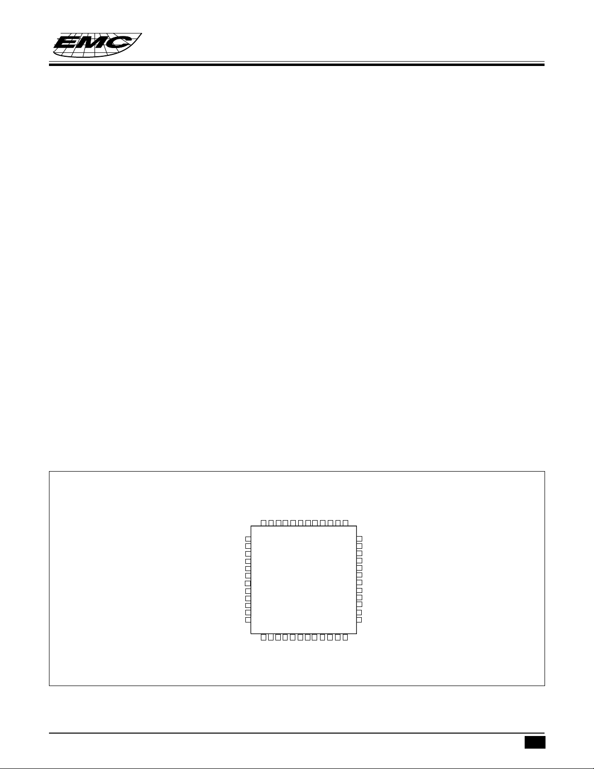
• Package in QFP 48 pins or chip form .
EM32100
EM32100
8/10 DIGIT LCD DRIVER
8/10 DIGIT LCD DRIVER
APPLICATION FIELD
Telephone and Digital display system.
PIN ASSIGNMENTS
V
SEG24
SEG23
SEG22
SEG21
SEG20
SEG19
SEG18
SEG17
NC
VP
VN
NC
ENRTC
24/12
121110
13
14
15
EE
16
17
18
19
20
21
22
23
24
2526272829303132333435
SEG16
SEG15
SEG14
VSS
XOUTNCXIN
VDDHKS
SDI
987654321
EM32100
NC
SEG9
SEG10
SEG8
SEG13
SEG12
SEG11
MS2
SEG7
MS1
48
47
46
45
44
43
42
41
40
39
38
37
36
SEG6
NC
F32H
TESTI
TEST2
COM3
COM2
COM1
SEG1
SEG2
SEG3
SEG4
SEG5
* This specification are subject to be changed without notice.
2.10.1999
1
Page 2
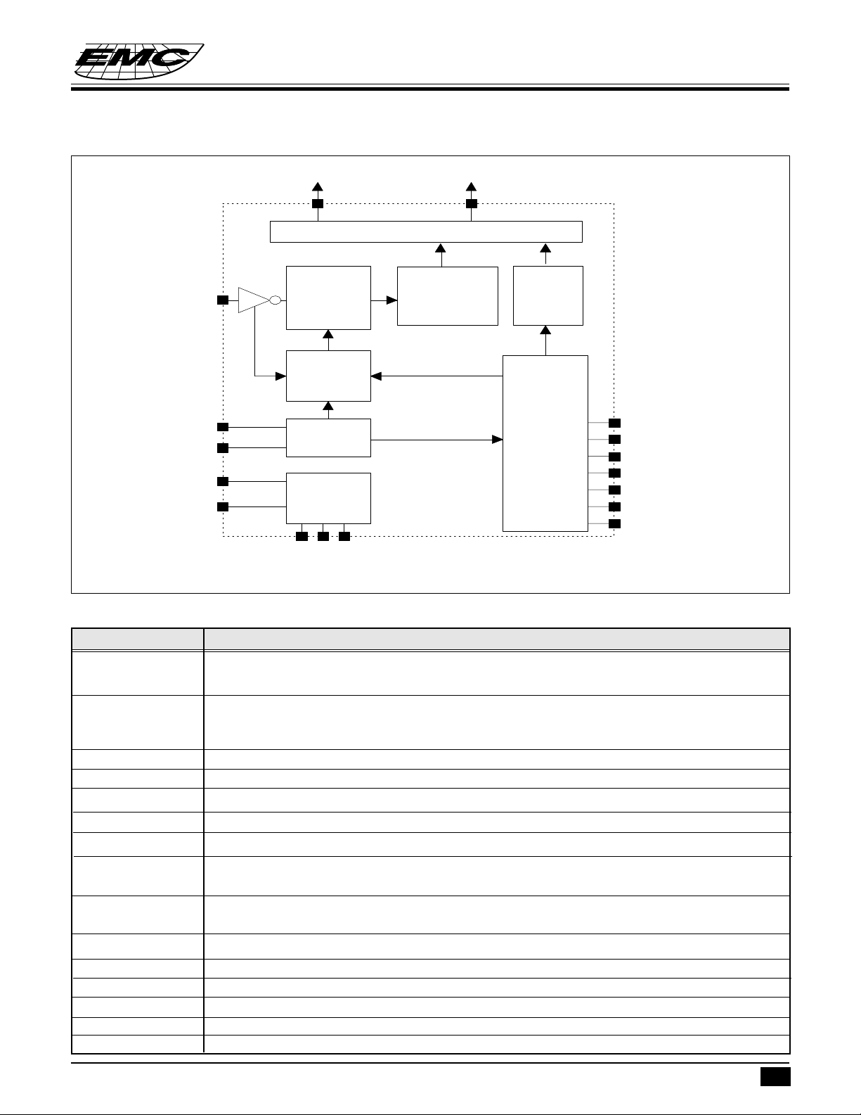
FUNCTION BLOCK DIAGRAM
EM32100
8/10 DIGIT LCD DRIVER
SDI
XIN
XOUT
VDD
VSS
COM1~3
1/3 Duty 1/2 Bias LCD Driver
Serial
Data
Samplin
Decoding
Sampling
Signal
Generator
OSC.
Power
Supply
Circuit
VP
VEE
&
VN
Serial
Display
SEG1~24
Data
Buffer
RTC/STW
Counter
Timing
&
Control
Circuit
ENRTC*
24/12
HKS*
*
MS2
MS1
F32HZ
TESTI*
PIN DESCRIPTIONS
Symbol Function
MS1 RTC (Real Time Clock ) manual setting pin 1 (internal pull up resistor typ. 150kΩ,debounce
time=15.6ms)
MS2 RTC ( Real Time Clock ) manual setting pin 2 ; internal pull up resistor : idle ( On-Hook ) =
5MΩ , normal ( Off- Hook ) = 150kΩ ; at idle and normal state , debounce time=15.6ms ,
at test mode state , no debounce time )
SDI Serial data input pin ( internal pull up resistor = 5 MΩ)
HKS Hook switch status input pin. ( This pin "High",On-Hook ; "Low",Off-Hook )
V
DD
XIN,XOUT Crystal input and output pins(crystal=32768Hz)
V
SS
24/12 RTC display 24 or 12 hours format select pin.(This pin "high",24 hours form;"low",12
ENRTC RTC enable or disable detect pin. ( This pin detect "high", RTC disable; "low" , RTC
VEE,VP,VN Voltage doubler circuit for LCD driver ( DC-DC frequency conversion=1024Hz )
SEG1~SEG24 LCD panel driver segment output pins
COM1~COM3 LCD panel driver common output pins ( Frame Frequency= 34.13 Hz).
TEST2 No connection , reserve for testing
TESTI Enter test mode detect pin
F32H Signal 32 Hz output for testing ,NMOS open drain structure
Power supply pin
Power supply pin
hours form,input pin)
enable , input pin )
* This specification are subject to be changed without notice.
2.10.1999
2
Page 3
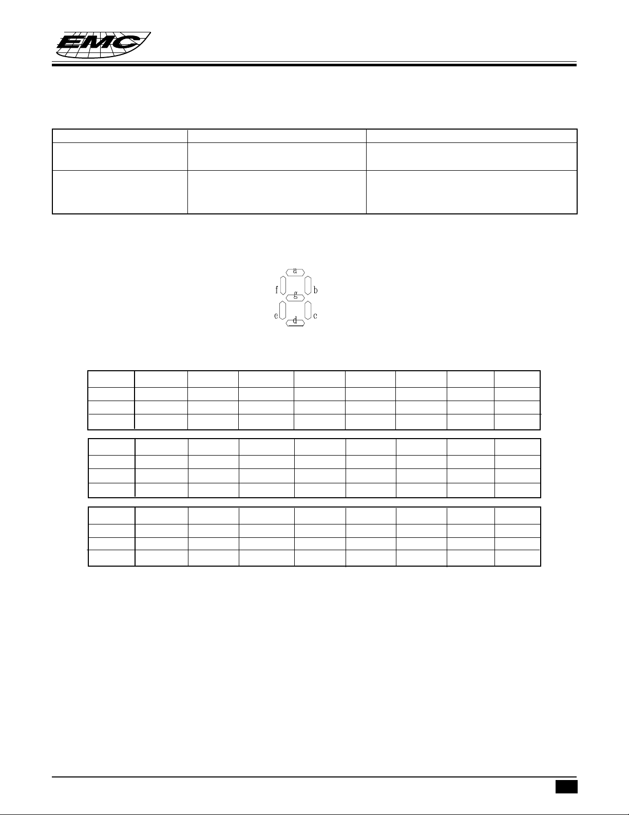
The relationship between ENRTC and EM32100 system LCD display method is as follows:
ON-HOOK (HKS="High") OFF-HOOK(HKS="Low")
ENRTC="High" blank dialing number
STW
ENRTC="Low" RTC dialing number
STW
RTC
LCD Panel Description
EM32100
8/10 DIGIT LCD DRIVER
SEG24 SEG23 SEG22 SEG21 SEG20 SEG19 SEG18 SEG17
COM3 9a 10f 10b 9f 9b 8f 8b 6a
COM2 8a 10e 10g 9e 9g 8e 8g 5a
COM1 10a 10d 10c 9d 9c 8d 8c 7a
SEG16 SEG15 SEG14 SEG13 SEG12 SEG11 SEG10 SEG9
COM3 7f 7b 6f 6b 5f 5b 3a 4f
COM2 7e 7g 6e 6g 5e 5g 2a 4e
COM1 7d 7c 6d 6c 5d 5c 4a 4d
SEG8 SEG7 SEG6 SEG5 SEG4 SEG3 SEG2 SEG1
COM3 4b 3f 3b 2f 2b 1f 1b AM
COM2 4g 3e 3g 2e 2g 1e 1g PM
COM1 4c 3d 3c 2d 2c 1d 1c 1a
* This specification are subject to be changed without notice.
2.10.1999
3
Page 4
EM32100
8/10 DIGIT LCD DRIVER
<Note>:
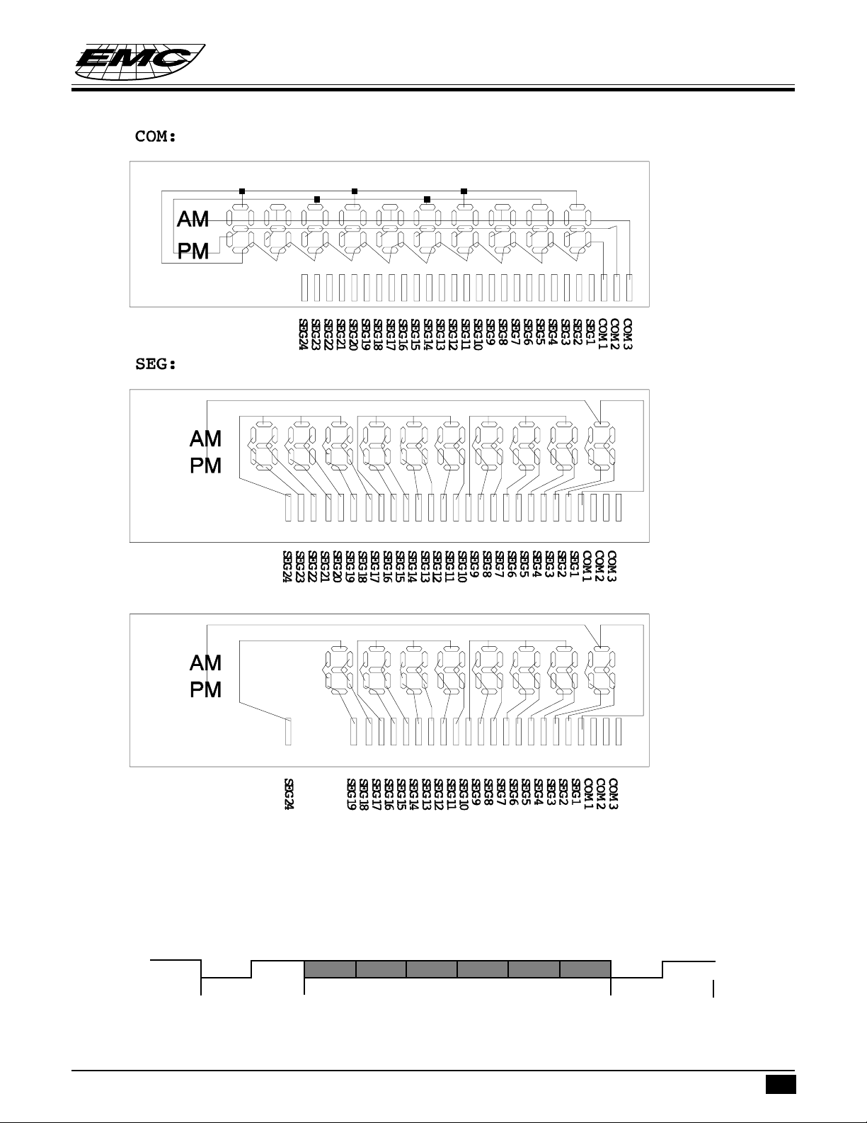
If SEG20~23 are not used, then it can be used as an 8 digits LCD display driver.
Serial Data Interface
When the EM32100 senses the falling edge of the Start bit, it will sample subsequent bits in the middle of
each bit. The received bit will then be assembled and decoded, and corresponding pattern will be displayed
on LCD panel. The serial data format is as follows:
0
Start bit
The frequence of every bit is 256Hz ( about 3.9 ms)
There are two categories of dialing data, and representation of serial data is as the following:
* This specification are subject to be changed without notice.
1
Bit0
Bit1
Bit2
Data bits
Bit3
Bit4 Bit5
0
Stop bit
1
2.10.1999
4
Page 5

8/10 DIGIT LCD DRIVER
F
F
T
F
F
T
F
T
F
T
F
F
T
T
T
F
F
F
T
T
T
T
F
F
T
T
T
T
F
D
ataValid?
27
RTC Mod
e
24
6Sec.Exp
ire
?
21
D
ataVali
d
?
20
D
ataIn?
19
6Sec.Exp
ire
?
18
HKS = 1?
17
S
tart Timer
16
DisplayDialing
No.
15
D
ataVali
d?
14
HKS=0
13
S
tartTimer
12
MS1 = 0?
11
D
ata i
n?
10
HKS = 1?
9
Display
RTC
8
MS1 = 0
7
MS2 = 0?
6
D
ataIn?
5
HKS = 1?
4
STW Display
3
R
eset S
TW
2
S
tart
1
T
F
MS2 = 0 ?
F
T
MS1=0?
MS2=0?
T
F
F
T
(b5b4 = 00) Digit key
Key 1234567890*#PP→T
b3b2b1b0 0001 0010 0011 0100 0101 0110 0111 1000 1001 1010 1011 1100 1101 1110
Display 1 2 34567890 P
(b5b4 = 10 ) function key
Key F
b3b2b1b0 1111
Display
Note:
1. Flash key will be treated as "clear LCD panel" command.
2. Any invalid data will be ignored by the EM32100.
FUNCTION DESCRIPTION
Dialing dispaly
EM32100
The serial data received by SDI pin of EM32100 will be decoded and shown on LCD panel. Display format
is as follows:
Off-Hook state mode:
* This specification are subject to be changed without notice.
2.10.1999
5
Page 6

RTC (Real time clock) display
12 hours format:
24 hours format:
EM32100
8/10 DIGIT LCD DRIVER
<Note>:
12 or 24 hours format is selected by 24/12 pin. When this pin is pulled "high", then RTC is displayed in 24
hours format, otherwise RTC is displayed in 12 hours format. The AM, PM patterns will not show for RTC
display in 24 hours format.
STW (stop watch ) display
When HKS pin is high, the system work in RTC display mode .When HKS pin switches from "high" to "low",
the system enter STW display mode.STW count up from 00:00 up to 59:59. For example:
* This specification are subject to be changed without notice.
2.10.1999
6
Page 7

EM32100
F
T
F
F T
F
F
F T
T
F
T
T
T
T
F
S
top Watch
M
ode
1
0
Minute +1
9
MS2 = L
o?
8
MS1 = L
o?
7
HKS=0?
6
Minute Flash and reset second
5
Hour +1
9
MS2 = L
o?
8
MS1 = L
o?
7
HKS=0 ?
6
Hour Flash
5
MS1 = L
o?
4
HKS=0 ?
3
RTC D
isplay
2
S
tart
1
8/10 DIGIT LCD DRIVER
Setting RTC
With the HKS pin at "high", RTC can be set up by operating MS1 and MS2 pins as described as in the following:
1.In on-Hook state, press MS1, hour digit will flash,
2. Press MS2 to count up data.
3.Press MS1 once again, move to minute digit, digit flash, and reset second.
4.Press MS2 to count up minute digit.
5.Press MS1 again to finish RTC set up.
<Note>:
1. If MS2 are pressed and hold for over 2 sec ,then data automatically count up in every 0.5 sec.
2. Digit flash time is 1 Hz (0.5 sec on, 0.5 sec off)
RTC setup Flowchart:
* This specification are subject to be changed without notice.
2.10.1999
7
Page 8

EM32100
8/10 DIGIT LCD DRIVER
RTC display and STW reset at Off-hook state
1.When at On-hook state,operating MS1 and MS2 can setup RTC.
2.When at Off-hook state,operating MS1 and MS2 can display RTC and clear STW.
Describe as following table:
HKS="high" HKS="low"
MS1 Select RTC setup position Toggle display RTC/STW
MS2 Count up hour or minute data Reset STW
Testing operating
The F32HZ pin is a 32 Hertz clock source. This pin is intended to support LCD module testing in production
line in the following two ways:
1. F32HZ can be connected to MS2 pin and, by operating the MS1 pin, can be used to test RTC setting
function.
2.At off-HOOK state; In the TEST mode (the TEST pin is at "Low" level), the SDI pin sampling signal frequency
is 32 Hz. F32HZ pin can be connected to SDI pin and with each reception of SDI data of "0" key, the LCD
will display "1", "2", ..., "9", *, #, P,P→T with each digit shifted left sequentially. Then the LCD panel goes
blank, AM,PM goes on, and finally all patterns go on. And this sequence will repeat again.
F32HZ
SDI
0
0
1
Bit 0
Start bit
• After entering test mode and 6 digits of "0" are received, the LCD panel is as follows:
•
Then 8 more digits of “0” are received, the LCD panel is as follows:
•
Then the LCD panel will go blank.
1
Bit 1
0
Bit 2
1
Bit 3
0
Bit 4
1
Bit 5
0
1
Stop bitData bits
* This specification are subject to be changed without notice.
2.10.1999
8
Page 9

•
Turn on “AM”indicator
AM
•
Then turn on “PM”indicator
PM
PM
•
Finally all patterns are turned on.
AM
EM32100
8/10 DIGIT LCD DRIVER
PM
• Then the sequence will repeat all over again.
ABSOLUTE MAXIMUM RATINGS
Items Sym. Condition Rating
Supply voltage V
Input voltage V
Output voltage V
DD
IN
O
Except open-drain - 0.5V to VEE+0.5V
- 0.5V to 1.5V
- 0.5V to VDD+0.5V
Open-drain -0.5 V to 3V
Output current I
Power dissipation P
Operating temperature T
Storage temperature T
O
D
OPR
STR
Others 3.2 mA
T
= 50oC 300 mW
OPR
0oC to 50oC
-55oC to 125oC
RECOMMENDED OPERATING CONDITIONS
1. Supply voltage at 1.5V D.C.
2. Operation frequency fosc : 32768 Hz.
* This specification are subject to be changed without notice.
2.10.1999
9
Page 10

EM32100
8/10 DIGIT LCD DRIVER
DC AND AC ELECTRICAL CHARACTERISTICS (fosc=32768 Hz,V
=1.5V)
DD
Parameter Sym. Condition Min. Typ. Max. Unit
Operating voltage V
V
Operating current (no load) I
DD
EE
DD
1.2 1.5 1.8 V
2.4 3 3.6 V
- 1.5 3 µA
Power on
crystal start oscillation voltage V
Input voltage V
V
Standby current (ENRTC=H) I
Input pins pull-up resistor R
START
IH
IL
STBY
I
1.3 1.5 1.8 V
VDD-0.3 - V
V
SS
-VSS+0.3 V
DD
--1µA
- 150 - KΩ
(MS1, TestI pins)
MS2 pin input resistance R
SDI pin input resistance R
SDI input data every bit time T
I
I
BIT
HKS=1, VI=V
HKS=0, V
VIN=V
I=VSS
SS
SS
-5-MΩ
- 150 - KΩ
-5-MΩ
3.8 3.9 4.1 mS
Oscillator frequency fosc. - 32768 - Hz
V
Oscillator start time T
START
VDD=1.45 - - 2 Sec.
Common/Segment pins
Source curent I
Sink current I
F32HZ pin sink current I
OH
OL
S
VO=VEE-0.5V 6 - - µA
VO=0.5 6 - - µA
VO=0.5V 0.2 0.5 - mA
HKS, MS1, TESTI, MS2 Tdb V
(not at test mode), input pin
debouce time
=0.5V - 15.6 - mS
O
* This specification are subject to be changed without notice.
2.10.1999
10
Page 11

APPLICATION CIRCUIT
8/10 Digits LCD Pannel
EM32100
8/10 DIGIT LCD DRIVER
.1µ
.1µ
CC
NC
ENRTC
24/12
V
SS
XOUT
NC
XIN
DD
V
HKS
SD1
MS2
MS1
V
12
11
10
9
8
7
6
5
4
3
2
1
2423222120191817161514
SEG17
SEG18
SEG19
SEG20
SEG21
SEG22
SEG23
SEG16
25
SEG15
26
SEG14
27
SEG13
28
SEG12
29
SEG11
30
SEG10
31
NC
32
SEG9
33
SEG8
34
SEG7
35
SEG6
36
EM32100
EE
V
SEG24
VN
VP
13
NC
1.5V
20p
32768Hz
20p
SEG5
SEG4
SEG3
SEG2
SEG1
COM1
COM2
COM3
TEST2
TEST1
3738394041424344454647
1
F32H
48
2
NC
100k
3
200k
DD
V
220k
HKS
SDO
220k
C945
3
1
2
1µ
47kDIODE
2
2
2
DIODE
1
2
C945
3
HDO
1
HFO
SS
V
100k
1
DIODE
* This specification are subject to be changed without notice.
2.10.1999
11
Page 12

PAD DIAGRAM
EM32100
8/10 DIGIT LCD DRIVER
VP
VN
V
SEG24
SEG23
SEG22
SEG21
SEG20
SEG19
SEG18
SEG17
XIN
6
SEG12
DD
V
5
(0,0)
31
SEG11
HKS
4
33 34
SEG10
SDI
3
SEG9
MS2
2
SEG8
MS1
1
35
SEG7
47
46
45
44
43
42
36
41
40
39
38
37
SEG6
F32H
TESTI
TEST2
COM3
COM2
COM1
SEG1
SEG2
SEG3
SEG4
SEG5
SS
XOUT
V
24/12
ENRTC
14
15
16
EE
17
18
19
20
21
22
23
24
26 27
25
SEG16
11
SEG15
10
SEG14
9
8
EM32100
28 29 30
SEG13
Chip Size : 2230 x 2480 µm
Pad No. Symbol X Y
1 MS1 712.8 992.2
2 MS2 561.6 992.2
3 SDI 412.2 992.2
4 HKS 261.0 992.2
5V
DD
103.5 1012.0
6 XIN -59.5 992.2
7
8 XOUT -209.8 1006.2
9V
SS
-371.8 1006.2
10 24/12 -523.9 992.2
11 ENRTC -673.3 992.2
12
13
14 VP -917.2 1033.6
15 VN -917.2 884.2
16 V
EE
-931.2 733.3
17 SEG24 -949.2 552.1
18 SEG23 -949.2 371.7
19 SEG22 -949.2 191.3
20 SEG21 -949.2 11.0
* This specification are subject to be changed without notice.
2.10.1999
12
Page 13

8/10 DIGIT LCD DRIVER
Pad No. Symbol X Y
21 SEG20 -949.2 -169.4
22 SEG19 -949.2 -349.7
23 SEG18 -949.2 -530.1
24 SEG17 -949.2 -710.5
25 SEG16 -895.7 -1074.2
26 SEG15 -715.3 -1074.2
27 SEG14 -535.0 -1074.2
28 SEG13 -354.6 -1074.2
29 SEG12 -174.2 -1074.2
30 SEG11 6.1 -1074.2
31 SEG10 186.5 -1074.2
32
33 SEG9 366.8 -1074.2
34 SEG8 547.2 -1074.2
35 SEG7 727.6 -1074.2
36 SEG6 907.9 -1074.2
37 SEG5 949.1 -723.1
38 SEG4 949.1 -542.7
39 SEG3 949.1 -362.3
40 SEG2 949.1 -182.0
41 SEG1 949.1 -1.6
42 COM1 917.1 237.0
43 COM2 917.1 388.2
44 COM3 917.1 539.4
45 TEST2 903.1 695.6
46 TESTI 903.1 845.0
47 F32H 903.1 996.2
48
EM32100
* This specification are subject to be changed without notice.
2.10.1999
13
 Loading...