

Datasheet ELM9709NBA, ELM9710NBA, ELM9711NBA, ELM9722CAA, ELM9724CAA Datasheet (ELM) [ru]
...Page 1
ELM97xxxxA ELM97xxxxA
ELM97xxxxA VOLTAGE DETECTOR
ELM97xxxxA ELM97xxxxA
■■
■ GENERAL DESCRIPTION
■■
ELM 97xxxxA Series is a CMOS voltage detector IC for battery-operated portable devices. It consists of a
very low-power-consumption reference voltage source, a comparator , an output driver, a hysteresis circuit,
and detection voltage setting resistors. Output logic is positive, therefore output level is low when VDD is
lower than detection voltage.
It can be used as a reset controller in microcomputer-based systems. And it can be widely applied to the
devices, such as battery checkers, switching circuit of back-up power source, power failure detectors, etc.
Two output styles are available, N-ch opendrain and CMOS output.
It is available in SOT-89 and SOT-23.
■■
■ FEATURES
■■
・ Low power operation : TYP. 1.0μ A (VDD = 1.5V)
・ Low voltage operation : Reset operation assured at 0.8V
・ High accuracy of detection voltage : ± 2.5%
・ Low temperature coefficient : TYP. -300ppm/℃ (Detection voltage <2.0V)
: TYP. -100ppm/℃ (Detection voltage ≧2.0V)
・ Very small package : SOT-89, SOT-23
■■
■ APPLICATION
■■
・ Reset for microcomputer
・ Battery checker
・ Power failure detector
・ Switching of back-up power source
■■
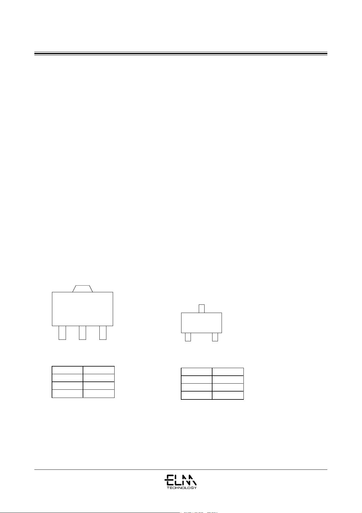
■ PIN CONFIGURATION
■■
SOT-89
1 23
( TOP VIEW )
Pin No. Pin Name
1 OUT
2 VDD
3 VSS
3
SOT-23
1 2
( TOP VIEW )
Pin No. Pin Name
1 OUT
2 VSS
3 VDD
147
Page 2
VOLTAGE DETECTOR ELM97xxxxA
■■
■ SELECTION GUIDE
■■
Symbol
Ex 09 : VDETN = 0.9V
a, b Detection Voltage
■■
■ SERIES
■■
c Output Form
d Package
e Product Version
C : CMOS Output
N : N-ch Opendrain Output
A : SOT-89
B : SOT-23
A : A Version
27 : VDETN = 2.7V
45 : VDETN = 4.5V
ELM97 x x x x AELM97 x x x x A
ELM97 x x x x A
ELM97 x x x x AELM97 x x x x A
↑↑↑↑↑↑↑↑↑↑
↑↑↑↑↑
↑↑↑↑↑↑↑↑↑↑
a b c d ea b c d e
a b c d e
a b c d ea b c d e
Model Package Model Package
ELM9709NBA-S(N) 0.9V N-ch SOT-23 ELM9727CAA-S(N) 2.7V CMOS SOT-89
ELM9710NBA-S(N) 1.0V N-ch SOT-23 ELM9730CAA-S(N) 3.0V CMOS SOT-89
ELM9711NBA-S(N) 1.1V N-ch SOT-23 ELM9732CAA-S(N) 3.2V CMOS SOT-89
ELM9722CAA-S(N) 2.2V CMOS SOT-89 ELM9734CAA-S(N) 3.4V CMOS SOT-89
ELM9724CAA-S(N) 2.4V CMOS SOT-89 ELM9745CAA-S(N) 4.5V CMOS SOT-89
ELM9725CAA-S(N) 2.5V CMOS SOT-89 ELM9748CAA-S(N) 4.8V CMOS SOT-89
S type : Standard, N type : Reverse
* Available 0.9V~5.0V detection voltage for N-ch output and 2.0V~5.0V detection voltage for CMOS
output at 0.1V step as semi-custom-made IC.
Detection Output Detection Output
Voltage Form Voltage Form
148
Page 3
VOLTAGE DETECTOR ELM97xxxxA
■■
■ MARKING
■■
SOT-89
①②
③④
Rule 1
① : Represents the integer digit of the detection voltage
Symbol Detection Voltage Symbol Detection Voltage
A 0.*V (N-ch) P 2.*V (CMOS)
B 1.*V (N-ch) R 3.*V (CMOS)
C 2.*V (N-ch) S 4.*V (CMOS)
D 3.*V (N-ch) T 5.*V (CMOS)
E 4.*V (N-ch)
F 5.*V (N-ch)
② : Represents the decimal digit of the detection voltage
SOT-23
①②③④
Symbol Detection Voltage Symbol Detection Voltage
0 *.0V 5 *.5V
1 *.1V 6 *.6V
2 *.2V 7 *.7V
3 *.3V 8 *.8V
4 *.4V 9 *.9V
③ : Represents the assembly lot number
A~ Z repeated (I,O,X excepted)
④ : Represents the assembly lot number
0~ 9 repeated
Rule 2
①: Represents the ELM97xxxxA series
ELM97xxxxA series = A
② : Represents the integer digit of the detection voltage
Symbol Detection Voltage Symbol Detection Voltage
0 0.*V (N-ch) Y 2.*V (CMOS)
1 1.*V (N-ch) W 3.*V (CMOS)
2 2.*V (N-ch) U 4.*V (CMOS)
3 3.*V (N-ch) V 5.*V (CMOS)
4 4.*V (N-ch)
5 5.*V (N-ch)
③ : Represents the decimal digit of the detection voltage
Symbol Detection Voltage Symbol Detection Voltage
0 *.0V 5 *.5V
1 *.1V 6 *.6V
2 *.2V 7 *.7V
3 *.3V 8 *.8V
4 *.4V 9 *.9V
④ : Represents the assembly lot number
0~ 9, A~ Z repeated (I,O,X excepted)
*Remarks --- ELM97xxxxA series have two kind of mraking rules each package.
149
Page 4
VOLTAGE DETECTOR ELM97xxxxA
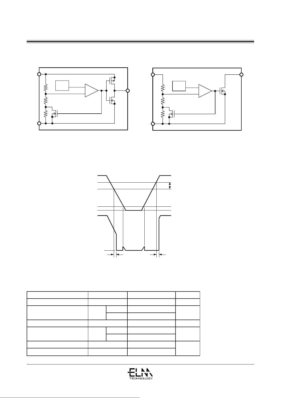
■■
■ BLOCK DIAGRAM
■■
1.CMOS Output 2.N-ch Opendrain Output
VDD
VREF
VSS
■■
■ TIMING CHART
■■
VDD
+
-
VDETP
VDETN
VopMin
VSS
OUT
VDD
VSS
VREF
VHYS
OUT
+
-
OUT
VSS
tPHL
■■
■ MAXIMUM ABSOLUTE RATINGS
■■
Parameter Limits Units
Power Supply Voltage 10 V
Output Voltage
Output Current 50 mA
Power Dissipation
Operating Temperature -30~+80
Storage Temperature -40~+125
Symbol
VOUT
Pd
VDD
CMOS VSS-0.3~VDD+0.3
N-ch VSS-0.3~+10
IOUT
SOT-89 300
SOT-23 200
Top
Tstg
tPLH
(VSS=0V)
V
mW
℃
150
Page 5

VOLTAGE DETECTOR ELM97xxxxA
■■
■ ELECTRICAL CHARACTERISTICS
■■
ELM9709NBA
ELM9709NBA
ELM9709NBAELM9709NBA
Param ete r Symbol Condition s Min. Typ. Max. Units Remarks
Detection Voltage
Hysteresis width
Current Consumption
Operating Voltage
Output Current
Delay Time
Temperature
Characteristics
of VDETN
ELM9710NBA
ELM9710NBA
ELM9710NBAELM9710NBA
Parameter Symbol Conditions Min. Typ. Max. Units Remarks
Detection Voltage
Hysteresis width
Current Consumption
Operating Voltage
Output Current
Delay Time
Temperature
Characteristic
of VDETN
(Top=25℃)
VDETN 0.878 0.900 0.922 V 2
VHYS
ISS VDD=1.5V - 1.0 3.0 μA1
VDD 0.8 - 6.0 V 2
IOUTN VDD=0.8V, VDS=0.5V 0.02 0.1 - mA 3
tPHL 2.0 mS 5
△VDETN
△Top
VDETN 0.975 1.000 1.025 V 2
VHYS
ISS VDD=1.5V - 1.0 3.0 μA1
VDD 0.8 - 6.0 V 2
IOUTN VDD=0.8V, VDS=0.5V 0.02 0.1 - mA 3
tPHL 2.0 mS 5
△VDETN
△Top
VDETN VDETN
×0.02 ×0.08
VDETN VDETN
×0.02 ×0.08
V
mV/℃
Remarks ) Test circuit No.
(Top=25℃)
V2-
-mV/℃ -Top=-30~+80℃ - -0.30
Remarks ) Test circuit No.
2
-Top=-30~+80℃ - -0.27 -
ELM9711NBA
ELM9711NBA
ELM9711NBAELM9711NBA
Param ete r Symbol Conditions Min. Typ. Max. Units Remarks
Detection Voltage
Hysteresis width
Current Consumption
Operating Voltage
Output Current
Delay Time
Temperature
Characteristic
of VDETN
(Top=25℃)
VDETN 1.073 1.100 1.127 V 2
VHYS
ISS VDD=1.5V - 1.0 3.0 μA1
VDD 0.8 - 6.0 V 2
IOUTN VDD=0.8V, VDS=0.5V 0.02 0.1 - mA 3
tPHL 2.0 mS 5
△VDETN
△Top
VDETN VDETN
×0.02 ×0.08
V2
mV/℃ -Top=-30~+80℃ --0.33-
Remarks ) Test circuit No.
151
Page 6

VOLTAGE DETECTOR ELM97xxxxA
ELM9722CAA
ELM9722CAA
ELM9722CAAELM9722CAA
Parameter Symbol Conditions Min. Typ. Max. Units Remarks
Detection Voltage
Hysteresis width
Current Consumption
Operating Voltage
Output Current
Delay Time
Temperature
Characteristic
of VDETN
ELM9724CAA
ELM9724CAA
ELM9724CAAELM9724CAA
Parameter Symbol Conditions Min. Typ. Max. Units Remarks
Detection Voltage
Hysteresis width
Current Consumption
Operating Voltage
Output Current
Delay Time
Temperature
Characteristic
of VDETN
(Top=25℃)
VDETN 2.145 2.200 2.255 V 2
VHYS
ISS VDD=3.0V - 1.5 4.5 μA1
VDD 0.8 - 6.0 V 2
IOUTN VDD=1.5V, VDS=0.5V 1.0 2.0 - mA 3
IOUTP VDD=4.5V, VDS=2.1V 0.5 1.5 - mA 4
tPHL 0.1 mS 5
△VDETN
△Top
VDETN 2.340 2.400 2.460 V 2
VHYS
ISS VDD=3.0V - 1.5 4.5 μA1
VDD 0.8 - 6.0 V 2
IOUTN VDD=1.5V, VDS=0.5V 1.0 2.0 - mA 3
IOUTP VDD=4.5V, VDS=2.1V 0.5 1.5 - mA 4
tPHL 0.1 mS 5
△VDETN
△Top
Top=-30~+80℃ --0.24
VDETN VDETN
×0.02 ×0.08
VDETN VDETN
×0.02 ×0.08
V2
mV/℃ -Top=-30~+80℃ - -0.22 -
Remarks ) Test circuit No.
(Top=25℃)
V2
-mV/℃ -
Remarks ) Test circuit No.
ELM9725CAA
ELM9725CAA
ELM9725CAAELM9725CAA
Parameter Symbol Conditions Min. Typ. Max. Units Remarks
Detection Voltage
Hysteresis width
Current Consumption
Operating Voltage
Output Current
Delay Time
Temperature
Characteristic
of VDETN
(Top=25℃)
VDETN 2.438 2.500 2.562 V 2
VHYS
ISS VDD=3.0V - 1.5 4.5 μA1
VDD 0.8 - 6.0 V 2
IOUTN VDD=1.5V, VDS=0.5V 1.0 2.0 - mA 3
IOUTP VDD=4.5V, VDS=2.1V 0.5 1.5 - mA 4
tPHL 0.1 mS 5
△VDETN
△Top
Top=-30~+80℃ -
VDETN - VDETN
×0.02 ×0.08
-0.25 -
Remarks ) Test circuit No.
V2
mV/℃ -
152
Page 7

VOLTAGE DETECTOR ELM97xxxxA
ELM9727CAA
ELM9727CAA
ELM9727CAAELM9727CAA
Parameter Symbol Conditions Min. Typ. Max. Units Remarks
Detection Voltage
Hysteresis width
Current Consumption
Operating Voltage
Output Current
Delay Time
Temperature
Characteristic
of VDETN
ELM9730CAA
ELM9730CAA
ELM9730CAAELM9730CAA
Parameter Symbol Conditions Min. Typ. Max. Units Remarks
Detection Voltage
Hysteresis width
Current Consumption
Operating Voltage
Output Current
Delay Time
Temperature
Characteristic
of VDETN
(Top=25℃)
VDETN 2.633 2.700 2.767 V 2
VHYS V
ISS VDD=4.5V - 1.5 4.5 μA1
VDD 0.8 - 6.0 V 2
IOUTN VDD=1.5V, VDS=0.5V 1.0 2.0 - mA 3
IOUTP VDD=4.5V, VDS=2.1V 0.5 1.5 - mA 4
tPHL 0.1 mS 5
△VDETN
△Top
VDETN 2.925 3.000 3.075 V 2
VHYS V
ISS VDD=4.5V - 1.5 4.5 μA1
VDD 0.8 - 6.0 V 2
IOUTN VDD=1.5V, VDS=0.5V 1.0 2.0 - mA 3
IOUTP VDD=4.5V, VDS=2.1V 0.5 1.5 - mA 4
tPHL 0.1 mS 5
△VDETN
△Top
Top=-30~+80℃ --0.27-mV/℃ -
Top=-30~+80℃ -0.30 - -mV/℃-
VDETN VDETN
×0.02 ×0.08
VDETN VDETN
×0.02 ×0.08
-
Remarks ) Test circuit No.
(Top=25℃)
-
Remarks ) Test circuit No.
2
2
ELM9732CAA
ELM9732CAA
ELM9732CAAELM9732CAA
Parameter Symbol Conditions Min. Typ. Max. Units Remarks
Detection Voltage
Hysteresis width
Current Consumption
Operating Voltage
Output Current
Delay Time
Temperature
Characteristic
of VDETN
(Top=25℃)
VDETN 3.120 3.200 3.280 V 2
VHYS
ISS VDD=4.5V - 1.5 4.5 μA1
VDD 0.8 - 6.0 V 2
IOUTN VDD=1.5V, VDS=0.5V 1.0 2.0 - mA 3
IOUTP VDD=4.5V, VDS=2.1V 0.5 1.5 - mA 4
tPHL 0.1 mS 5
△VDETN
△Top
Top=-30~+80℃ - -0.32 - mV/℃ -
VDETN VDETN
×0.02 ×0.08
V2
Remarks ) Test circuit No.
153
Page 8

VOLTAGE DETECTOR ELM97xxxxA
ELM9734CAA
ELM9734CAA
ELM9734CAAELM9734CAA
Parameter Symbol Conditions Min. Typ. Max. Units Remarks
Detection Voltage
Hysteresis width
Current Consumption
Operating Voltage
Output Current
Delay Time
Temperature
Characteristic
of VDETN
ELM9745CAA
ELM9745CAA
ELM9745CAAELM9745CAA
Parameter Symbol Conditions Min. Typ. Max. Units Remarks
Detection Voltage
Hysteresis width
Current Consumption
Operating Voltage
Output Current
Delay Time
Temperature
Characteristic
of VDETN
(Top=25℃)
VDETN 3.315 3.400 3.485 V 2
VHYS V
ISS VDD=4.5V - 1.5 4.5 μA1
VDD 0.8 - 6.0 V 2
IOUTN VDD=1.5V, VDS=0.5V 1.0 2.0 - mA 3
IOUTP VDD=4.5V, VDS=2.1V 0.5 1.5 - mA 4
tPHL 0.1 mS 5
△VDETN
△Top
VDETN 4.388 4.500 4.612 V 2
VHYS
ISS VDD=6.0V - 1.5 4.5 μA1
VDD 0.8 - 6.0 V 2
IOUTN VDD=1.5V, VDS=0.5V 1.0 2.0 - mA 3
IOUTP VDD=6.0V, VDS=2.1V 0.5 2.0 - mA 4
tPHL 0.1 mS 5
△VDETN
△Top
Top=-30~+80℃ -
Top=-30~+80℃ --0.45- -mV/℃
VDETN VDETN
×0.02 ×0.08
VDETN VDETN
×0.02 ×0.08
-
-0.34 mV/℃
-
-
Remarks ) Test circuit No.
V2
Remarks ) Test circuit No.
(Top=25℃)
2
-
ELM9748CAA
ELM9748CAA
ELM9748CAAELM9748CAA
Param ete r Symbol Conditions Min. Typ. Max. Units Remarks
Detection Voltage
Hysteresis width
Current Consumption
Operating Voltage
Output Current
Delay Time
Temperature
Characteristic
of VDETN
(Top=25℃)
VDETN 4.680 4.800 4.920 V 2
VHYS V
ISS VDD=6.0V - 1.5 4.5 μA1
VDD 0.8 - 6.0 V 2
IOUTN VDD=1.5V, VDS=0.5V 1.0 2.0 - mA 3
IOUTP VDD=6.0V, VDS=2.1V 0.5 2.0 - mA 4
tPHL 0.1 mS 5
△VDETN
△Top
Top=-30~+80℃ --
VDETN VDETN
×0.02 ×0.08
-
-0.48 - mV/℃
Remarks ) Test circuit No.
154
2
Page 9

VOLTAGE DETECTOR ELM97xxxxA
■■
■ TYPICAL CHARACTERISTICS
■■
● ELM9711NxA
ISS - VDD
4
3
80
℃
25
2
℃
ISS (μA)
1
-30
℃
0
1 2 3
4
3
2
VOUT (V)
25
1
80℃
0
VDD (V)
IOUT - VDS
1
0.8
0.6
0.4
IOUT (mA)
0.2
VDD=1.0V
VDD=0.8V
2
1.5
1
IOUT (mA)
0.5
VOUT - VDD
-30℃
℃
1 2 3
VDD (V)
IOUT - VDD
25℃
(3V Pullup 1MΩ)
℃
80
-30℃
0.2 0.4 0.6 0.8
0
1.2
VDET (V)
1.1
VDETN
-20 0 20 40 60 80
VDS (V)
VDET - Top
Top ( ℃)
VDETP
0
0.6 0.8 1 1.2 1.4
VDD (V)
tPHL,tPLH - VDD
100
10
tPHL,tPLH (ms)
1
0.1
0.001 0.01 0.1 1
tPLH
tPHL
CL (μF)
155
Page 10

VOLTAGE DETECTOR ELM97xxxxA
■■
■ TEST CIRCUITS
■■
1. Current Consumption 2. Detection Voltage
A
VDD
VDD
ELM97
OUT
Series
VSS
3. Output Current (N-ch) 4. Output Current (P-ch)
VDD
V
* R=1M Ω
VDD
ELM97
Series
VSS
OUT
R*
3V
VDETN
VDD
VDD VDD
V
ELM97
Series Series
VSS VSS
OUT
A
VDS VDS
VDD
V
V
5. Delay Time Input Pulse
R*
●
3V
CL
→
P.G.
VDD
ELM97
Series
VSS
OUT
●●
ELM97
V
OUT
A
3 or 6V
0.8V
* R=1M Ω
R is unnecessary for CMOS output products.
156
VSS
Page 11

 Loading...