

Page 1
ELM380
1234876
5
Battery Charger Timer
Description
4
5
2
7
3
6
Features
The ELM380 is an 8 pin integrated circuit that is
used to provide very long time interval outputs. It is
typically used for enabling the charge circuit in
Nickel Cadmium battery chargers, but can be easily
adapted for many other applications.
An express ‘one button’ mode is provided on
chip specifically for rechargeable battery circuits. In
this mode, pressing the start button once initiates a
user selectable 8 or 14 hour timing interval, after
which the circuit shuts off. If one prefers, pressing
that same button multiple times will allow for user
programmable intervals of from 2 to 77 hours.
The circuit requires a 60Hz full-wave rectified
signal for its operation. This 120Hz time base is
used for all of the timekeeping functions, providing
good long term stability and low cost.
Interfacing to the ELM380 is simplified by the
provision of internal pull-up resistors so that the
mechanical switches can be directly connected
without additional components, or simply not used,
depending on the application.
Applications
• Low power CMOS design - typically 1mA at 5V
• Wide supply range - 3.0 to 5.5 volt operation
• Quick settings of 8 or 14 hours
• Complementary outputs simplify designs
• External reset input for system use
• Internal pullup resistors for switch inputs
• High current drive outputs - up to 25 mA
• Line frequency input for accurate timing
Connection Diagram
PDIP and SOIC
(top view)
VDD VSS
Out
Out
reset
start
8/14 hrs
Clock
• Ni-Cd battery chargers
• Yard lighting or watering controls
• Houseplant grow lamp controllers
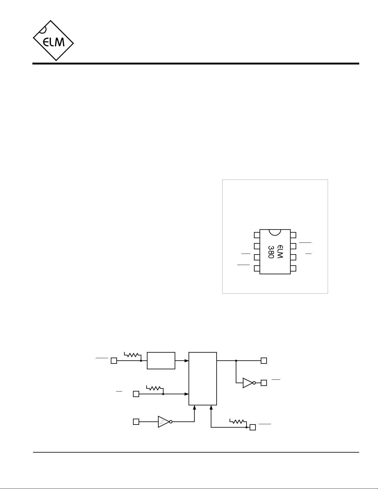
Block Diagram
start
8/14 hrs
Clock
ELM380DSB
VDD
Debounce
Timers
Control
VDD
and
Counters
VDD
Elm Electronics – Circuits for the Hobbyist
< http://www.elmelectronics.com/ >
Out
Out
reset
1 of 4
Page 2

ELM380
Pin Descriptions
VDD (pin 1)
This pin is the positive supply pin, and should
always be the most positive point in the circuit.
Internal circuitry connected to this pin is used to
provide power on reset of the microprocessor, so
an external reset signal is normally not required.
Refer to the Electrical Characteristics section for
further information.
Out (pin 2), and Out (pin 3)
These are the two complementary timer outputs.
During a timing interval, pin 2 will go to a high
logic level, and pin 3 will go low.
reset (pin 4)
This is an active low master reset input. If unused,
it can be left open circuited (due to the internal
resistor), or tied to VDD.
Clock (pin 5)
This is the master timekeeping input. Normally a
60Hz full-wave, positive going signal is applied to
this Schmitt trigger input. Due to the internal
clamp diodes, often the only other component
required is a series connected resistor. Some
circuit configurations may require a pulldown
resistor to prevent the possibility of having a
floating input.
8/14 hrs (pin 6)
This input pin selects either an eight hour (if
high) or a 14 hour (if low) time interval when in
the quick programming mode. The state of this
pin is only determined at the end of eight hours.
start (pin 7)
A single momentary low on this pin is used to
initiate a quick programming cycle of either 8 or
14 hours. Pressing this switch multiple times will
program the timer for operation with the number
of hours equal to the number of button presses.
When there is more than two seconds with no
switch activity, the circuit will assume that
programming is complete, and issue a short
(0.5sec) ‘output off’ to signal the user.
This input also provides an abort function which
cancels any timing cycle that is in progress, if the
input is held continuously low for more than
three seconds. An internal debouncing circuit
and a pullup resistor are provided on this pin to
assist with the interface to mechanical switches.
VSS (pin 8)
Circuit common is connected to this pin. This is
the most negative point in the circuit.
Ordering Information
All rights reserved. Copyright ©1999 Elm Electronics.
Every effort is made to verify the accuracy of information provided in this document, but no representation or warranty can be
given and no liability assumed by Elm Electronics with respect to the accuracy and/or use of any products or information
described in this document. Elm Electronics will not be responsible for any patent infringements arising from the use of these
products or information, and does not authorize or warrant the use of any Elm Electronics product in life support devices and/or
systems. Elm Electronics reserves the right to make changes to the device(s) described in this document in order to improve
reliability, function, or design.
ELM380DSB
These integrated circuits are available in either the 300 mil plastic DIP format, or in the 200 mil SOIC surface
mount type of package. To order, add the appropriate suffix to the part number:
300 mil Plastic DIP............................... ELM380P 200 mil SOIC.....................................ELM380SM
Elm Electronics – Circuits for the Hobbyist
< http://www.elmelectronics.com/ >
2 of 4
Page 3

ELM380
Absolute Maximum Ratings
Stresses beyond those listed here will likely damage
the device. These values are given as a design
guideline only. The ability to operate to these levels
is neither inferred nor recommended.
Storage Temperature.......................-65°C to +150°C
Note:
Ambient Temperature with
Power Applied....................................-40°C to +85°C
Voltage on VDD with respect to VSS............0 to +7.5V
Voltage on any other pin with
respect to VSS........................... -0.6V to (VDD + 0.6V)
Electrical Characteristics
All values are for operation at 25°C and a 5V supply, unless otherwise noted. For further information, refer to note 1 below.
Characteristic Minimum Typical Maximum ConditionsUnits
Supply Voltage, VDD 3.0 5.0 5.5 V
VDD rate of rise 0.05 V/ms
Average Supply Current, IDD 1.0 2.4 mA
Internal pullup resistances 300 500 600 KΩ Pin 4 (reset)
(see note 4)
20 30 50 KΩ Pin 6 (8/14) & pin 7 (start)
see note 2
VDD = 5V, see note 3
Debounce period - start input msec50
Input current -0.5 +0.5 mA
Input low voltage VSS 0.15 VDD V
Input high voltage VDD V0.85 VDD
Output low voltage 0.6 V
Output high voltage VVDD - 0.7
Notes:
1. This integrated circuit is produced with a Microchip Technology Inc.’s PIC12C5XX as the core embedded
microcontroller. For further device specifications, and possibly clarification of those given, please refer to the
appropriate Microchip documentation.
2. This spec must be met in order to ensure that a correct power on reset occurs. It is quite easily achieved
using most common types of supplies, but may be violated if one uses a slowly varying supply voltage, as
may be obtained through direct connection to solar cells, or some charge pump circuits.
3. Pullup resistor currents are not included in this figure.
4. The value of the internal pullup resistance is both supply and temperature dependent.
5. This specification represents current flowing through the protection diodes when applying large voltages to
the clock input (pin 5) through a current limiting resistance. Currents quoted are the maximum continuous.
with 120Hz (60Hz full-wave) clock
clock input only, see note 5
Current (sink) = 8.7mA
Current (source) = 5.4mA
ELM380DSB
Elm Electronics – Circuits for the Hobbyist
3 of 4
< http://www.elmelectronics.com/ >
Page 4

Example Application
ELM380
1234876
5
Figure 1 shows the ELM380 used in a typical
battery charger control circuit.
Power for this circuit is obtained from a 12V supply,
as shown. Usually there will be a voltage of about this
level available if the charger is to support 9V batteries.
The 12V has been reduced to 5V through a 78L05 low
power regulator. This is a relatively inexpensive and
convenient way to obtain a stable voltage for a circuit
such as this.
The required 120Hz for the clock input is obtained
from the full-wave bridge as shown below. A series
diode has been added to prevent back-feed from the
filter capacitors (which would put a constant high level
on the clock input), and a 47KΩ resistor is connected in
series with pin 5 to limit the current through the
protection diodes when the AC bridge voltage exceeds
the ELM380 supply levels.
After the peak of each sine wave, the series diode,
and for a time, the bridge diodes, will not be conducting.
This means that the clock input will be left floating,
which is not advisable with CMOS circuits. To provide a
+12V
12V Relay
Charger
Enable
1N4001
+5V
ground reference during these ‘open circuit’ periods, the
100KΩ resistor was connected from this point to VSS.
The rest of the circuit is straightforward. Two
switches are provided for control. Both the momentary
action ‘start’ switch and the toggle type ‘8/14’ switch
have 300Ω series resistors for added ESD protection,
and rely on the internal pullup resistors to provide a full
logic swing when operated. The 300Ω resistors aren’t
strictly required, but are a nice addition to consider for
added protection.
Only one of the outputs is used for this circuit. Its
active high level is used to drive the NPN transistor into
conduction and energize the relay coil. Depending on
the circuit, a direct connection to the load might be
used, but the use of a relay allows for general control of
many different loads.
There are many other uses that this circuit could be
put to. It could actually be used for almost any
application that needs long time intervals… Lawn
watering controls… Auto-off lighting systems…
300Ω
start
2.2KΩ
2N3904
47KΩ
100KΩ
+12V
10VAC
60Hz
Supply
150µF
+
0.1µF
Figure 1. Typical Charger Control Circuit
ELM380DSB Elm Electronics – Circuits for the Hobbyist
< http://www.elmelectronics.com/ >
300Ω
8/14
open for 8 hrs
closed for 14
+5V
78L05
0.1µF
4 of 4
 Loading...