

Page 1

Description
The CXP922P032 is a CMOS 16-bit microcomputer
integrating on a single chip an A/D converter, serial
interface, timer, remote control receive circuit, PWM
output circuit, and as well as basic configurations like a
16-bit CPU, PROM, RAM, and I/O port.
This LSI also provides the sleep/stop functions that
enable lower power consumption.
The CXP922P032 is the PROM-incorporated
version of the CXP922032 with built-in mask ROM.
This provides the additional feature of being able to
write directly into the program. Thus, it is most
suitable for evaluation use during system
development and for small-quantity production.
Features
• An efficient instruction set as a controller
— Direct addressing, numerous abbreviated forms, multiplication and division instructions
• Instruction sets for C language and RTOS
— Highly quadratic instruction system, general-purpose register of eight 16-bit × 16-bank configuration
• Minimum instruction cycle 100ns/20MHz operation (3.0 to 5.5V)
167ns/12MHz operation (2.7 to 5.5V)
• Incorporated PROM capacity 128K bytes
• Incorporated RAM capacity 7680 bytes
• Peripheral functions
— A/D converter
8-bit 8 analog input, successive approximation system
(Conversion time:
12.4µs at 20MHz)
— Serial interface Asynchronous serial interface (Simple UART)
128-byte buffer RAM,3 channels
— Timers 8-bit timer/counter, 2 channels (with timing output)
16-bit capture timer/counter (with timing output)
16-bit timer, 4 channels
— Remote control receive circuit 8-bit pulse measurement counter, 8-stage FIFO
— PWM output circuit 14-bit, 1 channel
• Interruption 24 factors, 24 vectors, multi-interruption and priority selection possible
• Standby mode Sleep/stop
• Package 100-pin plastic QFP
• Piggy/evaluation chip CXP922000
•
Mask ROM
CXP922032
Structure
Silicon gate CMOS IC
– 1 –
E99937-PS
Sony reserves the right to change products and specifications without prior notice. This information does not convey any license by
any implication or otherwise under any patents or other right. Application circuits shown, if any, are typical examples illustrating the
operation of the devices. Sony cannot assume responsibility for any problems arising out of the use of these circuits.
CXP922P032
CMOS 16-bit Single Chip Microcomputer
100 pin QFP (Plastic)
For the availability of this product, please contact the sales office.
Page 2
– 2 –
CXP922P032
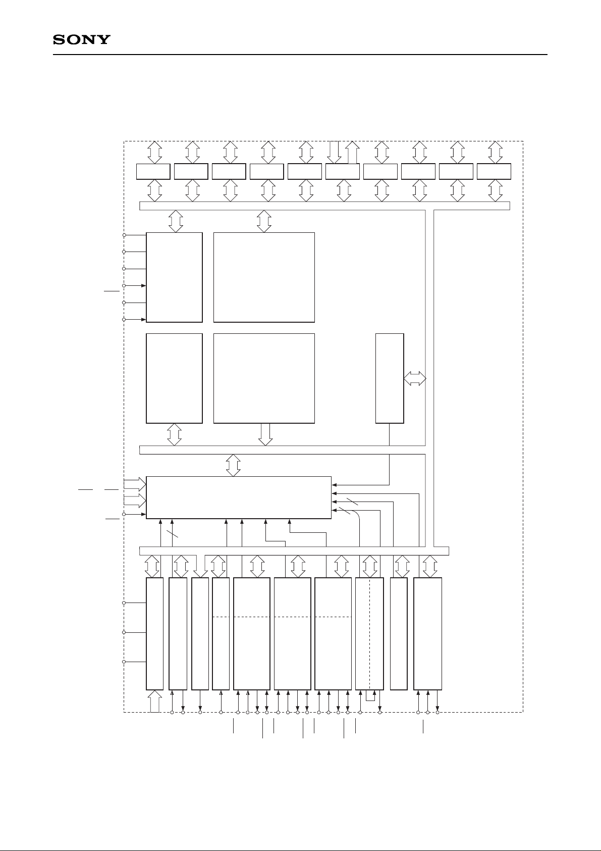
Block Diagram
A/D CONVERTER
8
5 7
AN0 to AN7 PA0 to PA7
AVREF
AVSS
AVDD
NMI
INT0 to INT4
PB0 to PB7
PC0 to PC7
PD0 to PD7
PE0 to PE7
PF0 to PF5
PF6, PF7
PG0 to PG7
PH0 to PH7
PI0 to PI7
PJ0 to PJ6
RxD
TxD
PWM
RMC
CS0
SO0
SI0
SCK0
SI1
CS1
SCK1
SO1
CS2
SO2
SI2
SCK2
TO0
EC0
EC1
CINT
TO1
SPC950
CPU CORE
CLOCK GENERATOR/
SYSTEM CONTROLLER
PORT A
UART
14-BIT PWM GENERATOR
REMOCON
4CH 16-BIT TIMER
FIFO
SERIAL
INTERFACE
UNIT (CH0)
BUFFER
RAM
SERIAL
INTERFACE
UNIT (CH1)
BUFFER
RAM
SERIAL
INTERFACE
UNIT (CH2)
BUFFER
RAM
8-BIT TIMER/COUNTER (CH0)
8-BIT TIMER (CH1)
16-BIT CAPTURE
TIMER/COUNTER (CH4)
PRESCALER/
TIME-BASE TIMER
2
PROM
128K BYTES
8
PORT B
8
PORT C
8
PORT D
INTERRUPT CONTROLLER
8
PORT E
8
PORT F
6
2
PORT G
8
PORT H
8
PORT I
8
PORT J
7
RAM
7680 BYTES
KS0 to KS6
2
4
VDD
RST
XTAL
EXTAL
VSS
VPP
Page 3
– 3 –
CXP922P032
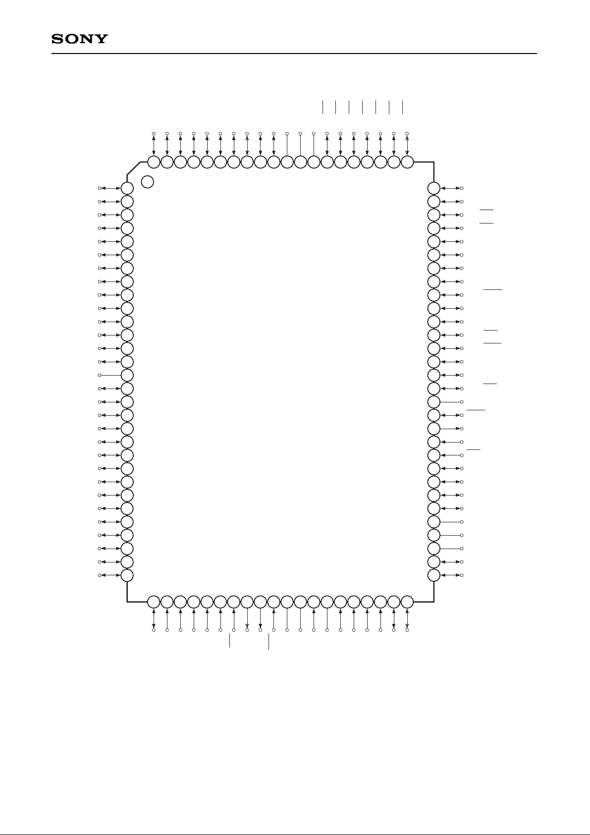
Pin Assignment (Top View) 100-pin QFP package
31 32 33 34 35 36 37 38 39 40 41 42 43 44 454647 48 49 50
57
58
59
60
61
62
63
64
65
66
67
68
69
70
71
72
73
74
75
76
77
78
79
80
81828384858687888990919293949596979899
1
2
3
4
5
6
7
8
9
10
11
12
13
14
15
16
17
18
19
20
21
22
23
24
PE7
PF0/INT0
PF1/INT1
PF2/INT2
PF3/INT3
PF4/INT4
PF5/NMI
PF6/TO0
PF7/TO1/PWM
RST
V
SS
XTAL
EXTAL
V
DD
AN0
AN1
AN2
AN3
PG0/AN4
PG1/AN5
PI7/RMC
PI6/CINT
PI5/EC1
PI4/EC0
PI3
PI2
PI1/RxD
PI0/TxD
PH7/SCK2
PH6/SO2
PH5/SI2
PH4/CS2
PH3/SCK1
PH2/SO1
PH1/SI1
PH0/CS1
V
SS
SCK0
SO0
SI0
CS0
PG7
PG6
PG5
PG4
51
52
53
54
55
56
AV
DD
AVREF
AVSS
PG3/AN7
PG2/AN6
PB2
PB3
PB4
PB5
PB6
PB7
PC0
PC1
PC2
PC3
PC4
PC5
PC6
PC7
V
SS
PD0
PD1
PD2
PD3
PD4
PD5
PD6
PD7
PE0
25
26
27
28
29
PE1
PE2
PE3
PE4
PE5
30
PE6
PB1
PB0
PA7
PA6
PA5
PA4
PA3
PA2
PA1
PA0
VSSVDD
VPP
PJ6/KS6
PJ5/KS5
PJ4/KS4
PJ3/KS3
PJ2/KS2
PJ1/KS1
PJ0/KS0
100
Notes) 1. Do not make any connections to VPP (Pin 88).
2. VSS (Pins 15, 41, 64 and 90) must be connected to GND.
3. VDD (Pins 44 and 89) must be connected to VDD.
– 4 –
Page 4
CXP922P032
Pin Functions
Symbol I/O
Functions
PA0 to PA7
I/O
(Port A)
8-bit I/O port.
I/O can be specified in 1-bit units.
Pull-up resistor is present or not through program in 4-bit units.
(8 pins)
PB0 to PB7 I/O
(Port B)
8-bit I/O port.
I/O can be specified in 1-bit units.
Pull-up resistor is present or not through program in 4-bit units.
(8 pins)
PC0 to PC7 I/O
(Port C)
8-bit I/O port.
I/O can be specified in 1-bit units.
Pull-up resistor is present or not through program in 4-bit units.
(8 pins)
PD0 to PD7
I/O
(Port D)
8-bit I/O port.
I/O can be specified in 1-bit units.
Pull-up resistor is present or not through program in 4-bit units.
Can drive 12mA sink current (VDD = 4.5 to 5.5V).
(8 pins)
PE0 to PE7
I/O
(Port E)
8-bit I/O port.
I/O can be specified in 1-bit units.
Pull-up resistor is present or not through program in 4-bit units.
Can drive 12mA sink current (VDD = 4.5 to 5.5V).
(8 pins)
(Port F)
8-bit port.
Lower 6 bits are for input;
upper 2 bits are for output.
(6 pins)
PF0/INT0
to PF4/INT4
Input / Input
External interrupt inputs.
(4 pins)
PF5/NMI
Input / Input
Non-maskable interrupt input.
PF6/TO0
Output / Output
8-bit timer/counter output.
PF7/TO1/
PWM
Output / Output /
Output
16-bit capture timer/
counter output.
AN0 to AN3
Input
Analog input for A/D converter.
(4 pins)
Analog input for A/D
converter.
(4 pins)
PG0/AN4
to PG3/AN7
I/O / Input
PG4 to PG7
I/O
(Port G)
8-bit I/O port.
I/O can be specified in 1-bit units.
Pull-up resistor is present or not through
program in 4-bit units.
(8 pins)
14-bit PWM output.
CS0
SI0
SO0
SCK0
Input
Input
Output
I/O
Serial chip select (CH0) input.
Serial data (CH0) input.
Serial data (CH0) output.
Serial clock (CH0) I/O.
Page 5
– 5 –
CXP922P032
Symbol I/O
Functions
PH0/CS1
PH1/SI1
PH2/SO1
PH3/SCK1
PH4/CS2
PH5/SI2
PH6/SO2
PH7/SCK2
PI0/TxD
PI1/RxD
PI2 to PI3
PI4/EC0
PI5/EC1
PI6/CINT
PI7/RMC
PJ0/KS0
to PJ6/KS6
I/O / Input
I/O / Input
I/O / Output
I/O / I/O
I/O / Input
I/O / Input
I/O / Output
I/O / I/O
I/O / Output
I/O / Input
I/O
I/O / Input
I/O / Input
I/O / Input
I/O / Input
I/O / Input
(Port H)
8-bit I/O port.
I/O can be specified in
1-bit units.
Pull-up resistor is present
or not through
program in 4-bit units.
(8 pins)
(Port I)
8-bit I/O port.
I/O can be specified in
1-bit units.
Pull-up resistor is present
or not through
program in 4-bit units.
(8 pins)
(Port J)
7-bit I/O port.
I/O can be specified in
1-bit units.
Pull-up resistor is present
or not through
program in lower 4-bit
units and upper 3-bit units.
(7 pins)
Serial chip select (CH1) input.
Serial data (CH1) input.
Serial data (CH1) output.
Serial clock (CH1) I/O.
Serial chip select (CH2) input.
Serial data (CH2) input.
Serial data (CH2) output.
Serial clock (CH2) I/O.
UART transmission data output.
UART reception data input.
External event input for 8-bit timer/counter.
External event input for 16-bit capture timer/
counter.
External capture input for 16-bit capture timer/
counter.
Remote control receive circuit input.
Standby release input function can be specified
in 1-bit units.
(7 pins)
EXTAL
XTAL
RST
AVDD
AVREF
AVSS
VDD
VSS
VPP
Input
Input
Input
Connects a crystal for system clock oscillation.
(When the clock is supplied externally, input it to EXTAL and input an
opposite phase clock to XTAL.)
System reset. Active at "L" level.
Positive power supply for A/D converter.
Reference voltage input for A/D converter.
GND for A/D converter.
Positive power supply.
(Connect both VDD pins to positive power supply.)
GND
(Connect all four VSS pins to GND.)
Positive power supply pin used for writing inorporated PROM.
(Do not make any cunnection to NC.)
Page 6
– 6 –
CXP922P032
I/O Circuit Format for Pins
Pin Circuit format
After a reset
PA0 to PA7
Hi-Z
PUL0 register
"0" after a reset
Internal data bus
Input protection
circuit
IP
∗
∗
Pull-up transistor
approximately 100kΩ (V
DD = 4.5 to 5.5V)
approximately 150kΩ (V
DD = 3.0 to 3.6V)
RD
PA register
Undefined after a reset
PAD register
"0" after a reset
PB0 to PB7 Hi-Z
PUL0 register
"0" after a reset
Internal data bus
IP
∗
∗
Pull-up transistor
approximately 100kΩ (V
DD = 4.5 to 5.5V)
approximately 150kΩ (V
DD = 3.0 to 3.6V)
RD
PB register
Undefined after a reset
PBD register
"0" after a reset
PC0 to PC7 Hi-Z
PUL0 register
"0" after a reset
Internal data bus
IP
∗
∗
Pull-up transistor
approximately 100kΩ (V
DD = 4.5 to 5.5V)
approximately 150kΩ (V
DD = 3.0 to 3.6V)
RD
PC register
Undefined after a reset
PCD register
"0" after a reset
Page 7
– 7 –
CXP922P032
Pin
Circuit format After a reset
PD0 to PD7
Hi-Z
PF0/INT0
to PF4/INT4
PF5/NMI
Hi-Z
PUL0 register
"0" after a reset
Internal data bus
IP
∗
1
Pull-up transistor
approximately 100kΩ (V
DD = 4.5 to 5.5V)
approximately 150kΩ (V
DD = 3.0 to 3.6V)
∗
2
Large current drive
12mA (V
DD = 4.5 to 5.5V)
4.5mA (V
DD = 3.0 to 3.6V)
RD
∗1
∗2
PD register
Undefined after a reset
PDD register
"0" after a reset
PE0 to PE7
Hi-Z
PUL1 register
"0" after a reset
Internal data bus
IP
∗
1
Pull-up transistor
approximately 100kΩ (V
DD = 4.5 to 5.5V)
approximately 150kΩ (V
DD = 3.0 to 3.6V)
∗
2
Large current drive
12mA (V
DD = 4.5 to 5.5V)
4.5mA (V
DD = 3.0 to 3.6V)
RD
∗1
∗2
PE register
Undefined after a reset
PED register
"0" after a reset
Internal data bus
CMOS Schmitt input
RD
INT0, INT1, INT2,
INT3, INT4, NMI
IP
Page 8
– 8 –
CXP922P032
Pin
Circuit format After a reset
PF6/TO0
"H" level
PF7/TO1/
PWM
"H" level
("H" level at ON
resistance of
pull-up transistor
during a reset.)
TO0
RD
Internal data bus
PFSL register
"0" after a reset
PF register
"1" after a reset
PFSL register (Bit 7)
PFSL register (Bit 6)
TO1 output enable
TO1
PWM
∗
Pull-up transistor
approximately 150kΩ (V
DD = 4.5 to 5.5V)
approximately 200kΩ (V
DD = 3.0 to 3.6V)
RD
Internal data bus Internal reset signal
∗
01
MPX
1x
00
PF register
"1" after a reset
"00" after a reset
Hi-Z
AN0 to AN3
IP
A/D converter
Input multiplexer
Page 9

– 9 –
CXP922P032
Pin Circuit format
After a reset
PG0/AN4
to PG3/AN7
Hi-Z
∗
∗
Pull-up transistor
approximately 100kΩ (V
DD = 4.5 to 5.5V)
approximately 150kΩ (V
DD = 3.0 to 3.6V)
Internal data bus
IP
RD
A/D converter
Input multiplexer
PUL1 register
"0" after a reset
PG register
Undefined after a reset
PGSL register
"0" after a reset
PGD register
"0" after a reset
PG4 to PG7 Hi-Z
PUL1 register
"0" after a reset
Internal data bus
IP
∗
∗
Pull-up transistor
approximately 100kΩ (V
DD = 4.5 to 5.5V)
approximately 150kΩ (V
DD = 3.0 to 3.6V)
RD
PG register
Undefined after a reset
PGD register
"0" after a reset
Page 10

– 10 –
CXP922P032
PH0/CS1
PH1/SI1
PH4/CS2
PH5/SI2
Hi-Z
∗
Pull-up transistor
approximately 100kΩ (V
DD = 4.5 to 5.5V)
approximately 150kΩ (V
DD = 3.0 to 3.6V)
Internal data bus
IP
RD
CMOS Schmitt input
∗
CS1, SI1, CS2, SI2
PUL1 register
"0" after a reset
PH register
Undefined after a reset
PHD register
"0" after a reset
SCK0
SCK0
SCK0 output enable
SCK0
IP
CMOS Schmitt input
"H" level
(Hi-Z during a
reset)
Pin
Circuit format After a reset
CS0
SI0
Hi-Z
Hi-Z
SO0
CMOS Schmitt input
IP
CS0
SI0
SO0
SO0 output enable
Page 11

– 11 –
CXP922P032
PI0/TxD Hi-Z
∗
Pull-up transistor
approximately 100kΩ (V
DD = 4.5 to 5.5V)
approximately 150kΩ (V
DD = 3.0 to 3.6V)
TxD output enable
Internal data bus
IP
∗
RD
TxD
PUL2 register
"0" after a reset
PI register
Undefined after a reset
PID register
"0" after a reset
Pin Circuit format After a reset
PH2/SO1
PH6/SO2
Hi-Z
∗
Pull-up transistor
approximately 100kΩ (V
DD = 4.5 to 5.5V)
approximately 150kΩ (V
DD = 3.0 to 3.6V)
SO1, SO2 output enable
Internal data bus
IP
RD
SO1, SO2
∗
PUL1 register
"0" after a reset
PHSL register
"0" after a reset
PHD register
"0" after a reset
PH register
Undefined after a reset
PH3/SCK1
PH7/SCK2
Hi-Z
SCK1, SCK2
CMOS Schmitt input
∗
Pull-up transistor
approximately 100kΩ (V
DD = 4.5 to 5.5V)
approximately 150kΩ (V
DD = 3.0 to 3.6V)
SCK1, SCK2 output enable
Internal data bus
IP
RD
SCK1, SCK2
∗
PUL1 register
"0" after a reset
PHSL register
"0" after a reset
PHD register
"0" after a reset
PH register
Undefined after a reset
Page 12

– 12 –
CXP922P032
Pin Circuit format After a reset
PI1/RxD
PI4/EC0
PI5/EC1
PI6/CINT
PI7/RMC
Hi-Z
∗
Pull-up transistor
approximately 100kΩ (V
DD = 4.5 to 5.5V)
approximately 150kΩ (V
DD = 3.0 to 3.6V)
Internal data bus
IP
RD
CMOS Schmitt input
∗
PUL2 register
"0" after a reset
PI register
Undefined after a reset
PID register
"0" after a reset
RxD, EC0, EC1, CINT, RMC
PI2 to PI3
Hi-Z
PUL2 register
"0" after a reset
Internal data bus
IP
∗
∗
Pull-up transistor
approximately 100kΩ (V
DD = 4.5 to 5.5V)
approximately 150kΩ (V
DD = 3.0 to 3.6V)
RD
PI register
Undefined after a reset
PID register
"0" after a reset
PJ0/KS0
to PJ6/KS6
Hi-Z
∗
Pull-up transistor
approximately 100kΩ (V
DD = 4.5 to 5.5V)
approximately 150kΩ (V
DD = 3.0 to 3.6V)
Internal
data bus
Standby
release
IP
∗
RD
PUL2 register
"0" after a reset
PJ register
Undefined after a reset
PJD register
"0" after a reset
Page 13

– 13 –
CXP922P032
EXTAL
XTAL
Oscillation
"L" level
(during a reset)
RST
• Diagram shows circuit
configuration during
oscillation.
• Feedback resistor is
removed during stop
mode, and XTAL is
driven at "H" level.
EXTAL
XTAL
Oscillation stop control
IP
IP
CMOS Schmitt input
Mask option
OP
∗
Pull-up transistor
approximately 300kΩ (V
DD = 4.5 to 5.5V)
approximately 500kΩ (V
DD = 3.0 to 3.6V)
∗
Pin
Circuit format After a reset
Page 14

– 14 –
CXP922P032
Absolute Maximum Ratings
Item
Supply voltage
Input voltage
Output voltage
High level output current
High level total output current
Low level output current
Low level total output current
Operating temperature
Storage temperature
Allowable power dissipation
VDD
VPP
AVDD
AVREF
AVSS
VIN
VOUT
IOH
∑IOH
IOL
IOLC
∑IOL
Topr
Tstg
PD
–0.3 to +7.0
–0.3 to +13.0
AVSS to +7.0
∗1
AVSS to +7.0
–0.3 to +0.3
–0.3 to +7.0
∗2
–0.3 to +7.0
∗2
–5
–50
15
20
130
–20 to +75
–55 to +150
600
V
V
V
V
V
V
V
mA
mA
mA
mA
mA
°C
°C
mW
Unique to version with
incorporated PROM
Output (value per pin)
Total for all output pins
All pins excluding large current
output pins (value per pin)
Large current output pins
∗3
(value per pin)
Total for all output pins
QFP-100P-L01
Symbol Rating Unit Remarks
∗1
AVDD must be the same voltage.
∗2
VIN and VOUT must not exceed VDD + 0.3V.
∗3
The large current drive transistor is N-ch transistor of PD and PE.
Note) Usage exceeding absolute maximum ratings may permanently impair the LSI. Normal operation should
be conducted under the recommended operating conditions. Exceeding these conditions may adversely
affect the reliability of the LSI.
(VSS = 0V reference)
Page 15

– 15 –
CXP922P032
Item
Supply voltage
VDD
AVDD
VIH
VIHS
VIHEX
VIL
VILS
VILEX
Topr
High level input
voltage
Low level input
voltage
Operating temperature
Symbol
Min.
3.0
2.7
2.7
2.5
2.7
2.7
0.7VDD
0.8VDD
0.8VDD
0.7VDD
0
0
0
–0.3
–0.3
–20
5.5
5.5
5.5
5.5
5.5
5.5
VDD
VDD
VDD
VDD + 0.3
0.3VDD
0.2VDD
0.2VDD
0.3VDD
0.2VDD
+75
V
V
V
V
V
V
V
V
V
V
V
V
V
V
V
°C
Guaranteed operation range for 1/16 frequency
dividing clock or sleep mode
Guaranteed data hold range during stop mode
∗1
∗2, ∗4
∗2, ∗5
CMOS Schmitt input
∗3
EXTAL
∗2, ∗4
∗2, ∗5
CMOS Schmitt input
∗3
EXTAL
∗4
EXTAL
∗5
Max. Unit Remarks
∗1
AVDD and VDD must be the same voltage.
∗2
PA, PB, PC, PD, PE, PG, PH2, PH6, PI0, PI2, PI3, PJ for normal input port.
∗3
PF0 to PF5, PH0, PH1, PH3 to PH5, PH7, PI1, PI4 to PI7, CS0, SI0, SCK0, RST.
∗4
When the supply voltage (VDD) is within the range of 4.5 to 5.5V.
∗5
When the supply voltage (VDD) is within the range of 2.7 to 5.5V.
(VSS = 0V reference)
Guaranteed operation range
for 2, 4 and 8 frequency
dividing clocks
Recommended Operating Conditions
fEX = 20MHz or less
fEX = 12MHz or
less
AVREF
Page 16

– 16 –
CXP922P032
Electrical Characteristics
DC Characteristics (VDD = 4.5 to 5.5V)
(Topr = –20 to +75°C, VSS = 0V reference)
High level
output
voltage
VOH
VOL
IIHE
IILE
IILR
IIL
Low level
output
voltage
PA to PE, PF6,
PF7, PG to PJ,
SO0, SCK0
RST
∗1
PA to PE∗2,
PG to PJ
∗2
PA to PE∗2,
PF0 to PF5, PF7,
PG to PJ∗2,
AN0 to AN3,
CS0, SI0,
SO0, SCK0,
RST
∗1
Item Symbol Pins Conditions
Min.
Clock 1MHz
0V for all pins excluding measured
pins
Supply
current
∗3
IDD
∗4
IIZ
IDDS1
IDDS2
CIN
Input
current
Typ. Max. Unit
∗1
RST specifies the input current when pull-up resistor has been selected; the leakage current when no
resistor has been selected.
∗2
PA to PE and PG to PJ specify the input current when pull-up resistor has been selected; the leakage
current when no resistor has been selected.
∗3
When all output pins are open.
∗4
When the upper two bits (PCK1, PCK0) of the clock control register (CLC: 0002FEh) are set to "00" and
the LSI is operated in high-speed mode (2 frequency dividing clock).
VDD = 5 ± 0.5V,
20MHz crystal oscillation
(C1 = C2 = 10pF)
VDD = 5 ± 0.5V,
20MHz crystal oscillation
(C1 = C2 = 10pF), sleep mode
VDD, VSS
Input
capacitance
VDD = 5.5V, VIL = 0.4V
VDD = 5.5V, VIL = 0.4V
VDD = 4.5V, VIH = 4.0V
VDD = 5.5V, VI = 0, 5.5V
I/O leakage
current
45
8
10
1.5
40
–40
–400
–45
±10
75
14
10
20
V
µA
µA
µA
µA
µA
µA
mA
mA
µA
pF
VDD = 5.5V, stop mode
PA to PE,
PF0 to PF5,
PG to PJ,
AN0 to AN3,
CS0, SI0,
SCK0,
EXTAL, RST
VDD = 4.5V, IOH = –0.5mA
VDD = 4.5V, IOH = –1.2mA
4.0
3.5
0.5
–0.5
–1.5
–2.78
V
V
VDD = 4.5V, IOL = 1.8mA
VDD = 4.5V, IOL = 3.6mA
VDD = 4.5V, IOL = 12.0mA
VDD = 5.5V, VIH = 5.5V
VDD = 5.5V, VIL = 0.4V
0.4
0.6
V
V
PA to PE, PF6,
PF7, PG to PJ,
SO0, SCK0
PD, PE
EXTAL
Page 17

– 17 –
CXP922P032
DC Characteristics (VDD = 3.0 to 3.6V)
(Topr = –20 to +75°C, VSS = 0V reference)
High level
output
voltage
VOH
VOL
IIHE
IILE
IILR
IIL
Low level
output
voltage
PA to PE, PF6,
PF7, PG to PJ,
SO0, SCK0
RST
∗1
PA to PE∗2,
PG to PJ
∗2
PA to PE∗2,
PF0 to PF5, PF7,
PG to PJ∗2,
AN0 to AN3,
CS0, SI0,
SO0, SCK0,
RST
∗1
Item Symbol Pins Conditions
Min.
Clock 1MHz
0V for all pins excluding measured
pins
VDD, VSS
IDD
∗4
IIZ
IDDS1
IDDS2
CIN
Input
current
Typ. Max. Unit
∗1
RST specifies the input current when pull-up resistor has been selected; the leakage current when no
resistor has been selected.
∗2
PA to PE and PG to PJ specify the input current when pull-up resistor has been selected; the leakage
current when no resistor has been selected.
∗3
When all output pins are open.
∗4
When the upper two bits (PCK1, PCK0) of the clock control register (CLC: 0002FEh) are set to "00" and
the LSI is operated in high-speed mode (2 frequency dividing clock).
VDD = 3.3 ± 0.3V,
20MHz crystal oscillation
(C1 = C2 = 10pF)
VDD = 3.3 ± 0.3V,
20MHz crystal oscillation
(C1 = C2 = 10pF), sleep mode
Supply
current
∗3
Input
capacitance
VDD = 3.6V, VIL = 0.3V
VDD = 3.6V, VIL = 0.3V
VDD = 3.0V, VIH = 2.7V
VDD = 3.6V, VI = 0, 3.6V
I/O leakage
current
0.3
–0.3
–0.7
–1.0
25
4.5
10
1.0
20
–20
–200
–30
±10
45
8
10
20
V
µA
µA
µA
µA
µA
µA
mA
mA
µA
pF
VDD = 3.6V, stop mode
PA to PE,
PF0 to PF5,
PG to PJ,
AN0 to AN3,
CS0, SI0,
SCK0,
EXTAL, RST
VDD = 3.0V, IOH = –0.15mA
VDD = 3.0V, IOH = –0.5mA
2.7
2.3
V
V
VDD = 3.0V, IOL = 1.2mA
VDD = 3.0V, IOL = 1.6mA
VDD = 3.0V, IOL = 5.0mA
VDD = 3.6V, VIH = 3.6V
VDD = 3.6V, VIL = 0.3V
0.3
0.5
V
V
PA to PE, PF6,
PF7, PG to PJ,
SO0, SCK0
PD, PE
EXTAL
Page 18

– 18 –
CXP922P032
AC Characteristics
(1) Clock timing (Topr = –20 to +75°C, VDD = 2.7 to 5.5V, VSS = 0V reference)
Item
Main clock base oscillation
frequency
Main clock base oscillation
input pulse width
Main clock base oscillation
input rise time, fall time
fEX
tXL,
tXH
tXR,
tXF
XTAL
EXTAL
EXTAL
EXTAL
Fig.1, Fig.2
Fig.1, Fig.2
External clock drive
Fig.1, Fig.2
External clock drive
1
1
23
37.5
20
12
100
MHz
ns
ns
Symbol Pins Conditions Min. Max.Typ. Unit
Note) tsys indicates the four values below according to the upper two bits (PCK1,PCK0) of the clock control
register (CLC: 0002FEh).
tsys [ns] = 2/fEX (PCK1, PCK0 = 00), 4/fEX (PCK1, PCK0 = 01), 8/fEX (PCK1, PCK0 = 10), 16/fEX (PCK1,
PCK0 = 11)
EXTAL
1/f
EX
tXH tXF tXL tXR
0.7VDD
0.3VDD ( VDD = 4.5 to 5.5 V )
0.2V
DD ( VDD = 2.7 to 5.5 V )
Fig.2. Oscillator connection and clock applied conditions
Oscillator connection
example of
main oscillation circuit
EXTAL XTAL
C
1 C2
EXTAL XTAL
Connection example of
external clock
74HC04
Fig.1. Clock timing
VDD = 3.0 to 5.5V
VDD = 3.0 to 5.5V
Page 19

– 19 –
CXP922P032
Fig.3. Event count input timing
EC0
t
EH tEL
0.8VDD
0.2VDD
EC1
(2) Event count input (Topr = –20 to +75°C, VDD = 2.7 to 5.5V, VSS = 0V reference)
Item
Event count input clock
pulse width
tEH,
tEL
EC0,
EC1
Fig.3
tsys + 100
ns
Symbol Pins Conditions Min. Max. Unit
Fig.4. Interruption input timing
0.2VDD
tIH
tIL
0.8VDD
NMI
INT0 to INT7
KS0 to KS6
Fig.5. Reset input timing
0.2VDD
RST
tRST
(3) Interruption and reset input (Topr = –20 to +75°C, VDD = 2.7 to 5.5V, VSS = 0V reference)
Item
External interruption
high, low level width
tIH,
tIL
tRST
NMI
INT0 to INT4
KS0 to KS6
INT0, INT1,
INT4
RST
Main mode
Sleep mode
Stop mode
Noise filter
selected
Fig.5
φ
PS4
PS6
ns
µs
ns
ns
tsys + 100
1
2tsys + 100
32/fEX + 100
128/fEX + 100
3tsys + 200
Reset input low level
width
Symbol Pins Conditions Min. Max. Unit
Page 20

– 20 –
CXP922P032
Conversion time
Sampling time
Reference input
voltage
Analog input
voltage
AVREF current
tCONV
tSAMP
VREF
VIAN
IREF
IREFS
AVREF
VDD = AVDD = AVREF = 5.0V
Linearity error
Absolute error
Resolution
1.0
10
31/fADC
∗
10/fADC
∗
AVDD – 0.5
0
Main mode
Sleep mode
Stop mode
Item
Symbol
Pins Conditions Min. Typ. Max. Unit
Bits
(4) A/D converter characteristics
(Topr = –20 to +75°C, VDD = AVDD = 4.5 to 5.5V, AVREF = 4.0 to AVDD, VSS = AVSS = 0V reference)
8
±2
LSB
LSB
µs
µs
V
V
mA
µA
±3
0.6
AVREF
AN0 to AN7
Conversion time
Sampling time
Reference input
voltage
Analog input
voltage
AVREF current
tCONV
tSAMP
VREF
VIAN
IREF
IREFS
AVREF
VDD = AVDD = AVREF = 3.3V
Linearity error
Absolute error
Resolution
0.7
10
31/fADC
∗
10/fADC
∗
AVDD – 0.3
0
Main mode
Sleep mode
Stop mode
Item
Symbol
Pins Conditions Min. Typ. Max. Unit
Bits
(Topr = –20 to +75°C, VDD = AVDD = 3.0 to 3.6V, AVREF = 2.7 to AVDD, VSS = AVSS = 0V reference)
8
±2
LSB
LSB
µs
µs
V
V
mA
µA
±3
0.4
AVREF
AN0 to AN7
Page 21

– 21 –
CXP922P032
Fig.6. Definition of A/D converter terms
FFh
FEh
01h
00h
Analog input
Linearity error
Digital conversion value
FFh
(100h)
FEh
01h
00h
Analog input
Digital conversion value
Absolute error
V
REF
Absolute error
VZT
∗1
VFT
∗2
∗1
VZT: Value at which the digital conversion value changes from 00h to 01h and vice versa.
∗2
VFT: Value at which the digital conversion value changes from FEh to FFh and vice versa.
∗
fADC indicates the below values due to the contents of Bit 6 (CKS) of the A/D control register (ADC: 000131h).
When PS3 is selected, fADC = fEX/8
When PS4 is selected, fADC = fEX/16
However, when PS3 is selected, fEX is 12MHz or less.
Page 22

– 22 –
CXP922P032
External start transfer mode
(SCK = output mode)
External start transfer mode
(SCK = output mode)
External start transfer mode
External start transfer mode
External start transfer mode
Input mode
Output mode
Input mode
Output mode
SCK input mode
SCK output mode
SCK input mode
SCK output mode
SCK input mode
SCK output mode
SCK input mode
SCK output mode
Note) The load condition for the SCK output mode and SO output delay time is 50pF+1TTL.
(5) Serial transfer (CH0, CH1, CH2) (Topr = –20 to +75°C, VDD = 4.5 to 5.5V, VSS = 0V reference)
Item
CS ↓ → SCK
delay time
CS ↑ → SCK
float delay time
CS ↓ → SO
delay time
CS ↑ → SO
float delay time
CS high level width
SCK cycle time
SCK
high, low pulse width
SI input data setup time
(for SCK ↑)
SI input data hold time
(for SCK ↑)
SCK ↓ → SO
delay time
Minimum interval time
tDCSK
tDCSKF
tDCSO
tDCSOF
tWHCS
tKCY
tKH
tKL
tSIK
tKSI
tKSO
tINT
Symbol Pins Min.
1.5tsys + 100
1.5tsys + 100
1.5tsys + 100
1.5tsys + 100
tsys + 100
50
tsys + 100
2tsys + 150
8/fEX
tsys + 60
4/fEX – 25
50
100
tsys + 100
50
3tsys + 100
8/fEX
ns
ns
ns
ns
ns
ns
ns
ns
ns
ns
ns
ns
ns
ns
ns
ns
ns
Max. UnitConditions
SCK0
SCK1
SCK2
SCK0
SCK1
SCK2
SO0
SO1
SO2
SO0
SO1
SO2
CS0
CS1
CS2
SCK0
SCK1
SCK2
SCK0
SCK1
SCK2
SI0
SI1
SI2
SI0
SI1
SI2
SO0
SO1
SO2
SCK0
SCK1
SCK2
Page 23

– 23 –
CXP922P032
External start transfer mode
(SCK = output mode)
External start transfer mode
(SCK = output mode)
External start transfer mode
External start transfer mode
External start transfer mode
Input mode
Output mode
Input mode
Output mode
SCK input mode
SCK output mode
SCK input mode
SCK output mode
SCK input mode
SCK output mode
SCK input mode
SCK output mode
(Topr = –20 to +75°C, VDD = 3.0 to 3.6V, VSS = 0V reference)
Item
CS ↓ → SCK
delay time
CS ↑ → SCK
float delay time
CS ↓ → SO
delay time
CS ↑ → SO
float delay time
CS high level width
SCK cycle time
SCK
high, low pulse width
SI input data setup time
(for SCK ↑)
SI input data hold time
(for SCK ↑)
SCK ↓ → SO
delay time
Minimum interval time
tDCSK
tDCSKF
tDCSO
tDCSOF
tWHCS
tKCY
tKH
tKL
tSIK
tKSI
tKSO
tINT
Symbol Pins Min.
1.5tsys + 200
1.5tsys + 200
1.5tsys + 200
1.5tsys + 200
tsys + 200
80
tsys + 200
2tsys + 200
8/fEX
tsys + 80
4/fEX – 50
80
150
tsys + 120
70
3tsys + 150
8/fEX
ns
ns
ns
ns
ns
ns
ns
ns
ns
ns
ns
ns
ns
ns
ns
ns
ns
Max. UnitConditions
SCK0
SCK1
SCK2
SCK0
SCK1
SCK2
SO0
SO1
SO2
SO0
SO1
SO2
CS0
CS1
CS2
SCK0
SCK1
SCK2
SCK0
SCK1
SCK2
SI0
SI1
SI2
SI0
SI1
SI2
SO0
SO1
SO2
SCK0
SCK1
SCK2
Note) The load condition for the SCK output mode and SO output delay time is 50pF.
Page 24

– 24 –
CXP922P032
Fig.7. Serial transfer CH0, CH1, CH2 timing
CS0
CS1
CS2
SCK0
SCK1
SCK2
SI0
SI1
SI2
SO0
SO1
SO2
SCK0
SCK1
SCK2
t
INT
0.8VDD
0.2VDD
0.8VDD
tDCSOF
0.2VDD
0.8VDD
tSIK tKSI
0.2VDD
0.8VDD
0.2VDD
0.8VDD
tKH
tDCSKF
tWHCS
tKL
tDCSK
tKCY
tKSO
Output data
Input data
tDCSO
Page 25

– 25 –
CXP922P032
(6) Remote control reception (Topr = –20 to +75°C, VDD = 2.7 to 5.5V, VSS = 0V reference)
Item
Remote control receive
high, low level width
tRMC
RMC
Main mode
Sleep mode
PS5 selected
PS6 selected
PS8 selected
ns
128/fEX + 100
256/fEX + 100
1024/fEX + 100
Symbol Pins Conditions Min. Max. Unit
0.8VDD
RMC
0.2VDD
tRMC tRMC
Fig.8. Remote control signal input timing
Page 26

– 26 –
CXP922P032
EXTAL XTAL
C
1 C2
Rd
(i) Main oscillation circuit
EXTAL XTAL
C
1
C2
Rd
(ii) Main oscillation circuit
Fig.9. Recommended oscillation circuit
Appendix
∗
Indicates types with on-chip grounding capacitor (C1, C2). CCR
∗∗∗
: Surface mounted type ceramic oscillator.
CL : Load capacitor
Item
Content
Reset pin pull-up resistor Non-existent
Existent
Mask option table
Manufacturer
Model
fEX
(MHz)
C1 (pF)
C2 (pF)
Rd
(Ω)
Circuit
example
Remarks
4
8
10
12
4
8
10
12
16
16
20
20
4
8
10
12
16
20
4
8
10
12
16
20
4
8
10
12
16
20
30
5
27
15
10
10
8
6
22
10
38 (±20%)
20 (±20%)
20 (±20%)
20 (±20%)
10 (±20%)
10 (±20%)
30
5
27
15
10
10
8
6
22
10
38 (±20%)
20 (±20%)
20 (±20%)
20 (±20%)
10 (±20%)
10 (±20%)
0
0
560
330
330
180
0
0
2.2k
0
0
0
0
0
0
0
(i)
(ii)
(i)
(ii)
(i)
(ii)
(i)
(i)
(ii)
VDD = 4.0 to 5.5V
CL = 18.5pF
CL = 13.0pF
CL = 10.5pF
CL = 10.5pF
CL = 10.0pF
CL = 8.5pF
CL = 16pF
VDD = 3.0 to 5.5V
CL = 12pF
VDD = 3.5 to 5.5V
VDD = 3.5 to 5.5V
MURATA MFG
CO., LTD.
RIVER ELETEC
CO., LTD.
KINSEKI LTD.
TDK
Corporation
CSA4.00MG
CSA8.00MTZ093
CSA10.0MTZ093
CSA12.0MTZ093
CST4.00MGW
∗
CST8.00MTW093
∗
CST10.0MTW093
∗
CST12.0MTW093
∗
CSA16.00MXZ040
CST16.00MXW0C1
∗
CSA20.00MXZ040
CST20.00MXW0H1
∗
HC-49/U03
HC49/U-S
CCR4.0MC3
∗
CCR8.0MC5
∗
CCR10.0MC5
∗
CCR12.0MC5
∗
CCR16.0MC6
∗
CCR20.0MC6
∗
Page 27

– 27 –
CXP922P032
Characteristics Curve
50
40
30
25
20
IDD – Supply current [mA]
15
10
8
6
5
3
2 3 4
V
DD – Supply voltage [V]
IDD vs. VDD
(fEX = 20MHz, Topr = 25°C, Typical)
5 6
4
2 frequency dividing mode
4 frequency dividing mode
8 frequency dividing mode
16 frequency dividing mode
Sleep mode
40
42
44
46
38
36
34
32
30
28
26
24
22
IDD – Supply current [mA]
20
18
16
14
12
10
8
6
4
2
0 5 10
f
EX – Main clock base oscillation frequency [MHz]
IDD vs. fEX
(VDD = 5V, Topr= 25°C, Typical)
15 20
0
2 frequency dividing mode
4 frequency dividing mode
8 frequency dividing mode
16 frequency dividing mode
Sleep mode
Page 28

– 28 –
CXP922P032
SONY CODE
EIAJ CODE
JEDEC CODE
PACKAGE MATERIAL
LEAD TREATMENT
LEAD MATERIAL
PACKAGE MASS
EPOXY RESIN
SOLDER PLATING
42/COPPER ALLOY
PACKAGE STRUCTURE
23.9 ± 0.4
QFP-100P-L01
100PIN QFP (PLASTIC)
20.0 – 0.1
+ 0.4
0.15 – 0.05
+ 0.1
15.8 ± 0.4
17.9 ± 0.4
14.0 – 0.1
+ 0.4
2.75 – 0.15
+ 0.35
A
0.65
M
0.13
QFP100-P-1420
1.7g
1
100
81
80 51
50
31
30
0.3 – 0.1
+ 0.15
DETAIL A
0° to 10°
0.8 ± 0.2
(16.3)
0.15
0.1 – 0.05
+ 0.2
Package Outline Unit: mm
 Loading...