

Page 1
© 2000 National Semiconductor Corporation www.national.com
Geode™ CS9210 Graphics Companion DSTN Controller
April 2000
Geode™ CS9210 Graphics Companion
DSTN Controller
General Description
The CS9210 graphics companion is suitable for systems
that use either the GXLV or GXm processor along with the
CS5530 I/O companion; all members of the National
Semiconductor
®
Geode™ family of products. The
CS9210 converts the digital RGB output streamto thedigital graphics input stream required by most industry standard DSTN color flat panel LCDs. It can drive all standard
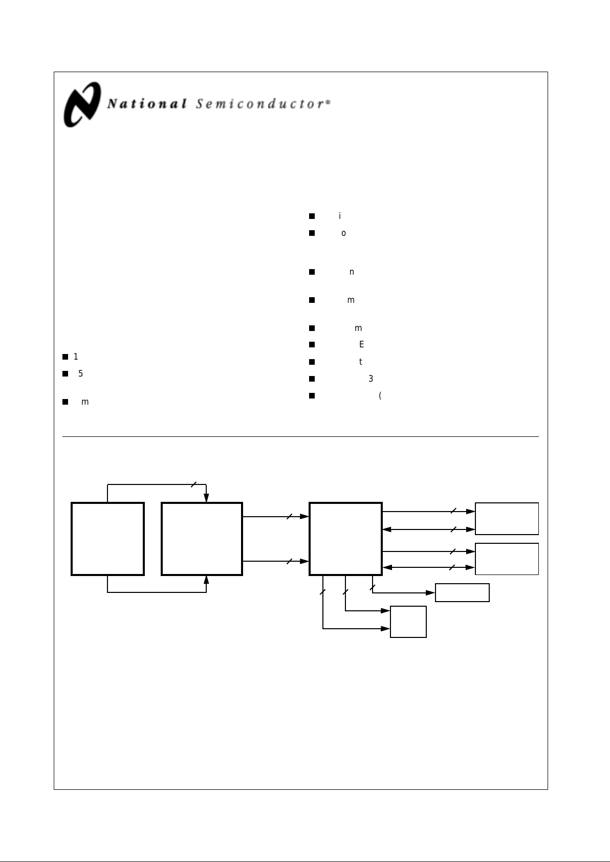
DSTN flat panels up to a 1024x768 resolution. The system connection example shows how the CS9210 interfaces with the rest of the system components.
Features
18-bit color support for digital pixel input
65 MHz pixel clock operation supports up to 1024x768
panels
SimultaneousCRTand DSTN display with up to 75 Hz
refresh rate
2X display refresh modes, up to 120 Hz
Supports most SVGA DSTN panels and the VESA
FPDI (Flat Panel Display Interface) Revision 1.0
Specification
TFT panel support provided by use of one connector;
allows a pass-through mode for the digital pixel input
Programmableframe rate modulation (FRM), up to 32
levels
Programmabledither, up to 16 levels
Supports EDO memory, 16-bit interface
Configuration via a serial programming interface
Low-power, 3.3V operation
144-pin LQFP (Low-profile Quad Flat Pack)
Geode™ CS9210 System Connection Example
DRAM Data
Addr Control
13
16
LCD Power
3
Control
Clocks
316
Panel Data
DSTN
PixelPort
24
PixelData
LCD
18
Geode™
GXm
Geode™
Geode™
CS9210
Graphics
CS5530
DRAM-B
256Kx16 bit
or
GXLV
Processor
DRAM-A
256Kx16 bit
Addr Control
13
DRAM Data
16
4
Serial
Configuration
I/O
Companion
Companion
Video Port (YUV)
National Semiconductor is a registered trademark of National Semiconductor Corporation.
Geode is a trademark of National Semiconductor Corporation.
For a complete listing of National Semiconductor trademarks, please visit www.national.com/trademarks.
Page 2

www.national.com 2 Revision 3.2
Table of Contents
Geode™ CS9210
1.0 ArchitectureOverview..............................................3
2.0 SignalDefinitions..................................................4
2.1 PINASSIGNMENTS .......................................................4
2.2 SIGNALDESCRIPTIONS ...................................................8
2.2.1 PixelPortInterfaceSignals ...........................................8
2.2.2 SerialInterfaceSignals ..............................................9
2.2.3 FlatPanelInterfaceSignals ...........................................9
2.2.4 MemoryInterfaceSignals ...........................................10
2.2.5 ResetandInternalTestPins .........................................11
2.2.6 PowerandGroundPins .............................................11
3.0 Functional Description . . . . . . . . . . . . . . . . . . . . . . . . . . . . . . . . . . . . . . . . . . . . 12
3.1 MODESELECTION .......................................................12
3.2 2XREFRESHMODE ......................................................14
3.3 TIMINGSIGNALSANDPANELCLOCK .......................................15
3.4 SIMULTANEOUSDISPLAY .................................................15
3.5 MAXIMUMFREQUENCY...................................................16
3.6 RESET PROCEDURES . . . . . . . . ............................................16
3.7 SERIALINTERFACE ......................................................16
3.8 COLORGENERATION ....................................................18
3.8.1 FrameRateModulation(FRM)........................................18
3.8.1.1 ChoosingFRMSequences ..........................................18
3.8.1.2 RemovalofFlickering ..............................................20
3.8.2 Dithering.........................................................20
3.8.2.1 N-BitDitheringSchemes ............................................21
3.8.3 CombiningFRMandDithering........................................22
3.8.3.1 ModifiedFRMandDithering .........................................22
3.9 PROGRAMMINGTHEFRMANDDITHERMEMORIES...........................22
3.9.1 AddressingtheFRMMemories .......................................22
3.9.2 AddressingtheDitheringMemories....................................23
4.0 RegisterDescriptions .............................................24
5.0 ElectricalSpecifications ...........................................30
5.1 ABSOLUTEMAXIMUMRATINGS............................................30
5.2 RECOMMENDEDOPERATINGCONDITIONS..................................30
5.3 DCCHARACTERISTICS ..................................................31
5.4 ACCHARACTERISTICS ...................................................32
5.4.1 PixelPortTiming ..................................................33
5.4.2 SerialInterfaceTiming ..............................................34
5.4.3 FlatPanelTiming ..................................................35
5.4.4 MemoryInterfaceTiming ...........................................36
6.0 MechanicalPackageOutline .......................................37
Appendix A Support Documentation . . . . . . . . . . . . . . . . . . . . . . . . . . . . . . . . . . . . 38
A.1 REVISIONHISTORY ......................................................38
Page 3
Revision 3.2 3 www.national.com
Geode™ CS9210
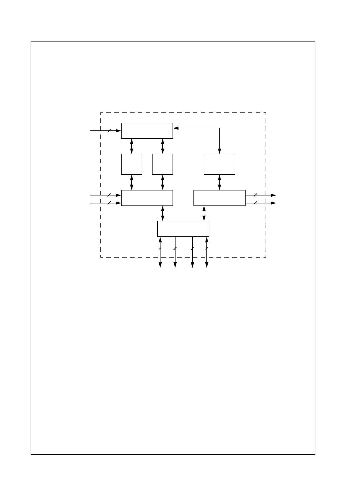
1.0 Architecture Overview
The major functional blocks, as shown in Figure 1-1, of
the Geode CS9210 graphics companion:
• Serial Interface
• DitherMemory
• FRM Memory
• Control Registers
• DSTN Formatter
• Display Controller
• DRAM Controller
Figure 1-1. Internal Block Diagram
Serial Interface
DSTN Formatter
Dither
Memory
FRM
Memory
Control
Registers
Display Controller
DRAM Controller
Pixel Control
6
Pixel Data
18
Serial Configuration
4
Panel Control
Panel Data
6
16
13 13
DRAM
Bank A
DRAM
Bank B
16 16
DRAM Data
DRAM Data
Addr Ctrl
Addr Ctrl
Page 4
www.national.com 4 Revision 3.2
Geode™ CS9210
2.0 Signal Definitions
This section defines the signals and external interface of
the Geode CS9210. Figure 2-1 shows the pins organized
by their functional groupings (internal test and electrical
pins are not shown).
2.1 PIN ASSIGNMENTS
The tables in this section use several common abbreviations. Table 2-1 lists the mnemonics and their meanings.
Figure 2-2 shows the pin assignment for the CS9210 with
Tables 2-2 and 2-3 listing the pin assignments sorted by
pin number and alphabetically by signal name, respectively.
In Section 2.2 “Signal Descriptions” a description of each
signal within its associated functional group is provided.
Figure 2-1. CS9210 S ignal Groups
Table 2-1. Pin Type Definitions
Mnemonic Definition
I Standard input pin.
I/O Bidirectional pin.
O Totem-pole output.
OD Open-drain output structure that
allows multiple devices to share the
pin in a wired-OR configuration
PU Pull-up resistor
PD Pull-down resistor
smt Schmitt Trigger
t/s Tri-state signal
VDD (PWR) Power pin.
VSS (GND) Ground pin
# The "#" symbol at the end of a signal
name indicates that the active or
asserted state occurswhen the signal
is at a lowvoltage level.When "#" is
not present after the signal name, the
signal is asserted when at a highvolt-
age level.
RED[5:0]
GREEN[5:0]
BLUE[5:0]
ENA_DISP
ENA_VDDIN
ENA_LCDIN
DOTCLK
FP_HSYNC
FP_VSYNC
SCLK
SDIN
SCS
SDO
LP
SHFCLK
FLM
UD[11:0]
LD[11:0]
DISPOFF#
FP_VDDEN
FP_VCONEN
MA_A[9:0]
MD_A[15:0]
MA_B[9:0]
MD_B[15:0]
OEA#
OEB#
RASA#
RASB#
LCASA#
UCASA#
LCASB#
UCASB#
RESET#
Memory
Interface
Reset
Interface
Flat Panel
Interface
Pixel Port
Interface
Geode™ CS9210
Graphics
Serial
Interface
WEA#
WEB#
Companion
Page 5
Revision 3.2 5 www.national.com
Signal Definitions (Continued)
Geode™ CS9210
Figure 2-2. 144-Pin LQFP Pin A ssignment Diagram
Order Number: CS9210-VNG
1
2
3
4
5
6
7
8
9
10
11
12
13
14
15
16
17
18
19
20
21
22
23
24
25
26
27
28
29
30
31
32
33
34
35
36
3738394041424344454647484950515253545556575859606162636465666768697071
72
108
107
106
105
104
103
102
101
100
99
98
97
96
95
94
93
92
91
90
89
88
87
86
85
84
83
82
81
80
79
78
77
76
75
74
73
144
143
142
141
140
139
138
137
136
135
134
133
132
131
130
129
128
127
126
125
124
123
122
121
120
119
118
117
116
115
114
113
112
111
110
109
Geode™ CS9210
Graphics Companion
VDD
VSS
FP_HSYNC
GREEN1
GREEN2
GREEN3
GREEN4
GREEN5
RED0
RED1
RED2
RED3
RED4
RED5
SCLK
SDIN
VDD
VSS
VSS
DOTCLK
SCS
SDO
MA_A9
MA_A8
MA_A7
MA_A6
MA_A5
MA_A4
MA_A3
MA_A2
MA_A1
MA_A0
MD_A15
MD_A14
MD_A13
VDD
VDD
VSS
MD_B6
MD_B5
MD_B4
MD_B3
MD_B2
MD_B1
MD_B0
OEB#
UCASB#
LCASB#
RASB#
WEA#
RASA#
LCASA#
VDD
VSS
OEA#
UCASA#
MD_A0
MD_A1
MD_A2
MD_A3
MD_A4
MD_A5
MD_A6
MD_A7
MD_A8
MD_A9
MD_A10
MD_A11
MD_A12
VSS
VDD
VDD
LD11
LD10
LD9
LD8
LD7
LD6
LD5
LD4
LD3
LD2
LD1
LD0
MA_B9
MA_B8
MA_B7
MA_B6
VDD
VSS
VSS
MA_B5
MA_B4
MA_B3
MA_B2
MA_B1
MA_B0
MD_B15
MD_B14
MD_B13
MD_B12
MD_B11
MD_B10
MD_B9
MD_B8
MD_B7
VDD
VSS
SHFCLK
UD0
UD1
UD2
UD3
UD4
UD5
UD6
UD7
UD8
UD9
UD10
UD11
FLM
TEST
VDD
VSS
LP
VSS
FP_VCONEN
FP_VDDEN
DISPOFF#
RESET#
ENA_LCDIN
ENA_VDDIN
ENA_DISP
BLUE0
BLUE1
BLUE2
BLUE3
BLUE4
BLUE5
GREEN0
FP_VSYNC
VDD
WEB#
Top View
Page 6
www.national.com 6 Revision 3.2
Signal Definitions (Continued)
Geode™ CS9210
Table 2-2. Pin Assignments - Sorted by P in Number
Pin
No. Signal Name Type
Drive
(mA)
1VDD PWR -2 VSS GND -3 F P_HSYNC I -4GREEN1 I -5GREEN2 I -6GREEN3 I -7GREEN4 I -8GREEN5 I --
9RED0 I -10 RED1 I -11 RED2 I -12 RED3 I -13 RED4 I -14 RED5 I -15 SCLK I -16 SDIN I -17 VDD PWR -18 VSS GND -19 VSS GND -20 DOTCLK I -21 SCS I -22 SDO O 6
23 MA_A9 O 4
24 MA_A8 O 4
25 MA_A7 O 4
26 MA_A6 O 4
27 MA_A5 O 4
28 MA_A4 O 4
29 MA_A3 O 4
30 MA_A2 O 4
31 MA_A1 O 4
32 MA_A0 O 4
33 MD_A15 I/O 4
34 MD_A14 I/O 4
35 MD_A13 I/O 4
36 VDD PWR --
37 VDD PWR -38 VSS GND -39 MD_A12 I/O 4
40 MD_A11 I/O 4
41 MD_A10 I/O 4
42 MD_A9 I/O 4
43 MD_A8 I/O 4
44 MD_A7 I/O 4
45 MD_A6 I/O 4
46 MD_A5 I/O 4
47 MD_A4 I/O 4
48 MD_A3 I/O 4
49 MD_A2 I/O 4
50 MD_A1 I/O 4
51 MD_A0 I/O 4
52 UCASA# O 4
53 OEA# O 4
54 VSS GND -55 VDD PWR -56 LCASA# O 4
57 RASA# O 4
58 WEA# O 4
59 WEB# O 4
60 RASB# O 4
61 LCASB# O 4
62 UCASB# O 4
63 OEB# O 4
64 MD_B0 I/O 4
65 MD_B1 I/O 4
66 MD_B2 I/O 4
67 MD_B3 I/O 4
68 MD_B4 I/O 4
69 MD_B5 I/O 4
70 MD_B6 I/O 4
71 VSS GND -72 VDD PWR --
Pin
No. Signal Name Type
Drive
(mA)
73 VDD PWR -74 MD_B7 I/O 4
75 MD_B8 I/O 4
76 MD_B9 I/O 4
77 MD_B10 I/O 4
78 MD_B11 I/O 4
79 MD_B12 I/O 4
80 MD_B13 I/O 4
81 MD_B14 I/O 4
82 MD_B15 I/O 4
83 MA_B0 O 4
84 MA_B1 O 4
85 MA_B2 O 4
86 MA_B3 O 4
87 MA_B4 O 4
88 MA_B5 O 4
89 VSS GND -90 VSS GND -91 VDD PWR -92 MA_B6 O 4
93 MA_B7 O 4
94 MA_B8 O 4
95 MA_B9 O 4
96 LD0 O 12
97 LD1 O 12
98 LD2 O 12
99 LD3 O 12
100 LD4 O 12
101 LD5 O 12
102 LD6 O 12
103 LD7 O 12
104 LD8 O 12
105 LD9 O 12
106 LD10 O 12
107 LD11 O 12
108 VDD PWR --
Pin
No. Signal Name Type
Drive
(mA)
109 VSS GND -110 SHFCLK O 12
111 UD0 O 12
112 UD1 O 12
113 UD2 O 12
114 UD3 O 12
115 UD4 O 12
116 UD5 O 12
117 UD6 O 12
118 UD7 O 12
119 UD8 O 12
120 UD9 O 12
121 UD10 O 12
122 UD11 O 12
123 FLM O 12
124 TEST I -125 VDD PWR -126 VSS GND -127 LP O 12
128 VSS GND -129 FP_VCONEN O 12
130 FP_VDDEN O 1 2
131 DISPOFF# O 12
132 RESET# I -133 ENA_LCDIN I -134 ENA_VDDIN I -135 ENA_DISP I -136 BLUE0 I -137 BLUE1 I -138 BLUE2 I -139 BLUE3 I -140 BLUE4 I -141 BLUE5 I -142 GREEN0 I -143 FP_VSYNC I -144 VDD PWR --
Pin
No. Signal Name Type
Drive
(mA)
Page 7
Revision 3.2 7 www.national.com
Signal Definitions (Continued)
Geode™ CS9210
Table 2-3. Pin Assignments - Sorted Alphabetically by Signal Name
Signal Name
Pin
No.
BLUE0
136
BLUE1 137
BLUE2 138
BLUE3 139
BLUE4 140
BLUE5 141
DISPOFF# 131
DOTCLK 20
ENA_DISP 135
ENA_LCDIN 133
ENA_VDDIN 134
FLM 123
FP_HSYNC 3
FP_VCONEN 129
FP_VDDEN 130
FP_VSYNC 143
GREEN0 142
GREEN1 4
GREEN2 5
GREEN3 6
GREEN4 7
GREEN5 8
LCASA# 56
LCASB# 61
LD0 96
LD1 97
LD10 106
LD11 107
LD2 98
LD3 99
LD4 100
LD5 101
LD6 102
LD7 103
LD8 104
LD9 105
LP 127
MA_A0 32
MA_A1 31
MA_A2 30
MA_A3 29
MA_A4 28
MA_A5 27
MA_A6 26
MA_A7 25
MA_A8 24
MA_A9 23
MA_B0 83
MA_B1 84
MA_B2 85
MA_B3 86
MA_B4 87
MA_B5 88
MA_B6 92
MA_B7 93
MA_B8 94
MA_B9 95
MD_A0 51
MD_A1 50
MD_A2 49
MD_A3 48
MD_A4 47
MD_A5 46
MD_A6 45
MD_A7 44
MD_A8 43
MD_A9 42
MD_A10 41
MD_A11 40
MD_A12 39
MD_A13 35
MD_A14 34
Signal Name
Pin
No.
MD_A15 33
MD_B0 64
MD_B1 65
MD_B2 66
MD_B3 67
MD_B4 68
MD_B5 69
MD_B6 70
MD_B7 74
MD_B8 75
MD_B9 76
MD_B10 77
MD_B11 78
MD_B12 79
MD_B13 80
MD_B14 81
MD_B15 82
OEA# 53
OEB# 63
RASA# 57
RASB# 60
RED0 9
RED1 10
RED2 11
RED3 12
RED4 13
RED5 14
RESET# 132
SCLK 15
SCS 21
SDIN 16
SDO 22
SHFCLK 110
TEST 124
UCASA# 52
UCASB# 62
Signal Name
Pin
No.
UD0 111
UD1 112
UD2 113
UD3 114
UD4 115
UD5 116
UD6 117
UD7 118
UD8 119
UD9 120
UD10 121
UD11 122
VDD 1
VDD 17
VDD 36
VDD 37
VDD 55
VDD 72
VDD 73
VDD 91
VDD 108
VDD 125
VDD 144
VSS 2
VSS 18
VSS 19
VSS 38
VSS 54
VSS 71
VSS 89
VSS 90
VSS 109
VSS 126
VSS 128
WEA# 58
WEB# 59
Signal Name
Pin
No.
Page 8

www.national.com 8 Revision 3.2
Signal Definitions (Continued)
Geode™ CS9210
2.2 SIGNAL DESCRIPTIONS
2.2.1 Pixel Port Interface Signals
Signal Name Pin No.
Type
(Drive) Description
RED[5:0] 14-9 I Red Pixel Channel
These six pins are the red component of the pixel port input. The six
most significant bits of the CS5530 pixel port (FP_DATA[17:12] on an
18-bit pixel port) are connected to these pins. RED5 is the MSB (most
significant bit) and RED0 is the LSB (least significant bit).
GREEN[5:0] 8-4,142 I Green Pixel Channel
These six pins are the green component of the pixelport input. The six
middle bits of the CS5530 pixel port (FP_DATA[11:6] on an 18-bit pixel
port) are connected to these pins. GREEN5 is theMSB and GREEN0
is the LSB.
BLUE[5:0] 141-136 I Blue Pixel Channel
These six pins are the bluecomponent of the pixel port input. The six
least significant bits of the CS5530 pixel port (FP_DATA[5:0]on an 18bit pixel port) are connected to these pins. BLUE5 is the MSB and
BLUE0 is the LSB.
ENA_DISP 135 I Active Display Enable
This input is asserted when the pixel data stream is presenting valid
displaydata to the pixel port.
ENA_VDDIN 134 I Input VDD Enable
When this input is asserted, it indicates that the display controller in
the CS9210 should apply voltage to the LCD panel.
ENA_LCDIN 133 I Input LCD Enable
When this input is asserted, it indicates that the display controller in
the CS9210 should drive valid control signals to the LCD panel.
DOTCLK 20 I Dot Clock
This signal is the pixel clock from thevideo controller. It is used to
clock data in from thepixel port. Additionally, this signal is used as the
inputclock forthe entire CS9210device.This clock must be running at
all times after reset for the CS9210 to function correctly.
FP_HSYNC 3 I Flat Panel Horizontal Sync Input
When the input data stream is in a horizontal blanking period, this
input is asserted. It is a pulse that isused to synchronize displaylines
and to indicate when the pixel data stream is not valid due to blanking.
FP_VSYNC 143 I Flat Panel Vertical Sync Input
When the input data stream is in a vertical blanking period, this inputis
asserted. It is a pulse used to synchronize display frames and toindicate when the pixel data stream is not valid due to blanking.
Page 9

Revision 3.2 9 www.national.com
Signal Definitions (Continued)
Geode™ CS9210
2.2.2 Serial Interface Signals
Signal Name Pin No.
Type
(Drive) Description
SCLK 15 I Serial Interface Clock
This input signal is the clock for the serial controlinterface. The other
serial interface signals (SDIN, SCS, SDO) are synchronous to this signal.
SDIN 16 I Serial Data Input
This is the data input line for the serial control interface. Input data is
serializedon this pin, including the commandstream forregister reads
and writes.
SDO 22 O
(6 mA)
Serial Data Output
This is the data output line for the serial control interface. Output data
is serialized on this pin in response to register read commands.
SCS 21 I Serial Chip Select
This active high chipselect indicates when valid data is being clocked
in or out via the SDIN/SDO pins.
2.2.3 Flat Panel Interface Signals
Signal Name Pin No.
Type
(Drive) Description
LP 127 O
(12 mA)
Latch Pulse
This is the line pulseor latch pulsefor the flat panel data,indicating
the output data is notvalid, a display line has endedand another is
about to start.
Depending on the type of panel beinginterfaced, this signal can also
be referred to as CL1 or LINE.
SHFCLK 110 O
(12 mA)
Panel Clock (Shift Clock)
This is the shift clock or pixelclock for the flat panel data. This signal is
used to clock pixel data into the LCD panel.
Depending on the type of panel beinginterfaced, this signal can also
be referred to as CL2 or SHIFT.
FLM 123 O
(12 mA)
First Line Marker
This is the frame pulse for the flat panel data indicating the output data
is not valid, and one display frame has ended and another is about to
start.
Depending on the type of panel beinginterfaced, this signal can also
be referred to as FP or FRAME.
UD[11:0] 122-111 O
(12 mA)
Upper Scan Data
These outputs are the upper panel pixel data bus to the DSTN LCD
panel. Its format is dependent on thedisplay mode configured for the
LCD panel. Refer to Section 3.1 “ModeSelection” on page 12.
LD[11:0] 107-96 O
(12 mA)
Lower Scan Data
These outputs are the lower panel pixel data bus to the DSTN LCD
panel. Its format is dependent on thedisplay mode configured for the
LCD panel. Refer to Section 3.1 “ModeSelection” on page 12.
Page 10

www.national.com 10 Revision 3.2
Signal Definitions (Continued)
Geode™ CS9210
DISPOFF# 131 O
(12 mA)
Disables Panel
When this output is asserted low, it indicates that the LCD panel
should be disabled.
FP_VDDEN 130 O
(12 mA)
Controls LCD VDD FET
When this output is asserted high, voltage should be applied to the
panel. This signal is intended to controla power FET to the LCD
panel.
FP_VCONEN 129 O
(12 mA)
Controls LCD Bias Voltage Enable
When this output is asserted high, the contrast voltage(VCON) should
be applied to the panel.
2.2.3 Flat Panel Interface Signals (Continued)
Signal Name Pin No.
Type
(Drive) Description
2.2.4 Memory Interface Signals
Signal Name Pin No.
Type
(Drive) Description
MA_A[9:0] 23-32 O
(4 mA)
DRAM Bank A Address Bus
The address bus for Bank A of the DRAM.
MD_A[15:0] 33-35,
39-51
I/O
(4 mA)
DRAM Bank A Data Bus
The data bus for Bank A of the DRAM.
MA_B[9:0] 95-92,
88-83
O
(4 mA)
DRAM Bank B Address Bus
The address bus for Bank B of the DRAM.
MD_B[15:0] 82-74,
70-64
I/O
(4 mA)
DRAM Bank B Data Bus
The data bus for Bank B of the DRAM.
OEA# 53 O
(4 mA)
DRAM Bank A Output Enable
The output enable for Bank A of the DRAM.
OEB# 63 O
(4 mA)
DRAM Bank B Output Enable
The output enable for Bank B of the DRAM.
RASA# 57 O
(4 mA)
DRAM Bank A Row Address Strobe
The row address strobe for Bank A of the DRAM.
RASB# 60 O
(4 mA)
DRAM Bank B Row Address Strobe
The row address strobe for Bank B of the DRAM.
UCASA# 52 O
(4 mA)
DRAM Bank A High Byte Column Address Strobe
The column address strobe for the upper eight bits of data for Bank A
of the DRAM.
LCASA# 56 O
(4 mA)
DRAM Bank A Low Byte Column Address Strobe
The column address strobe for the lower eight bits of data for Bank A
of the DRAM.
UCASB# 62 O
(4 mA)
DRAM Bank B High Byte Column Address Strobe
The column address strobe for the upper eight bits of data for Bank B
of the DRAM.
Page 11

Revision 3.2 11 www.national.com
Signal Definitions (Continued)
Geode™ CS9210
LCASB# 61 O
(4 mA)
DRAM Bank B Low Byte Column Address Strobe
The column address strobe for the lower eight bits of data for Bank B
of the DRAM.
WEA# 58 O
(4 mA)
DRAM Bank A Write Enable
The write enable signal for Bank A of the DRAM.
WEB# 59 O
(4 mA)
DRAM Bank B Write Enable
The write enable signal for Bank B of the DRAM.
2.2.4 Memory Interface Signals (Continued)
Signal Name Pin No.
Type
(Drive) Description
2.2.5 Reset and Internal Test Pins
Signal Name Pin No.
Type
(Drive) Description
RESET# 132 I Reset
This pin is the system reset input.
TEST 124 I Reserved
This pin must be tied to ground. It is a National Semiconductor internal
test mode pin only.
2.2.6 Power and Ground Pins
Signal Name Pin No.
Type
(Drive) Description
VDD 1, 17, 36,
37, 55,
72, 73,
91, 108,
125, 144
PWR Power Connection (total of 11 pins)
Power for the DRAM and system interface signals. These should be
supplied with 3.3V.
VSS 2, 18, 19,
38, 54,
71, 89,
90, 109,
126, 128
GND Ground Connection (total of 11 pins)
Ground connection.
Page 12
www.national.com 12 Revision 3.2
Geode™ CS9210
3.0 Functional Description
The Geode CS9210 graphics companion connects to the
TFT port of the CS5530 I/O companion chip (see Figure
3-1). It formats the graphics refresh data for the DSTN display and controls the refresh of the DSTNLCD.
The CS9210 must be connected to two 60ns EDO
(Extended Data Out) 256Kx16 DRAMs that store a DSTNformatted copy of the frame buffer. Pixel data is received
by the pixel port, formatted by a programmable FRM
(Frame Rate Modulator) and dither block, and then stored
in the CS9210 frame buffer. The formatted pixel data is
subsequently read from the DRAMs and used to refresh
the DSTN panel. The panel can be refreshed at 1X or 2X
the input refresh rate, up to a maximum refresh rate of
120Hz.UsingtwobanksofDRAM,theCS9210controls
each bank independently to allow for maximal use of the
DRAM bandwidth and to minimize the amount of on-chip
buffering.
The FRM/dithering formatting is accomplished via a pair
of mapping RAMs. The first is used for FRM coloring; the
second for dithering. The FRM RAM is a 32x64-bit map,
representing 64 frames of data for 32 color patterns. The
dithering RAM is a 16x4x4-bit map, yielding 16 dithering
levels. The RAM-based FRM/dither approach gives the
OEM the most flexibility to tune the FRM and dithering
algorithms for a specificpanel.
The FRM and dither maps are loaded, along with the
remaining control registers, through a simple serial programming port that connects to the CS5530 I/O companionchipasillustratedinFigure3-1.Figure3-2showsan
alternative connection method.
3.1 MODE SELECTION
The CS9210 can be configured for three modes of operation. The mode selected depends on the type of panel
being connected to the flat panelinterface:
• 16-bit DSTN Mode
- Supports DSTN panels with 640x480or 800x600
resolutions.
• 24-bit DSTN Mode
- Supports DSTN panels with 1024x768 pixel resolution.
• TFT Pass-Through Mode
- Allows a common connector to be used for TFT LCD
panels and DSTN LCD panels.The system software
can configure the CS9210 to operate in a PassThrough mode that presents the digitalpixel (RGB)
input data on the UD/LD output pins to drive a TFT
panel on the common connector. The input data is
registered internally before being presented at the
output pins to better c ontrol the timing of the panel
interface signals.
Mode selection is programmed via Index 02h, bits 1 and 0
as shown in Table 3-1. Depending on the mode selected,
the panel data that is presented on the UD/LD buses will
vary.
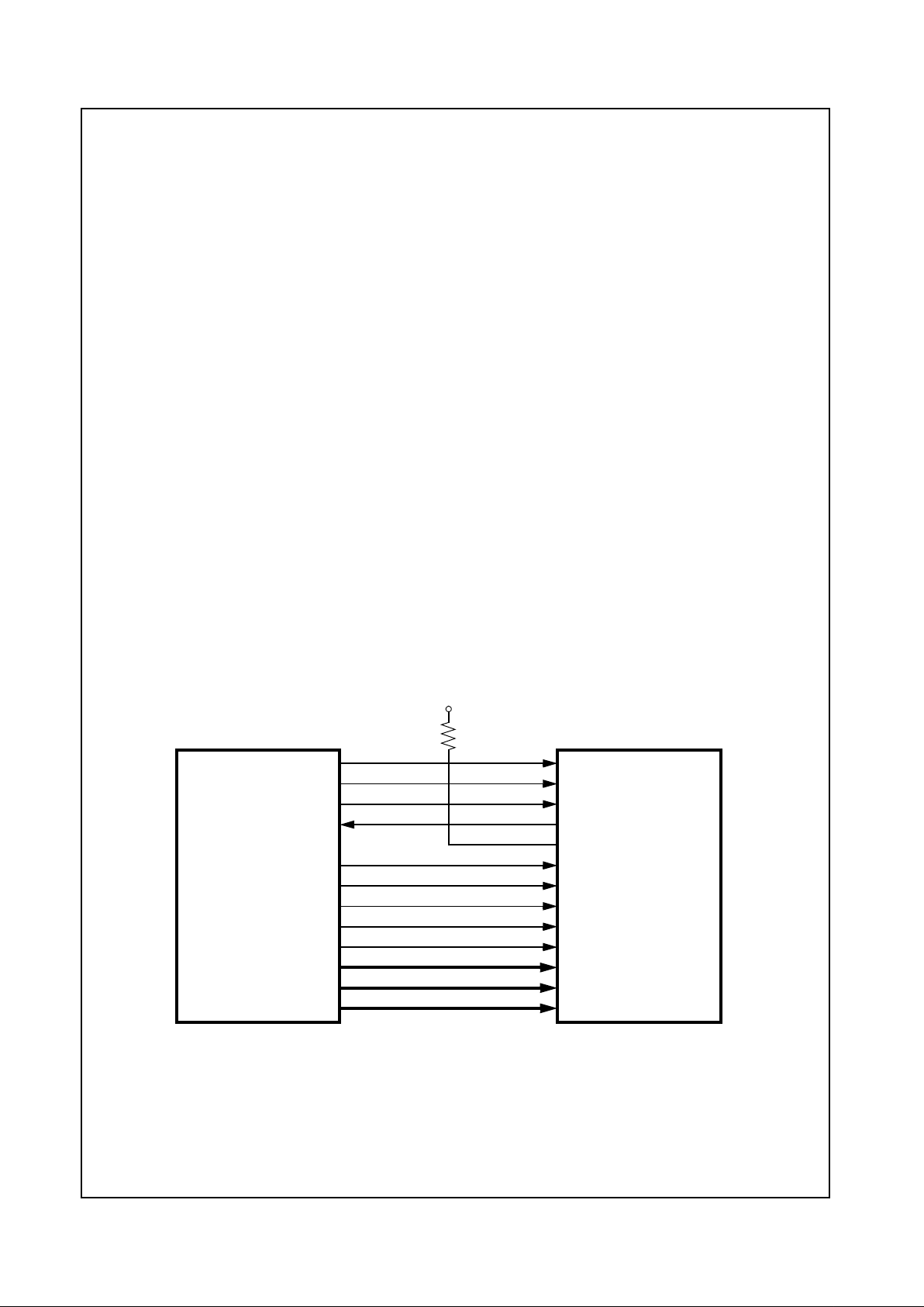
Figure 3-1. CS5530 and CS9210 Signal Connections
GPIOx
GPIOx
GPIOx
GPIOx
FP_ENA_VDD
FP_DISP_ENA_OUT
FP_CLK
FP_HSYNC
FP_VSYNC
FP_DATA[5:0]
FP_DATA[11:6]
FP_DATA[17:12]
SCLK
SDIN
SCS
SDO
ENA_LCDIN
ENA_VDDIN
ENA_DISP
DOTCLK
FP_HSYNC
FP_VSYNC
BLUE[5:0]
GREEN[5:0]
RED[5:0]
Geode™
VCC3
Geode™
CS5530 I/O
CS9210
Companion
Graphics
Companion
Page 13

Revision 3.2 13 www.national.com
Functional Description (Continued)
Geode™ CS9210
Figure 3-2. Connection Method Using Input Expansion Buffer
Table 3-1. Mode Selection Bits
Bit Description
Index 02h Control Register (R/W) Reset Value = 00h
1 16/24-Bit DSTN Select: UD/LD[11:0] formatted for: 0 = 16-bit (640x480 and 800x600), 1 = 24-bit (1024x768).
For this bit to beapplicable, bit 0 must = 0. Also see Section 3.1 “M ode Selection” on page 12.
0 Pass-through: UD/LD[11:0] are formatted for: 0 = DSTN, 1 = TFT Pass-through.
A setting of 1 overrides bit 1. See Section 3.1 “Mode Selection” onpage 12.
IOR#
SD[15:0]
FP_ENA_VDD
FP_DISP_ENA_OUT
FP_CLK
FP_HSYNC
FP_VSYNC
FP_DATA[5:0]
FP_DATA[11:6]
FP_DATA[17:12]
SCLK
SDIN
SCS
SDO
ENA_LCDIN
ENA_VDDIN
ENA_DISP
DOTCLK
FP_HSYNC
FP_VSYNC
BLUE[5:0]
GREEN[5:0]
RED[5:0]
VCC3
Input Expansion Buffer
GPCS#
GPIOx
GPIOx
GPIOx
ISA Bus
Geode™
CS5530 I/O
Companion
Geode™
CS9210
Graphics
Companion
Page 14

www.national.com 14 Revision 3.2
Functional Description (Continued)
Geode™ CS9210
Table 3-2 shows the mapping of the data in the three supported modes. The notation "UG1", for example, represents the bit value for the green component of pixel
number 1 for the upper panel data. Note that exactly 2 and
2/3 pixels are presented to the panel per SHFCLK in 16bit DSTN mode. The 16-bit DSTN mode pixel data
sequence shown in Table 3-2 would start on the next
SHFCLK with UB2 and LB2 followed by the bit values for
the red, green, and blue components of pixel 3.
The mode selection is dictated by the panel type. A panel
with a 1024x768 pixel resolution cannot be madeto run at
an 800x600 resolution by changing the mode selection
from 24-bit DSTN to 16-bit DSTN.
Also note that the 16-bit/24-bit designation applies to the
width of the data presented every SHFCLK to the DSTN
panel on the UD/LD outputs. The 16-bit/24-bit designation
has nothing to do with bits-per-pixel.
3.2 2X REFRESH MODE
When 2X refresh mode is enabled, each incoming frame
of screen data is duplicated or displayedtwice on the LCD
panel. The rate at which frames are displayed to the panel
is twice the incoming frame rate. Higher refresh rates
improve picture quality and help to reduce any flickering
effects caused by frame rate modulation.
Table 3-2. Panel Output Signal Mapping
Note: An "Unused" panel output is drivenlow at alltimes.
LCD
Outputs
16-Bit
DSTN
24-Bit
DSTN
TFT Pass-
Through
Mode
UD11 Unused UR0 Unused
UD10 Unused UG0 Unused
UD9 Unused UB0 Unused
UD8 Unused UR1 Unused
UD7 UR0 UG1 RED0
UD6 UG0 UB1 RED1
UD5 UB0 UR2 RED2
UD4 UR1 UG2 GREEN0
UD3 UG1 UB2 BLUE2
UD2 UB1 UR3 RED3
UD1 UR2 UG3 GREEN3
UD0 UG2 UB3 BLUE3
LD11 Unused LR0 Unused
LD10 Unused LG0 Unused
LD9 Unused LB0 BLUE5
LD8 Unused LR1 GREEN5
LD7 LR0 LG1 GREEN1
LD6 LG0 LB1 GREEN2
LD5 LB0 LR2 BLUE0
LD4 LR1 LG2 BLUE1
LD3 LG1 LB2 RED4
LD2 LB1 LR3 GREEN4
LD1 LR2 LG3 BLUE4
LD0 LG2 LB3 RED5
LP LP LP FP_HSYNC
FLM FLM FLM FP_VSYNC
SHFCLK SHFCLK SHFCLK DOTCLK
DISPOFF# DISPOFF# DISPOFF# ENA_DISP
FP_VDDEN FP_VDDEN FP_VDDEN ENA_VDDIN
FP_VCONEN FP_VCONEN FP_VCONEN ENA_LCDIN
Page 15

Revision 3.2 15 www.national.com
Functional Description (Continued)
Geode™ CS9210
3.3 TIMING SIGNALS AND PANEL CLOCK
The CS9210 controls the generation of the flat panel timing signals via internal counters that count pixels as they
are output to the display. When the last pixel of a line is
output, the LP signal is asserted. The duration of the LP is
programmable via the LP Start and End registers at Index
0Ch-0Fh has shown in Table 3-3. Certain panels require
extra LPs at the end of a frame scan. This requirement is
also suppor ted. The FLM output is asserted after a vertical sync has occurred and the first pixel line, while
ENA_DISP is active, has begun. Position and duration of
the FLM pulse is also programmable via the FLM Start
and End registers at Index 10h-13h as shown in Table 3-3.
The CS9210 generates the STN panel clock. Since fractional pixels are generally sent on the pixel bus to STN
panels,the ability to control the SHFCLK signal on a pixelto-pixel basis is providedto modulate the panel clock duty
cycle. Generally, for 16-bit DSTNs, the panel clock is the
DOTCLK divided by four with every fourth pulse masked
off (three SHFCLKs for four DOTCLK/4s). Programmable
options provide support for a wide rangeof panels.
3.4 SIMULTANEOUS DISPLAY
TheproblemwithdisplayingpixeldatatobothaCRT
screen and a dual-scan STN panel at the same time, is
that both the upper and lower halves of a dual-scan STN
panel screen must be written at the same time. Fora dualscan STN panel, pixel data for two horizontal scan lines is
written to the panel at the same time, one scan line to the
upper half of the panel and one scan line to the lower half
of the panel. This differs from the order that pixel data is
written to a CRT screen, where the pixel data for one horizontal scan line at a time is written to the screen, starting
with the scan line at the top of the screen and ending at
the bottom of the screen.
Designs which incorporate the CS9210 are able to support simultaneous display with a dual-scan STN panel and
CRT. The CS9210 stores an entire frame of pixel data in
one of the external DRAM frame buffers, and then reorders the pixel data stream to include pixel data for both
the upper and lower halves of the screen before sending
the data out to the panel. The data in the DRAM buffer
has already been frame-rate-modulatedand/or dithered, if
necessary, and packed as three bits per pixel.
Simultaneous display is supported with both the panel
and CRTin the same mode and refresh rate. In this mode,
the refresh rate should be set as high as possible while
maintaining compatibility with established monitor timing
standards (typically 72-75 Hz). The same pixel input data
is fed to the CRT and the CS9210 simultaneously. As the
data comes into the CS9210, it is stored in one of the
externalDRAMframebuffers.Atthesametimedatais
being stored for the current frame, the CS9210 is reading
pixel data for the previous frame from the other external
DRAM frame buffer and sending it out on the flat panel
interface.
Table 3-3. Timing Related Registers
Bit Description
Index 0Ch-0Dh LP Start Register (R/W) Reset Value = 005Ah
15:12 Reserved: M u st be set to 0.
11:0 LP Start: 12-bit value that specifies the number of DOTCLK cycles to the star t of the next LP pulse from the falling edge
of the last LP before internal VSYNC. (Refer to Figure 4-1.)
Index 0Eh-0Fh LP End Register (R/W) Reset Value = 0075h
15:12 Reserved: M u st be set to 0.
11:0 LP End: 12-bit value that specifies the number of DOTCLK cycles in duration for updating one line of the LCD panel. This
value is used only in 1X Refresh Mode (Index02h[5] = 0). (Refer to Figure 4-1.)
Index 10h-11h FLM Start Register (R/W Reset Value = 0020h
15:12 Reserved: M u st be set to 0.
11:0 FLM Start — 12-bit value that specifies t he number of DOTCLK cycles to the start of an FLM pulse from the inter nal
VSYNC signal rising edge. (Refer to Figure 4-1.)
Index 12h-13h FLM End Registe r (R/ W ) Reset Value = 0010h
15:12 Reserved: M u st be set to 0.
11:0 FLM End: 12-bit value that specifies the number of DOTCLK cycles to the falling edge of the FLM pulse from the falling
edge of the first LP after the FLM pulse started. (Refer to Figure 4-1.)
Page 16

www.national.com 16 Revision 3.2
Functional Description (Continued)
Geode™ CS9210
3.5 MAXIMUM FREQUENCY
The CS9210 will operate at a DOTCLK frequency of up to
65 MHz. There is no minimum frequency for the CS9210
device;however, many flat panelshave signal timings that
require minimum frequencies. Refer to the flat panel display specifications as appropriate.
3.6 RESET PROCEDURES
The SCLK and DOTCLK inputs do not need to be running
when RESET# is asserted low. The assertion of RESET#
or the issue of a soft reset through the serial interface will
force the CS9210 into an internal reset s tate. After
RESET# is deasserted or after a soft reset is issued, the
CS9210 requires four SCLK pulses followed by ten DOTCLK pulses to bring it out of the internal reset state.
3.7 SERIAL INTERFACE
The serial interfaceis used to read and write registers and
the FRM and dithering pattern memories inside the
CS9210. One byte at a time is transferred across the
serial interface. The serial interface protocol defines an 8bit address for up to 256 bytes of direct addressing. The
address mapping for this 256 byte address space is
defined in Table 4-1 on page 24.
As shown in Table 3-4, the Control Register, Index 02h,
which is accessed through this s erial interface, contains a
bit called LCD Enable (bit 6). This bit is turned on only
after all timing registers and FRM/Dither memories have
been programmed. The LCD panel will not power on until
this bit is enabled.
When this bit is enabled, all other registers accessed
through the serial interface become read only and cannot
be written to, and the FRM and dither memory address
ranges cannot be accessed at all. Writing to other registers or the FRM and dither memory addresses while the
LCD enable bit is enabled has no effect. Reading from the
FRM and dither memory address spaces while the LCD
enable bit is enabled returns unknown data.
Table 3-4. LCD Enable Bit
Bit Description
Index 02h Control Register (R/W) Reset Value = 00h
6 LCD Enable: This bit cannot be enabled until all timing registers and FRM/dither memories have been programmed. The
LCD panel will not display until t his bit is enabled.
0 = Disable, EN A_VDDIN input ignored and all LCD registers can be written.
1 = Enable, external ENA_VDDIN input still required to enable panel.
WARNING: When this bit is enabled, all registers except Index 02h and 03h are read only and the FRM and dither mem-
ory addresses cannot be re ad or written. Writing to these registers or the FRM and dither memories while this bit is
enabled will have no effect. Reading from the FRM and dither memories while this bit is enabled will retur n unknown data.
Page 17

Revision 3.2 17 www.national.com
Functional Description (Continued)
Geode™ CS9210
The read and write protocols for the serial interface are
described in Table 3-5 and illustrated in Figures 3-3 and 3-
4. The protocol begins with the assertion of the SCS
input, followed by one start bit and three command bits.
Only two commands are defined, one for read and onefor
write. The read protocol continues with one idle bit and
eightbitsofreaddataonSDO.Thewriteprotocolcontinues with eight bits of write data on SDIN and one idle bit.
The deassertion of the SCS input for one SCLK cycle is
required to end the transaction.
Note that data driven into the CS9210 is shown changing
on the falling edge of SCLK. In general, this is a good
practice to avoid hold time problems that might occur i f the
data were changing near the rising edge of SCLK. The
CS9210 samples the serial interface input signals with the
rising edge of SCLK. Data driven on the SDO output by
the CS9210 changes on the rising edge of SCLK.
Figure 3-3. Serial Interface Read Cycle Timing Diagram
Figure 3-4. Serial Interface Write Cycle Timing Diagram
Table 3-5. Serial Interface Read/Write Sequences
Cycle(s) Read Sequence with SCS = “1” Write Sequence with SCS = “1”
1 1 Start bit SDIN = “1” 1 Start bit SDIN = “1”
3 3 Command bits SDIN = “000” 3 Command bits SDIN = “001”
8 8 Address bits ex: SDIN ="01110100" 8 Address bits ex: SDIN = "01101001"
1 1 Idle bit SDIN = “0” 1 Idle bit SDIN = “0”
8 8 Read data bits ex: SDO = "10011010" 8 Wr ite data bits ex: SDIN = "10010011"
SCLK
SCS
SDO
SDIN
0 0 0 Address[7], [6],... [0]
Data[7], [6],... [0]
Hi-Z Tri-state
1
SCLK
SCS
SDO
SDIN
0 0 1 Address[7], [6],... [0]
Data[7], [6],... [0]
Hi-Z Tri-state
1
Page 18

www.national.com 18 Revision 3.2
Functional Description (Continued)
Geode™ CS9210
3.8 COLOR GENERATION
Each pixel on an LCD panel consists of three primary
color components: red, green, and blue. Each primary
color component, for a given pixel, can be either turned on
or turned off. A total of eight colorscan be generated for a
given pixel through different combinations of turning each
color component either on or off. In order to generate
more colors, frame rate modulation (FRM) and dithering
are used in theCS9210. The CS9210 is capable of generating 262,144 different colors based on the 18-bit RGB
pixel input from the pixel por t interface. The following sections describe how frame rate modulation and dithering
are implemented.
3.8.1 Frame Rate Modulation (FRM)
The idea of frame rate modulation is to turn each primary
color component of a pixel on and off at a certain rate to
create the perception of various color intensities. The
intensity or brightness of each color component depends
on what percentage of time the color component is turned
on and what percentage of time the color component is
turned off.
For example, take a given pixel whose blue and green
color components are always off. If the pixel’s red color
component was also always off, the pixel would be black.
If the pixel’sred color component was always on, the pixel
would be bright red, as bright as the red could get. However, if the red color component were alternating between
being on and off, the pixel would look about half as bright
as the brightest red.
The CS9210 independently turns the red, green, and blue
pixel color components on and off on a per frame basis (a
frame is one entire screen of pixels). The FRM sequence
specifieswhich frames the color component will be on and
which ones it will be off. These sequences are 64 bits
long, with each bit representing one frame. Once the end
of a sequence has been reached, the CS9210 will go
back to the beginning of the sequence and start over.
Figure 3-5 illustrates how one color component of a given
pixelmight be turned on and off over 64 frames to achieve
the perception of a given color component intensity.
The pixel port data of the CS9210 is comprised of six bits
for each of the three primary colors. Each of these 6-bit
color intensity values is dithered down to five bits (see
Section 3.8.2 “Dithering” on page 20 for a detailed
description of dithering). These 5-bit color intensity values
are then used to select one of the 32 FRM sequences
stored in the CS9210.
Figure 3-5. Sample FRM Sequence
3.8.1.1 Choosing FRM Sequences
Care must be taken when choosing FRM sequences to
reduce the effects of flickering (the low frequency variations) that can be detected by the human eye.Definition of
FRM sequences will also depend on the characteristics of
the LCD panel being used. For these reasons, generation
of an FRM sequence table involves lots of experimentation. Table 3-6 illustrates an FRM sequence table for a single primary color component.
An FRM sequence of 1’s and 0’s is defined for each 5-bit
input color component intensity value.The frequency ratio
indicates the number of 0 to 1 transitions within the 64
frame sequence. This value multiplied by the screen
refresh rate will give the frequency of frame rate modulation for the given color component intensity. The intensity
ratio indicates the fractional amount of time that the pixel
color component will be turned on.
Higher frame modulation frequencies result in better picture quality. Very low frequencies are more noticeable to
the human eye. It also seems that the human eye is less
responsiveto differences in frequency at low intensities.
The relationship between input intensity and the resulting
intensity ratio of the FRM sequence is not necessarily linear. This relationship depends on the non-linear characteristics of the LCD panel used.
1
0
1
1
1
0
0
Frame-count = 0
Frame-count = 1
Frame-count = 2
Frame-count = 3
Frame-count = 61
Frame-count = 62
Frame-count = 63
Page 19

Revision 3.2 19 www.national.com
Functional Description (Continued)
Geode™ CS9210
In the FRM Sequence Table it was determined through
experimentation that intensity ratios outside the range of
16/64 to 48/64 (other than 0/64 and 64/64) resulted in frequency ratios that were low enough that the human eye
would be able to detect flickering more easily. However,
because the human eye is less sensitive to frequency
variations at low intensity, instead of jumping directly from
0/64 to 16/64, it appeared acceptable to gradually
increase the intensity ratio from 0/64 to 16/64. The intensity ratio then slowly increases from 16/64 to 48/64 tocreate a smooth transition through different gray scale levels.
The full scale intensity ratio is truncated at 48/64 intentionally to reducethe effect of sudden changes in intensity
level and frequency v ariation.
Table 3-6. FRM Sequence Table Example For One Color Component
Input
Intensity Frame Count from 0 to 63
Freq.
Ratio
Intensity
Ratio
0 0000000000000000000000000000000000000000000000000000000000000000 0/64 0/64
1 0000000000000000000000000000000000000000000000000000000000000000 0/64 0/64
2 0000000100000001000000010000000100000001000000010000000100000001 8/64 8/64
3 0000001000001000000100000100000100000010000010000001000001000001 10/64 10/64
4 0001000100010001000100010001000100010001000100010001000100010001 16/64 16/64
5 0001001001001001001001001001001001001001001001001001001001001001 21/64 21/64
6 0010010010010100100100100101001001001010010010010010100100100101 23/64 23/64
7 0010010100100101001001010010010100100101001001010010010100100101 24/64 24/64
8 0010010100101001010010010100101001010010100100101001010010100101 25/64 25/64
9 0010100101001010010100101001010100101001010010100101001010010101 26/64 26/64
10 0010100101010010101001010010101001010100101001010100101010010101 27/64 27/64
11 0010101001010101001010100101010100101010010101010010101001010101 28/64 28/64
12 0010101010010101010100101010101001010101010010101010100101010101 29/64 29/64
13 0010101010101010010101010101010100101010101010100101010101010101 30/64 30/64
14 0010101010101010101010101010101001010101010101010101010101010101 31/64 31/64
15 0101010101010101010101010101010101010101010101010101010101010101 32/64 32/64
16 0101010101010101010101010101010110101010101010101010101010101011 31/64 33/64
17 0101010101010101101010101010101101010101010101011010101010101011 30/64 34/64
18 0101010101101010101011010101010110101010101101010101011010101011 29/64 35/64
19 0101010110101011010101011010101101010101101010110101010110101011 28/64 36/64
20 0101011010101101010110101101010110101011010110101011010101101011 27/64 37/64
21 0101011010110101101011010110101101010110101101011010110101101011 26/64 38/64
22 0101101011010110101101101011010110101101011011010110101101011011 25/64 39/64
23 0101101101011011010110110101101101011011010110110101101101011011 24/64 40/64
24 0101101101101011011011011010110110110101101101101101011011011011 23/64 41/64
25 0101101101101101101101101101101101011011011011011011011011011011 22/64 42/64
26 0110110110110110110110110110110110110110110110110110110110110111 21/64 43/64
27 0110110110110111011011011011011101101101101101110110110110110111 20/64 44/64
28 0110110111011011011101101101110110111011011011101101101110110111 19/64 45/64
29 0110111011011101101110110111011101101110110111011011101101110111 18/64 46/64
30 0110111011101110110111011101110110111011101110110111011101110111 17/64 47/64
31 0111011101110111011101110111011101110111011101110111011101110111 16/64 48/64
Page 20

www.national.com 20 Revision 3.2
Functional Description (Continued)
Geode™ CS9210
3.8.1.2 Removal of Flickering
One side effect of frame rate modulation is flickering.
When a large group of pixels on an LCD panel are the
exact same color, and all of the pixels in this large group
are blinking on and off together in synchronization, the
flickering effect is detectable by the human eye. The
CS9210 removes detectable flickering by de-synchronizing adjacent pixels so that they do not turn on and off at
thesametime.
This reduction of flickering due to FRM is achieved in the
CS9210 through the use of one pair of linear feedback
shift registers (LFSRs) for each pixel color component to
introduce screen position dependent randomization. For
each color component, one 15-bit LFSR, which is
advanced each pixel, is used to generate global randomization, and one 9-bit LFSR, which is advanced each horizontal line, is used to generate local randomization. Both
LFSRs are reset to their seeded value at the beginning of
each frame. The lower six bits of each LFSR is added to
theframecountandtheresultingvalueisusedtoindex
the FRM sequence table. The addition of the lower six bits
of these two LFSRs gives each pixel location on the
screen a fixed random offset into theFRM sequence table
so that adjacent pixels of the same color are not on the
same frame count in the 64-bit FRM sequence.
3.8.2 Dithering
The idea behind dithering is to achieve intermediate color
intensities by allowing the human eye to blend or av erage
the intensities of adjacent pixels on a screen. Intensity
resolution is gained by sacrificing spatial resolution.
For example, consider just the red color component of a
2x2 square of pixels. If the only two options for the red
color component were to be turned on or off, then there
would only be two colors, black and the brightest red.
However, if two of the pixels’ red color components in the
2x2squarewereturnedonandtwowereturnedoff,the
human eye would blend these adjacent pixels and the 2x2
pixel square would appear to be half as bright as the
brightest red. The drawback is that fine details and boundaries between regions of differingcolor intensities become
slightly blurred.
The CS9210 supports dithering patterns over a 4x4 pixel
area. A 4x4 pixel area supports 16 different dithering patterns. This means that the 6-bit input intensity for a given
pixel primary color component can be reduced to its two
most significant bits by using the four least significant bits
to select a 4x4 pixel pattern whose average intensity is
equal to the original 6-bit inputintensity value.
For example, consider a display screen (not a DSTN
panel) which is capable of producing four different intensities of the red color component for each pixel. Given a 6bit red intensity value, "010110", the problem is to come
up with a 4x4 pixel pattern using only the four available
red pixel intensities that, when averaged together, yields
the value of the or iginal 6-bit intensity.
Figure 3-6 shows a potential dither pattern for this color
intensity .As the computer starts to update the screen, the
X[1:0] and Y[1:0] values will both be 00. According to the
4x4 pattern in Figure 3-6, the value "100000" will be sent
to the screen. After that pixel has been sent, thenext pixel
in the display line will be processed, incrementing X[1:0]
to 01 and leaving Y[1:0] untouched. Looking at the dither
pattern, the value for this pixel is "010000", which is sent
to the display screen. The dither pattern is trav ersed in
this manner, X increments after each pixel and Y increments after each display line, until the whole screen has
been rendered. If all sixteen values of this dither pattern
were averaged, the result would match the original value
of "010110".
The actual dithering pattern is a 4x4 pattern of 1’s and 0’s.
A "0" in a given position of the pattern indicates that the
truncated value of the input color component intensity be
used. A "1" means use the next higher truncated value.
Since, in the previous example, only four different intensities are capable of being generated, only the upper two
bits are sent to the display screen, the rest are dropped.
For an intensity value of "010110"; the truncated value is
"01", and the next higher truncated value is "10".
Figure 3-6. Dithered 4x 4 Pixel Pattern
00 01 10 11
00
01
10
11
X[1:0]
Y[1:0]
100000
100000
010000
010000
010000
010000
010000
010000010000
010000
010000
100000
100000
100000
100000
010000
Page 21

Revision 3.2 21 www.national.com
Functional Description (Continued)
Geode™ CS9210
Figure 3-7 shows the suggested order in which 1’s should
be added to the dithering pattern as the least significant
four bits of the input intensity increase in value from 0 to
15.
Figure 3-7. 4-bit Dither Pattern Sequence
For the previous dithering pattern example where the
input intensity value was "010110", the value of the least
significant four bits is 6, which means that positions 1
through 6 in Figure 3-7 of the dithering pattern would be
setto1,allotherpositionswouldbesetto0.Iftheleast
significant four bits have a value of 0, all sixteen positions
will be set to 0.
3.8.2.1 N-Bit Dithering Schemes
All discussions to this point have referred to a 4-bit dithering scheme. A 4-bit dithering scheme is one in which the
least significant four bits of the input intensity value for
each pixel color component are truncated and these least
significant four bits are used to select a 4x4 dithering pattern.
Other dithering schemes include 3-bit, 2-bit, and 1-bit dithering. In the 3-bit dithering scheme, only the least significant three bits of the input intensity value for each color
component are truncated. These three bits are then used
to select a 4x4 dithering pattern similar to the 4-bit
scheme. As the value of the least significant three bits
increases from 0 to 7, two 1’s are added to the pattern for
each increment of the 3-bit value.
The 2-bit dithering scheme selects a dithering pattern
based on the least significant two bits of the input intensity
value for each color component. As thevalue of these two
bits increases from 0 to 3, four 1’s are added to the pattern for each increment of the 2-bit v alue.
The 1-bit dithering scheme uses theleast significant bit of
the input intensity value to select one of two dithering patterns. When the least significant bit is 0, the pattern is all
0’s. When the least significant bit is 1, the pattern is alternating 0’s and 1’s.
Figure 3-8 shows the suggested order foradding 1’ sto the
dithering patterns for the 3-, 2-, and 1-bit dithering
schemes.
Figure 3-8. N-Bit Dithering Pattern Schemes
00 01 10 11
00
01
10
11
X[1:0]
Y[1:0]
1
5
14
10
9
15
11
713
8
12
3
2
6
4
00 01 10 11
00
01
10
11
X[1:0]
Y[1:0]
1
3
7
5
56
47
4
621
3
2
3-Bit Scheme
00 01 10 11
00
01
10
11
X[1:0]
Y[1:0]
1
2
3
33
2
2
311
2
1
2-Bit Scheme
00 01 10 11
00
01
10
11
X[1:0]
Y[1:0]
1
11
1
1
1
1
1
1-Bit Scheme
Page 22

www.national.com 22 Revision 3.2
Functional Description (Continued)
Geode™ CS9210
3.8.3 Combining FRM and Dithering
The temporal and spatial modulation techniques of FRM
and dithering are combined to reduce each input color
component intensity value down to a single bit without
sacrificing the color resolution of the original 6-bit intensity
value. Each 6-bit color component of the input pixel data
is first dithered and then the dithered value becomes the
input for FRM.
FRM and dithering can be combined in different ways. As
indicated previously, the upper five bits of the input intensity value for each pixel color component selects a different FRM sequence. This leaves only the least significant
bit of the intensity value to dither on, using the 1-bit dithering scheme. By reducing the number of most significant
bits of the input intensity value that are used to select the
FRM sequence there will be more least significant bits
remaining to dither on.
For example, in a 4-bit FRM and 2-bit dithering scheme,
only the upper four bits of the input color component
intensity value would be used to select an FRM sequence
from the FRM sequence table, the remaining two bits are
then used in the 2-bit dithering scheme. Although all five
of the upper bits are used to index the FRM sequence
table, the FRM sequence table would be programmed
with duplicate FRM sequences so that the least significant
of the upper five bits has no effect on the resulting FRM
sequence.
Although 3-bit FRM/3-bit dither and 2-bit FRM/4-bit dither
modes are also supported, they are not recommended
because of the loss of spatial resolution with large dithering patterns.
3.8.3.1 Modified FRM and Dithering
The CS9210 supports a mixed color generation mode
where a combination of 4-bit FRM and 2-bit dithering is
used at the extreme upper and lower values of intensity
and 5-bit FRM and 1-bit dithering is used at the middle
values of intensity. In this modified FRM and dithering
mode, when the upper four bits of the intensity value are
all 1’s or all 0’s, the 4-bit FRM and 2-bit dithering mode i s
used, otherwise 5-bit FRM and 1-bit dithering is used. In
this mode, the 2-bit dithering patterns are programmed
into the CS9210 dither memories and the 1-bit dithering
patterns are implemented in hardware.
This mode enables better color perception at extreme
high and low intensities by using dithering to achieve variations in color, rather than frame rate modulation. It also
avoids the flickering effect that frame rate modulation
sometimes introduces at extreme color intensity values.
3.9 PROGRAMMING THE FRM AND DITHER
MEMORIES
The FRM sequence tables and dithering patterns for each
primary color component are stored inside fully-programmable memories within the CS9210. There is one FRM
memory and one dither memory for each color component, red, green, and blue. These memories are pro-
grammed through the serial interface of the CS9210. The
serial interface writes or reads one byte at a time.
3.9.1 Addressing the FRM Memories
As previously described, the upper five bits of each color
component intensity value are used to select one of 32
different FRM sequences in the FRM sequence table.
Each FRM sequence is 64 bits long, one bit for each
frame in a 64 frame sequence. The address to one of the
FRM memories (red, green, or blue) is then a total of 11
bits, six bits from the frame count and five bits from the
intensity value. This means that for each color component
(red, green, and blue) there is one 2048x1 bit memory for
storing the FRM sequence table.
The bit address for an FRM memory is defined as the
concatenation of the 6-bit frame count and the upper five
bits of the intensity value, as shown below:
The CS9210 serial interface is a byte-addressedinterface,
meaning eight bits are written to an FRM memory at a
time. The bit, located at bit address offset 0 (FRM memory
bit Address[2:0] = 0), is the first bit of the byte sent across
the serial interface. The first bit is the one marked
"Data[7]" in Figure 3-4, which describes the serial interface write protocol.
The red, green, and blue FRM memories can be programmed individually, or all at once. Writing to all three
FRM memories at the same time means that the FRM
sequence table is the same for each of the three color
components. The Control Register (Index 02h) selects
which FRM memory, red, green, or blue, is selected for
read and writing.
The address for the serial interface is eight bits, allowing
256 bytes of direct addressing. Because the red, green,
and blue FRM memories are 256 bytes in size, they are
each divided into four blocks of 64 bytes. At any given
time, only one of the 64 byte blocks of FRM memory is
mapped into the serial interface address range. This is
shown in Table 4-2, Index 03h. The FRM Memory Block
Select Register is used to select which of the four blocks
of the selected FRM memory is being mapped to this
address range.
The 8-bit address presented on the serial interface is
formed by adding the base address of the FRM memory
block address space, Index C0h, to FRM memory bit
Address[8:3]. FRM memory bit Address[8:3] is the byte
offset address into the block and the block is selected by
FRM memory bit Address[10:9].
FRM Memory Bit Address[10:0]
= {FrameCount[5:0], Intensity[5:1]}
Page 23

Revision 3.2 23 www.national.com
Functional Description (Continued)
Geode™ CS9210
3.9.2 Addressing the Dithering Memories
As described in a previous section, the least significant
four bits of each colorcomponent intensity value are used
to select a 4x4 dithering pattern. In other words, there are
16 different16-bit dithering patterns for each color component (red, green, and blue). This requires one 256x1-bit
memory for each color component. The address toone of
these dithering pattern memories is then eight bits in
length.
The bit address for dithering memory is defined as the
concatenation of:
1) the least significant two bits of the display screen
horizontal position pixel count
2) the least significant two bits of the display screen
vertical position pixel count
3) the least significant four bits of the input intensity
value
This concatenation is as shown below:
Eight bits are written at a time across the CS9210 serial
interface into the dither memory .The bit at bit address offset 0 (dither memory bit Address[2:0] = 0) is the first bit of
the byte sent across the serial interface. The first bit is the
one marked "Data[7]" in Figure 3-4, which describes the
serial interface wr ite protocol.
The red, green, and blue dither memories can be programmed individually, or all at once. Writing to all three
dither memories at the same time means that the dithering patterns are the same foreach of the three color components
At any given time, only one of the three dither memories,
red, green, or blue, is mapped into the serial interface
address range as shown in Table 4-4, Index 80h. The
Control Register selects which dither memory, red, green,
or blue, is selected for read and writing.
The 8-bit address presented on the serial interface is
formed by adding the base address of the dither memory
address space from Index 80h to dither memory bit
Address[7:3].
Dithering Memory Bit Address[7:0]
= {X-Count[1:0], Y-Count[1:0], Intensity[3:0]}
Page 24

www.national.com 24 Revision 3.2
Geode™ CS9210
4.0 Register Descriptions
This section describes the registers of the Geode CS9210
graphics companion. The internal register map is shown
in Table 4-1, followed by descriptions of the individual reg-
isters and their bit formats. All registers are accessed
through the serial interface, one byte at a time.
Note: Allreserved bits mustbe written to 0 unless oth-
erwise specified.
Table 4-1. Register Map
Index Access Name
Reset
Value
Table No.
Reference
Page No.
Reference
00h RO Device IdentificationRegister EAh Table 4-2 Page 25
01h RO Device Revision Register CDh Page 25
02h R/W Control Register 00h Page 25
03h R/W FRM Memory Block Select Register 00h Page 25
04h-05h R/W Screen Width Register 0020h Page 25
06h-07h R/W Screen Height Register 0004h Page 25
08h-09h R/W Number of LP/Valid Line Start Register 0004h Page 26
0Ah-0Bh R/W LP Adjust Register 0001h Page 26
0Ch-0Dh R/W LP Start Register 005Ah Page 26
0Eh-0Fh R/W LP End Register 0075h Page 26
10h-11h R/W FLM Start Register 0020h Page 26
12h-13h R/W FLM End Register 0010h Page 26
14h R/W Power Up/Down Signal On/Off Delay Register 31h Table 4-3 Page 28
15h R/W Power Up/Down LCD On/OffDelay Register 23h Page 28
16h R/W Power Up/Down Display On/Off Delay Register 12h Page 28
17h-1Fh -- Reserved 00h Page 28
20h-21h R/W Red LFSR Seed Register 00AAh Table 4-4 Page 29
22h-23h R/W Green LFSR Seed Register 0032h Page 29
24h-25h R/W Blue LFSR Seed Register 0000h Page 29
26h-7Fh -- Reserved 00h Page 29
80h-9Fh R/W Selected Dithering Memory (32 bytes/256 bits) -- Page 29
A0h-BFh 00h Reserved 00h Page 29
C0h-FFh R/W Selected FRM Memory Block (64 bytes/512 bits) -- Page 29
Page 25

Revision 3.2 25 www.national.com
Register Descriptions (Continued)
Geode™ CS9210
Table4-2. CS9210Registers
Bit Description
Index 00h Device ID Register (RO) Reset Value = EAh
7:0 Device Identification Register: Uniquely identifiesthe CS9210 device.
Index 01h Device Revision ID Register (RO) Reset Value = CDh
7:0 Device Revision ID Register: Uniquely identifies the revision number of a CS9210 device. This value should be verified
with a National Semiconductor representative against the actual device marking at the time of purchase.
Index 02h Control Register (R/W) Reset Value = 00h
7 Reset: 0 = No action, 1 = Reset entire device
6 LCD Enable: This bit cannot be enabled until all timing registers and FRM/dither memories have been programmed. The
LCD panel will not display until t his bit is enabled.
0 = Disable, EN A_VDDIN input ignored and all LCD registers can be written.
1 = Enable, external ENA_VDDIN input still required to enable panel.
WARNING: When this bit is enabled, all registers except Index 02h and 03h are read only and the FRM and dither mem-
ory addresses cannot be re ad or written. Writing to these registers or the FRM and dither memories while this bit is
enabled will have no effect. Reading from the FRM and dither memories while this bit is enabled will retur n unknown data.
5 Refresh Mode: 0=1X,1=2X.
4:3 RGB Memory Map Select: Controls R/W to R, G, and B FRM an d dith er memory locations:
00 = Read from R memory, write to RGB
01 = Read or write to R memory
10 = Read or write to G memory
11 = Read or write to B me mory
2 FRM and Dithering Mode Select: 0 = Normal, 1 = Modified.
See Section 3.8.3.1 “Modified FRM and Dithering” on page 22.)
1 16/24-Bit DSTN Select: UD/LD[11:0] formatted for: 0 = 16-bit (640x480 and 800x600), 1 = 24-bit (1024x768).
For this bit to beapplicable, bit 0 must = 0. Also see Section 3.1 “Mode Selection” on page 12.
0 Pass-through: UD/LD[11:0] are formatted for: 0 = DSTN, 1 = TFT Pass-through.
A setting of 1 overrides bit 1. See Section 3.1 “Mode Selection” onpage 12.
Index 03h F R M Memory Block Select Reg ister (R/W) Reset Value = 00h
7:2 Reserved: Must be set to 0.
1:0 FRM Memory Block Select: There are three FRM memories; one each for R, G, and B. Each memory is 2048x1-bit to
accommodate a 32-level by 64-deep frame look-up table. R, G, and B FRM maps can be programmed individually or at
the same time. Refer to Section 3.9 “Programming the FRM and Dither Memories”.
00 = Access bits [0:511]
01 = Access bits [512:1023]
11 = Access bits [1024-1535]
11 = Access bits [1536-2047]
Index 04h-05h Screen Width Register (R/W) Reset Value = 0020h
15:11 Reserved: M u st be set to 0.
10:0 Screen Width: 11-bit value that specifies the display width in pixels. This register must be set to the exact value of the
screen pixel widt h. For example, if the screen pixel width is 800, this register is set to 0320h. This value is also used to
determine how many SHFCLK pulses are required per display line on the flat panel interface.
Index 06h-07h Screen Height Register (R/W) Reset Value = 0004h
15:10 Reserved: M u st be set to 0.
9:0 Screen Height: 10-bit value that specifies the desired display height in scan lines minus 2. T his register must be set to
the exact value of the screen pixel height minus 2. For example, if the screen pixel height is 600, this register is set to 598
(256h). This value is used to determine the update of the row address on the DRAM interface.
Page 26

www.national.com 26 Revision 3.2
Register Descriptions (Continued)
Geode™ CS9210
Index 08h-09h Nu mber of LP/Valid Line Start Register (R/W) Reset Val ue = 0004h
15:9 Reserved: Must be set to 0.
8:0 Number of LP / Valid Line Start: This 9-bit value has a d ifferent meaning for 1X or 2X display modes. (Refer to Figure 4-
1.)
Number of LP (1X Mode, Index 02h[5] = 0): Number of LP pulses required by the LCD panel in 1X Refresh Mode. Since
some LCD panels may require more LP pulses than the actual number of displayable lines, this feature allows the
required number of LP pulses to be sent.
Valid Line Start (2X Mode, Index 02h[5] = 1): Line count for valid data start after FP_VSYNC in 2X Refresh M ode.
Instead of synthesizing all the LP pulses in 2X Refresh Mode, LP pulses are in fact equivalent to the input FP_HSYNC
with a programmable starting point offset. This valid line count informs the hardware when to look for valid incoming data.
Index 0Ah-0Bh LP Adjust Register (R/W) Reset Value = 0001h
15:9 Reserved: Must be set to 0.
8:0 LP Adjust: This 9-bit value defines the number of LP pulses to be lengthened by one extra cycle in order to spread out
the error in LP timing. (Refer to Figure 4-1.)
For example:
DOTCLK = 40 M Hz
Vertical Frequency = 60 Hz
Required # of LP = 300
LP_END = DOTCLK / Vsync / # of LP
= 40M / 60 / 300 = 2222.22
≈ 2222
This 0.22 error will introduce a timing error at the last LP pulse before FLM of 1.67 µs (0.22 x 300 x 1/40 M). Inorder to
spread this error out over all LP intervals, LP_ADJUST is set to:
LP_ADJUST = 0.22 * 300
=66
Index 0Ch-0Dh LP Start Register (R/W) Reset Value = 005Ah
15:12 Reserved: M u st be set to 0.
11:0 LP Start: 12-bit value that specifies the number of DOTCLK cycles to the star t of the next LP pulse from the falling edge
of the last LP before internal VSYNC. (Refer to Figure 4-1.)
Index 0Eh-0Fh LP End Register (R/W) Reset Value = 0075h
15:12 Reserved: M u st be set to 0.
11:0 LP End: 12-bit value that specifies the number of DOTCLK cycles in duration for updating one line of the LCD panel. This
value is used only in 1X Refresh Mode (Index02h[5] = 0). (Refer to Figure 4-1.)
Index 10h-11h FLM Start Register (R/W Reset Value = 0020h
15:12 Reserved: M u st be set to 0.
11:0 FLM Start: 12-bit value that specifies the number of DOTCLK cycles to the start of an FLM pulse from the internal
VSYNC signal rising edge. (Refer to Figure 4-1.)
Index 12h-13h FLM End Registe r (R/ W ) Reset Value = 0010h
15:12 Reserved: M u st be set to 0.
11:0 FLM End: 12-bit value that specifies the number of DOTCLK cycles to the falling edge of the FLM pulse from the falling
edge of the first LP after the FLM pulse started. (Refer to Figure 4-1.)
Table 4-2. CS9210 Registers (Continued)
Bit Description
Page 27

Revision 3.2 27 www.national.com
Register Descriptions (Continued)
Geode™ CS9210
Figure 4-1. LCD Timing Configuration Diagram
LP
Internal
VSYNC
LP_START LP_END
#1 #2
#N–1 #N
17 DOTCLK cycles in 1X mode
Number
of LP
Possible error without
LP_ADJUST
SHFCLK
FLM_START FLM_END
FLM
22 DOTCLK cycles in 2X mode
Lengthened pulse from LP_ADJUST
Note: Internal VSYNC is a pulse internal to the CS9210, triggered by a r ising edge on the FP_VSYNC input.
Index 10h[11:0] Index 12h[11:0]
Index 0Ch[11:0] Index 0Eh[11:0]
Index 0Ah[8:0]
Page 28

www.national.com 28 Revision 3.2
Register Descriptions (Continued)
Geode™ CS9210
Figure 4-2. Panel Power Up/Down Sequence
T able 4-3. CS9210 Registers (Power Up/Down)
Bit Description
Index 14h Power Up/Down Signal Delay Register (R/W) Reset Value = 31h
7:4 PowerUp Signal On Display: 4-bit value that defines the number of FP_VSYNC pulses between FP_VDDEN active and
the LCD timing signals (FLM, LP, SHFCLK, UD[11:0], andLD[11:0]) active. These bits also affect the timing of the
FP_VCONEN and DISPOFF# signals. (Refer to Figure 4-2.)
3:0 Power Down Signal Off Delay: 4-bit value that defines the number of F P_V SYNC pulses between LCD timing signals
inactive and FP_V DDEN inactive.
Index 15h Power Up/Down LCD Enable Delay Register (R/W) Reset Value = 23h
7:4 Power Up LCD On Delay: 4-bit value that defines the number of FP_VSYNC pulses between LCD timing signals active
and FP_VCONEN active. These bits also affect the timing of DISPOFF#. The Power Down LCD Of f Delay register field
also affects the timing of FP_VDDEN. (Refer to Figure 4-2.)
3:0 Power Down LCD Off Delay: 4-bit value that def ines the number of FP_VSYNC pulses between FP_VCONEN inactive
and the LCD timing signals inactive.
Index 16h Power Up/Down Display On/Off Delay Register ( R/W) Reset Value = 12h
7:4 Power Up Display On Delay: 4-bit value that defines the number of FP_VSYNC pulses between FP_VCONEN active
and DISPOFF# active (high).
3:0 Power Down Display Off Delay: 4-bit value that defines the number of FP_VSYNC pulses between DISPOFF# inactive
(low) a nd F P_VCONEN inactive. These bits also affect the timing of the LCD timing signals and FP_VDDEN. (Refer to
Figure 4-2.)
Index 17h-1Fh Reserved 00h
ENA_VDDIN
FP_VDDEN
Power Up
Signal On Delay
Power Down
Signal Off Delay
Power Up
LCD On Delay
Power Down
LCD Off Delay
FLM, LP,
SHFCLK,UD,LD
FP_VCONEN
Power Up Display
On Delay
PowerDown Display
Off Delay
DISPOFF#
First FP_VSYNC after
ENA_VDDIN asserted
First FP_VSYNC after
ENA_VDDIN deasserted
Index 14h[7:4]
Index 14h[3:0]
Index 15h[7:4]
Index 15h[3:0]
Index 16h[7:4]
Index 16h[3:0]
Page 29

Revision 3.2 29 www.national.com
Register Descriptions (Continued)
Geode™ CS9210
Table 4-4. CS9210 Registers (LFSR Seed, Dithering and FRM Memory Block)
Bit Description
Index 20h-21h Red LFSR Seed Register (R/W) Reset Value = 00AAh
15 Reserved: Must be set to 0.
14:0 Red LFSR Seed: 15-bit value t hat specifies the seed value for the FRM conversion LFSR for flicker removal of the red
component of each pixel.
Index 22h-23h Green LFSR Seed Register (R/W) Reset Value = 0032h
15 Reserved: Must be set to 0.
14:0 Green LFSR Seed:15-bit value that specifies the seed value for the FRM conversion LFSR for flicker removal of the
green component of each pixel.
Index 24h-25h Blue LFSR Seed Register (R/W) Reset Value = 00h
15 Reserved: Must be set to 0.
14:0 Blue LFSR Seed: 15-bit value that specifies the seed value for the FRM conversion LFSR for flicker removal of the blue
component of each pixel.
26h-7Fh Reserved 00h
Index 80h-9Fh Selected Dithering Memory (R/W)
7:0 Dithering Memory Data: The dithering memory represents 16 levels of 4x4 dither, 256 bits, arranged as 32 bytes. The
Control Register, at Index 02h, selects which color component’s dither memory is being addressed; red, green or blue.
The memory organization to be used when programming the dither memory is described in Se ct io n 3.9 “Programming the
FRM and Dither Memories”.
A0h-BFh Reserved 00h
Index C0h-FFh Selected FRM Memory Block (R/W)
7:0 FRM Memory Data: The FRM memory represents 32 levels of 64 frame modulation data, 2048 bits, arranged as 256
bytes. The FRM memory is addressed in 512-bit (64 byte) blocks at a time. The F R M Mem ory Block Select register determines which of the four memory blocks is being addressed. The Control Register, at Index 02h, selects which color component’s FRM memory is being addressed; red, green or blue. The memory organization to be used when programming
the frame modulation memory is described in Section 3.9 “Programming the FRM and Dither Memories”.
Page 30

www.national.com 30 Revision 3.2
Geode™ CS9210
5.0 Electrical Specifications
This section provides information on absolute maximum
ratings, recommended operating conditions, DC characteristics, and AC characteristics for the Geode CS9210
Graphics Companion. All voltage values in the electrical
specifications are with respect to V
SS
unless otherwise
noted.
5.1 ABSOLUTE MAXIMUM RATINGS
Table 5-1 l ists absolute ma ximu m rating s for the CS9210.
Stresses beyond the listed ratings may cause permanent
damage to the device. Exposure to conditions beyond these
limits may (1) reduce device reliability and (2) result in
premature failure even when there is no immediately
apparent sign of failure. Prolonged exposure to conditions
at or near the absolute maximum ratings may also result
in reduced useful life and reliability. These are stress ratings only and do not imply that operation under any conditions other than those listed underTable 5-2 is possible.
5.2 RECOMMENDED OPERATING
CONDITIONS
Table 5-2 lists the recommended operating conditions for
the CS9210.
Table 5-1. Absolute Maximum Ratings
Parameter Min Max Units Comments
Operating Case Temperature 130 °C Power Applied
Storage Temperature –40 150 °C No Bias
Supply Voltage 4.0 V
Table 5-2. Recommended Operating Conditions
Symbol Parameter Min Max Units Comments
T
C
Operating Case Temperature 0 70 °C
V
DD
Supply Voltage 3.0 3.6 V (3.3V nominal)
V
IH
High-Level Input Voltage 2.0 5.25 V
V
IL
Low-Level Input V oltage –0.3 0.8 V
I
OH
High-Level Output Current
(for each driver type)
4mA –4 mA VO=2.0V
V
DD
=3.0V
6mA –6
12 mA –12
I
OL
Low-Level Output Current 4 mA 4 mA VO=0.4V
V
DD
=3.0V
6mA 6
12 mA 12
Page 31

Revision 3.2 31 www.national.com
Electrical Specifications (Continued)
Geode™ CS9210
5.3 DC CHARACTERISTICS
Table 5-3. DC Characteristics (at Recommended Operating Conditions)
Symbol Parameter Min Typ Max Units Comments
V
OL
Low-Level Output Voltage 0.4 V
V
OH
High-Level Output Voltage 2.0 V
I
I
Input Leakage Current for allinput pins +/–15 µA
C
IN
Input Capacitance 10 pF f = 1 MHz
C
OUT
Output or I/O Capacitance 10 pF f = 1 MHz
Power Consumption:
--High graphic content
--Low graphic content
--Disabled
190
125
1.1
mW VDD = 3.3V
DOTCLK = 40 MHz
800x600 panel
Page 32

www.national.com 32 Revision 3.2
Electrical Specifications (Continued)
Geode™ CS9210
5.4 AC CHARACTERISTICS
The following tables list the AC characteristics including
output delays, input setup requirements, input hold
requirements and output float delays. The rising-clockedge reference level V
REF
, and other reference l evels are
shown in T able 5-4. Input or output signals must cross
these levelsduring testing.
Input setup and hold times are specified minimums that
define the smallest acceptable sampling window for which
a synchronous input signal mustbe stable for correct operation. All AC tests are at V
DD
= 2.75 to 3.05V (2.9V nomi-
nal), T
C
=0oCto70oC, CL= 50 pF unless otherwise
specified.
Figure 5-1. Drive Level and Measurement Points for Switching Characteristics
Table 5-4. Drive Level and Measurement Points
for Switching Characteristics
Symbol Voltage (V)
V
REF
1.5
V
IHD
2.4
V
ILD
0.4
CLK
OUTPUTS
INPUTS
V
IHD
V
ILD
V
REF
ValidInput
ValidOutput
n+1
ValidOutput
n
V
REF
V
REF
V
ILD
V
IHD
Min
Max
Legend: A = Maximum Output Delay Specification
B = Minimum Output Delay Specification
C = Minimum Input Setup Specification
D = Minimum Input Hold Specification
T
X
B
A
CD
Page 33

Revision 3.2 33 www.national.com
Electrical Specifications (Continued)
Geode™ CS9210
5.4.1 Pixel Port Timing
Figure 5-2. Pixel Port Interface Signals
Table 5-5. Pixel Port Interface Timing
Symbol Parameter Min Max Unit Comments
t
D
DOTCLKperiod 15.4 ns 65 MHz max speed in 1X
display refresh mode
15.4 ns 65 MHz max speed in 2X
display refresh mode
t
DHP
DOTCLKhigh pulse width 5 tD–5 ns 40-60% duty cycle at 65
MHz
t
DIS
RED, GREEN, BLUE setup to rising DOTCLK 4.5 ns
t
DIH
RED, GREEN, BLUE hold from rising DOTCLK 0 ns
DOTCLK
RED[5:0], GREEN[5:0],
t
D
t
DIS
t
DIH
BLUE[5:0]
t
DHP
Page 34

www.national.com 34 Revision 3.2
Electrical Specifications (Continued)
Geode™ CS9210
5.4.2 Serial Interface Timing
Figure 5-3. Serial Interface Signals
Table 5-6. Serial Interface Timing (50 pF Output Load)
Symbol Parameter Min Max Unit
t
S
SCLK period 4*t
D
ns
t
SHP
SCLK high pulse width 1.5*t
D
tS-1.5*t
D
ns
t
SIS
SCS, SDIN setup to rising SCLK 10 ns
t
SIH
SCS, SDIN hold from rising SCLK 0 ns
t
SOV
SDO valid from rising SCLK 20 ns
t
SOH
SDO hold from rising SCLK 5 ns
t
S
SCLK
SCS, SDIN
SDO
t
SHP
t
SIS
t
SIH
t
SOV
t
SOH
Page 35

Revision 3.2 35 www.national.com
Electrical Specifications (Continued)
Geode™ CS9210
5.4.3 Flat Panel Timing
Figure 5-4. Flat Panel Interface Signals
Table 5-7. Flat Panel Interface Timing (50 pF Output Load)
Symbol Parameter
DSTN Mode TFT Mode
UnitsMin Max Min Max
t
P
SHFCLK period 2*t
D
t
D
t
D
ns
t
PT
SHFCLK rise/fall transition time 4 4 ns
t
PHP
SHFCLK high pulse width tD–4 Follows DOTCLK
input
ns
t
PLP
SHFCLK low pulse width tD–4 ns
t
POS
Panel output setup to falling SHFCLK tD–4 tD–4 ns
t
POH
Panel output hold from falling SHFCLK tD–4 tD–4 ns
SHFCLK
t
P
t
PHP
t
POH
t
POS
t
PT
FP_VDDEN, FP_VCONEN
DISPOFF#, FLM, LP
UD[11:0], LD[11:0]
t
PLP
Page 36

www.national.com 36 Revision 3.2
Electrical Specifications (Continued)
Geode™ CS9210
5.4.4 Memory Interface Timing
Figure 5-5. Memory Interface Signals
Table 5-8. Memory Interface Timing (15 pF Output Load)
Symbol Parameter
1X Refresh Mode
(Min t
D
= 15.4 ns)
2X Refresh Mode
(Min tD= 15.4 ns)
UnitMin Max Min Max
t
OWS
OEA/B# and WEA/B# setup to falling RASA/B# 3*tD–5 3*tD–5 ns
t
OWH
OEA/B# and WEA/B# hold from rising RASA/B# 3*tD–2 3*tD–2 ns
t
RP
RASA/B# precharge time 4*tD–2 3*tD–2 ns
t
RCD
Falling RASA/B# to falling UCASA/B#, LCASA/B# 2*tD-1 2*tD-1 ns
t
CAS
UCASA/B# and LCASA/B# low pulse width 2*t
D
t
D
ns
t
CP
UCASA/B# and LCASA/B# precharge time 2*tD–3 2*tD–3 ns
t
ASR
MA_A/B setup to falling RASA/B# 3*tD–2 3*tD–2 ns
t
RAH
MA_A/B hold from falling RASA/B# tD–1.5 tD–1.5 ns
t
ASC
MA_A/B setup to falling UCASA /B#, LCASA/B# tD–2.5 tD–2.5 ns
t
CAH
MA_A/B hold from falling UCASA/B#, LCASA/B# 2*tD–2 tD–2 ns
t
DS
MD_A/B write data setup to falling UCASA/B#, LCASA/ B# 2*tD–5 2*tD–5 ns
t
DH
MD_A/B write data hold from falling UCASA/B#, LCASA/B# 2*tD–2 2*tD–2 ns
t
DV
MD_A/B read data valid from falling UCASA/B#, LCASA/B# 2*tD–10 2*tD–10 ns
t
ASC
t
CAH
RASA/B#
UCASA/B#
LCASA/B#
MA_A/B[9:0]
MD_A/B[15:0]
OEA/B#
WEA/B#
t
RP
t
OWS
t
OWH
t
RCD
t
CAS
t
CP
t
ASRtRAH
t
DStDH
(write)
MD_A/B[15:0]
t
DV
(read)
Page 37

Revision 3.2 37 www.national.com
Geode™ CS9210
6.0 Mechanical Package Outline
Figure 6-1. 144-Pin LQFP (Low-Profile Quad Flat Pack)
108
109
144
22.00 +0.25TYP
73
PIN #1
IDENT
1
0.50 TYP
0.17-0.27 TYP
NOTE 3
72
37
36
SEE DETAILA
1.40 +0.05
20.0 +0.1
NOTE 2
0.09-0.20 TYP
DIMENSIONS ARE IN MILLIMETERS
NOTES: UNLESS OTHERWISE SPECIFIED
1. STANDARD LEAD FINISH
7.62 MICROMETERS MINIMUM SOLDER PLATING (85/15)
THICKNESS ON ALLOY 42 / COPPER
2. DIMENS ION DOES NOT INCLUDE MOLD PROTRUSION
MAXIMUM ALLOWABLE MODE PROTRUSION 0.25mm PER SIDE.
3. DIMESION DOES NOT INCL UDE MOLD PROTRUSION
ALLOWABLE BAMBAR PROTRUSION SHALL BE 0.08
4. REFERENCE JEDEC REGISTRATION MO-136, VARIATION BT,
DATED SEP/93
DETAIL A
TYP, SCALE: 25%
0.08
0.05-0.15
1.6 MAX
0.20 MIN
(1.0)
0.60 +0.15
0O-7
O
SEATINGPLANE
0
O
MIN
R0.08-0.20
11O-13OTOP & BOTTOM
R0.08 MIN
0.25
GAGE PLANE
Page 38

www.national.com 38 Revision 3.2
Geode™ CS9210
Appendix A Support Documentation
A.1 REVISION HISTORY
This document is a report of the revision/creation process
of the data book for the Geode CS9210 graphics compan-
ion. Any revisions (i.e., additions, deletions, parameter
corrections, etc.) are recorded in the table(s) below.
Revision #
(PDF Date) Revisions / Comments
1.0 (4/10/98) First complete release.
2.0 (2/2/99)
2.1 (2/8/99)
Next rev for web site posting.
Changes to Table 5-8 “Memory Interface Timing” in electrical section.
3.0 (6/21/99) Reformatted into National Semiconductor format. Removed CS5520 references. Changed
MediaGX processor references to GXLV processor.
3.1 (9/15/99) Added Geodeverbiage and prefixed part numbers. Added graphics companion to name.
3.2 (4/1/00) Formatting changes.
Page 39

Geode™ CS9210 Graphics Companion DSTN Controller
LIFE SUPPORT POLICY
NATIONAL’S PRODUCTS ARE NOT AUTHORIZED FOR USE AS CRITICAL COMPONENTS IN LIFE SUPPORT
DEVICES OR SYSTEMS WITHOUT THE EXPRESS WRITTEN APPROVAL OF THE PRESIDENT OF NATIONAL
SEMICONDUCTOR CORPORATION. As used herein:
1. Life support devices or systems are devices or
systems which, (a) are intended for surgical implant
into the body, or (b) support or sustain life, and whose
failure to perform, when properly used in accordance
with instructions for use provided in the labeling, can
be reasonably expected to result in a significant injury
to the user.
2. A critical component is any component of a life
support device or system whose failure to perform can
be reasonably expected to cause the failure of the life
support device or system, or to affect its safety or
effectiveness.
National Semiconductor
Corporation
Americas
Tel: 1-800-272-9959
Fax: 1-800-737-7018
Email: support@nsc.com
National Semiconductor
Europe
Fax: +49 (0) 180-530 85 86
Email: europe.support@nsc.com
Deutsch Tel: +49 (0) 69 9508 6208
English Tel: +44 (0) 870 24 0 2171
FrancaisTel: +33(0)141918790
National Semiconductor
Asia Pacific Customer
Response Group
Tel: 65-2544466
Fax: 65-2504466
Email: ap.support@nsc.com
National Semiconductor
Japan Ltd.
Tel: 81-3-5639-7560
Fax: 81-3-5639-7507
www.national.com
National does not assume any responsibility for use of any circuitry described, no circuit patent licenses are implied and National reserves the right at any time without notice to change said circuitry and specifications.
 Loading...