

Page 1

REC/PB Amplifier for VCR
Description
CXA1202Q-Z/CXA1202R are bipolar ICs developed
as REC/PB amplifiers for VCR's.
Features
• Built-in head amplifier feedback dumping con-
tributes to the reduction of external components
and simplification of the print circuit board design.
• Built-in BPF for PB signals medium range frequency
compensation totally eliminates external resonance
circuits (L. C. R.)
• Low range recording signal variable-level mix
amplifier allows for both metal powder and metal
evaporated tapes application.
• Consumption saving through power save function
of the REC AMP.
• 4-head system switch incorporated.
Functions
• Recording: 2-channel REC AMP, 5-input (Y, Chroma, AFM, ATF, PCM) Mix AMP.
• Playback: 2-channel low-noise head amplifier, medium range frequency compensation circuit, RF AGC,
dropout detecting circuit.
Structure
Bipolar silicon monolithic IC
Applications
• 8-mm system VCR
• β-system VCR
• VHS-system VCR
Absolute Maximum Ratings (Ta = 25°C)
• Supply voltage Vcc 8 V
• Operating temperature Topr –10 to +75 °C
• Storage temperature Tstg –55 to +150 °C
• Allowable power dissipation PD (CXA1202Q-Z) 920 mW
PD (CXA1202R) 1100 mW
(CXA1202R: Substrate area 40 × 25mm2, t = 0.635mm when ceramic print circuit board mounted)
Recommended Operating Condition
Supply voltage Vcc 5 ± 0.25 V
– 1 –
E88012-PS
Sony reserves the right to change products and specifications without prior notice. This information does not convey any license by
any implication or otherwise under any patents or other right. Application circuits shown, if any, are typical examples illustrating the
operation of the devices. Sony cannot assume responsibility for any problems arising out of the use of these circuits.
CXA1202Q-Z/CXA1202R
CXA1202Q-Z
48 pin QFP (Plastic)
CXA1202R
48 pin LQFP (Plastic)
For the availability of this product, please contact the sales office.
Page 2
– 2 –
CXA1202Q-Z/CXA1202R
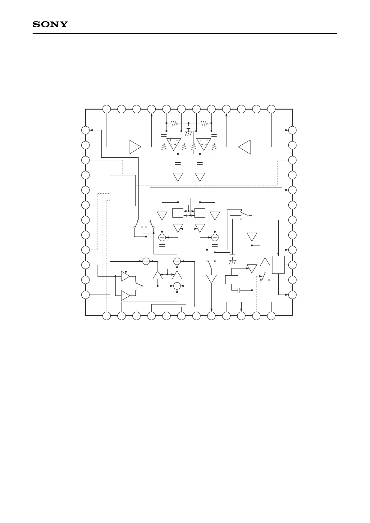
Block Diagram and Pin Configuration
ATF LEVEL
VCA
6dB
DOC
DET
BPF BPF
CONTROL
LOGIC
RP PB EN
C IN
VREG
AFM IN
VG
Y IN
V
CC
PCM RF OUT
AGC TC
AGC OUT
HCHG
RF IN A
2
3
4
5
6
7
8
9
10
12
1
MIX1 OUT
MT1
MULTI
GND 1CH
V RF OUT
GND PB
DOC IN
V
CC EF
RF OUT
DOC TC
RF IN B
DOC PULSE
13
14
15
16
17
18
19
20
21
22
23
24
MIX2 OUT
MT 2
RF SWP
GND 2CH
PCM SEL
ME LEVEL
GND REC
RP PB 1CH
ATF IN
RP PB 2CH
PCM IN
40
39
38
37
41
42
43
44
45
46
47
48
REC2 IN
MT Q
V
CC
2CH
REC2 OUT
PB IN 2P
PB IN 2N
PB IN 1N
PB IN 1P
REC1 OUT
V
CC
1CH
MT Fφ
REC1 IN
36
35
34
31
32
33
25
2627
28
29
30
CH2
REC AMP
CH1
REC AMP
CH1
HEAD AMP
46dB
9dB
CH2
HEAD AMP
46dB
9dB
VP2
SW
VP1
SW
P V P V
–6dB
MTFφ
MTQ
MT2
MT1
–6dB
CH2
CH1
Mute
Video
SW
6dB
DOC
DET
12dB
GCA
A B
RF SW
CH2 CH1
PCM
SW
MIX
AMP
6dB
RF
AGC
DET
11
ME
LEVEL
VCAVCA
ATF
SW
Medium range freq.
compensation
VCA VCA
Multi
Normal
Page 3
– 3 –
CXA1202Q-Z/CXA1202R
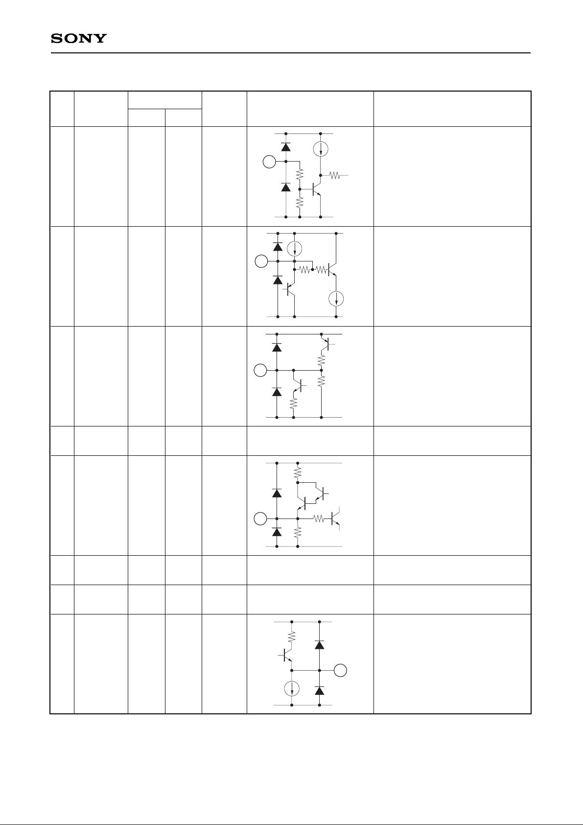
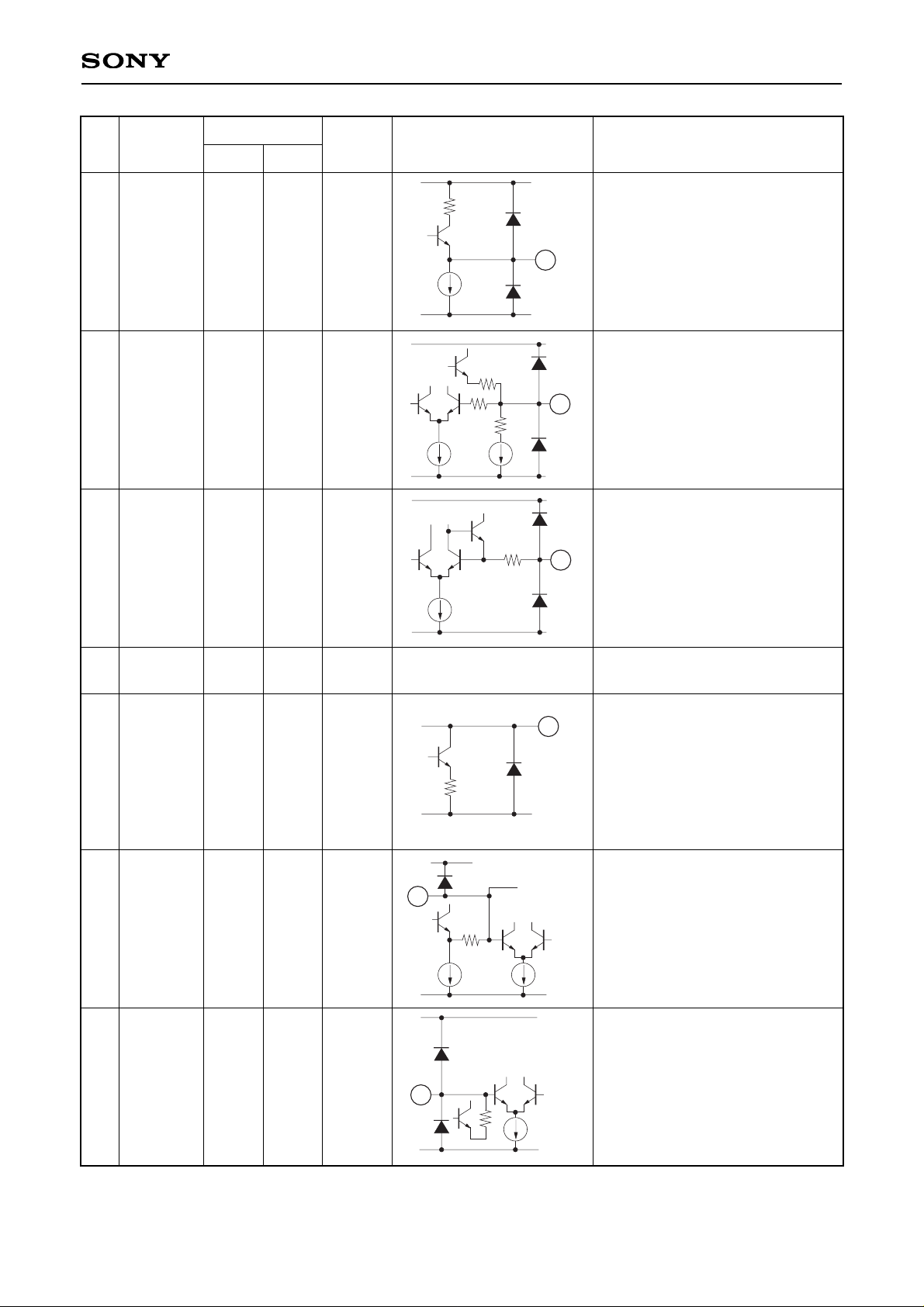
Pin Description
No.
1
2
3
4
5
6
7
8
RP PB EN
C IN
VREG
AFM IN
VG
Y IN
Vcc
PCM RF
OUT
(Open:
"L")
3.2V
4.2V
3.2V
2.5V
3.2V
5.0V
1.8V
—
134
mVp-p
—
80
mVp-p
—
250
mVp-p
—
50 to
500
mVp-p
40kΩ
20kΩ
—
20kΩ
—
20kΩ
—
Emitter
follower
(IE = 1mA)
Symbol
Equivalent circuit
Description
I/O
resistance
DC
AC
Voltage
1
V
CC
GND
40k
20k
VCC
GND
20k
2
100
VCC
GND
3
24k
35k
VCC
GND
2.5k
150
5
1mA
VCC
GND
8
440
Power-save recording at Low.
High: over 3V
Low: under 1V
Input pin for Chroma signal.
Output pin for VREG 4.2V.
Decoupling with capacitance.
Input pin for AFM signal.
Output pin for virtual GND.
Decoupling with capacitance.
Input pin for Y signal.
Supply pin for circuits other than
REC AMP and Head AMP.
Output pin for PB PCM signal.
Same as for Pin No. 2
Same as for Pin No. 2
—
Page 4
– 4 –
CXA1202Q-Z/CXA1202R
No.
9
10
11
12
13
14
15
AGC TC
AGC OUT
HCHG
RF IN A
DOC
PULSE
RF IN B
DOC TC
4.25V
(Load:
150kΩ
2.5V
—
(Open:
"L")
2.5V
H: 3.2V
L: 0V
2.5V
2.5V
—
100
mVp-p
—
100
mVp-p
—
100
mVp-p
—
—
Emitter
follower
(IE = 1mA)
50kΩ
—
Emitter
follower
(H: IE =
1mA)
20kΩ
—
Symbol
Equivalent circuit
Description
I/O
resistance
DC
AC
Voltage
VCC
500
200
GND
9
200
1mA
VCC
GND
200
10
17
VCC
GND
11
50k
VCC
GND
150
20k
5
12
VCC
GND
100
80k 3.5k
13
VCC
GND
90
8k
15
3.3k
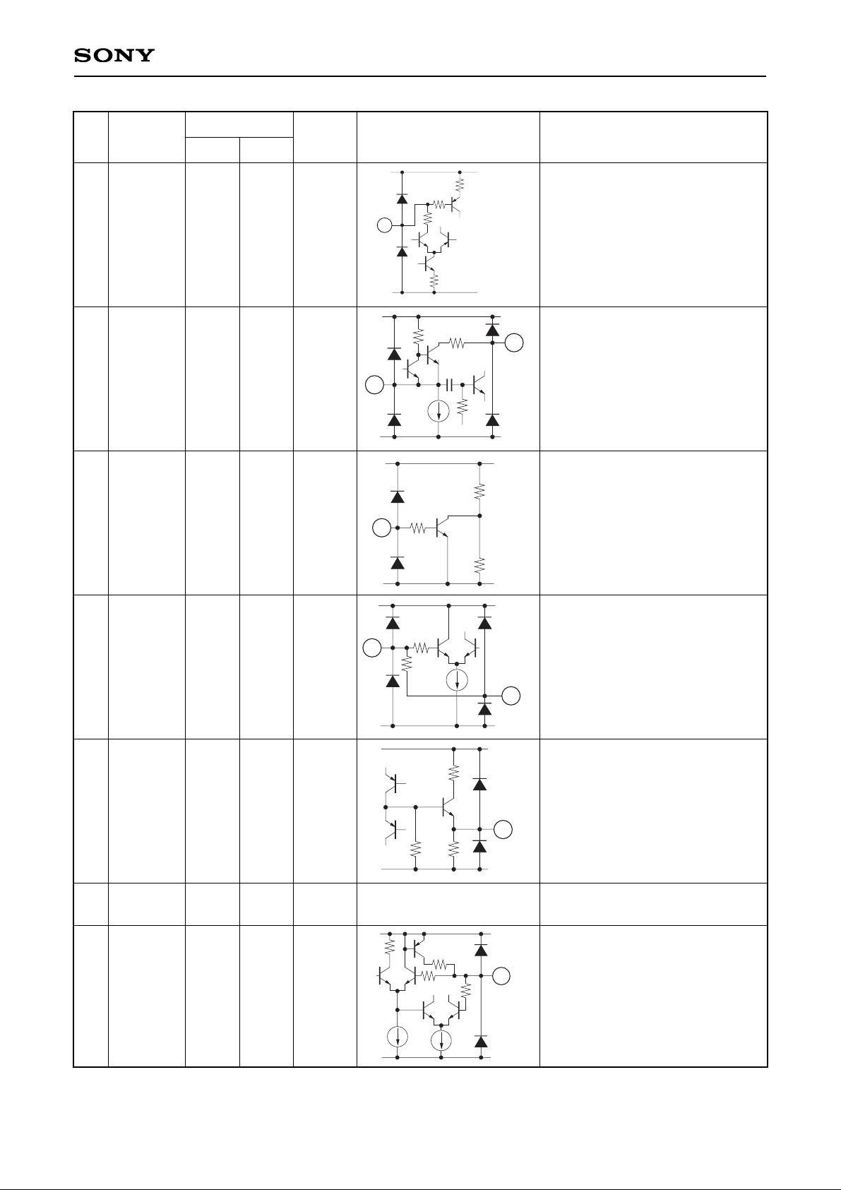
Pin to apply time constant of
envelope detection for RF AGC.
Optimum load resistance across
Vcc is 150kΩ.
AGC output pin for PB VIDEO
signal (Max. gain of AGC AMP is
about 7dB).
Control signal input pin for RF SW
switching:
High (over 3V): selects RF IN A
Low (under 0.3V):
selects RF IN B
Input pin for RF switch and 12dB
AMP.
Dropout detection signal output
pin; High upon dropout.
Input pin for RF switch and 12dB
AMP.
Pin to connect time constant of
dropout detection.
Same as for Pin No. 12
Page 5
– 5 –
CXA1202Q-Z/CXA1202R
No.
16
17
18
19
20
21
22
23
RF OUT
Vcc EF
DOC IN
GND PB
V RF OUT
GND 1CH
MULTI
MT1
2.5V
5.0V
2.5V
0V
1.8V
0V
—
(OPEN:
"L")
—
(2.5V
at
OPEN
of pin)
400
mVp-p
—
400
mVp-p
—
50 to
500
mVp-p
—
—
—
Emitter
follower
(IE =
500µA)
—
8kΩ
—
Emitter
follower
(IE =
500µA)
—
40kΩ
100kΩ
Symbol
Equivalent circuit
Description
I/O
resistance
DC
AC
Voltage
500µA
VCC
GND
200
16
VCC
GND
200
17
VCC
GND
150
8k
18
2.5V
VCC
GND
400
20
500µA
VCC
GND
25k
23
47k 53k
5
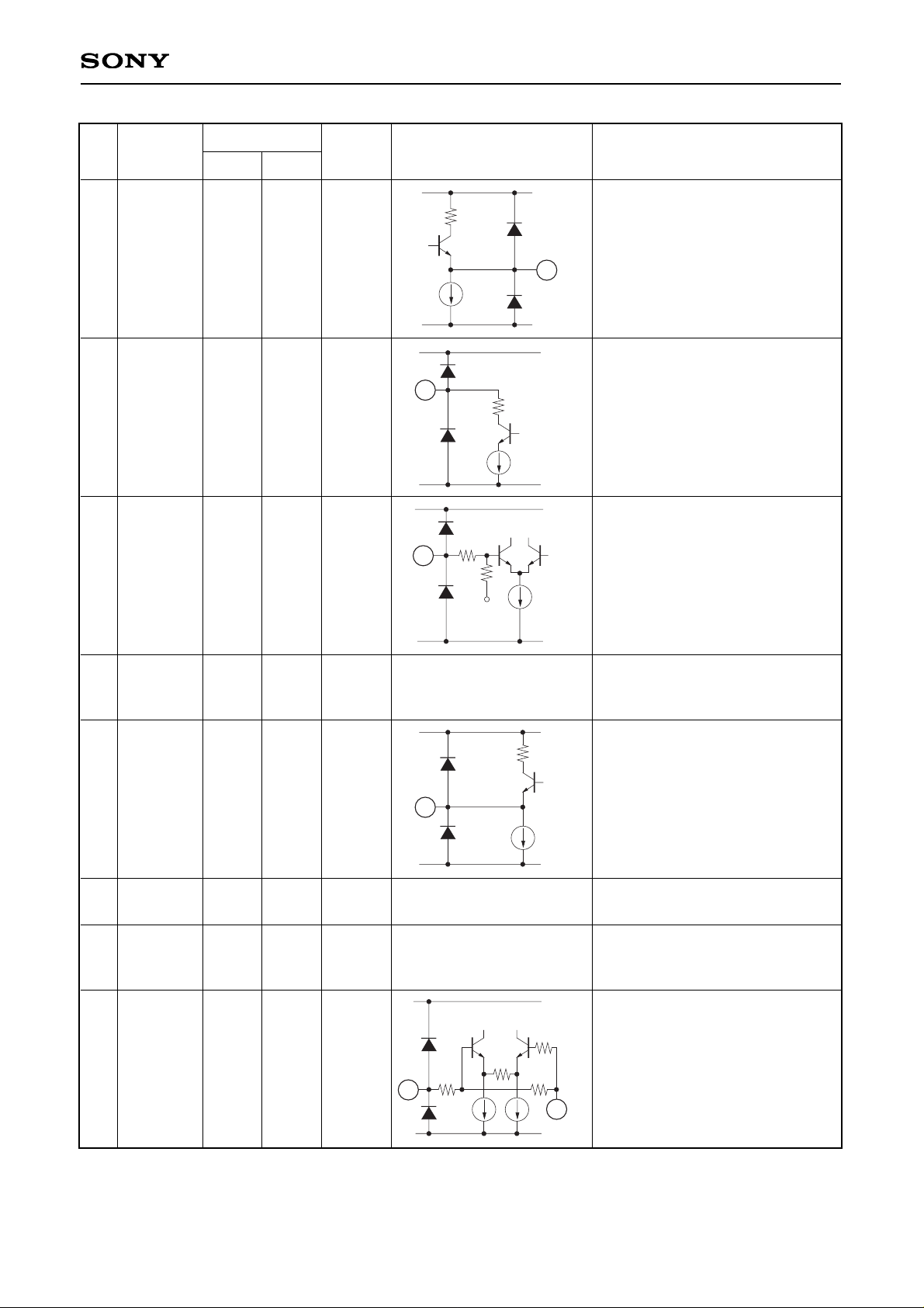
Output pin of signal selected by
HCHG from RF IN A and RF IN B.
Supply pin for emitter followers of
AGC OUT, DOC TC and RF OUT.
Input pin for dropout detection.
GND pin for medium range
frequency compensation circuit,
RF AGC and DOC DET.
Output pin for PB VIDEO signal.
GND pin for CH1 REC AMP and
CH1 Head AMP.
Multi-channel PCM REC mode at
High.
Boost level adjusting pin for CH1
medium range frequency
compensation circuit.
Variable between 0 and +12dB at
4.2 to 0.8V.
—
—
Same as for Pin No. 1
Page 6
– 6 –
CXA1202Q-Z/CXA1202R
No.
24
25
26
27
28
29
30
MIX1 OUT
REC1 IN
MT Fφ
Vcc 1CH
REC1 OUT
PB IN 1P
PB IN 1N
2.5V
1.8V
2.5V
5.0V
15mA
2.4V
2.4V
203
mVp-p
92µA
(Y signal)
—
—
13
mAp-p
90 to
900
µVp-p
—
Emitter
follower
(IE = 1mA)
~
–
0
—
—
Open
collector
1.3kΩ
1.3kΩ
Symbol
Equivalent circuit
Description
I/O
resistance
DC
AC
Voltage
1mA
VCC
GND
400
24
VCC
GND
100
200
100
25
VCC
GND
90
26
GND
20
28
VCC
GND
10k
29
VCC
GND
30
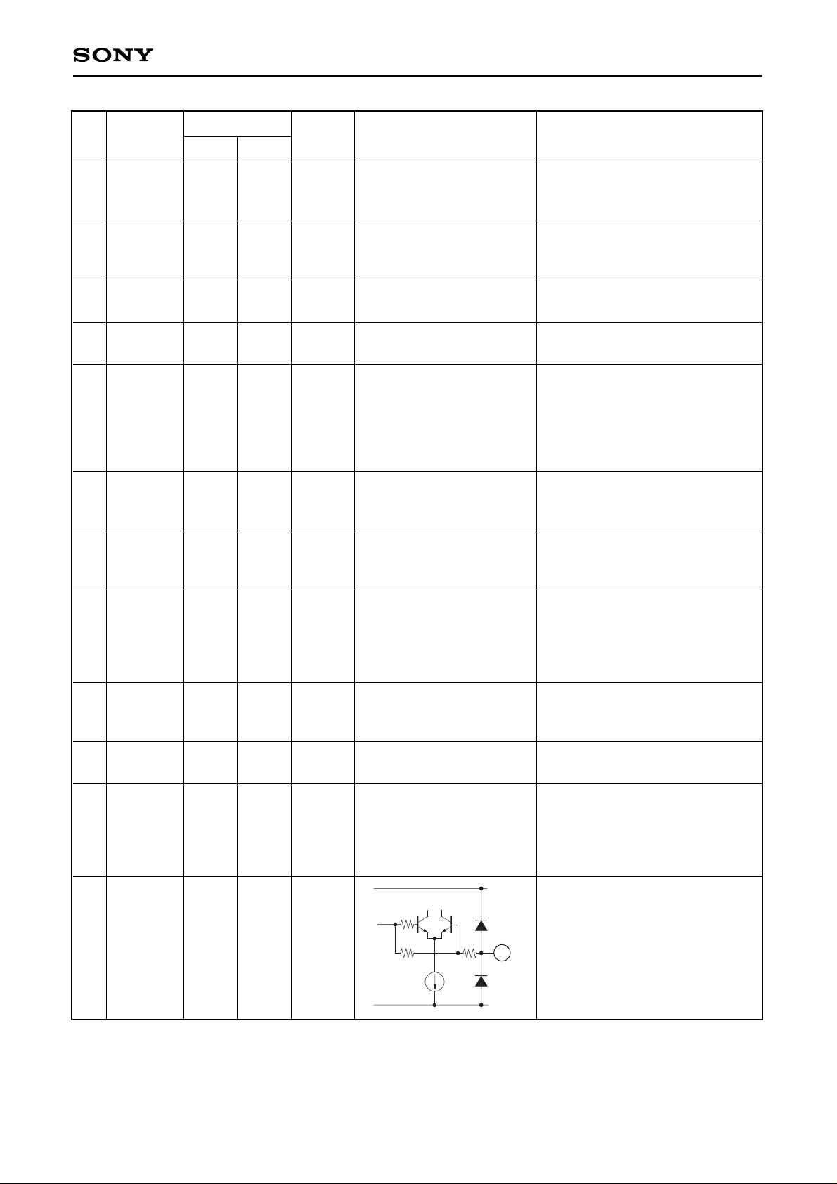
Mix circuit output pin for CH1.
CH1 REC AMP input pin.
Fφ adjusting pin for medium range
frequency compensation circuit;
Fφ is controlled through current
value by connecting resistance
between GNDs. Mutually affected
by MT Q. Do not connect
capacitance.
Power supply pin for CH1 REC
AMP and CH1 Head AMP.
CH1 REC AMP output pin.
CH1 head AMP positive phase
input pin (PB signal input pin).
CH1 Head AMP inverter phase
input pin (decoupling with
capacitance).
—
Page 7
– 7 –
CXA1202Q-Z/CXA1202R
No.
31
32
33
34
35
36
37
38
39
40
41
42
PB IN 2N
PB IN 2P
REC2 OUT
Vcc 2CH
MT Q
REC2 IN
MIX2 OUT
MT 2
RF SWP
GND 2CH
PCM SEL
ME LEVEL
2.4V
2.4V
15mA
5.0V
2.5V
1.8V
2.5V
—
(2.5V
at
OPEN
of pin)
—
(Open:
"L")
0V
—
(Open:
"L")
—
(2.1V
at
OPEN
of pin)
—
90 to
900
µVp-p
13
mAp-p
—
—
92µA
(Y signal)
203
mVp-p
—
—
—
—
—
1.3kΩ
1.3kΩ
—
—
~
–
0
Emitter
follower
(IE = 1mA)
100kΩ
40kΩ
—
40kΩ
100kΩ
Symbol
Equivalent circuit
Description
I/O
resistance
DC
AC
Voltage
VCC
GND
24k 76k
2.1V
18k
42
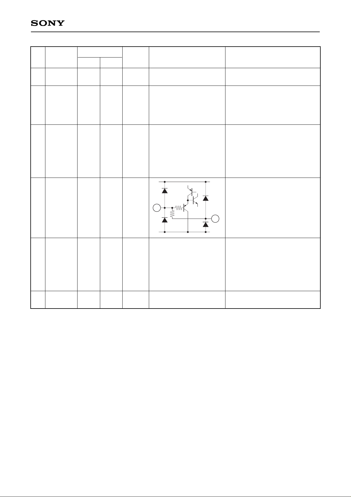
CH2 Head AMP Inverter phase
input pin (decoupling with
capacitance).
CH2 Head AMP positive phase
input pin (PB signal input pin).
CH2 REC AMP output pin.
Power supply pin for CH2 REC
AMP and CH2 Head AMP.
Q adjusting pin for medium range
frequency compensation circuit.
Controls Q through current value
by connecting resistance between
GNDs; Mutually effected by MT
Fφ. Do not connect capacitance.
CH2 REC AMP input pin.
Mix circuit output pin for CH2.
Boost level adjusting pin for CH2
medium range frequency
compensation circuit; variable
between 0 and +12dB at 4.2 to 0.8V.
RF switching pulse input pin for
CH switchover.
GND pin for CH2 REC AMP and
CH2 head AMP.
PCM AREA input pin;
High: PCM REC period
During High period after recording,
MUTE is applied to PB VIDEO
output.
Level of low range REC signals
(Chroma, AFM, ATF rec. with
VIDEO) can be boosted by 0 to
3dB by voltage (0 to 5V) applied
to this pin.
Same as for Pin No. 30
Same as for Pin No. 29
Same as for Pin No. 28
Same as for Pin No. 26
Same as for Pin No. 25
Same as for Pin No. 24
Same as for Pin No. 23
Same as for Pin No. 1
Same as for Pin No. 1
—
—
Page 8
– 8 –
CXA1202Q-Z/CXA1202R
No.
43
44
45
46
47
48
GND REC
ATF
LEVEL
RP PB
1CH
ATF IN
RP PB
2CH
PCM IN
0V
—
(2.1V
at
OPEN
of pin)
—
(Open:
"L")
2.5V
—
(Open:
"L")
3.2V
—
—
—
250
mVp-p
—
250
mVp-p
—
100kΩ
40kΩ
20kΩ
40kΩ
20kΩ
Symbol
Equivalent circuit
Description
I/O
resistance
DC
AC
Voltage
VCC
GND
20k
100
5
46
GND pin for VG, VREG, LOGIC
and mix circuit.
REC Ievel of ATF signal can be
boosted by 0 to 3dB by the voltage
(0 to 5V) applied to this pin.
In multi PCM mode, priority given
to 6dB AMP.
REC/PB switchover signal for CH1:
High: PB
Low: REC
However, when RP PB EN pin is
at Low:
High: power save REC
Low: REC
Input pin for ATF pilot signal.
REC/PB switchover signal for CH2:
High: PB
Low: REC
However, when RP PB EN pin is
at Low:
High: power save REC
Low: REC
Input pin for PCM signal.
—
Same as for Pin No. 42
Same as for Pin No. 1
Same as for Pin No. 1
Same as for Pin No. 2
Page 9
– 9 –
CXA1202Q-Z/CXA1202R
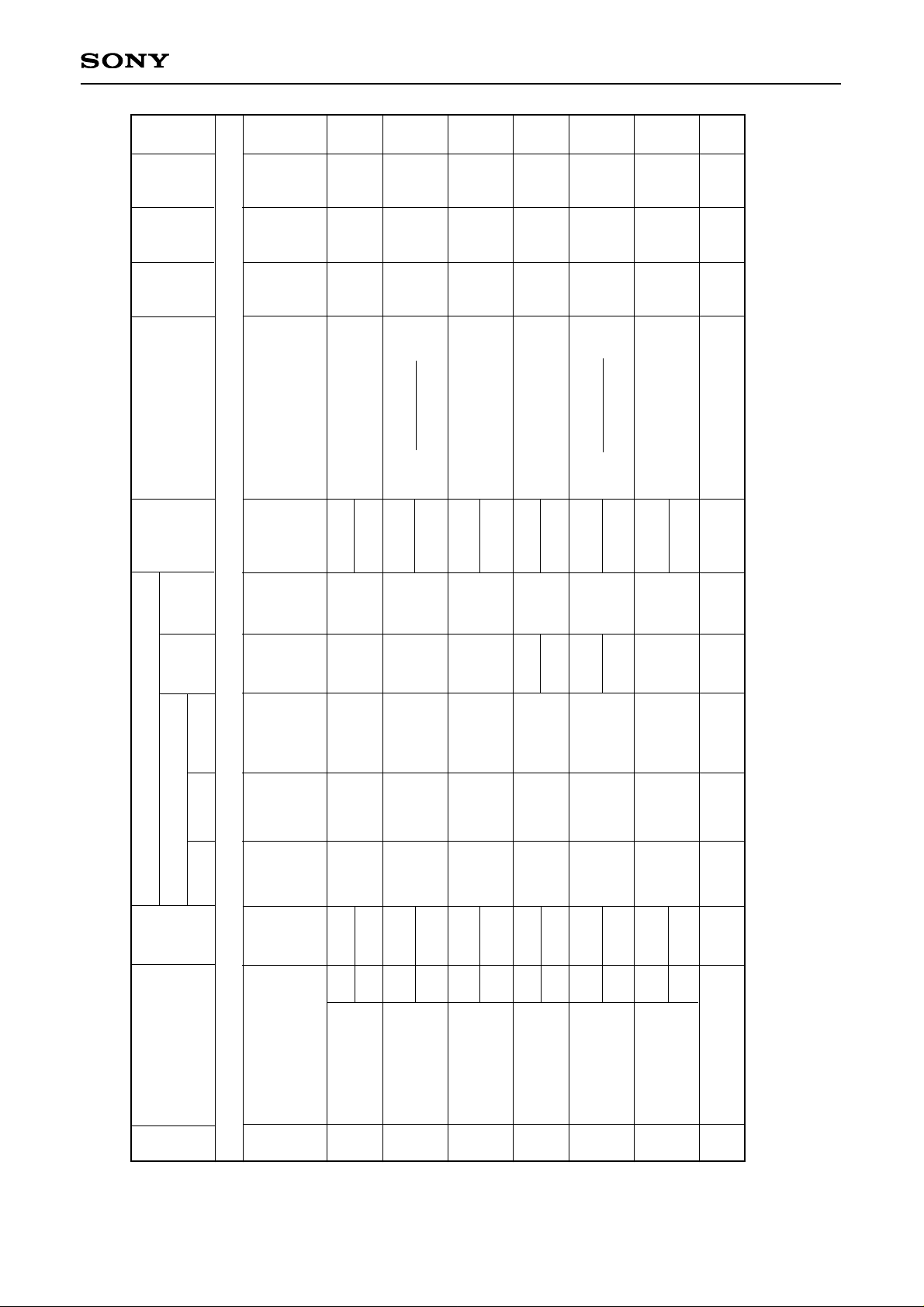
Electrical Characteristics
(Ta = 25°C, Vcc = 5V, See the Electrical Characteristics Test Circuit.)
No. Item
REC mode circuit
current
Mix AMP
Y gain
Mix AMP
Y frequency
response
Mix AMP
Y secondary
distortion factor
Mix AMP
PCM gain
Mix AMP
PCM frequency
response
Mix AMP
PCM secondary
distortion factor
Mix AMP
Chroma gain
In both CH REC, internal
consumption current
(excluding REC output
current)
10MHz Ievel
1MHz Ievel
10MHz Ievel
1MHz Ievel
At min. gain of 0V at ME
LEVEL pin
Symbol
Test method
Min.
Typ.
Max.
Unit
Test point,
Ammeter
name
Test conditions
Input condition
Input pin
Level
Frequency
Control
logic
∗
1
Other
SW ON
1
2
3
4
5
6
7
8
20.5
–2.6
–1.0
–2.8
–1.0
–12.7
27.5
–1.8
–0.2
–50
–1.8
–0.2
–50
–11.7
35.0
–1.0
–40
–0.8
–40
–10.7
mA
dB
dB
dB
dB
dB
dB
dB
CH1
CH2
CH1
CH2
CH1
CH2
CH1
CH2
CH1
CH2
CH1
CH2
IREC
GY1
GY2
VFY1
VFY2
DY1
DY2
GP1
GP2
VFP1
VFP2
DP1
DP2
GC1
6
6
6
48
48
48
2
1MHz
10MHz
1MHz
5MHz
1MHz
10MHz
1MHz
5MHz
750kHz
250
mVp-p
250
mVp-p
500
mVp-p
250
mVp-p
250
mVp-p
500
mVp-p
150
mVp-p
A
A
B
C
F
E
J
K
K
D
I
VCC
24
37
24
37
24
37
24
37
24
37
24
37
24
42, 44
∗1
See the Control Logic Truth Table for control logic conditions.
<Recording>
Page 10
– 10 –
CXA1202Q-Z/CXA1202R
(Ta = 25°C, Vcc = 5V, See the Electrical Characteristics Test Circuit.)
No. Item
Mix AMP
Low range freq.
(Chroma, AFM,
ATF rec. with VIDEO)
variable gain by ME
LEVEL pin
Mix AMP
Chroma secondary
distortion factor
Mix AMP
AFM gain
Mix AMP
AFM secondary
distortion factor
Mix AMP
ATF gain
(rec. with VIDEO)
Mix AMP
ATF gain
(rec, with PCM)
Mix AMP
ATF variable gain
by ATF LEVEL pin
Mix AMP
ATF rec. with PCM
variable gain by ME
LEVEL pin
Change in gain when ME
LEVEL pin is brought
from 0 to 5V
At max. gain of 5V at ME
LEVEL pin
At min. gain of 0V at ME
LEVEL pin
At max. gain of 5V at ME
LEVEL pin
At min. gain of 0V at both
ME LEVEL pin and ATF
LEVEL pin
At min. gain of 0V at both
ME LEVEL pin and ATF
LEVEL pin
Change in gain when
ATF LEVEL pin is
brought from 0 to 5V
Change in gain when ME
LEVEL pin is brought
from 0 to 5V
Symbol
Test method
Min.
Typ.
Max.
Unit
Test point,
Ammeter
name
Test conditions
Input condition
Input pin
Level
Frequency
Control
logic
∗
1
Other
SW ON
9
10
11
12
13
14
15
16
2.4
–11.2
–28.9
–28.9
2.4
2.3
3.4
–50
–10.1
–50
–27.6
–27.6
3.4
3.3
4.4
–40
–9.0
–40
–26.3
–26.3
4.4
4.3
dB
dB
dB
dB
dB
dB
dB
dB
∆GME
DCI
GAF1
DAF1
GATV
GATP
∆GATA
∆GATM
2
2
4
4
46
46
46
46
750kHz
750kHz
1.5MHz
1.5MHz
100kHz
100kHz
100kHz
100kHz
150
mVp-p
250
mVp-p
100
mVp-p
250
mVp-p
250
mVp-p
250
mVp-p
250
mVp-p
250
mVp-p
D
E
K
D
F
J
J
J
J
24
24
37
37
37
24
37
24
42
42
42
44
42
∗1
See the Control Logic Truth Table for control logic conditions.
Page 11

– 11 –
CXA1202Q-Z/CXA1202R
(Ta = 25°C, Vcc = 5V, See the Electrical Characteristics Test Circuit.)
No. Item
Mix AMP
ATF gain increment
at multi PCM
REC AMP
output bias
current
REC AMP
output bias
current
REC AMP
channel balance
REC AMP
frequency
response
REC AMP
secondary
distortion factor
Head AMP
VRF OUT gain
Head AMP
PCM RF OUT
gain
AGC OUT Ievel
Change in gain when
control logic is set to
multi PCM
DC current testing
Output level [V]
100 [Ω]
Difference in output level
between CH1 and CH2
10MHz Ievel
1MHz Ievel
Symbol
Test method
Min.
Typ.
Max.
Unit
Test point,
Ammeter
name
Test conditions
Input condition
Input pin
Level
Frequency
Control
logic
∗
1
Other
SW ON
17
18
19
20
21
22
23
24
25
4.9
13.4
12.0
–0.8
–3.2
52.2
52.2
70
5.9
15.7
13.2
0.0
–2.1
–49
54.5
54.5
95
6.9
18.0
14.4
0.8
–40
57.2
57.2
120
dB
mA
mA
p-p
dB
dB
dB
dB
dB
mV
p-p
∆GATMU
46
25
36
25
36
25
36
25
36
29
32
29
32
29
100kHz
1MHz
1MHz
10MHz
1MHz
5MHz
1MHz
1MHz
5MHz
250
mVp-p
200
mVp-p
200
mVp-p
200
mVp-p
300
mVp-p
200
µVp-p
200
µVp-p
200
µVp-p
J
G
A
F
F
B
E
H
I
I
H
H
24
I
REC1
IREC2
28
33
28
33
28
33
28
33
20
8
10
23
38
23
38
23
CH1
CH2
CH1
CH2
CH1
CH2
CH1
CH2
I
DR1
IDR2
IR1
IR2
∆VR21
∆VFR1
∆VFR2
DR1
DR2
GV1
GV2
GP1
GP2
VAGC
CH1
CH2
CH1
CH2
<Playback>
∗1
See the Control Logic Truth Table for control logic conditions.
Page 12

– 12 –
CXA1202Q-Z/CXA1202R
(Ta = 25°C, Vcc = 5V, See the Electrical Characteristics Test Circuit.)
No. Item
AGC control
characteristics "H"
AGC control
characteristics "L"
DC offset between
channels
CH1 – CH2
DC offset at MUTE,
CH1, CH2 – MUTE
RF SW gain
RF SW
frequency
response
Dropout detection,
ON level
Output level at
input 900µV
Output level at
input 200µV
Output level at
input 100µV
Output level at
input 200µV
DC voltage testing
At CH1 Low input –
at CH2 High input
At CH2 High input –
at CH1 Low input
Difference of DC voltage
at logic switchover
10MHz Ievel
300kHz Ievel
Pin 18 Ievel when DOC
PULSE pin becomes High
(0dB = 400mVp-p)
Symbol
Test method
Min.
Typ. Max.
Unit
Test point,
Ammeter
name
Test conditions
Input condition
Input pin
Level
Frequency
Control
logic
∗
1
Other
SW ON
26
27
28
29
30
31
32
–0.3
–0.8
–60
–60
11.1
–2.0
–16.5
0.5
–0.1
0
0
12.1
–0.4
–13.0
1.3
0.6
60
60
13.1
–10.5
dB
dB
mV
mV
dB
dB
dB
∆VAGCH
∆VAGCL
∆VDC12
∆VDCM
GRFA
GRFB
∆VFRFA
∆VFRFB
VD ON
29
29
29
32
29
32
12
14
12
14
12
5MHz
5MHz
1MHz
1MHz
300kHz
10MHz
300kHz
900
µVp-p
200
µVp-p
100
µVp-p
200
µVp-p
100
µVp-p
900
µVp-p
100
µVp-p
100
mVp-p
100
mVp-p
H
H
H
I
H → J
I → J
H
I
J
K
H
10
10
10
10
16
16
18
23
23
23
38
23
38
11
11
11
∗
1
See the Control Logic Truth Table for control logic conditions.
A input
B input
A input
B input
See the following
figure
∗2
Page 13

– 13 –
CXA1202Q-Z/CXA1202R
(Ta = 25°C, Vcc = 5V, See the Electrical Characteristics Test Circuit.)
No. Item
Dropout detection,
OFF Ievel
Dropout pulse,
Low level
Dropout pulse,
High level
PB mode circuit
current
VG pin DC voltage
VREG pin DC voltage
Pin 18 Ievel when DOC
PULSE pin becomes Low
(0dB = 400mVp-p)
DC voltage testing
DC voltage testing
Current consumption
with both CH
S in PB
Symbol
Test method
Min.
Typ.
Max.
Unit
Test point,
Ammeter
name
Test conditions
Input condition
Input pin
Level
Frequency
Control
logic
∗
1
Other
SW ON
33
34
35
36
37
38
–9.5
3.1
30.0
2.41
4.08
–7.0
0.0
3.2
40.0
2.51
4.23
–5.0
0.1
3.4
50.5
2.61
4.38
dB
V
V
mA
V
V
VD OFF
VPDL
VPDH
IPB
VG
VREG
12
12
5MHz
100
mVp-p
I
H
H
H
H
A
18
13
13
I
VCC
5
3
11
11
11
42.44
<Standard voltage supply in IC>
∗
1
See the Control Logic Truth Table for control logic conditions.
∗2
Signal description of dropout detection.
see the figure
below
∗
2
OFF level
ON level
ON, OFF level testing at Pin 18
100µs
100mVp-p
5MHz
3.2V
0V
Pin 12 input signal
Pin 13 DOC PULSE
Page 14
– 14 –
CXA1202Q-Z/CXA1202R
Control Logic Truth Table
Input
condition
and
operation
Control
Iogic
condition
Control Iogic input condition
Operation of each section under respective input condition
Recording
Playback
(Pin 1) RP PB EN
(Pin 45) RP PB 1CH
(Pin 47) RP PB 2CH
(Pin 39) RF SWP
(Pin 22) MULTl
(Pin 41) PCM SEL
(Pin 24) MIX1 OUT
(Pin 37) MIX2 OUT
(Pin 28) REC1 OUT
(Pin 33) REC2 OUT
CH1 HEAD AMP
CH2 HEAD AMP
medium range freq.
compensation circuit,
DOC DET, RF SW
(Pin 8) PCM RF OUT
(Pin 10) AGC OUT
(Pin 20) V RF OUT
Operation Mode
A
B
C
D
E
F
G
H
I
J
K
L
M
H L L — L L
L L L — L L
L H L — L L
L L H — L L
H L L H L H
H L L L L H
H L L — H —
H H H H — L
H H H L — L
H L H L L H
H H L H L H
H L H L H H
H H L H H H
V V V V
V V V V
V V X V
V V V X
V P V P
P V P V
MP MP MP MP
X X X X
X X X X
P V P X
V P X P
MP MP MP X
MP MP X MP
X X X X X X
X X X X X X
X X X X X X
X X X X X X
X X X X X X
X X X X X X
X X X X X X
O O O CH2 CH1 CH1
O O O CH1 CH2 CH2
X O O O MUTE MUTE
(No
signal)
O X O O MUTE MUTE
(No
signal)
X O O O MUTE MUTE
(No
signal)
O X O O MUTE MUTE
(No
signal)
VIDEO REC
Power save
VIDEO REC
VIDEO
• PCM
REC
MULTI PCM REC
PB
VIDEO
• PCM
PCM after recording
MULTI • PCM
PCM after recording
REC
PB
PCM
after
recording
Page 15

– 15 –
CXA1202Q-Z/CXA1202R
1. Description of input condition
"High" … Control logic input, over 3V.
"Low" .… Control logic input, under 1V.
"—" …… Independent of High, Low.
2. Description of operation mode
O ……… Operating
X ……… Not operating
• In recording mode
V ......... VIDEO signal is output.
P ......... PCM signal is output.
MP....... ATF signal that passed through fixed 6-dB AMP in mix circuit is output, mixed with PCM signal.
• In playback mode
CH1 ...... CH1 signal is output.
CH2 ...... CH2 signal is output.
MUTE ... MUTE is applied to PB VIDEO signal in PCM after recording; at the same time, RF AGC gain is held.
Page 16

– 16 –
CXA1202Q-Z/CXA1202R
Electrical Characteristics Test Circuit
RP PB EN
CIN
AFM IN
VG
Y IN
PCM RF
OUT
AGC
OUT
HCHG
RF IN A
MIX1
OUT
MT1
V RF
OUT
RF
OUT
DOC
PULSE
MIX2
OUT
MT 2
RF SWP
PCM SEL
ME LEVEL
RP PB 1CH
ATF IN
RP PB 2CH
PCM IN
REC2 IN
MT Q
PB IN 1P
MT Fφ
REC1 IN
0.047µ
0.047µ
50 50
0.1µ
50
0.01µ
0.1µ
1k
0.1µ
5.8k
0.047µ
150k 50
0.047µ
3V0.3V
0.1µ
22k
MULTI
0.01µ
0.1µ 5.8k
0.01µ
0.1µ 5.8k
47k
50
0.047µ
RF IN B
100k
220p
150k
2.2k
0.1µ
50
51k
0.33µ0.22µ0.22µ0.33µ
3.3
33p
5.6µ
PB IN 2P
3.3
33p
5.6µ
2.2k
0.1µ
50
8.2k
22k
2.2k0.1µ2.2k
SW38
SW23
ATF LEVEL
0.047µ
0.01µ
50
50
0.1µ 22µVCC 5V
IVCC
IREC2 IREC1
100100
∗
∗
∗
∗
∗
∗
∗
Signal output pin (Test)
Control logic pin
Signal input pin (Input level control point)
Signal source impedance: 50Ω
Resistance accuracy: 1%
Control point of input manner and input
level of signal to head AMP:
input by attenuating 50Ω signal
source to 1/50 as shown below.
Input level is controlled at 1/50.
PB IN 1P
PB IN 2P
50Ω
49Ω
1Ω
Signal source
VCA
6dB
DOC
DET
BPF BPF
CONTROL
LOGIC
2
3
4
5
6
7
8
9
10
12
1
13
14
15
16
17
18
19
20
21
22
23
24
40
39
38
37
41
42
43
44
45
46
47
48
36
35
34
31
32
33
25
2627
28
29
30
CH2
REC AMP
CH1
REC AMP
CH1
HEAD AMP
46dB
9dB
CH2
HEAD AMP
46dB
9dB
VP2
SW
VP1
SW
P V P V
–6dB
MTFφ
MTQ
MT2
MT1
–6dB
CH2
CH1
Mute
Video
SW
6dB
DOC
DET
12dB
GCA
A B
RF SW
CH2 CH1
PCM
SW
MIX
AMP
6dB
RF
AGC
DET
11
ME
LEVEL
VCAVCA
ATF
SW
VCA VCA
Multi
Normal
5V
SW42
SW44
0.1µ 10µ 25k
Medium range freq.
compensation
Page 17
– 17 –
CXA1202Q-Z/CXA1202R
Description of Operations
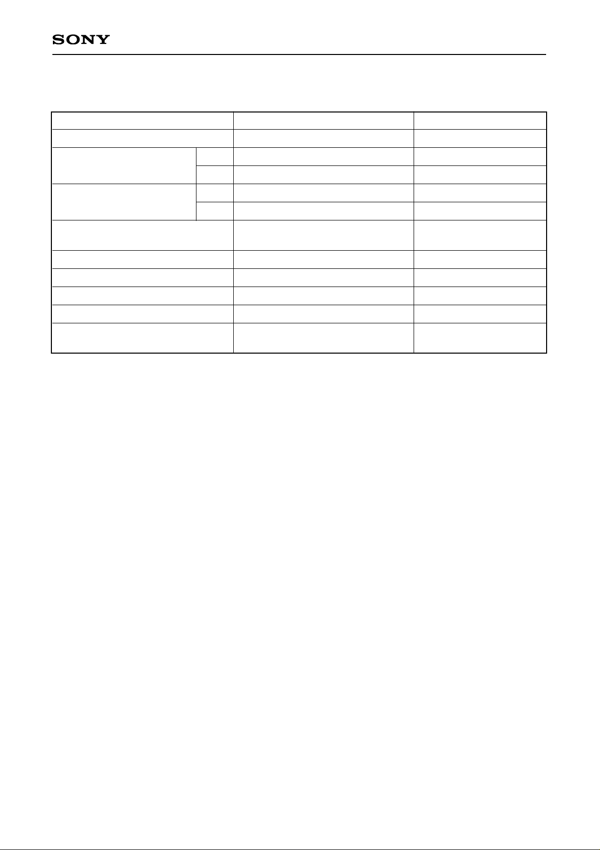
The functional blocks, voltage supply and GND pins of CXA1202Q-Z and CXA1202R are configured as follows:
Block name
Mix AMP + SW section
REC AMP section
Head AMP section
Medium range frq. compensation
circuit + SW section
RF AGC section
RF SW section
Dropout detecting section
Control logic section
Standard voltage supply section in IC
(VREG, VG)
7
27
34
27
34
7
7, 17 (Output emitter follower section)
7, 17 (Output emitter follower section)
7, 17 (Peak hold section)
7
7
43
21
40
21
40
19
19
19
19
43
43
Voltage supply pin GND pin
CH1
CH2
CH1
CH2
Individual blocks are described in the following paragraphs.
[Mix AMP + SW]
Here, each of Y, Chroma, AFM, ATF and PCM signals is input at a prescribed input level so that they are
mixed together internally to achieve an appropriate current value at the head, and output to MIX1 OUT pin
(CH1 signal) and MIX2 OUT (CH2 signal) at a correct timing.
Control is possible at ATF LEVEL pin (0 to 3dB at 0 to 5V, OPEN not allowed) when only the ATF recording
level is to be increased as required, and at ME LEVEL pin (0 to 3dB at 0 to 5V, OPEN not allowed) when only
the low range signal (Chroma + AFM + ATF) recording level is to be increased.
In MULTI PCM mode, the ATF recording level is boosted by 6dB.
In SW, the signal is output to MIX1 OUT and MIX2 OUT pins under control of the control logic section.
[REC AMP]
Mix AMP + SW output is input after it is converted into a suitable current by an external resistor, to drive the
head. Adjustment of the external resistor makes it possible to set a gain and DC bias current to match that of
the head.
Feedback dumping is applied to inhibit head resonance (refer to the Application Circuit), and take care that
capacitance coupling will not occur across the input and output.
Control signals of RP PB EN, RP PB 1CH and RP PB 2CH permit power saving in the channels while
recording (refer to the Control Logic Truth Table). Power saving of about 85mW is possible through a single
channel.
Page 18

– 18 –
CXA1202Q-Z/CXA1202R
[Head AMP]
The playback signal from the head is amplified with low noise and high gain. For example, the equivalent input
noise level at 1MHz is 662pVrms/ √Hz.
∗1
In PB, the total input capacitance∗2will be about 75pF. To inhibit resonance between this capacitance and the
head inductance, a feedback dumping is incorporated.
Connect a bypass capacitor for PB IN 1N and PB IN 2N pins between these pins and the rotary transformer
Vcc. So far as this capacitor is over 0.2µF, the low-Ievel frequency response does not deteriorate. Beside the
0.1µF good frequency response capacitor connected to pin VREG, by adding a capacitor of over 10µF,
degradation of noise level at low range can be prevented.
Take care not to allow capacitance coupling between PB output and Head AMP input.
∗1
and ∗2See the next page.
[Medium range frequency compensation circuit + SW]
This corrects the frequency response of the PB signal. It is possible to set to and Q magnitude by means of the
external resistance value of MT Fφ and MTQ pins (refer to the Fφ graph). The amount of boost may be
adjusted through the external volumes of MT1 and MT2 pins (refer to the graph showing the effect of standard
response MT2 pin voltage on the amount of boost).
By controlling the control logic section, SW is changed over with the timing of RF SW (switching pulse), to
output PCM RF signals and VIDEO RF signals. Mute is applicable to VIDEO RF signals during PCM after
recording within the PCM recording area period.
[RF AGC]
The played back VIDEO RF signal are output here to achieve a constant level of 100mVp-p. The time constant
for AGC is set by means of the resistance and capacitance external to AGC TC pin.
At the input section of the detector a HPF with a cutoff frequency of about 1MHz is incorporated. This is to
permit detection within the Y signal band.
In PCM after recording, MUTE applies during the PCM recording area period to keep the gain on an
unchanged level.
[RF SW]
Signals input to RF IN A and RF IN B pins are selected by means of HCHG control signals and output via the
12-dB amplifier to RF OUT pin. This switch is utilized for SP/LP head changeover when a 4-head system is
employed.
[Dropout detection]
Dropout is detected here from RF signals of played-back VIDEO and dropout pulse is output. The time
constant is set by means of the external resistance and capacitance external to DOC TC pin.
The detection level is set in the interior with 400mVp-p input as standard to obtain optimum level.
Use an external coupling capacitance value of input of 47pF to achieve HPF function.
[Control Logic]
The IC is controlled from this section as it will save power when circuit blocks are not in use. Therefore, power
saving is automatically executed while all the power supplies are switched on. Many SWs are also available to
switch inputs or outputs with complicated timing. Internal logic circuits to control them are provided.
It is possible to achieve all possible combinations of inputs/outputs necessary for the basic operations by
means of the 13 modes shown in the Control Logic Truth Table.
L is set when the control logic pin is open.
[Standard voltage supplies in the IC]
VREG 4.2V and VG 2.5V are provided as the standard voltage supplies in the IC.
Page 19
– 19 –
CXA1202Q-Z/CXA1202R
∗
1
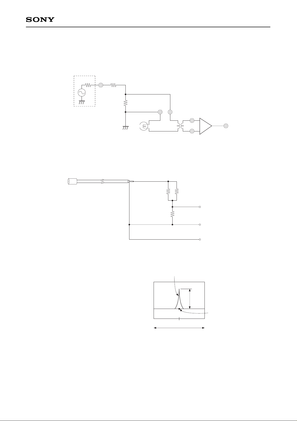
(Reference) Test Method of Head AMP C/N
(1) input signal
Level –42.0dBm [signal source: 50Ω]
(generates a voltage of 100µVp-p at both ends of 1Ω).
(2) Signal injection circuit
Fig. 1
The signal is input from A and B in Fig. 1. The equipment used for the input is shown in Fig. 2.
Notes) 1. A chip resistance is used for 1Ω (ordinary carbon resistance produces inductance.)
2. 49Ω is composed of 51Ω/1200Ω.
Fig. 2
50Ω 49Ω
1Ω
B A
CXA1202Q-Z
CXA1202R
head AMP
Head inductance
1.55µH
Winding ratio
3:5
Signal source
1Ω
51Ω 1200Ω
A
B
BNC
To drum GND
(3) SPECTRUM ANALYZER setting conditions:
RBW: 10kHz
VBW: 1Hz
Sweep time: 500s
Span: 500kHz
(4) Keep the medium range frequency compensation circuit flat. (Voltage of Pins MT1 and MT2 is made
equal to that of Pin VREG)
(5) Observe the output at Pin 20 V RF OUT.
∗2
The total input capacitance includes all capacitances of REC AMP, rotary transformer, shielding wire, etc.,
in addition to the input capacitance of the Head AMP alone (47pF).
During signal
During shortcircuit between A – B
C/N
5MHz
Span 500kHz
Page 20
– 20 –
CXA1202Q-Z/CXA1202R
ATF LEVEL
RP PB EN
C IN
VREG
AFM IN
VG
Y IN
V
CC
PCM RF
OUT
AGC
TC
AGC
OUT
HCHG
RF IN A
MIX1 OUT
MT1
MULTI
GND 1CH
V RF OUT
GND PB
DOC IN
V
CC EF
RF OUT
DOC TC
RF IN B
DOC
PULSE
MIX2 OUT
MT 2
RF SWP
GND 2CH
PCM SEL
ME LEVEL
GND REC
RP PB 1CH
ATF IN
RP PB 2CH
PCM IN
REC2 IN
MT Q
V
CC 2CH
REC2
OUT
PB IN 2P
PB IN 2N
PB IN 1N
PB IN 1P
REC1
OUT
V
CC
1CH
MT Fφ
REC1 IN
0.047µ
470k 220k
1000p
0.1µ 0.1µ
0.047µ
0.1µ
10µ
0.047µ
4.7k
3.9k
15k5.6k100k
0.01µ
0.022µ
∗ ∗
10k
DTC144
DTC
144
150k
56k
220p
1000p
DTA144
DTA144
DTA144
100k
∗
0.1µ0.1µ0.1µ0.1µ
27k
0.1µ
0.01µ 22k22k
0.1µ
0.01µ 22k22k
10k
10k
0.1µ
2200
10k
AMP
AFM
Trap
ATF
Trap
LPF
DOC PULSE
47p
AFM
Trap
ATF
Trap
C
Trap
S.L.
AFM
Trap
PF
EQ
Half
Trap
CXA1201M
CXA1200Q
PB C RF IN
DOP
PB Y RF
REC C
RF OUT
REC Y RF
VIDEO BLOCK
5V/0V
JOG : High
Normal : Low
JOG : High
Normal : Low
LPF
LPF
24
2
REC Pilot OUT
PB Pilot IN
EQ
BPF
VCO OUT
PBIN2
REC RF
7
8
44
ATF BLOCK
AFM BLOCK
CXA1204Q
CX20137
CH2 HEAD CH1 HEAD
22k
V
CC
0.01µ
47k
22k
To servo
To PCM
REC PCM
PB PCM
after recording area
To PCM
RF SWP
PCM area
To system
contoller
ME/MP
ATF LEVEL
MULTI
To system
contoller
GND
REG 5V
0.1µ
10µ
22µ
0.1µ
2200
22k
0.01µ
47k
22k
2
3
5
17
VCA
6dB
DOC
DET
BPF BPF
CONTROL
LOGIC
2
3
4
5
6
7
8
9
10
12
1
13
14
15
16
17
18
19
20
21
22
23
24
40
39
38
37
41
42
43
44
45
46
47
48
36
35
34
31
32
33
25
2627
28
29
30
CH2
REC AMP
CH1
REC AMP
CH1
HEAD AMP
46dB
9dB
CH2
HEAD AMP
46dB
9dB
VP2
SW
VP1
SW
P V P V
–6dB
MTFφ
MTQ
MT2
MT1
–6dB
CH2
CH1
Mute
Video
SW
6dB
DOC
DET
12dB
GCA
A B
RF SW
CH2 CH1
PCM
SW
MIX
AMP
6dB
RF
AGC
DET
11
ME
LEVEL
VCAVCA
ATF
SW
VCA VCA
Multi
Normal
0.047µ
Medium range freq.
compensation
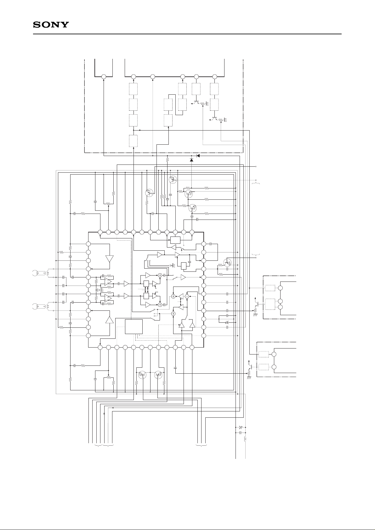
27k
59
60
Application Circuit
Application circuits shown are typical examples illustrating the operation of the
devices. Sony cannot assume responsibility for any problems arising out of the use of
these circuits or for any infringement of third party patent and other right due to same.
∗
Countermeasure for drop out pulse in EE or editing mode.
On a Virgin tape, drop out pulse shows with EE or editing mode in the absence of
playback output. In such case CXA1201M holds AGC gain. This may cause image
disturbance at the beginning of either recording or editing from EE mode.
To prevent this inconvenience, a 0V signal in recording and 5V in playback,
synchronized with the REC/PB signal of CXA1201M is entered. At 0V, the voltage of Pin
18 rises as if the input level for drop out detection had increased.
This prevents the drop out pulse even if there is no signal.
∗∗
Drop out countermeasures for virgin tape in playback.
During playback of virgin tape, as drop out pulse is generated, drop out compensation is
activated for long periods to deal with noise. V sync is disturbed and the picture loses its
clarity.
To prevent that, drop out pulse is passed through HPF and after continuation for a
certain period the pulse disappears.
Page 21
– 21 –
CXA1202Q-Z/CXA1202R
Precautions
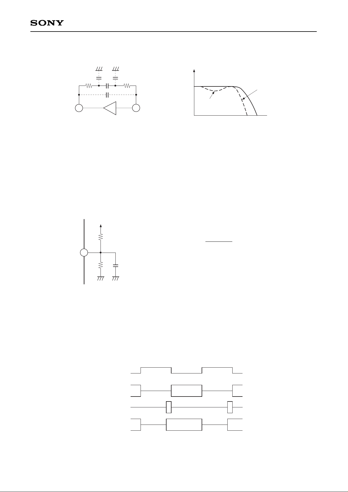
1. Do not connect parasite capacitance to REC AMP dumping.
Time constant: t = C × (R1//R2)
C: over 150pF
R1, R2: 5 × = 1.2 to 2.0V
Oscillations may occur unless this condition is satisfied.
R2
R1 + R2
15
C
R2
R1
V
CC
DOC TC
Frequency
Effect of C1
Effect of C2
Recording current
C1 C1
C2
25
28
REC AMP
2. Do not bring Head AMP input near PB output.
Normally, there is a gain of 67dB between Head Amp input (Pins 29, 30) and RFOUT (Pin 16). During no
signal, the gain is 74dB (as AGC reaches maximum gain). Bringing those closer on the pattern may cause
oscillations in the vicinity of 6 to 7MHz.
3. Use 150kΩ for RF AGC time constant, Resistance
Because a change in this R causes a change in the AGC output level, change the time constant using the
value of capacitance.
4. Watch the time constant of dropout detection.
5. Take AFM PB output from V RF OUT (Pin 20)
Passing AFM signal through RF AGC causes AGC to reach maximum gain when playing back a virgin tape.
As a result MUTE may not apply to AFM IC (CX20137, CX20037).
6. Adjust tape path by mixing V RE OUT signal and PCM RF OUT signal. In the absence of a signal before
switching, observe the envelope comprising the combination of the VIDEO area and the PCM area by
mixing outputs from V RF OUT (Pin 20) and PCM RF OUT (Pin 8).
RF SWP
V RF OUT
PCM RF OUT
After mixing
Page 22
– 22 –
CXA1202Q-Z/CXA1202R
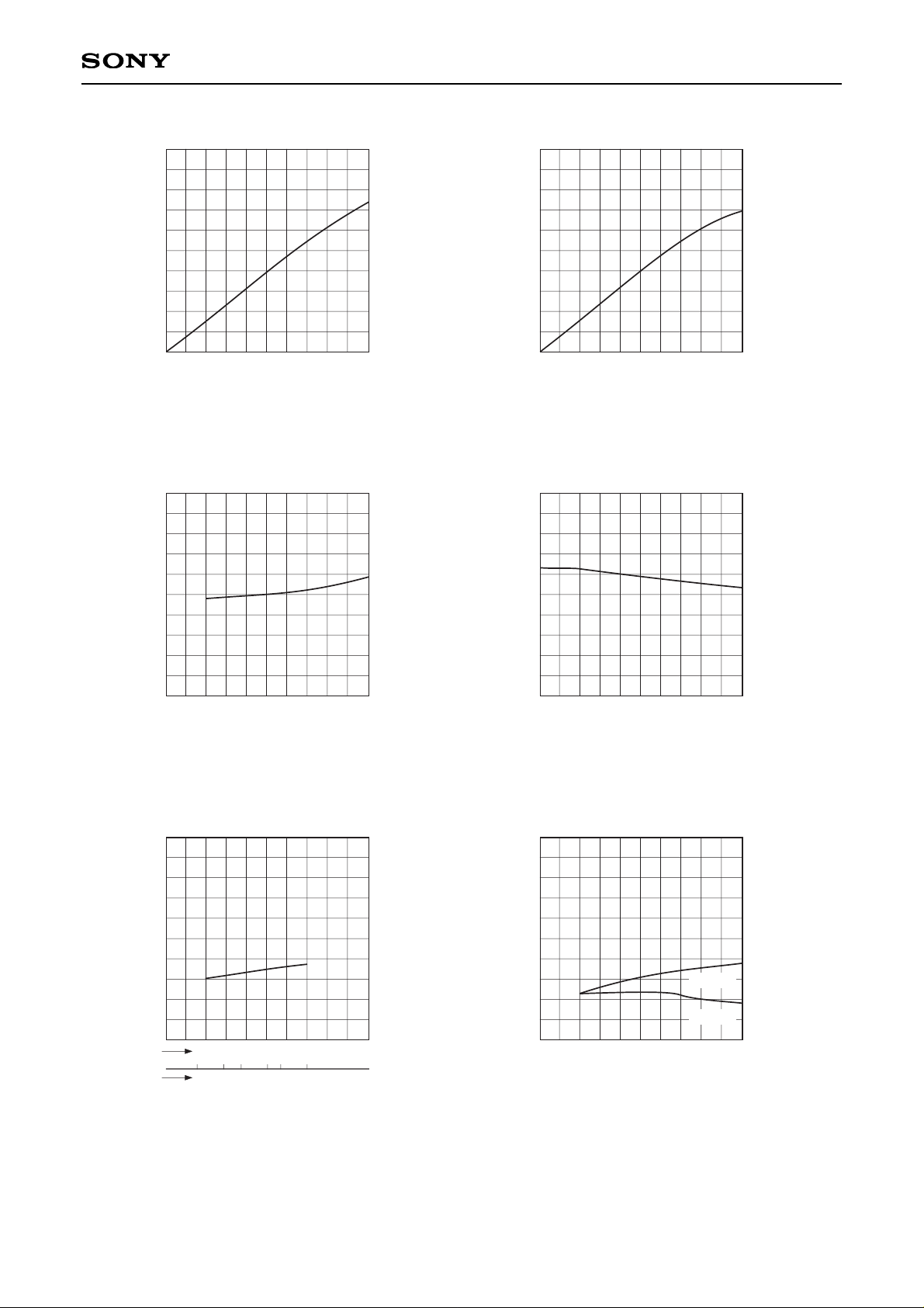
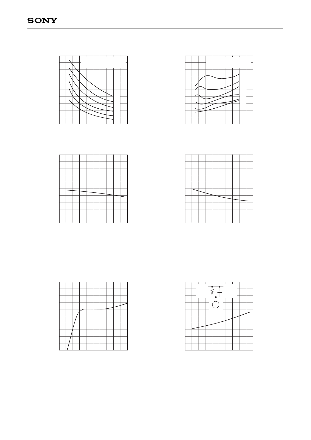
Mix AMP Chroma gain vs. ME LEVEL pin voltage
5
4
3
2
1
ME LEVEL pin voltage [V]
Gain [dB]
0 1 2 3 4 5
Conditions: Input: Pin 2, 126mVp-p, 750kHz
Output: Pin 24
Logic A
Mix AMP ATF gain vs. ATF LEVEL pin voltage
5
4
3
2
1
ATF LEVEL pin voltage [V]
Gain [dB]
0 1 2 3 4 5
Conditions: Input: Pin 46, 250mVp-p, 100kHz
Output: Pin 24
Logic A
Mix AMP Y output secondary distortion
factor vs. Frequency
–40
f – Frequency [MHz]
Secondary distortion factor [dB]
2 4 6 8 10
Conditions: Input: Pin 6, 250mVp-p
Output: Pin 37
Logic A
–50
–60
–40
–50
–60
Input level
Secondary distortion factor [dB]
–16
Conditions: Input: At resistance (2.2kΩ) with Pin 25, 5MHz
Output: Pin 28, load resistance: 100Ω
Logic A
–14–12–10 –8 –6 –4
Output current
8 10 1315 20
6
0 [dBm]
[mAp-p]
REC AMP distortion factor vs. Frequency
–40
–50
–60
f – Frequency [MHz]
Distortion factoc [dB]
2 4 6 8 10
Conditions: Input: At resistance (2.2kΩ) with Pin 25, 200mVp-p
Output: Pin 28, load resistance: 100Ω
Logic A
REC AMP frequency response
f – Frequency [MHz]
Relative gain [dB]
0 4 8 12 16 20
Conditions: Input: At resistance (2.2kΩ) with Pin 25, 200mVp-p
Output: Pin 28, load resistance: 100Ω
Logic A
–5
5
0
–10
2 6 10 14 18
Second
Third
REC AMP secondary distortion factor
vs. input level, output current
Page 23
– 23 –
CXA1202Q-Z/CXA1202R
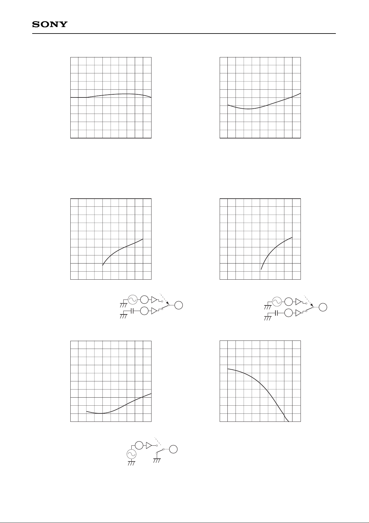
Head AMP output level vs. Frequency
5
–5
0
f – Frequency [MHz]
Change in output level [dB]
2 4 6 8 10
Conditions: Input: 25µm-wide head for NTSC, 100mVp-p at head tip
Output: Pin 20
Logic H, medium range freq. conpensation circuit boost: 0
V RF OUT secondary distortion factor vs.
Input level
–40
–50
–60
Input level [dB]
Secondary distortion factor [dB]
–4 0 4 8 12
Conditions: Input: Pin 29, 0dB = 200mVp-p, 5MHz
Output: Pin 20
Logic H
f – Frequency [MHz]
–30
Crosstalk [dB]
–40
–50
CH1 → CH2 crosstalk at PCM RF OUT vs.
Frequency
2 4 6 8
Conditions: Input: Pin 29, 200µVp-p
Output: Pin 8
Logic H
29
32
2
Crosstalk
CH1 → CH2 crosstalk at RF OUT vs. Frequency
–30
f – Frequency [MHz]
Crosstalk [dB]
2 4 6 8
Conditions: Input: Pin 29, 200µVp-p
Output: Pin 20
Logic I
–40
–50
29
32
Crosstalk
20
Crosstalk in MUTE at V RF OUT vs. Frequency
–50
–60
–70
Crosstalk [dB]
2 4 6 8
f – Frequency [MHz]
Conditions: Input: Pin 29, 200µVp-p
Output: Pin 20
Pin 41 voltage: 5V
Logic H
10
29
Crosstalk
20
Medium range freq. compensation circuit
MT2 pin voltage vs. Amount of boost
14
10
12
8
4
MT2 pin voltage [V]
Amount of boost [dB]
1 2 3 4 5
Conditions: MT Fφ pin: 18kΩ
MT Q pin: 33kΩ
6
2
0
0.1µF
0.1µF
–6 –2 2 6 10
Page 24
– 24 –
CXA1202Q-Z/CXA1202R
Medium range freq. compensation circuit MT Fφ,
MT Q pin connection resistance value vs. Fφ
12
2
8
MT Fφ pin connection resistance value [kΩ]
Fφ [MHz]
20 40 60 80
10
6
4
MT Q pin connection
resistance value [kΩ]
10
15
22
33
47
68
4.0
3.0
2.0
1.0
Q
20 40 60 80
10
15
22
33
47
68
13
Topr – Operating temperature [°C]
Amount of boost [dB]
0 20 40 60
Conditions: Input: Pin 29
Output: Pin 20
Pin 23 voltage: 4.2V
Logic H
12
10
–20 80
11
200
Change in Fφ [kHz]
0
–200
Topr – Operating temperature [°C]
Conditions: Input: Pin 29
Output: Pin 20
Pin 23 voltage: 4.2V
Q pin connection resistance value: 33kΩ
Fφ pin connection resistance value: 18kΩ
0 20 40 60–20 80
100
–100
RF AGC Control characteristics
0
–2
–4
0dB = 100mVp-p Output level [dB]
–12 –4 4 12
0dB = head tip, 100µVp-p [dB]
Conditions: Input: 25µm-wide head for NTSC, 5MHz
Output: Pin 10
Logic I
Pin 9 time constant: R: 150kΩ, C = 0.047µF
18
1
–1
–3
2
–6
–5
–16 –8 0 8 16
AGC output level vs. Operating temperature
0
1
Topr – Operating temperature [°C]
Difference in output level [dB]
–1
–20 40 800 20 60
Conditions: Input: Pin 29, 5MHz, 170µVp-p
Output: Pin 10
Logic H
9
0.047µF150kΩ
V
CC
MT Q pin connection
resistance value [kΩ]
MT Fφ pin connection resistance value [kΩ]
Medium range freq. compensation circuit MT Fφ,
MT Q pin connection resistance value vs. Q
Medium range freq. compensation circuit
boost amount vs. Operating temperature
Medium range freq. compensation circuit Fφ, vs.
Operating temperature
Page 25

– 25 –
CXA1202Q-Z/CXA1202R
Dropout detection ON level vs.
Operating temperature
–10
Topr – Operating temperature [°C]
ON level [dB]
20 40 60 80
–11
–12
–13
–14
–15
–20 0
Conditions: Input: Pin 14
400mVp-p to 0dB at Pin 16
Logic H
220pF
150kΩ
VCC
100kΩ
15
Dropout detection OFF level vs.
Operating temperature
–4
Topr – Operating temperature [°C]
OFF level [dB]
20 40 60 80
–5
–6
–7
–8
–9
–20 0
220pF
150kΩ
VCC
100kΩ
15
Conditions: Input: Pin 14
400mVp-p to 0dB at Pin 16
Logic H
RF SW Crosstalk (A → B) vs. Frequency
f – Frequency [MHz]
Crosstalk [dB]
2 4 6 8
Conditions: Input: Pin 12, 100mVp-p
Output: Pin 16
Logic H
Pin 11 = 3V
–30
–50
10
–40
–20
0
–10
–60
Crosstalk
12
14
16
0.01µ
0.01µ
Page 26
– 26 –
CXA1202Q-Z/CXA1202R
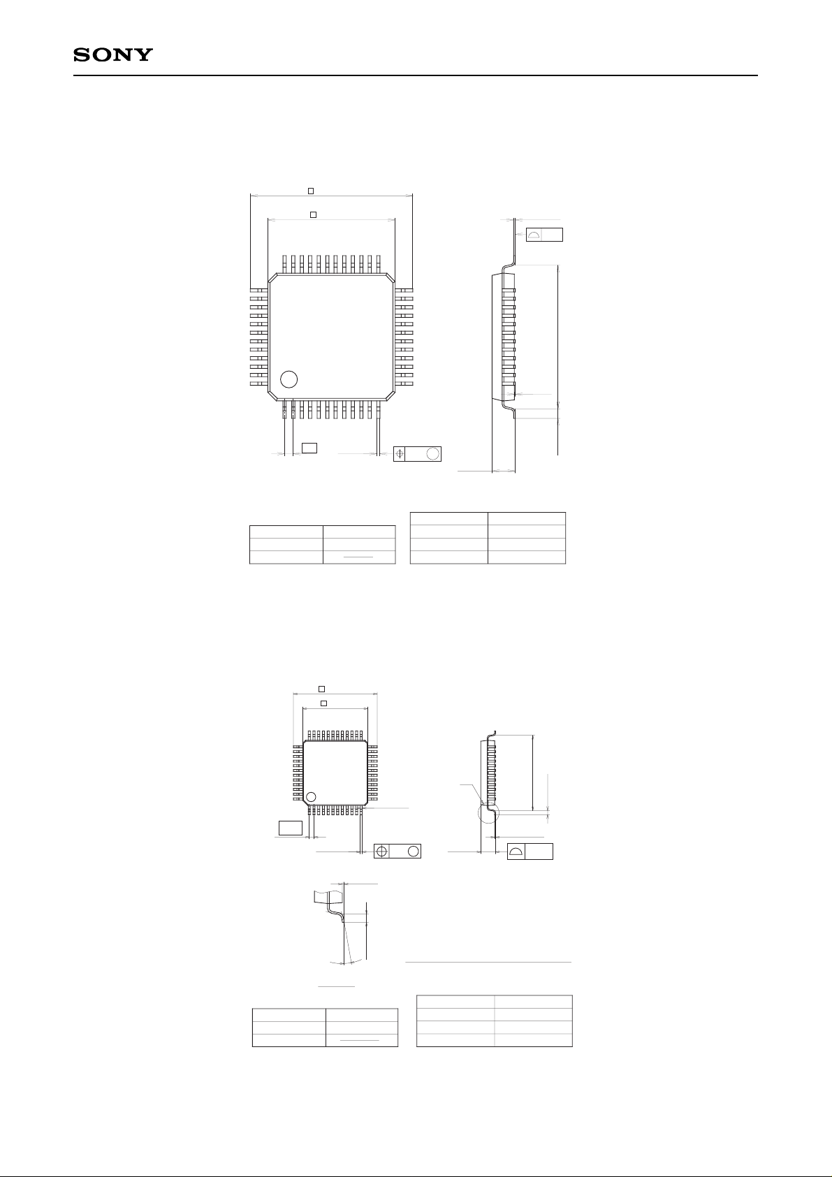
Package Outline Unit: mm
SONY CODE
EIAJ CODE
JEDEC CODE
M
PACKAGE STRUCTURE
PACKAGE MATERIAL
LEAD TREATMENT
LEAD MATERIAL
PACKAGE MASS
EPOXY RESIN
SOLDER / PALLADIUM
PLATING
42/COPPER ALLOY
48PIN QFP (PLASTIC)
15.3 ± 0.4
12.0 – 0.1
+ 0.4
0.8
0.3 – 0.1
+ 0.15
0.24
13
24
2536
37
48
1 12
2.2 – 0.15
+ 0.35
0.9 ± 0.2
0.1 – 0.1
+ 0.2
13.5
0.15 – 0.05
+ 0.1
QFP-48P-L04
QFP048-P-1212
0.7g
0.15
SONY CODE
EIAJ CODE
JEDEC CODE
PACKAGE MATERIAL
LEAD TREATMENT
LEAD MATERIAL
PACKAGE MASS
EPOXY RESIN
PLATING
42/COPPER ALLOY
PACKAGE STRUCTURE
48PIN LQFP (PLASTIC)
9.0 ± 0.2
∗ 7.0 ± 0.1
1
12
13
24
25
36
37
48
(0.22)
0.18 – 0.03
+ 0.08
0.2g
LQFP-48P-L01
LQFP048-P-0707
(8.0)
0.5 ± 0.2
0.127 – 0.02
+ 0.05
A
1.5 – 0.1
+ 0.2
0.1
SOLDER/PALLADIUM
NOTE: Dimension “∗” does not include mold protrusion.
0.1 ± 0.1
0.5 ± 0.2
0° to 10°
DETAIL A
0.13
M
0.5
CXA1202R
CXA1202Q-Z
NOTE : PALLADIUM PLATING
This product uses S-PdPPF (Sony Spec.-Palladium Pre-Plated Lead Frame).
 Loading...