

Page 1
8-bit 250 MSPS Flash A/D Converter
Description
The CXA1166K is an 8-bit ultrahigh-speed flash
A/D converter IC capable of digitizing analog signals
at a maximum rate of 250 MSPS. The digital I/O
level of this A/D converter is compatible with the
ECL 100K/10KH/10K.
This IC is pin-compatible with the conventional
CXA1076AK/CXA1176K/CXA1176AK, and can
replace the conventional models easily. Compared
with the conventional models, the CXA1166K has a
greatly improved performance because of the new
circuit design and carefully considered layout.
CXA1166K
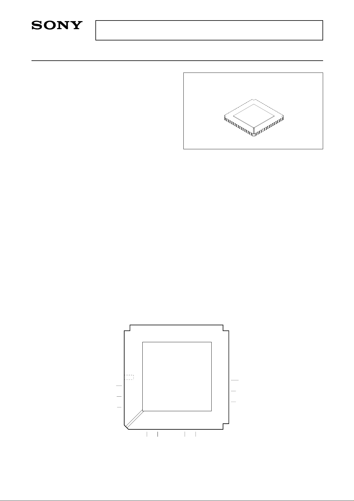
68 pin LCC (Ceramic)
Structure
Bipolar silicon monolithic IC
Features
• Differential linearity error: ±0.5 LSB or less
• Integral linearity error: ±0.5 LSB or less
• Built-in integral linearity compensation circuit
• Ultrahigh-speed operation with maximum conver-
sion rate of 250 MSPS
• Low input capacitance: 18pF
• Wide analog input bandwidth: 250MHz (full-scale
input, standard)
• Single power supply: –5.2V
• Low power consumption: 1.4W (Typ.)
• Low error rate
• Good temperature characteristics
• Capable of driving 50Ω loads
Pin Configuration (Top View)
Pins without name are NC pins (not connected internally).
EE
IN1
IN1
AGND
V
V
AGND
AV
VRT
VRTS
AVEE
AVEE
LINV
OR
OR
D0
D0
D1
D1
DV
AV
60
59
58
61
62
EE
63
64
65
66
67
68
1
2
3
4
5
6
7
EE
8
9
57
10
11
12
13
D2
D2
56
14
D3
55
15
D3
AGND
54
53
16
17
DGND2
DGND2
Applications
• Digital oscilloscopes
• Other apparatus requiring ultrahigh-speed A/D
conversion
RM
IN2
IN2
V
52
18
DGND1
AGND
V
51
50
19
20
D4
D4
V
49
21
D5
AGND
48
47
22
23
D5
45
44
46
24
AGND
43
EE
AV
42
41
VRB
40
VRBS
39
AVEE
38
AVEE
37
36
CLK
35
CLK
34
MINV
33
D7
32
D7
31
D6
30
D6
29
EE
DV
28
27
25
26
Sony reserves the right to change products and specifications without prior notice. This information does not convey any license by
any implication or otherwise under any patents or other right. Application circuits shown, if any, are typical examples illustrating the
operation of the devices. Sony cannot assume responsibility for any problems arising out of the use of these circuits.
– 1 –
E90406-ST
Page 2

Absolute Maximum Ratings (Ta = 25°C)
• Supply voltage AVEE, DVEE –7 to +0.5 V
• Analog input voltage VIN –2.7 to +0.5 V
• Reference input voltage VRT, VRB, VRM –2.7 to +0.5 V
| VRT – VRB | 2.5 V
• Digital input voltage MINV, LINV, CLK, CLK –4 to +0.5 V
| CLK – CLK | 2.7 V
• VRM pin input current IVRM –3 to +3 mA
• Digital output current ID0 to ID7, IOR, ID0 to ID7, IOR –30 to 0 mA
• Storage temperature Tstg –65 to +150 °C
Operating Conditions Min. Typ. Max. Unit
• Supply voltage AVEE, DVEE –5.5 –5.2 –4.95 V
AVEE – DVEE –0.05 0 0.05 V
AGND – DGND –0.05 0 0.05 V
• Reference input voltage VRT –0.1 0 0.1 V
VRB –2.2 –2.0 –1.8 V
• Analog input voltage VIN VRB VRT
• Operating temperature Tc –20 100 °C
CXA1166K
– 2 –
Page 3
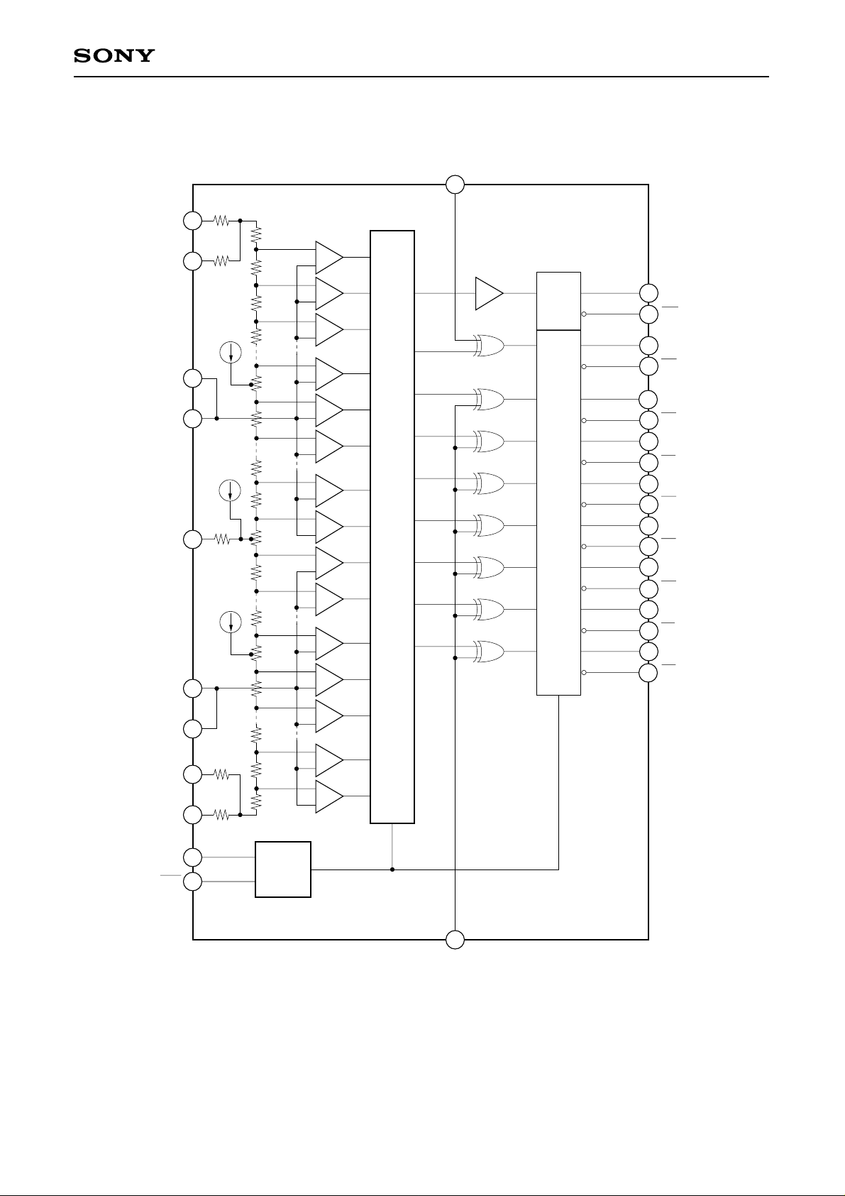
Block Diagram
VRTS
CXA1166K
MINV
33
r1
RT
V
64
r2
65
r/2
r
Comparator
0
VIN1
VRM
VIN2
VRBS
VRB
55
52
50
54
49
39
40
2
3
31
32
29
30
21
22
19
20
14
15
12
13
6
7
4
5
OR
OR
D7 (MSB)
D7
D6
D6
D5
D5
D4
D4
D3
D3
D2
D2
D1
D1
D0 (LSB)
D0
63
1
2
•
•
•
r
r
r
64
r
65
126
127
128
•
•
•
OUTPUT
ENCODE LOGIC
r
r
r3
r
r
129
191
•
•
•
r
r
192
r
193
254
255
•
•
•
r
r
4
5
r
r
r/2
CLK
CLK
35
34
CLOCK
DRIVER
1
LINV
– 3 –
Page 4
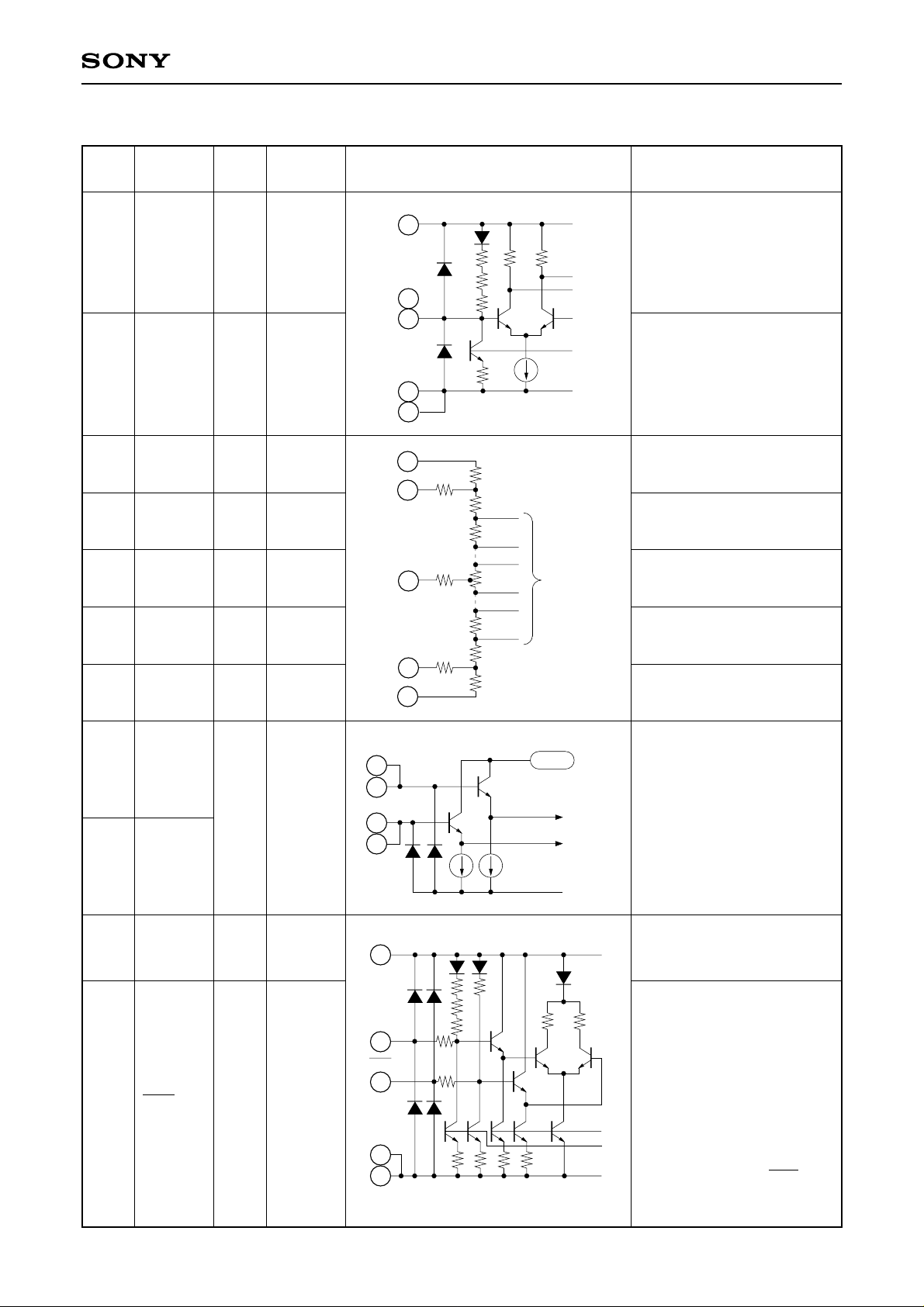
Pin Description
CXA1166K
Pin
No.
Symbol I/O
Standard
voltage level
1 LINV I ECL
33 MINV I ECL
64 VRT I0V
65 VRTS O0V
52 VRM IVRB/2
VRT
VRTS
VRM
Equivalent circuit Description
DGND1
18
LINV
1
or
33
MINV
r
r
r
–1.3V
Polarity selection other than
MSB and overrange.
(Refer to the table of input
voltage vs. Digital output)
Low level is maintained with
left open.
Polarity selection for MSB
(Refer to the table of input
DV
64
28
65
25
EE
8
r
r
r⁄2
r
r
1
To
Comparator
r2
r3
voltage vs. Digital output)
Low level is maintained with
left open.
Reference voltage
(Top) (0V typ.)
Reference voltage sense
(Top)
Reference voltage mid-point.
Can be used for linearity
compensation.
39 VRBS O –2V
VRBS
39
40 VRB I –2V Reference voltage (Bottom)
54
VIN1
55
VRTS
I
to
VRBS
49
VIN2
50
35
34
CLK
CLK
I
I
ECL
ECL
VRB
VIN1
54
55
49
50
VIN2
DGND1
18
CLK
35
CLK
34
40
r
r
4
r ⁄2
r5
43, 48, 51, 53, 56, 61
AGND
To Comp
0 to 127
128 to 255
r
r
r
r
Reference voltage sense
(Bottom)
Analog input.
Pins 49, 50 and Pins 54, 55
should be connected
externally.
CLK input
Complementary CLK input.
ECL threshold potential
(–1.3V) is maintained with
left open.
The complementary input is
recommended for stable
operation at high speed
DV
28
EE
8
r r
though the operation only
with the CLK input is
possible when the CLK
input is left open.
– 4 –
Page 5
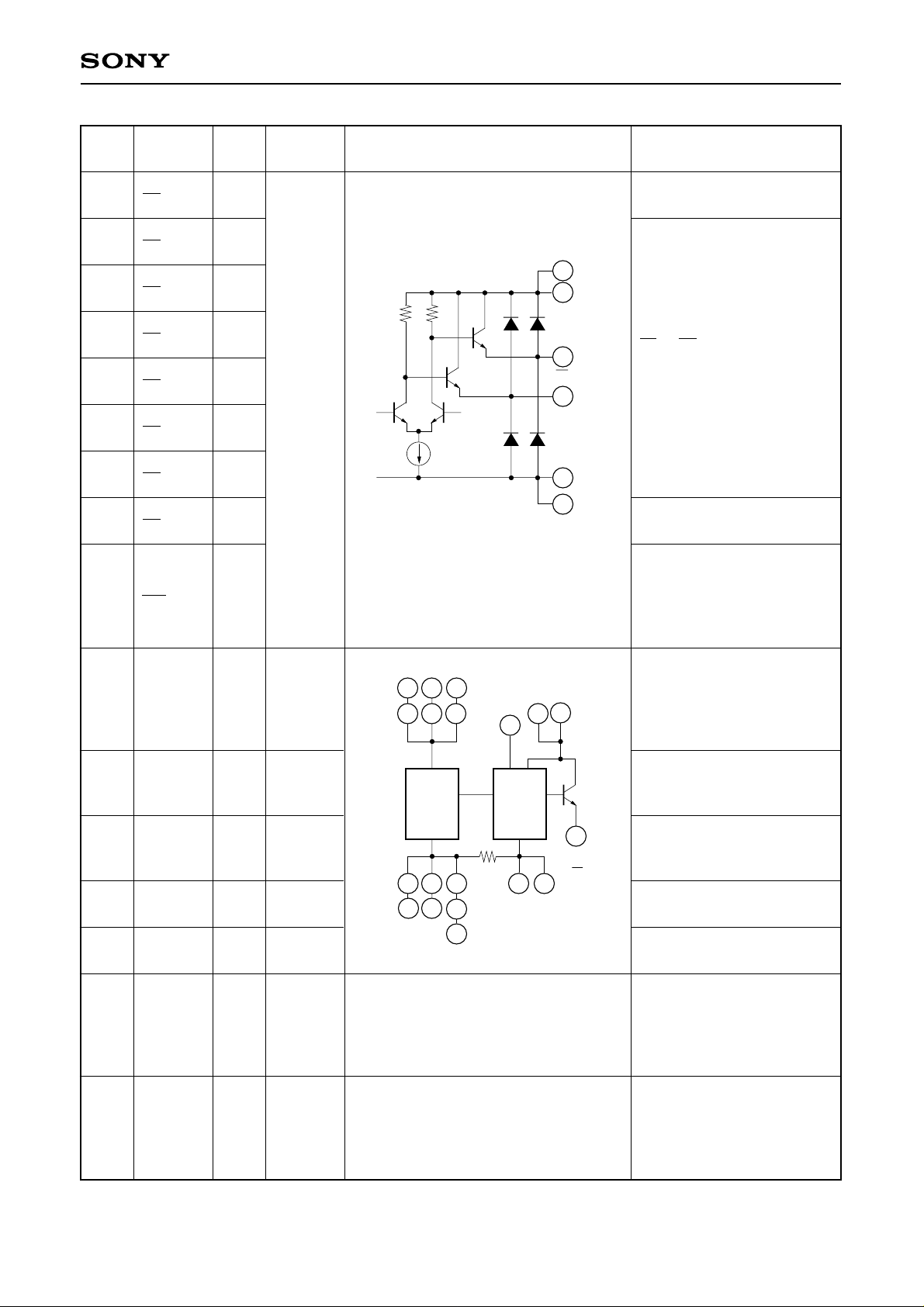
CXA1166K
Pin
No.
31
32
29
30
21
22
19
20
14
15
12
13
6
7
4
5
2
3
Symbol I/O
D7
D7
D6
D6
D5
D5
D4
D4
D3
D3
D2
D2
D1
D1
D0
D0
OR
OR
O
O
O
O
O
O
O
O
O
Standard
voltage level
ECL
Equivalent circuit Description
MSB and complementary
MSB output
DGND2
16
17
D1 to D6: Output
D1 to D6: Complementary
output
LSB and complementary
DV
EE
Di
Di
8
28
LSB output
Overrange output;
Low level for overrange.
Overrange complementary
output;
High level for overrange.
37, 38,
42, 58,
62,66,
AVEE∗
67
43, 48,
51,53,
AGND∗
56,61
8
DVEE∗
28
18 DGND1
16
DGND2∗
17
41, 44,
45, 46,
47, 57,
NC
59, 60,
63
9, 10,
11, 23,
24, 25,
NC —
26, 27,
36, 68
–5.2V
0V
–5.2V
0V
0V
—
AGND
61
43
Internal
Analog
Circuit
42
62
AVEE
48
51
37
38
53
56
58
66
67
DGND1
4 to 6Ω
DGND2
18
Internal
Digital
Circuit
8
DV
16
EE
28
17
Analog supply.
Internally connected with
DVEE (resistance: 4 to 6Ω).
Analog ground.
Separated from DGND.
Digital supply.
Di
Di
Internally connected with
AVEE (resistance: 4 to 6Ω).
Digital ground
Digital ground for output
drive
No connected.
It is recommended to connect
these pins to AGND.
No connected.
It is recommended to connect
these pins to DGND.
∗ For stable operation, all of these pins must be connected on the corresponding PCB pattern.
– 5 –
Page 6
CXA1166K
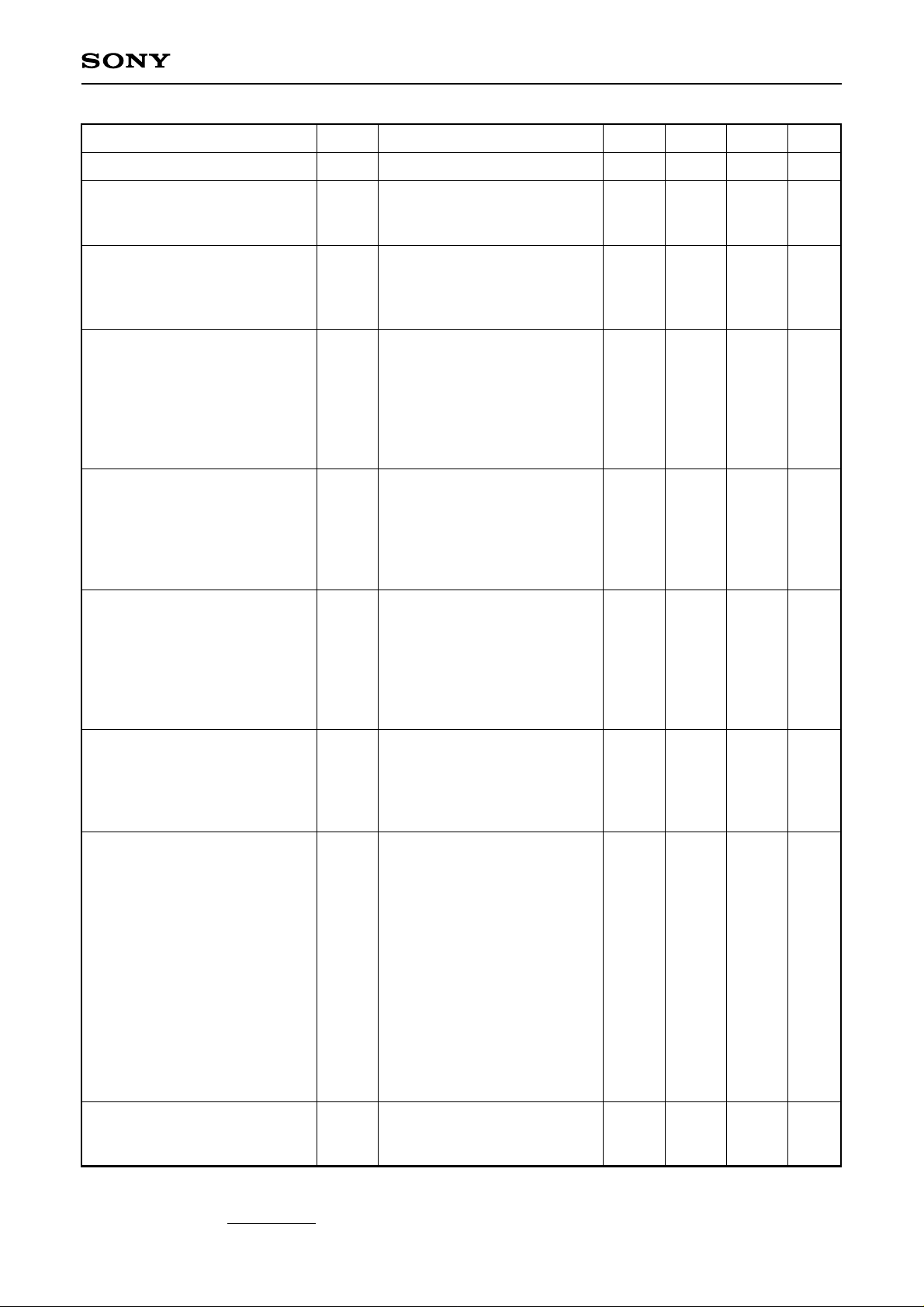
Electrical Characteristics (AVEE = DVEE = –5.2V, VRT, VRTS = 0V, VRB, VRBS = –2V, Ta = 25°C)
Item
Resolution
DC characteristics
Integral linearity error
Differential linearity error
Analog input
Analog input capacitance
Analog input resistance
Input bias current
Reference inputs
Reference resistance
Residual resistance∗1r1
Digital inputs
Logic High level
Logic Low level
Logic High current
Logic Low current
Input capacitance
Symbol Condition Min. Typ. Max.
8
EIL
EDL
CIN
RIN
IIN
RREF
r1
r2
r3
r4
r5
r2
r3
r4
r5
VIH
VIL
IIH
IIL
VIN = –1V + 0.07Vrms
VIN = –1V
VIN = –1V
VIH = –0.8V
VIL = –1.6V
50
20
83
0.1
300
0.5
300
0.1
–1.13
0
–50
18
120
125
0.6
500
2.0
500
0.6
4
±0.5
±0.5
450
182
2.0
700
5.0
700
2.0
–1.50
70
50
Unit
bits
LSB
LSB
pF
kΩ
µA
Ω
Ω
Ω
Ω
Ω
Ω
V
V
µA
µA
pF
Switching characteristics
Maximum conversion rate
Aperture jitter
Sampling delay
Output delay
Clock High pulse width
Clock Low pulse width
Digital output
Logic High level
Logic Low level
Output rise time
Output fall time
Dynamic characteristics
Input bandwidth
SNR
Error rate
Differential gain error
Differential phase error
Fc
Taj
Tds
Tdo
TPW1
TPW0
VOH
VOL
Tr
Tf
SNR
DG
DP
RL = 50Ω to –2V
TPW1 + TPW0 = 4.0ns
}
RL = 50Ω to –2V
RL = 50Ω to –2V
RL = 50Ω to –2V
RL = 50Ω to –2V
VIN=2Vp-p
Input = 1kHz, FS
{
Clock = 250MHz
Input = 62.499MHz, FS
{
Clock = 250MHz
Input = 49.999MHz, FS
Error > 16LSB
{
Clock = 200MHz
Input = 62.499MHz, FS
Error > 16LSB
{
Clock = 250MHz
NTSC 40IRE mod.
}
ramp, Fc = 250MSPS
250
0.4
1.8
1.8
1.8
–1.00
200
44
30
1.4
2.5
0.6
0.6
10
1.0
0.5
9
46
35
MSPS
ps
2.4
3.2
–1.60
1.5
1.5
10
–8
10
ns
ns
ns
ns
V
V
ns
ns
MHz
dB
dB
TPS∗
TPS∗
%
deg
2
2
–9
–6
Power supply
Supply current
Power consumption∗
∗1 See Block Diagram.
∗2 TPS: Times Per Sample
∗3 Pd = IEE • VEE +
3
(VRT – VRB)
RREF
IEE
Pd
2
– 6 –
–360
–270
1.4
1.9
mA
W
Page 7
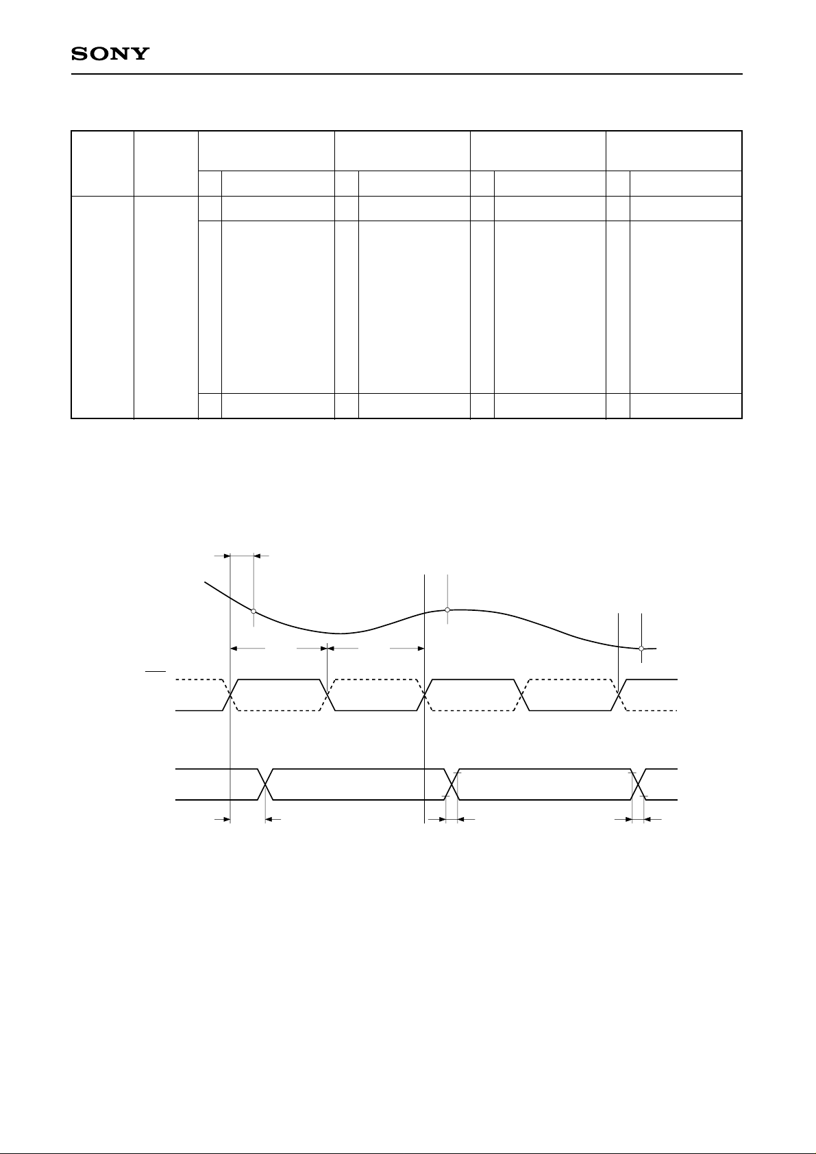
Input Voltage vs. Digital Output
CXA1166K
VIN∗
0V
Step
0
1
MINV 1
LINV 1
D7 D0 D7 D0 D7 D0 D7 D0
OR
0 0 0 …… 0 0
0
0 0 0 …… 0 0
1
0 0 0 …… 0 1
1
OR
0
1
1
0
1
1 0 0 …… 0 0
1 0 0 …… 0 0
1 0 0 …… 0 1
:
:
–1V
–2V
127
128
254
255
0 1 1 …… 1 1
1
1 0 0 …… 0 0
1
:
:
1 1 1 …… 1 0
1
1 1 1 …… 1 1
1
1 1 1 …… 1 1
1
1 1 1 …… 1 1
1
0 0 0 …… 0 0
1
:
:
:
:
0 1 1 …… 1 0
1
0 1 1 …… 1 1
1
0 1 1 …… 1 1
1
∗ VRT = VRTS =0V, VRM = –1V or Open, VRB = VRBS = –2V
Timing Diagram
1
0
OR
0 1 1 …… 1 1
0
0 1 1 …… 1 1
1
0 1 1 …… 1 0
1
:
:
1
1
:
:
:
:
1
1
1
:
:
0 0 0 …… 0 0
1 1 1 …… 1 1
:
:
1 0 0 …… 0 1
1 0 0 …… 0 0
1 0 0 …… 0 0
OR
0
1
1
1
1
:
:
1
1
1
0
0
1 1 1 …… 1 1
1 1 1 …… 1 1
1 1 1 …… 1 0
:
:
1 0 0 …… 0 0
0 1 1 …… 1 1
:
:
0 0 0 …… 0 1
0 0 0 …… 0 0
0 0 0 …… 0 0
Analog input
CLK
CLK
Digital output
Tds
Td
N
Tpw0Tpw1
20%
N + 1
80%
Tr Tf
NN – 1
80%
N + 2
N + 1
20%
– 7 –
Page 8
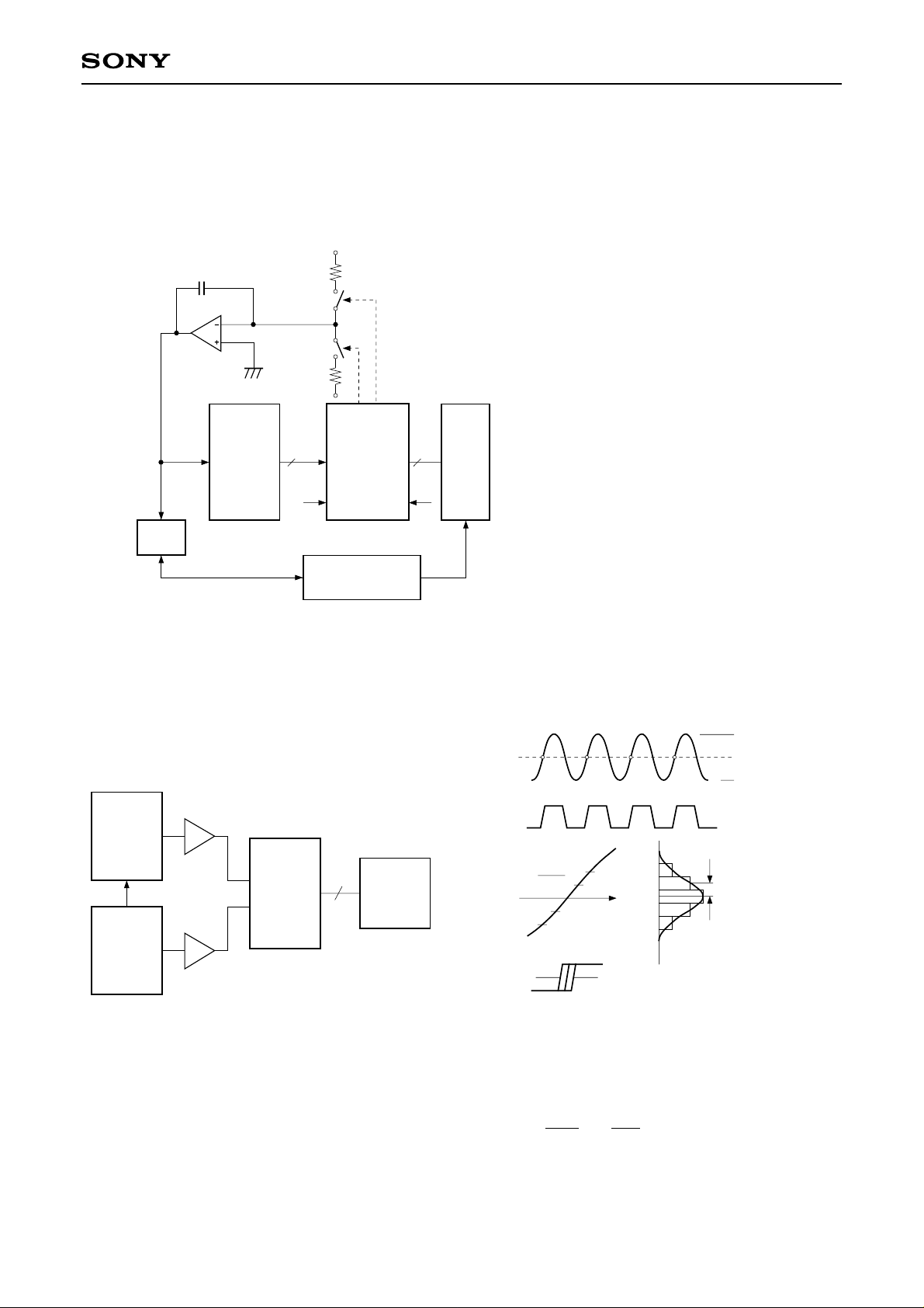
Electrical Characteristics Measurement Circuit
Integral Linearity Error Measurement Circuit
Differential Linearity Error Measurement Circuit
+ V
S2
S1:ON when A<B
S2: ON when A>B
S1
– V
A<B A>B
Comparator
DVM
V
IN
DUT
CXA1166K
8 8
A8
to
A1
A0
Controller
B8
to
B1
B0
“1 ”“0 ”
CXA1166K
Buffer
000•••0 0
to
111•••1 0
Sampling Delay Measurement circuit
Aperture Jitter Measurement circuit
60MHz
Amp
OSC1
φ:Variable
V
OSC2
60MHz
IN
fr
CLK
ECL
Buffer
CXA1166K
8
Logic
Analizer
1024
samples
Aperture Jitter Measurement Method
0V
VIN
CLK
∆
υ
∆ t
IN
V
CLK
When the distribution of the output codes is σ (unit: LSB) If
the maximum slew rate point is sampled with the clock signal
having the same frequency as that of the analog input signal,
Aperture jitter (Taj) is defined as follows:
Taj = σ/ = σ/ ( )
∆υ
∆t
129
128
t
127
126
125
Sampling timing fluctuation
( = aperture jitter)
256
× 2πf
2
–1V
–2V
σ (LSB)
– 8 –
Page 9
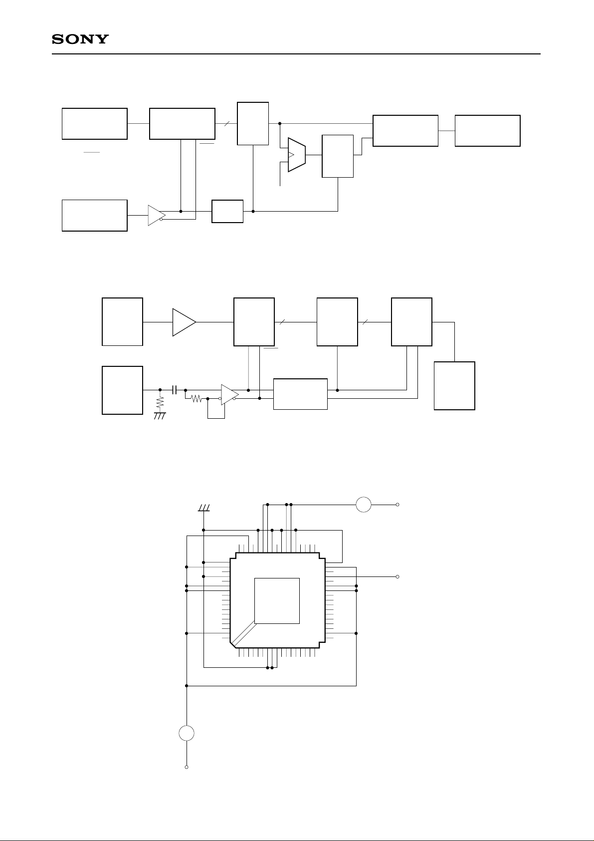
Error Rate Measurement Circuit
CXA1166K
Signal
Source
fCLK
– 1kHz
4
2Vp – p Sine Wave
Signal
Source
fCLK
Vin
CXA1166K
CLK CLK
8
1⁄16
ECL
Latch
Differential Gain Error Measurement Circuit
Differential Phase Error Measurement Circuit
NTSC
Signal
Source
SG (CW)
Amp
50
DUT
CXA1166K
CLK CLK
VBB
+
DAT A 16
8 8
Decimator
ECL
Latch
ECL
Latch
A
B
Comparator
A<B
(CX20202A – 1)
10bit
D⁄A
Pulse
Counter
Vector
Scope
Power Supply Current Measurement Circuit
Analog Input Bias Current Measurement Circuit
60
61
1
CXA1166K
9
10
A
EE
I
44
26
43
27
IIN
A
– 1V
– 2V
– 5.2V
– 9 –
Page 10

CXA1166K
Notes on Operation
• The CXA1166K is an ultra-high speed A/D converter featuring ECL level of input/output for the logic block. In
order to derive the most from its high-speed performance, the characteristic impedance should be matched
properly.
• The outputs are designed to drive a load terminated to –2V at 50Ω. An excellent transmission characteristic
can be yielded by designing the printed circuit board with a 50Ω characteristic impedance.
Yielding its top performance is difficult on the printed circuit board with a characteristic impedance of 100Ω or
more.
• The power supply and ground pattern greatly affect the characteristics of the converter. The higher the
frequency, the more important these connections become. The general precautions are as follows.
– Make the pattern of the power supply and ground as wide as possible. Using a ground plane inner layer by
using a multilayer printed circuit board is recommended.
– lsolate the AGND, DGND pins and the AVEE, DVEE from one another on the pattern in order to safeguard
against interaction. Connect the AGND and DGND pins at one place using a ferrite-bead filter to prevent
DC offset. The same processing is requited for the AVEE and DVEE pins.
• When mounting the A/D converter on the socket, use the one of shortest leads. The QFP socket, the type
name IC61-0684-048, manufactured by YAMAICHI ELECTRONICS CO., LTD. is recommended.
• The VIN analog input pins have somewhat large input capacitance (approximately 18pF) for high-frequency
circuits. In order to drive them with an excellent frequency response, it is necessary to safeguard against any
deterioration in performance resulting from parasitic capacitance and parasitic inductance by using a highcapacity drive circuit, keeping the wiring as short as possible, and using chip parts as resistors and
capacitors, for instance. The drive circuit shown in the Application Circuit has a virtually flat frequency
response up to approximately 170MHz. C89, R11 and C15 have been inserted mainly to expand the
bandwidth, while R10 has been inserted mainly to suppress operational amplifier oscillation and block
peaking of the frequency response. Since the optimal values of these elements differ depending on the
printed circuit board pattern and mounting condition of the A/D converter socket used, they must be
determined on the basis of experimentation.
• Connect all four VIN pins directly and as short as possible. Unlike the CXA1176, it is not necessary to insert
resistance of several ohms for each pin.
• The voltage at the VRT and VRB reference voltage pins and the reference voltage inside these pins differ
slightly due to residual resistance. VRTS and VRBS are provided to detect the reference voltage inside the pins.
The overrange reference voltage is 1/2 LSB down from VRTS; the lowest input voltage at which the output
code changes is 1/2 LSB up from VRBS.
• Provide adequate by-pass capacitors for VRT and VRB to protect them from high-frequency noise. Normally,
VRT is connected to AGND of an inner layer of the printed circuit board. Using a chip capacitor (approximately
0.1µF), make the by-pass from VRB to AGND as short as possible. C22 (1µ F), in the Application Circuit is for
suppressing the oscillation of the reference voltage generation circuit.
– 10 –
Page 11

CXA1166K
• Unlike the CXA1176, VRTS and VRBS are connected to the reference resistors via resistors of approximately
500Ω. Since these resistors may be eliminated in the future improved versions of this converter, use a
reference voltage generation circuit which is adaptable to their elimination. The reference voltage generation
circuit (the section composed of IC12_2, etc.) in the Application Circuit is recommended.
• Although VRM is provided to compensate for the integral linearity error, there is no need for such
compensation. It is recommended that it is kept open.
• OR and OR are output pins for indicating that the input is over range. They are not inverted by MINV or LINV.
• Noise in MINV and LINV results in misoperation, the cause of which is extremely difficult to track down. Keep
these pins open in cases where low level setting voltage alone is sufficient. When high level voltage input is
required, provide the shortest possible by-pass from them to DGND using chip capacitors (approximately
0.1 µ F) . Input voltages of –0.5V to –1.0V for high level and –1.6V to –2.5V for low level are recommend. Do
not make the direct connection to DGND when high level voltage is input.
• Inputting differential signals is recommended for the CLK and CLK clock input pins. Although operation is
possible by driving only the CLK pin, doing so involves the risk that the characteristics may become unstable
near the maximum speed. This is because the internal operation of the A/D converter depends on both clock
rise and fall.
• When the CLK pin is not used, by-pass it to DGND using a capacitor (approximately 0.1µF). At this time,
approximately –1.3V voltage will be generated at this pin. However, the driving capacity is too weak for this to
be used as the VBB threshold voltage. It cannot drive even one ECL input load.
• This converter is designed to be used at the clock duty cycle of 50%. The deviation from this condition will
subtly affect the performance of the A/D converter but the degree of the affection is not so great as to require
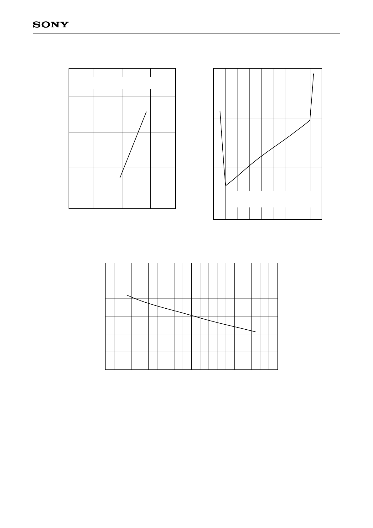
adjustment. The “Error rate vs. Clock duty cycle characteristics” graph shows an example of these changes
in the converter’s performance.
• Increasing chip temperature will cause the supply current and also the error rate to rise. Adding to these
reasons, in order to prolong the converter’s service life, provide an adequate means of cooling. See the
“Maximum conversion frequency vs. Temperature characteristics” and “Supply current vs. Temperature
characteristics” graphs. The reference data for thermal resistance is shown in the “Thermal resistance of the
converter mounted on a board” graph. Note that the actual thermal resistance will differ greatly depending on
the mounting conditions.
• Since the CXA1166K is a high-speed IC, take adequate measures to prevent electrostatic breakdown. For
further details on these measures, refer to “Precautions for IC Application” in Sony’s Data book.
• Sony’s SPECL series is used as the logic ICs in the Application Circuit to investigate the maximum
performance of the CXA1166K. For normal applications, lower speed logic ICs can be used according to the
applied frequency.
– 11 –
Page 12
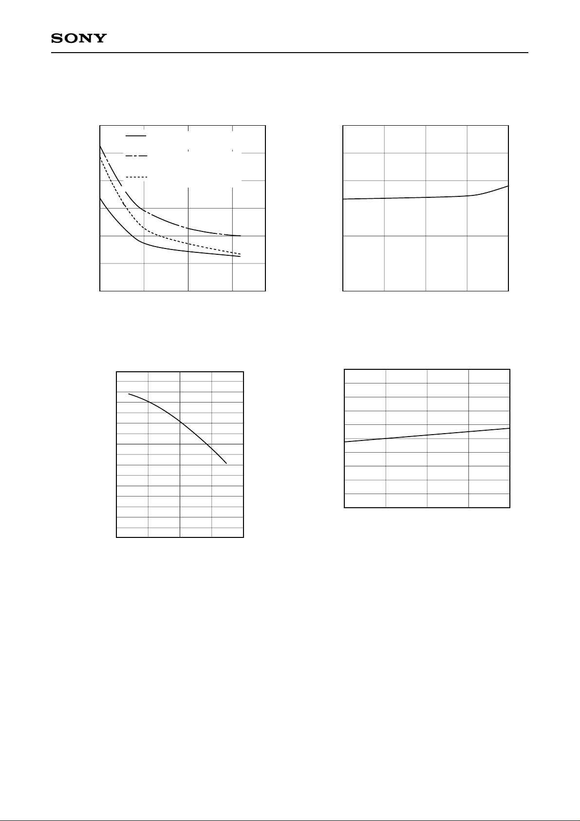
Example of Representative Characteristics
CXA1166K
Thermal resistance at on-board condition
50
Socket for YAMAICHI
ELECTRONICS IC61-0684-048
Socket for AMP173061-5
(without heat sink)
40
30
θ ja — Thermal resistance [°C/W]
0
Socket for AMP173257-3
(with heat sink)
1.0 2.0 3.0
Air velocity [m/s]
VIN pin input resistance vs.
Voltage characteristics
150
VIN pin input capacitance vs.
Voltage characteristics
25
20
15
— Input capacitance [pF]
IN
C
10
–2
V
IN — Input voltage [V]
VIN pin input current vs.
200
Voltage characteristics
–1
0–1.5 –0.5
125
µA]
100
IN [
I
100
Analog input resistance [kΩ]
–2.0
–1.5 –0.5
–1.0
V
IN — Input voltage [V]
0
0
–2.0
–1.0 0–1.5 –0.5
V
IN — Input voltage [V]
– 12 –
Page 13
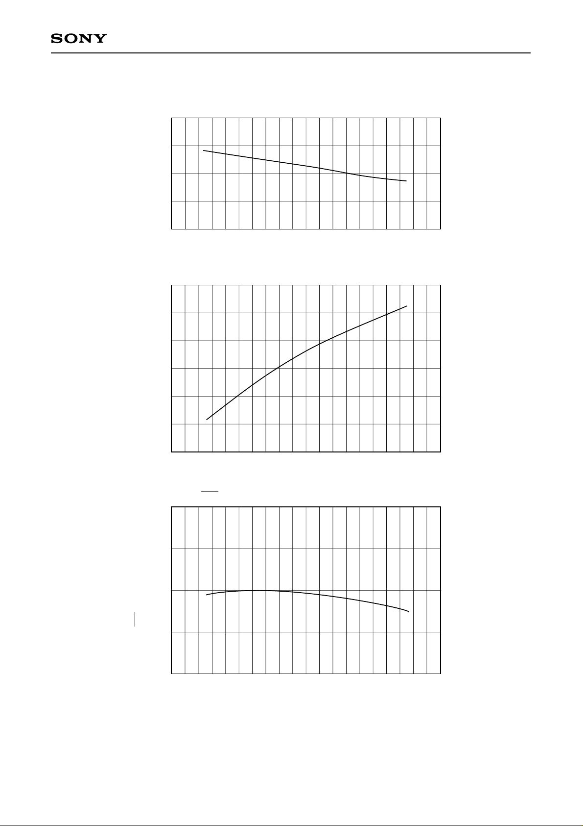
CXA1166K
— Input current [µA]
IN
V
200
150
100
–12
–14
–16
–18
50
VIN pin input current vs. Temperature characteristics
0
–50
0
Tc — Case temperature [°C]
50 100 150
Resistor string current vs. Temperature characteristics
–20
Resistor string current [mA]
–22
–24
–50
CLK open voltage vs. Temperature characteristics
–1.25
–1.3
–1.35
CLK open voltage [V]
–1.4
–1.45
–50
0
Tc — Case temperature [°C]
0
Tc — Case temperature [°C]
50 100 150
50 100 150
– 13 –
Page 14
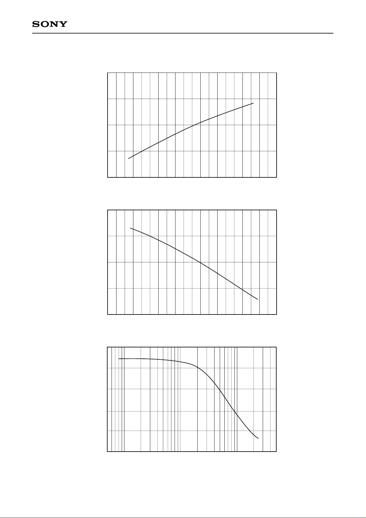
CXA1166K
[V]
OH
V
–0.7
–0.8
–0.9
–1.0
–1.1
–1.7
–1.8
–50
VOH vs. Temperature characteristics
0
Tc — Case temperature [°C]
50 100 150
VOL vs. Temperature characteristics
[V]
–1.9
OL
V
–2.0
–2.1
–50
50
45
40
SNR [dB]
35
30
0
Tc — Case temperature [°C]
50 100 150
SNR vs. Input frequency response characteristics
25
1 10 100
Input frequency [MHz]
– 14 –
Page 15
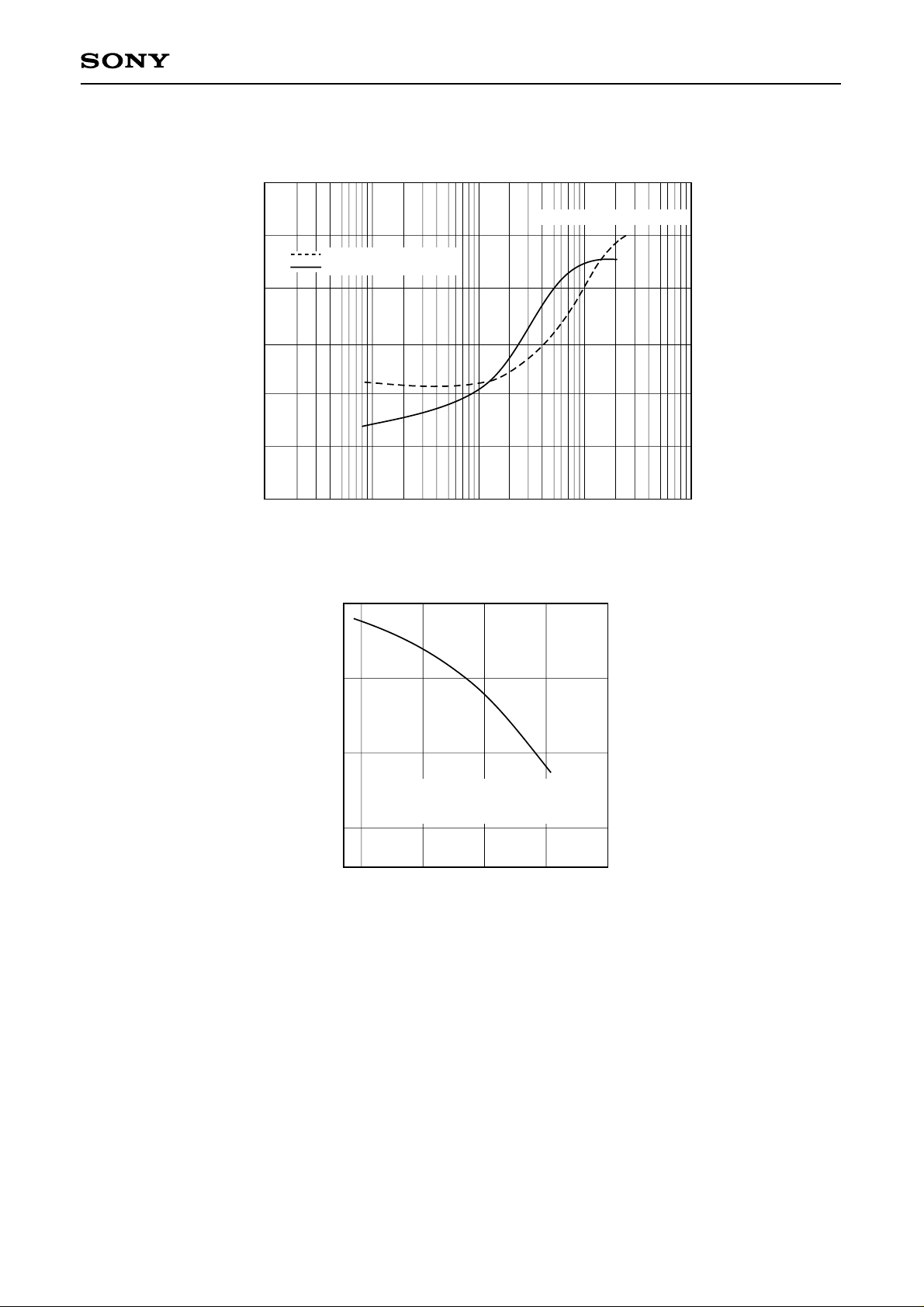
Harmonic distortion vs. Input frequency response characteristics
Clock frequency : 250MHz
–30
2nd harmonic distortion
3rd harmonic distortion
–40
–50
–60
Harmonic distortion [dB]
–70
–80
0.1
1
Input frequency [MHz]
10 100 1000
CXA1166K
300
250
200
CLK [MHz]
150
Maximum conversion rate vs.
Temperature characteristics
Error rate = 10–8TPS
Input frequency = CLK frequency/4 – 1kHz
16LSB or more error
75 12525–25
Ta — Ambient temperature [°C]
– 15 –
Page 16
CXA1166K
Input frequency = CLK frequency/4–1kHz
16LSB or more error
–
7
10
–
8
10
Error rate [TPS]
–
9
10
–
10
10
Error rate vs. Conversion rate
200
CLK frequency [MHz]
250 300
–
7
10
Error rate [TPS]
–
8
10
–
9
10
25
30
Error rate vs. Clock duty cycle
Input frequency = 125MHz, full-scale
Clock frequency = 250MHz
16LSB or more error
40 50
35 45 6055 65
CLK duty cycle [%]
70
–200
–250
–300
Supply current [mA]
–350
–50
Supply current vs. Temperature characteristics
0
Tc — Case temperature [°C]
50 100 150
– 16 –
Page 17
CXA1166K
8-bit, 250 MSPS ADC Evaluation Board
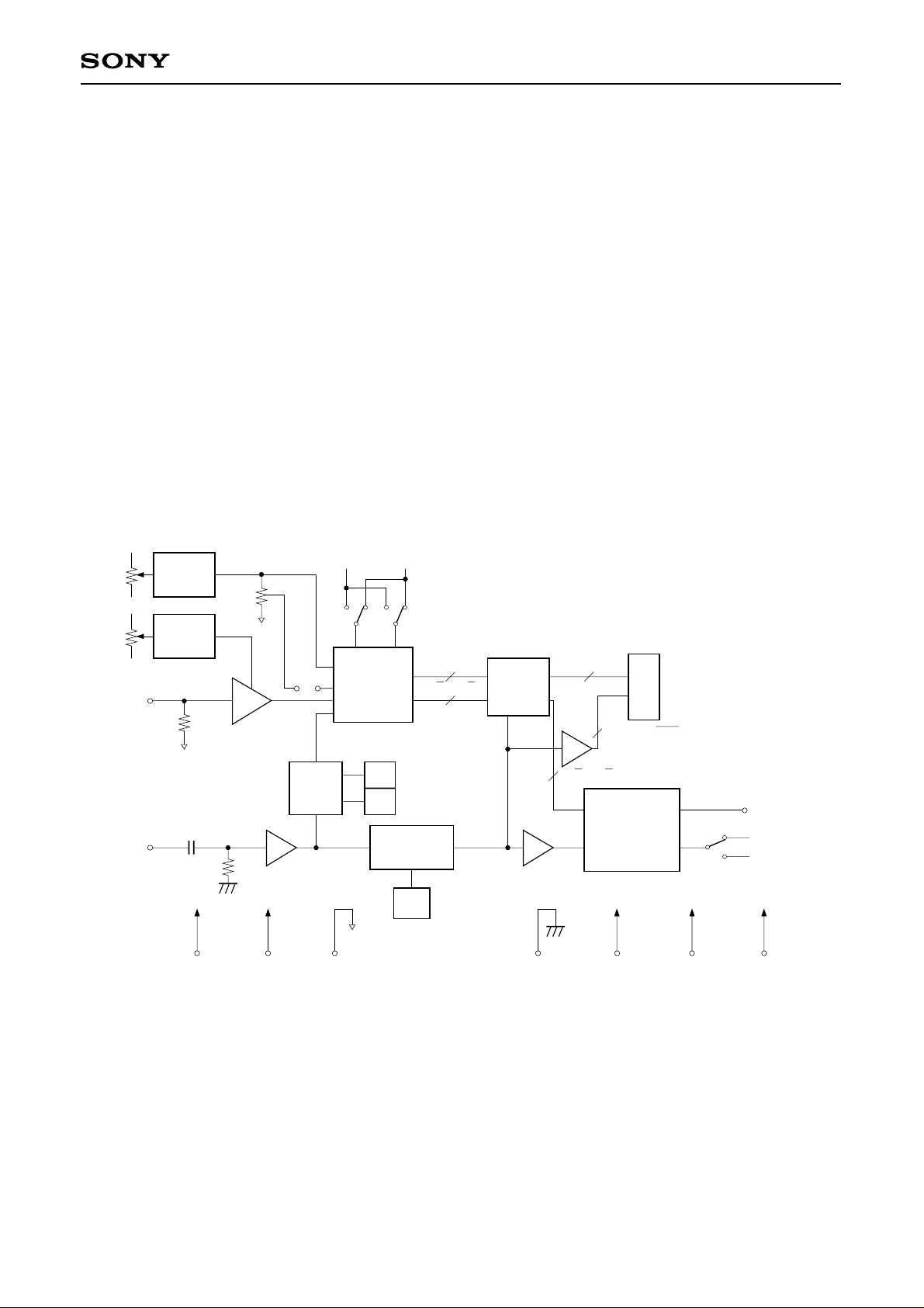
The CXA1166K PCB is a tool for customers to evaluate the performance of the CXA1166K (8-bit, 250MHz,
high-speed A/D converter). In addition to indispensable features such as the reference voltage generator, this
tool equips the input voltage offset generator, clock decimator, output date latches, 10-bit high-speed DAC,
and 20-pin cable connector for digital outputs. This evaluation board is designed to facilitate evaluation.
Features
• Resolution: 8 bits
• Maximum conversion rate: 250 MSPS
• Supply voltage: –5.2V, –4.5V, –2.0V, +5.0V
• Clock level converter: Sine wave to ECL level signal
• Reference voltage adjustment circuit for A/D converter
• Built-in clock frequency decimation circuit: 1/1 to 1/128
Fig. 1. Block Diagram
VR2
(2k)
R1
V
(2k)
AMP.IN
CLK
V
RB
– 2V
Vin
OFFSET
53
0.1µ
+ 5V (A) – 5.2V (A) – 5.2V (D) – 2V (D)DGND
R3
V
(2k)
(– 2)
51
SW4 SW5
LINV MINV
V
RB
J1
DELAY
AGND
VIN
CXA1166K
CLK
X
LH
SW2
SW1
DECIMATOR
SW3
8 (D7 to D0)
1/1 to 1/128
DATA
LATCH
CLK
8 (D7 to D0)8 (D7 to D0)
8 (D7 to D0)
CLK
DIGITAL OUT
(CONNECTOR)
2 (CLK.CLK)
D/A
CONVERTER
INV
D/A OUT
H
L
SW6
– 4.5V (D)
– 17 –
Page 18
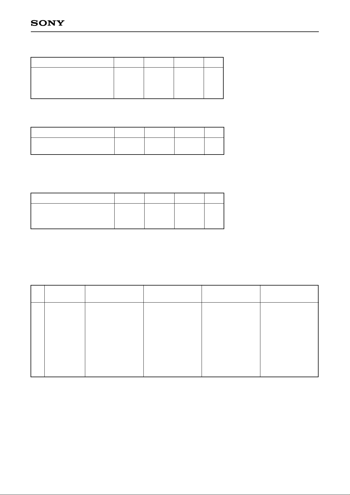
Supply Current
Item Min. Typ. Max. Unit
CXA1166K
–5.2V
+5.0V
–4.5V
–2.0
Analog Input (AMP. IN)
Item Min. Typ. Max. Unit
Input voltage (AMP.IN) ∗
Input impedance
Clock input (CLK)
Item Min. Typ. Max. Unit
Input voltage
(Peak to Peak)
Input impedance
–2.0
0.65
17
0.9
0.7
0.9
40
1.1
0.9
0V
50
(∗Adjustable with VR1)
2.0
50
A
mA
A
A
Ω
Vp-p
Ω
Digital output (Digital OUT)
ECL level
Output Code Table 1: ECL High level, 0: ECL Low level
VIN
MINV (SW5)
LINV (SW4)
0V
:
:
:
:
:
:
:
:
–2V
0
0
1 1 1 …… 1 1
1 1 1 …… 1 0
:
:
1 0 0 …… 0 0
0 1 1 …… 1 1
:
:
0 0 0 …… 0 1
0 0 0 …… 0 0
0
1
1 0 0 …… 0 0
1 0 0 …… 0 1
:
:
1 1 1 …… 1 1
0 0 0 …… 0 0
:
:
0 1 1 …… 1 0
0 1 1 …… 1 1
1
0
0 1 1 …… 1 1
0 1 1 …… 1 0
:
:
0 0 0 …… 0 0
1 1 1 …… 1 1
:
:
1 0 0 …… 0 1
1 0 0 …… 0 0
1
1
0 0 0 …… 0 0
0 0 0 …… 0 1
:
:
0 1 1 …… 1 1
1 0 0 …… 0 0
:
:
1 1 1 …… 1 0
1 1 1 …… 1 1
– 18 –
Page 19
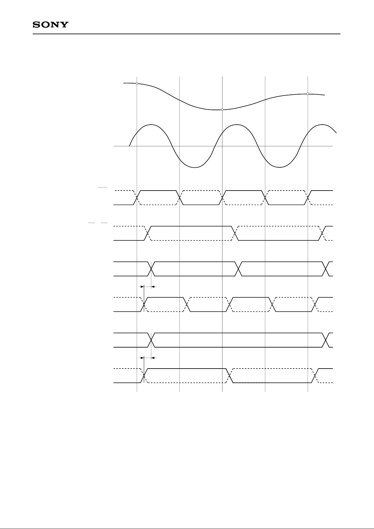
Fig. 2. Timing Diagram
CXA1166K
N
A/D input pin
(A MP. IN)
PCB input pin
A/D clock
A/D output
PCB output pin
(For 1/1 decimation)
PCB output pin
(For 1/1 decimation)
Vin
CLK
CLK
CLK
D7 to D0
D7 to D0
D7 to D0
CLKN
CLK
N + 2
N + 1
N – 1 N
N – 2 N – 1 N
Tdh
1.8ns
(Typ)
PCB output pin
(For 1/2 decimation)
PCB output pin
(For 1/2 decimation)
D7 to D0
Tdh
1.8ns
(Typ)
CLKN
CLK
Adjustment Methods and Notes on Operation
1) VIN Offset (VR1)
The volume to adjust the AMP. IN signal range (0V center assumed) with the A/D converter input range.
2) A/D Full Scale (VR2)
The volume to adjust A/D converter VRB voltage (–2V typ.).
3) Linearity (VR3)
The volume to adjust the VRM (linearity) voltage by shorting the J1.
– 19 –
NN – 2N – 4
Page 20
CXA1166K
4) D/A Full Scale (VR4)
The volume to adjust the bottom of D/A output full scale voltage (–1V typ.)
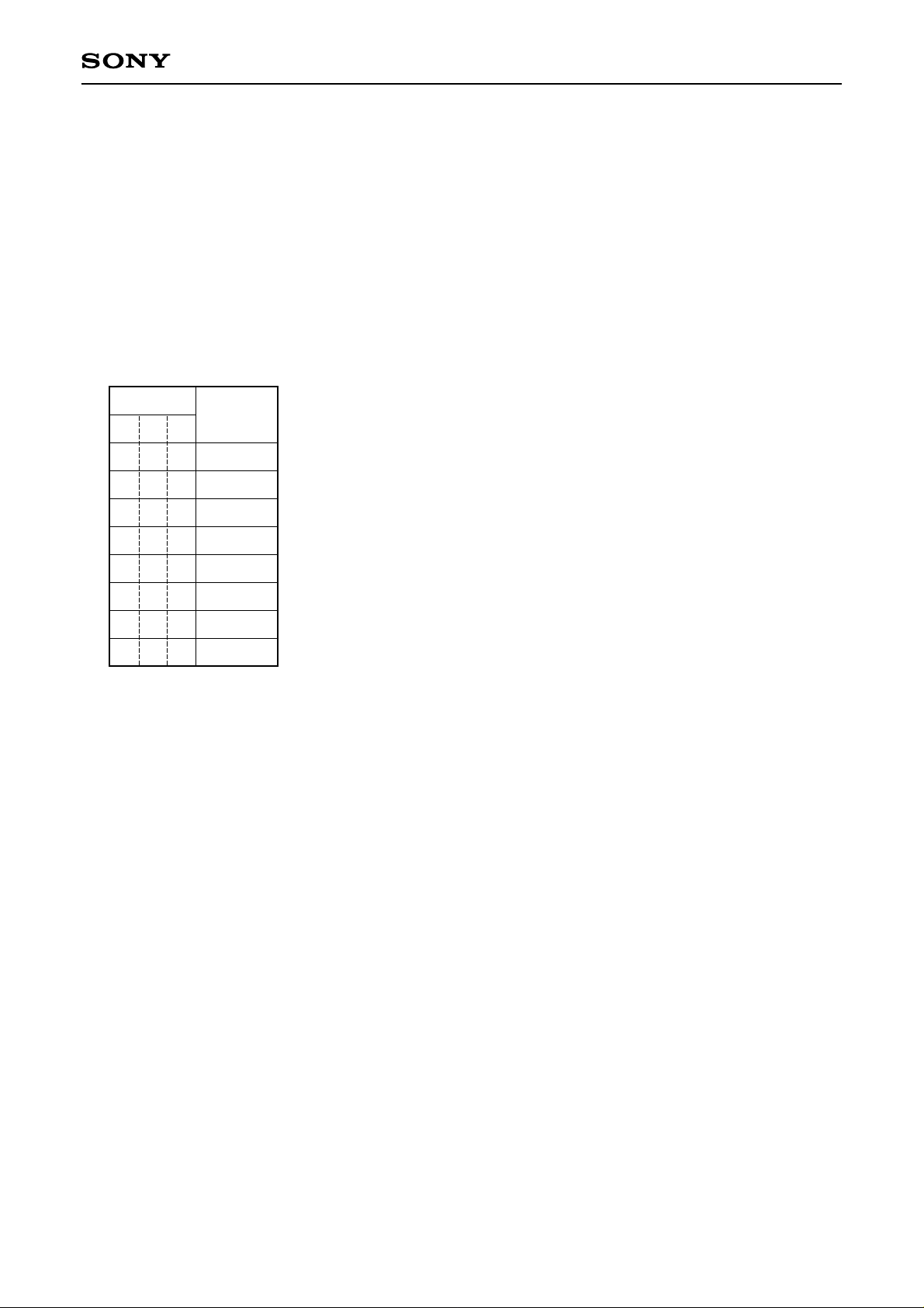
5) SW1 and SW2
Selection switches to adjust the clock delay. These switches enable clock delay to be stepped to any one of
128 settings (binary code of “0000000” to “1111111”) through binary input. Approximately 163ps is delayed
per one step. Normal evaluation requires the binary code of “0000000” (all of OFF), so that these switches
are not mounted for shipment.
6) SW3 (Decimation)
The switch to select clock frequency decimation. Selection settings are as follows.
3
L
L
L
L
H
H
H
H
SW3
2
L
L
H
H
L
L
H
H
Decimation
1
L
H
L
H
L
H
L
H
1/128
ratio
1/1
1/2
1/4
1/8
1/16
1/32
1/64
∗ H = ECL High level ; L = ECL Low level
7) SW4
The switch for LINV High/Low.
8) SW5
The switch for MINV High/Low.
9) SW6 (D/A INV)
The switch for D/A converter output inversion.
– 20 –
Page 21

CXA1166K
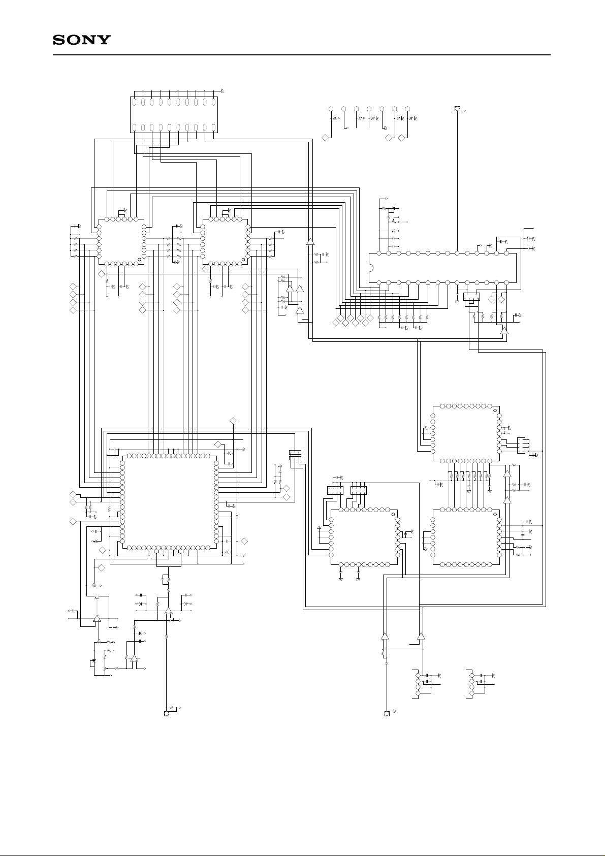
10) The waveform monitoring pins P6 through P39 are designed to make connection to GND easily in order to
reduce distortion when monitoring the waveform with an oscilloscope. As shown in the diagram below, the
distance between the measuring point and GND is 300mil, and each is equipped with a through hole of
1.2mm. When a Tektronix ground chip (part No. 013-1185-00) is mounted on the tip of a probe, the
signal – GND positions match.
φ1.2mm
Monitoring pointGND
Fig. 3.
11) D/A converter (IC9) input data (waveform monitoring pins P28 to P35) are the negative logic signals of the
decimated A/D converter outputs. Those are inverted again in the D/A converter so that the direction
(rise/fall) of reproduced waveform can agree with the A/D input signal's.
12) In order to maintain the accuracy of the reproduced waveform (waveform from A/D to D/A), set the
decimator such that the clock frequency of the D/A converter (IC9: CX20201A-1) is less than 100MHz.
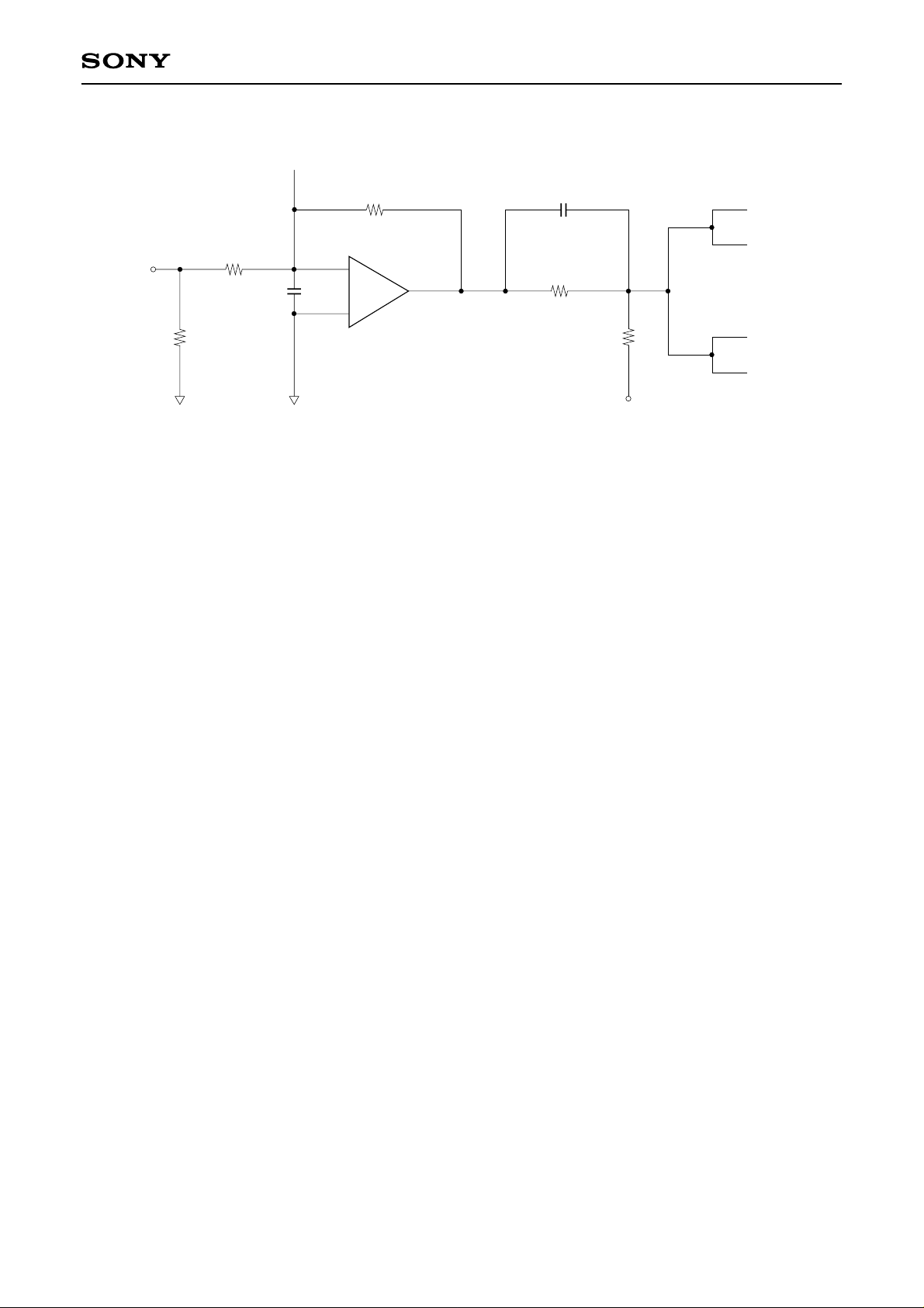
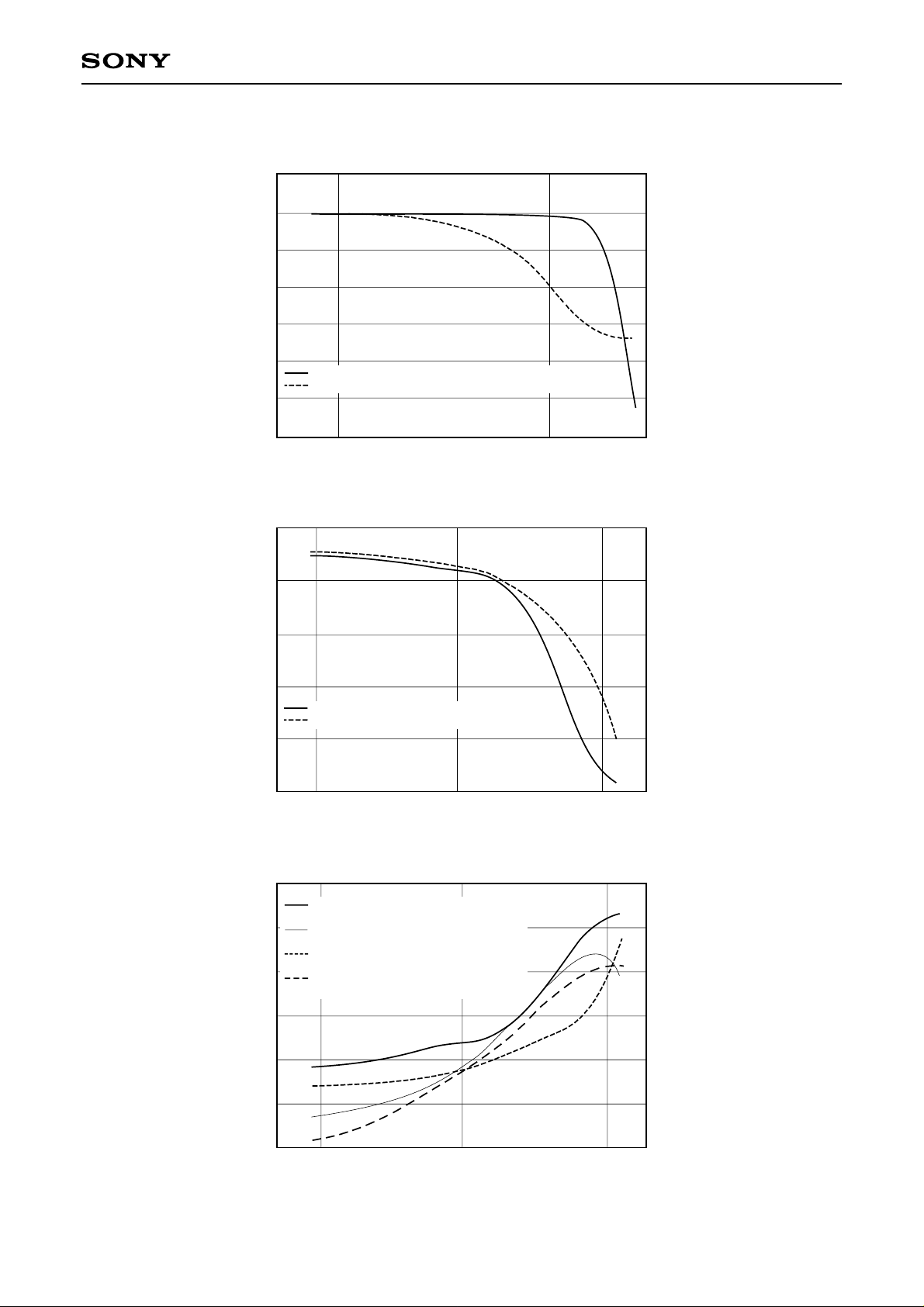
13) The input bandwidth weighs with the design of this PCB analog input circuit. Therefore, the SNR (signal-to-
noise ratio) should be less significant. The input circuit example to improve the SNR is shown in Fig.4. See
the measured data in Fig.s 6 to 8 for the SNR and the input circuit characteristics.
14) The part number of the digital output connector mounted on the PCB is KEL 8830E-020-170S. A
corresponding connector and cable assembly is JUNKOSHA KB0020MCG50B1.
– 21 –
Page 22
From offset circuit
CXA1166K
AMP. IN
560Ω
240Ω
3pF
68Ω
AGND AGND V
2
CLC409
3
6
5pF
30Ω
120Ω
Fig. 4. Example of SNR Improvement Circuit
RB (– 2V)
V
IN2
VIN2
VIN1
VIN1
– 22 –
Page 23
CXA1166K
2DGND1D0
Digital OUT
(LSB)
DGND
8
7
9
11
12
C40
0.1µ
∗
DGND
(D)
– 2V
51
R32
51
R31
51
R30
51
R29
D7N
P27
D7
P26
D6N
P25
D6
P24
10
CC
Q2
Q3
Q1N
13
Q1
14
D1
15
D1N
16
D2
17
D2N
18
CA
19
P38
CLKA
51
R62
C44
∗
(D)
– 2V
Q4
V
6
Q3M
Q2M
VCCA
Q4N
5
D4N
4
IC7
D4
3
CXB1109Q
D3N
2
D3
1
MR
VBBVCCA
VEECB
22
21
24
23
20
D5N
P23
DGND
DGND
C45
0.1µ
0.1µ
D5
∗
P22
(D)
– 4.5V
D4N
P21
D4
P20
12DGND11 D5
10DGND9D4
C42
0.1µ
∗
51
51
R36
R40
51
51
R39
R35
51
51
R38
R34
51
51
R37
R33
DGND
C41
0.1µ
∗
D3N
P19
D3
P18
D2N
P17
D2
P16
DGND
– 2V
20DGND19
18DGND17 CLK
16DGND15 D7
14DGND13 D6
CLKN
DGND
8
7
9
11
12
10
CC
Q2
Q3
Q1N
13
Q1
14
(D)
D1
15
D1N
16
D2
17
D2N
18
CA
19
P39
CLKB
51
R61
∗
(D)
– 2V
Q4
V
Q3M
Q2M
VCCA
Q4N
D4N
IC8
D4
CXB1109Q
D3N
D3
BB
VCCA
VEECB
MR
V
22
21
24
23
20
D1N
P15
DGND
DGND
C46
C47
0.1µ
0.1µ
D1
∗
P14
(D)
– 4.5V
D0N
P13
D0
P12
C43
0.1µ
∗
6
5
51
DGND
R44
4
3
2
1
(D)
– 2V
51
R43
51
R42
51
R41
51
R58
15
13
51
R57
14
16
IC5_2
20
19
18
17
51
R56
51
R55
12
11
C48
0.1µ
∗
DGND
23
24
(D)
– 2V
+ 5V (A)
AGND
AGND
33µ
C65
AGND
P42
+ 5V
7
8
IC5_4
2
1
C49
0.1µ
51
∗
R60
DGND
(D)
– 2V
51
R59
IC5_3
IC5_1
P34
P32
P35
P33
D1D3D5
D0D2D4
DGND
– 5.2V (A)
– 5.2V (D)
– 4.5V (D)
AGND
DGND
33µ
33µ
C64
P30
P31
P29
D6
33µ
C63
C62
DGND
P41
P40
EE
VTT
DV
( – 4.5)
AGND
IC10
TL431CP
270
R64
1k
R63
2k
VR4
1µ
C59
C58
0.1µ
C57
0.1µ
∗∗
26
28
27
REF
V
AVEE
AGND
D1D2D3D4D5D6D7D8D9
2
3
1
51
R45
R4651R4751R4851R4951R5051R5151R52
P28
D7
(D)
– 2V
C50
0.1µ
∗
– 2V (D)
DGND
DGND
33µ
C61
(A)
– 5.2V
25
24
NCNCNCNCNC
5
4
51
DGND
DGND
C51
0.1µ
∗
D/A OUT
AGND
(D)
1µ
C54
DGND – 5.2V
DGND
AGND
DGND
C55
0.1µ
22
21
23
20
19
NC
OUT
IC9
CXA20201
LSBNCNC
7
9
6
8
10
C60
0.1µ
INV
DGND
NORM
18
AGND
11
51
R66
17
DGND
12
SW6
P37
INV
CLKN
R5451R53
51
R65
IC5_5
∗
16
INV
CLKN
13
P36
CLK
36
15
EE
DV
CLK
14
45
DGND
C53
0.1µ
∗
C52
0.1µ
∗
51
DGND
(D)
– 2V
8DGND7D3
DGND
6DGND5D2
4DGND3D1
4
7
9
EE
DV
(D)
P8
– 5.2V
(D)
C38
0.1µ
∗∗
25
22
21
24
26
23
18
20
19
17
D5
C70
NCNCNC
0.1µ
NC
2728
DV
EE
D6
29
D6N
30
D7
31
D7N
32
MINV
33
CLKNCLKVRBS
51
R1351R12
(D)
C39
0.1µ
∗
GND – 2V
P5 P6 P7
AGNDAGND
∗
1µ
C22
AVEE
– 5.2V
P1
CLKN
34
CLK
35
NC
36
L2
AV
EE
BEAD
37
FERRITE
AV
EE
38
VRBS
39
V
RB
40
NC
4142
C23
0.1µ
AV
EE
43
NCNCNC
44
P4
C21
0.1µ
∗
VRT
Linearity
AGND
1k
VR3
Q1
2SA970
C10
0.1µ
∗
AGND
(A)
– 5V
874
6
TL4558
5
Full Scale
2k
VR2
R3
510
IC13
TL431CP
2k
VR1
IC12_2
Offset
AGNDAGND
(A)
+ 5.2V
(A)
C9
0.1µ
1k
R8
AGND – 5.2V
R6
1.3k
AGND
R5
240
(A)
– 5.2V
814
R4
22k
2
R2
11k
AGND
D4
NC
D5N
D4N
DGND1
DGND2
DGND2
IC6
CXA1166K
IN2
IN1
AGND
V
VIN2
AGND
VRMAGND
NC
47
46
45
V
54
49
53
51
52
50
48
J1
10
10p
R11
C15
∗
IC12_1
24
R10
IC11
R9
560
CLC404AJP
764
2
3
3P
C89
AGNDAGND
R7
240
AGND
68
R1
C12
0.1µ
∗∗
1µ
C11
C8
3.3µ
C7
0.1µ
TL4558
3
D3N
VIN1
55
∗
AGND
AGND
C14
C13
141516
D3
AGNDNCAV
56
0.1µ
1µ
DGND
11
12
13
10
NC
D2
NC
NC
D2N
EE
DV
D1N
D1
D0N
D0
ORN
OR
LINV
NC
AVEE
AVEE
VRTS
RT
V
NC
AV
EE
AGND
EE
NC
NC
60
57
58
59
AGNDAGND– 5.2V
(A)
AMP. IN
– 5.2V
P9
DGND
1µ
C37
C36
0.1µ
∗
9
8
7
6
5
4
3
2
1
6867
C34
0.1µ
∗
L1
66
BEAD
FERRITE
65
64
63
62
P2
61
1µ
C18
AGND
C19
0.1µ
∗
AGND
(A)
– 5.2V
LINV MINV
DGND
– 2V (D)
C35
0.1µ
∗
51
R2851R27
P11
P10
CXA1166K EVALUATION BOARD
NORM
INV
SW4 SW5
C26
0.1µ
∗
DGND
SW2
DGND
DELAY ADJ.
10
11
12
13
14
15
16
C5
C6
C16
∗
OR ORN
SW1
DELAY ADJ.
2
5
8
4
6
CBIAS
20
GND
C0C1C2C3C4
IC3
CXB1159Q
RBIAS
21
1
3
F2F3F4
F5
F1
32
F0
31
C24
0.1µ
∗
V
EE
30
DGND
EE
V
29
(D)
DIN
– 5.2V
DINB
27 28
V
REF
26
DINPB
DINPSWMR
24
25
22
23
IC1_1
17
28
51
R8
18 16
(D)
– 2V
C1
0.1µ
∗
VBB
EE
V
IC1
VCC
A
CXB1103Q
VCC
7
9
GND
GND
DGND
DOUT
DOUTB
DOUTP
DOUTPB
CAP
19
17
18
C17
0.01µ
∗
1000p
GND
DGND
CLK
8
DIH
DIG
LEN2
LEN1
10
QI
11
QIN
12
GND
CC
V
13
V
CCA
14
QO
15
QON
16
MR
DOG
DOH
18
19
17
51
51
R14
R15
(D)
– 2V
DGND
C33
0.1µ
∗
8
7
9
Q7
COUTN
10
COUT
11
VCCA
12
CC
V
13
CC
V
A
14
NC
15
DGND
MR
16
D6
D7
NC
19
17
18
IC1_2
17 15
C2
0.1µ
∗
22
DGND
C3
0.1µ
21
∗
IC5
(D)
– 4.5V
10
9
CXB1103Q
1
6
2
3
5
DIF
DIA
DIB
DIE
DIC
DID
NC
32
NC
31
C31
0.1µ
∗
VCCA
30
DGND– 4.5V
SW3
V
EE
DGND
29
DECIMATION
(D)
S2
S1
27 28
S0
26
DOA
DOB
DOC
DOD
25
22
24
23
R2051R1951R1851R1751R16
12
IC1_4
51
R21
24
C32
0.1µ
∗
4
22
22
21
10
9
23
C30
0.1µ
∗
DGND
IC1_3
35
2
1
3
Q0Q1Q2Q3Q4Q5Q6
S2
CIMN
32
S1
31
V
CCA
30
EE
V
29
C
CN
27 28
V
BB
26
D0D1D2D3D4
24
25
23
C5
0.1µ
∗
DGND
C4
0.1µ
∗
(D)
– 4.5V
R26
11
R25
R24
46
DGND
51
C29
0.1µ
∗
51
C28
0.1µ
∗
GND
(D)
– 2V
51
C27
0.1µ
∗
GND
DGND
C26
0.1µ
∗
(D)
– 4.5V
51
C25
0.1µ
R23
∗
GND
(D)
– 2V
51
R22
IC4
CXB1144Q
DOE
DOF
21
20
51
5
6
IC2
CXB1136Q
D5
20
21
VBB
EE
V
VCC
A
VCC
∗: CHIP CAPACITOR
Fig. 5. Schematic Diagram
– 23 –
Page 24
Characteristics
CXA1166K
2
0
– 2
– 4
– 6
Gain [dB]
– 8
– 10
– 12
5 10 100 300
Fig.6. Gain vs. Input frequency
Fig.5. CXA1166K PCB Schematic Diagram
Fig.4. Example of SNR Improvement Circuit
Input frequency [MHz]
Fig.7. SNR vs. Input frequency
50
45
40
SNR [dB]
35
30
25
– 20
– 30
– 40
– 50
– 60
Fig.5. CXA1166K PCB Schematic Diagram
Fig.4. Example of SNR Improvement Circuit
1 10 200100
Input frequency [MHz]
Fig.8. 2nd, 3rd Harmonic distortion vs. Input frequency
Fig.5. Schematic Diagram
(2nd Harmonic distortion)
Fig.5. Schematic Diagram
(3rd Harmonic distortion)
Fig.4. Example of SNR Improvement
Circuit (2nd Harmonic distortion)
Fig.4. Example of SNR Improvement
Circuit (3rd Harmonic distortion)
2nd, 3rd Harmonic distortion [dB]
– 70
– 80
1 10 200100
Input frequency [MHz]
– 24 –
Page 25
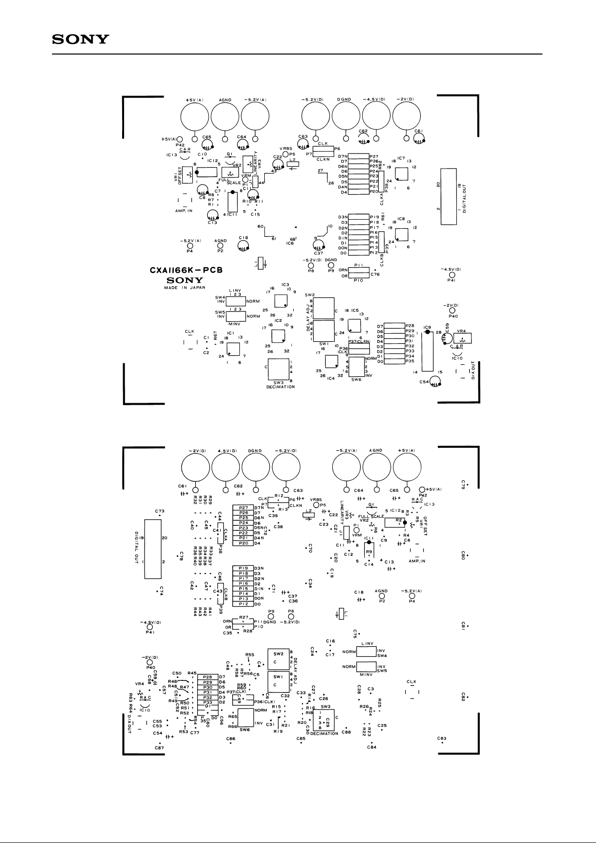
Parts Layout
CXA1166K
Component side
Soldering side
– 25 –
Page 26
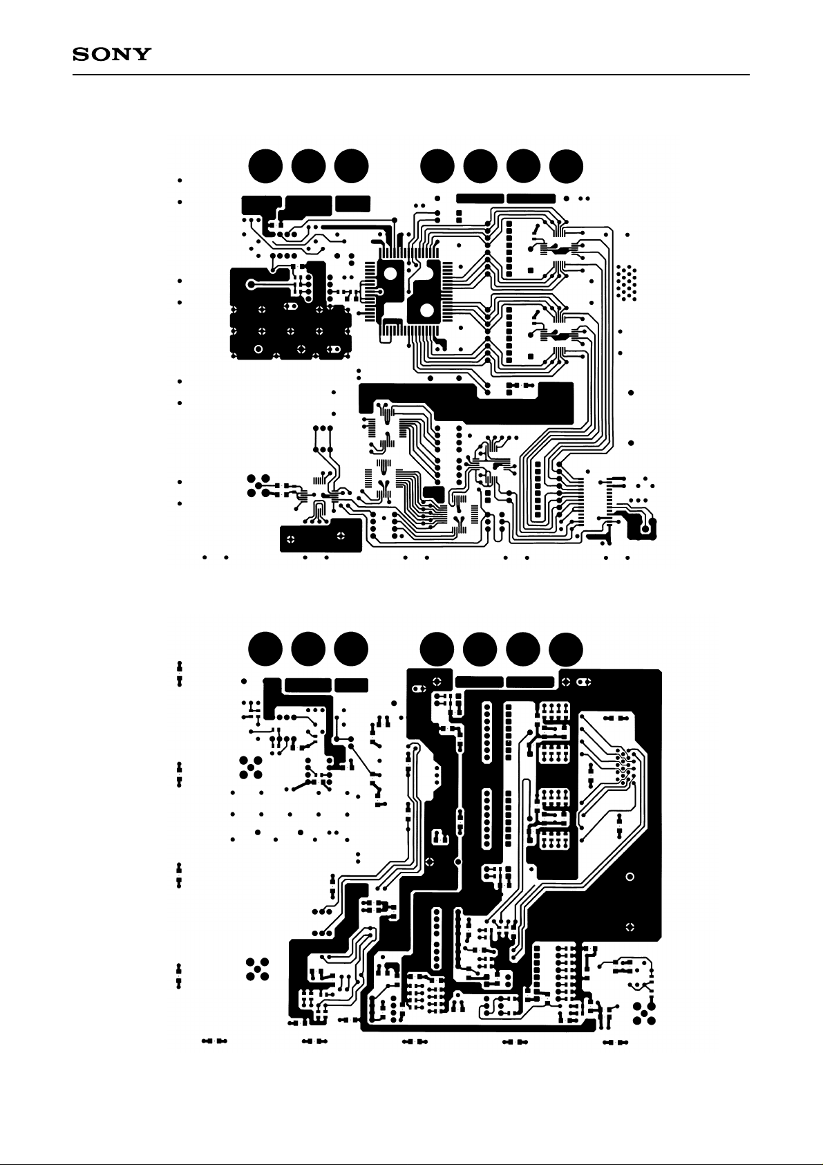
Printed Pattern
CXA1166K
Component side
Soldering side
– 26 –
Page 27
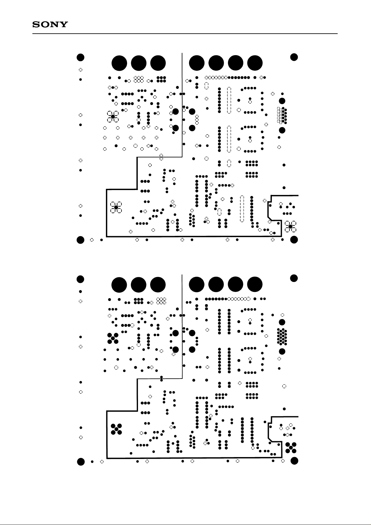
CXA1166K
GND layer (inner layer)
VEE layer (inner layer)
– 27 –
Page 28
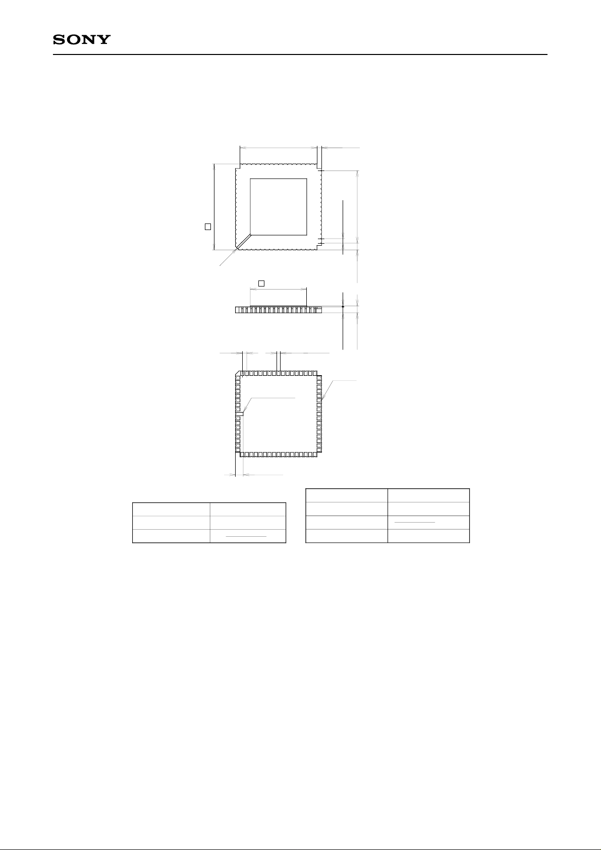
Package Outline Unit: mm
– 0.25
+ 0.38
CXA1166K
68PIN LCC (CERAMIC)
21.59 ± 0.2 1.27 ± 0.2
SONY CODE
EIAJ CODE
JEDEC CODE
24.13
C1
15.85 ± 0.2
1.27 0.915 ± 0.07
PIN NO.1
INDEX
2.16 ± 0.25
LCC-68C-01
∗QFN068-C-S950-A
20.32 ± 0.1
1.27 ± 0.1
1.9 ± 0.25
0.3
1.65 ± 0.18
1.95 ± 0.25
R0.2
PACKAGE STRUCTURE
PACKAGE MATERIAL
LEAD TREATMENT
LEAD MATERIAL
PACKAGE WEIGHT
CERAMIC
GOLD PLATING
3.7g
– 28 –
 Loading...