

Page 1
—1—
E91912B95-TE
Sony reserves the right to change products and specifications without prior notice. This information does not convey any license by
any implication or otherwise under any patents or other right. Application circuits shown, if any, are typical examples illustrating the
operation of the devices. Sony cannot assume responsibility for any problems arising out of the use of these circuits.
Absolute Maximum Ratings (Ta=25 °C)
• Supply voltage VCC 12 V
• Storage temperature Tstg –65 to +150 °C
• Allowable power dissipation
PD 1200 mW
Operating Conditions
• Supply voltage VCC 4.0 to 10.0 V
DVCC 3.5 to VCC V
• Operating temperature Topr –20 to +75 °C
Description
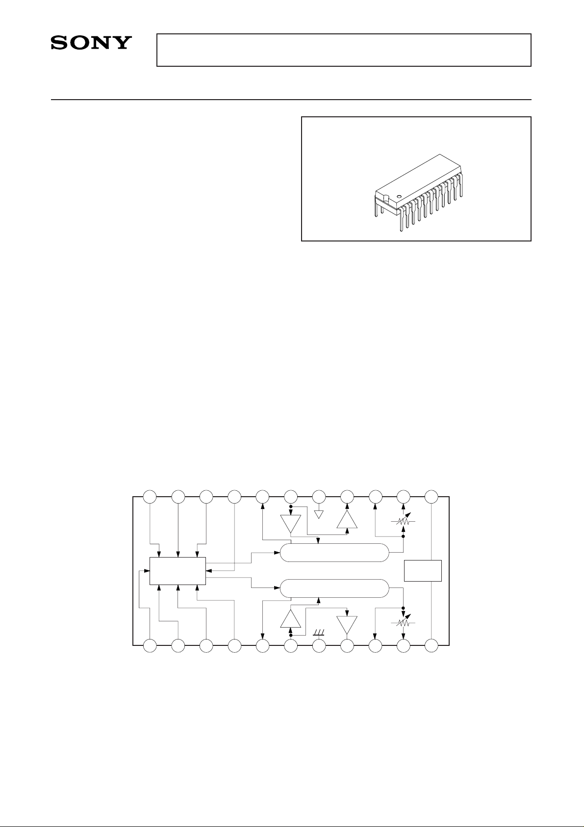
The CXA1352AS is a bipolar IC for graphic
equalizer use. All controls are DC performed while
the addition of single-potentiometers easily
composes a 2-channel graphic equalizer.
Features
• Microcomputer control possible
• Built-in electronic volume
• Built-in pseudo loudness function
• Built-in balance function
• Each channel corresponds to 5 elements
• 2 channels of FIX OUT and LINE OUT pins
Applications
Graphic equalizer for cassette tape recorder with
radio, mobile stereo and portable stereo
Structure
Bipolar silicon monolithic IC
2-channel 5 Elements Graphic Equalizer IC
22 pin SDIP (Plastic)
Block Diagram and Pin Configuration
1 2
3 4 5 6 7 8 9 10
11
1213141516171819202122
GRAPHIC EQUALIZER
GRAPHIC EQUALIZER
BIAS
VOLUME
VOLUME
CONTROL
14dB
14dB
29dB
29dB
1kHz
400Hz
100Hz
BAL
VOL
DC1
1N1
GND
LINE
OUT1
OUT1
(Fix)
OUT1
(VARIABLE)
4kHz
10kHz
DC2
IN2
VG
LINE
OUT2
OUT2
(FIX)
OUT2
(VARIABLE)
DV
CC
VCC
ISET
CXA1352AS
Page 2
—2—
CXA1352AS
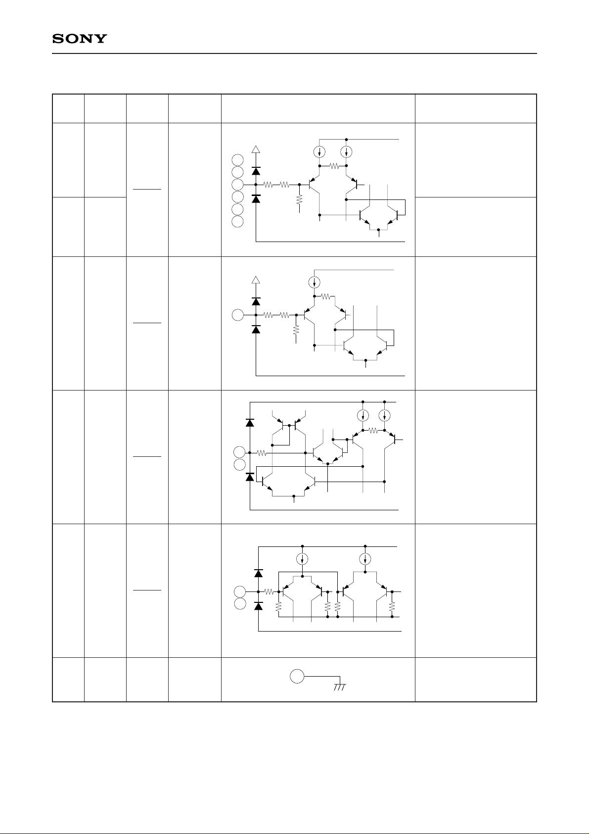
Pin Description
Pin
Symbol Voltage
I/O
Equivalent circuit Description
No. resistance
1
2
20
21
22
4
3
5
18
6
17
7
400 Hz
100 Hz
10 kHz
4 kHz
1 kHz
VOL
BAL
DC1
DC2
IN1
IN2
GND
DVCC
2
DVCC
2
VCC
2
VCC
2
GND
60 kΩ
60 kΩ
—
25 kΩ
1
2
4
20
21
22
DVCC
VCC
10k
147 40k
20k
GND
DVCC
VCC
9k
147 40k
20k
GND
3
18
VCC
147
30k
GND
5
6
17
VCC
147
50k
50k 1k5k
GND
7
Graphic equalizer control
pin
DC input
Volume control pin
DC input
Balance control pin
DC input
Connects the DC
feedback capacitor of the
LPF used in the 100 Hz
graphic equalizer
Signal input pin
GND pin
Page 3
—3—
CXA1352AS
Pin
Symbol Voltage
I/O
Equivalent circuit Description
No. resistance
8
15
9
14
10
13
11
L OUT1
L OUT2
F OUT1
F OUT2
OUT1
OUT2
ISET
VCC
2
VCC
2
VCC
2
1.3 V
0
0
0
0
VCC
147 27k
300
300
GND
8
15
14
VCC
147 30k
300
300
GND
9
13
VCC
147 20k
250
250
GND
10
VCC
147
300
GND
11
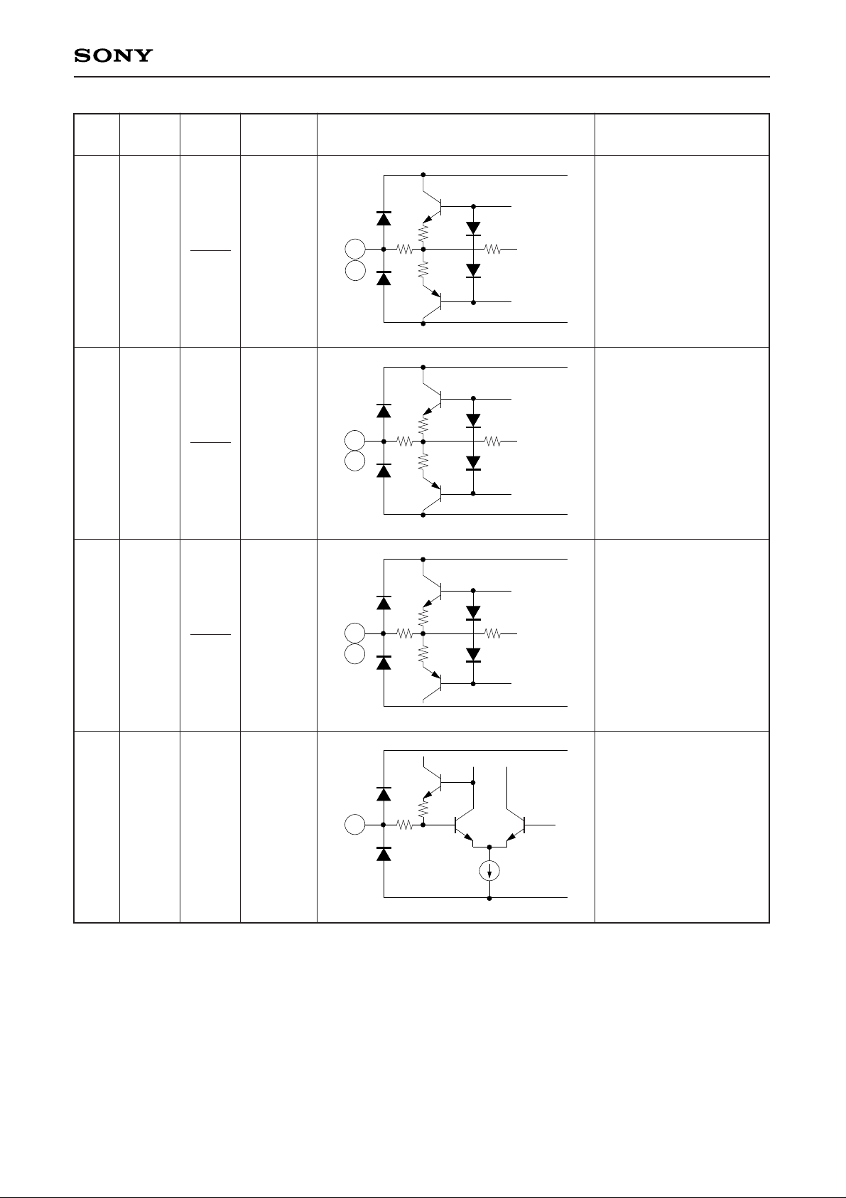
Line output pin
Fix output pin
Electronic volume output
pin
Reference current setting
pin
(for graphic equalizer)
Normally 160 kΩ resistor
is connected
Page 4
—4—
CXA1352AS
Pin
Symbol Voltage
I/O
Equivalent circuit Description
No. resistance
12
16
19
VG
VCC
DVCC
VCC
2
VCC
DVCC
20 kΩ
60 kΩ
VCC
147
40k
40k
300
GND
12
300
VCC
16
VCC
DVCC
GND
19
30k
30k
42k
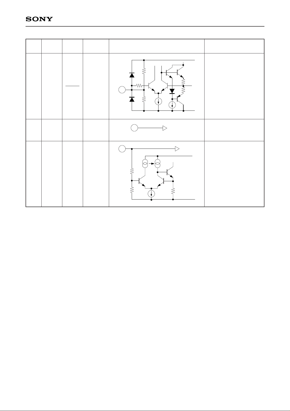
Signal reference voltage
pin
A capacitor is connected
for ripple rejection
Power supply pin
(operation)
Power supply pin (control)
Page 5
—5—
CXA1352AS
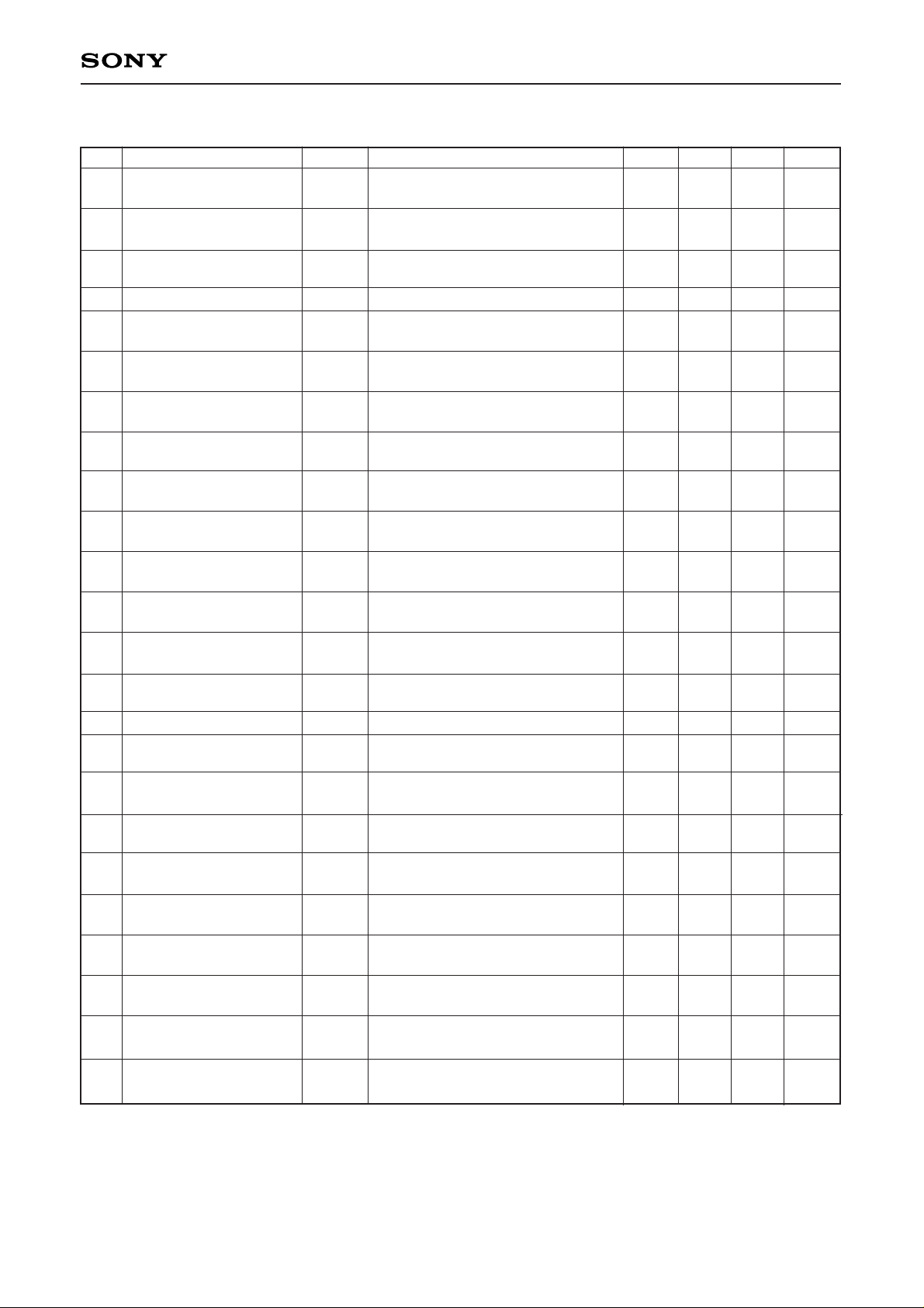
Electrical Characteristics (Ta=25 °C, VCC=8 V, DVCC=5 V)
No.
1
2
3
4
5
6
7
8
9
10
11
12
13
14
15
16
17
18
19
20
21
22
23
24
Item
Supply voltage
(operation)
Supply voltage
(control)
Current consumption
Reference input level
Reference output level
Reference LINE
output level
Reference FIX
output level
Graphic equalizer
setting frequency (1)
Graphic equalizer
setting frequency (2)
Graphic equalizer
setting frequency (3)
Graphic equalizer
setting frequency (4)
Graphic equalizer
setting frequency (5)
Graphic equalizer
frequency deviation
Maximum boost (1)
Maximum boost (2)
Maximum cut (1)
Maximum cut (2)
Total harmonic
distortion
Volume attenuation (1)
Volume attenuation (2)
Balance adjustment (1)
Balance adjustment (2)
Noise level
Output offset voltage
Symbol
VCC
DVCC
ICC
VIN
VOUT
VLINE
VFIX
GEQ1
GEQ2
GEQ3
GEQ4
GEQ5
∆ EQ
GEQB1
GEQB2
GEQC1
GEQC2
THD
VOL1
VOL2
BAL1
BAL2
VNOIS
VOFF
Test conditions
Graphic equalizer ALL FLAT,
Volume MID
Graphic equalizer ALL FLAT,
Volume MAX, f=1 kHz
f=1 kHz
Graphic equalizer ALL FLAT,
f=1 kHz
LPF cut off frequency (–3 dB)
BPF (1) central frequency
BPF (2) central frequency
BPF (3) central frequency
HPF cut off frequency (–3 dB)
Cut off frequency and central
frequency deviation
f=400 Hz, 1 kHz, 4 kHz
maximum boost
f=100 Hz, 10 kHz maximum boost
f=400 Hz, 1 kHz, 4kHz
maximum cut
f=100 Hz, 10 kHz maximum cut
RL=2 kΩ, Graphic equalizer
ALL FLAT, Volume MAX, f=1 kHz,
Reference +10 dB is input
Graphic equalizer ALL FLAT,
Volume MAX, f=1 kHz
Graphic equalizer ALL FLAT,
Volume MIN, f=1 kHz
Graphic equalizer ALL FLAT,
BAL=MAX,Volume MAX, f=1kHz
Graphic equalizer ALL FLAT,
BAL=MIN, Volume MAX, f=1kHz
Rg=5 kΩ, Graphic equalizer ALL
FLAT, Volume MAX, “A” WTG filter
Graphic equalizer ALL FLAT,
Volume MAX
Min. Typ. Max. Unit
4.0 — 10.0 V
3.5 — VCC V
8.0 12.0 16.0 mA
— –34.0 — dBm
–23.0 –20.0 –17.0 dBm
–6.5 –4.5 –2.5 dBm
–23.0 –20.0 –17.0 dBm
— 200 — Hz
— 400 — Hz
— 1.0 — kHz
— 4.0 — kHz
— 8.0 — kHz
–20 0 20 %
9.0 11.2 14.0 dB
8.0 10.7 14.0 dB
–13.0 –10.7 –8.5 dB
–12.0 –9.5 –7.0 dB
— 0.25 1.0 %
–1.5 0 1.5 dB
— –94.4 –80.0 dB
— 0 — dB
— –66 — dB
— –93.1 –88.0 dB
3.5 4.0 4.5 V
Page 6
—6—
CXA1352AS
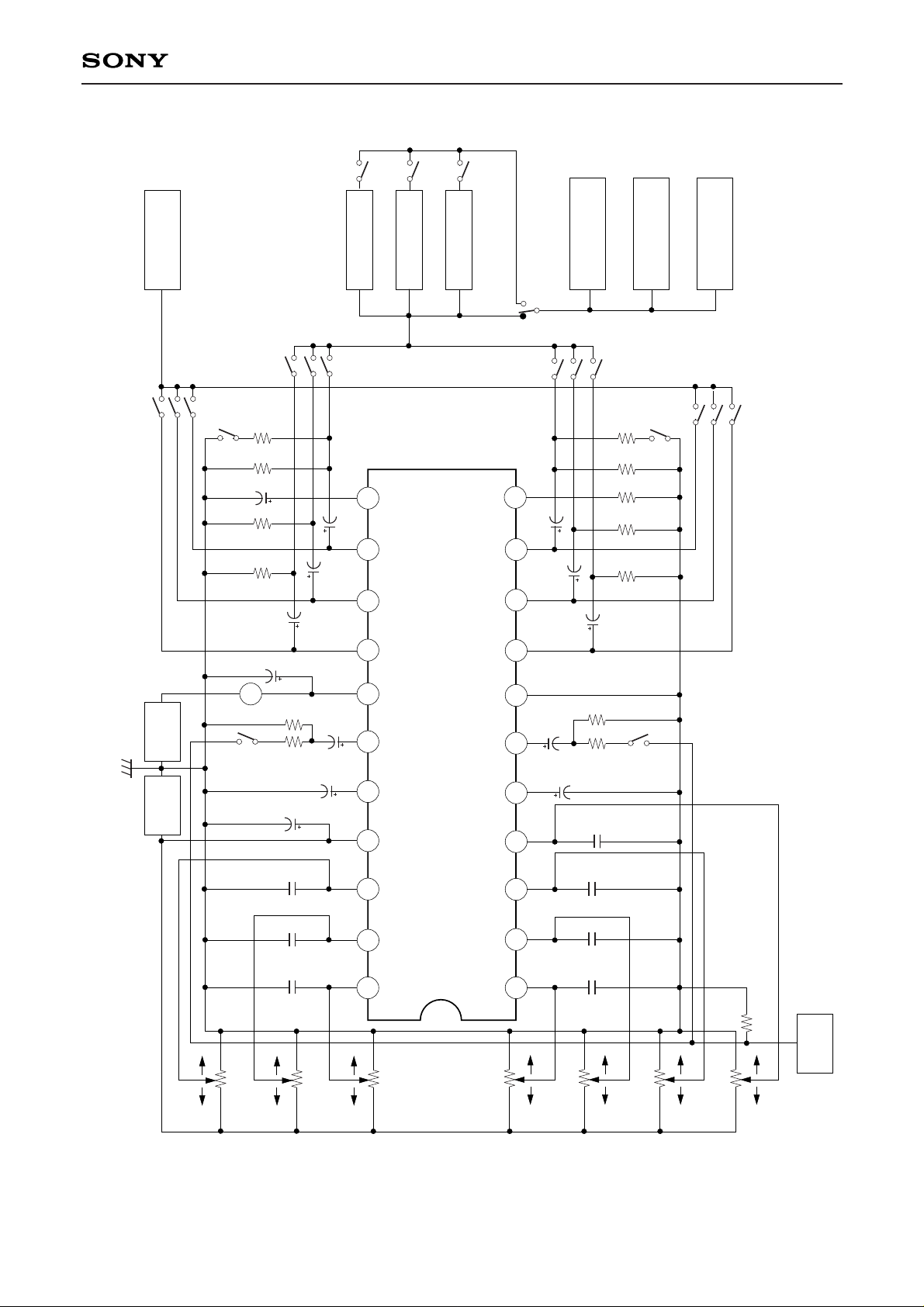
Electrical Characteristics Test Circuit
1 2 3 4 5 6 7 9 10
11
1213141617181920
21
22
GND
POWER
SUPPLY
POWER
SUPPLY
DC
VOLTMETER
S10
S16
S20
S15
S14
S9
S8
S4
R20
2k
R16
20k
R14
20k
R12
5.1k
R10
39k
R19
20k
1kHz BPF
S19
S18
DIN AUDIO
“A” WTG
NOISE FILTER
OUT
S17
IN
FILTER
S13
S12
S11
AC
VOLTMETER
DISTORTION
ANALYZER
OSCILLO
–SCOPE
NOTE
1. RESISTOR TOLERANCE
2. CAPACITOR TOLERANCE
COUPLING CAPACITPR
∗±5%
±1%
∗±5%
±2%
±10%
R21
2k
R18
20k
R17
160k
R15
20k
R13
20k
S3
S7
S6
S5
C18
4.7µ/25V
C19
4.7µ/25V
C16
4.7µ/25V
C11
4.7µ/
25V
C17
4.7µ/25V
C14
4.7µ/25V
C15
4.7µ/25V
8
15
∗
C20
47µ/
25V
∗
C13
100µ/
25V
∗
C10
4.7µ/
25V
∗
C8
100µ/
25V
∗
C6
1000p
∗
C4
1000p
∗
C2
1000p
∗
C1
1000p
∗
C3
1000p
∗
C5
1000p
∗
C7
1000p
∗
C9
4.7µ/
25V
C12
4.7µ/
25V
A
S2
BOOST CUT
BOOST CUT
BOOST CUT
BOOST CUT
BOOST CUT
CH2 CH1
MAX MIN
R7
50k
R6
50k
R5
50k
R4
50k
R3
50k
R2
50k
R1
50k
R8
620
AUDIO
SG
R9
39k
R11
5.1k
S1
CXA1352AS
400Hz
100Hz
BAL
VOL
1kHz
4kHz
10kHz
DV
CC
DC1
IN1
GND
L OUT1
F OUT1
OUT1
ISET
DC2
IN2
V
CC
L OUT2
F OUT2
OUT2
VG
Page 7
—7—
CXA1352AS
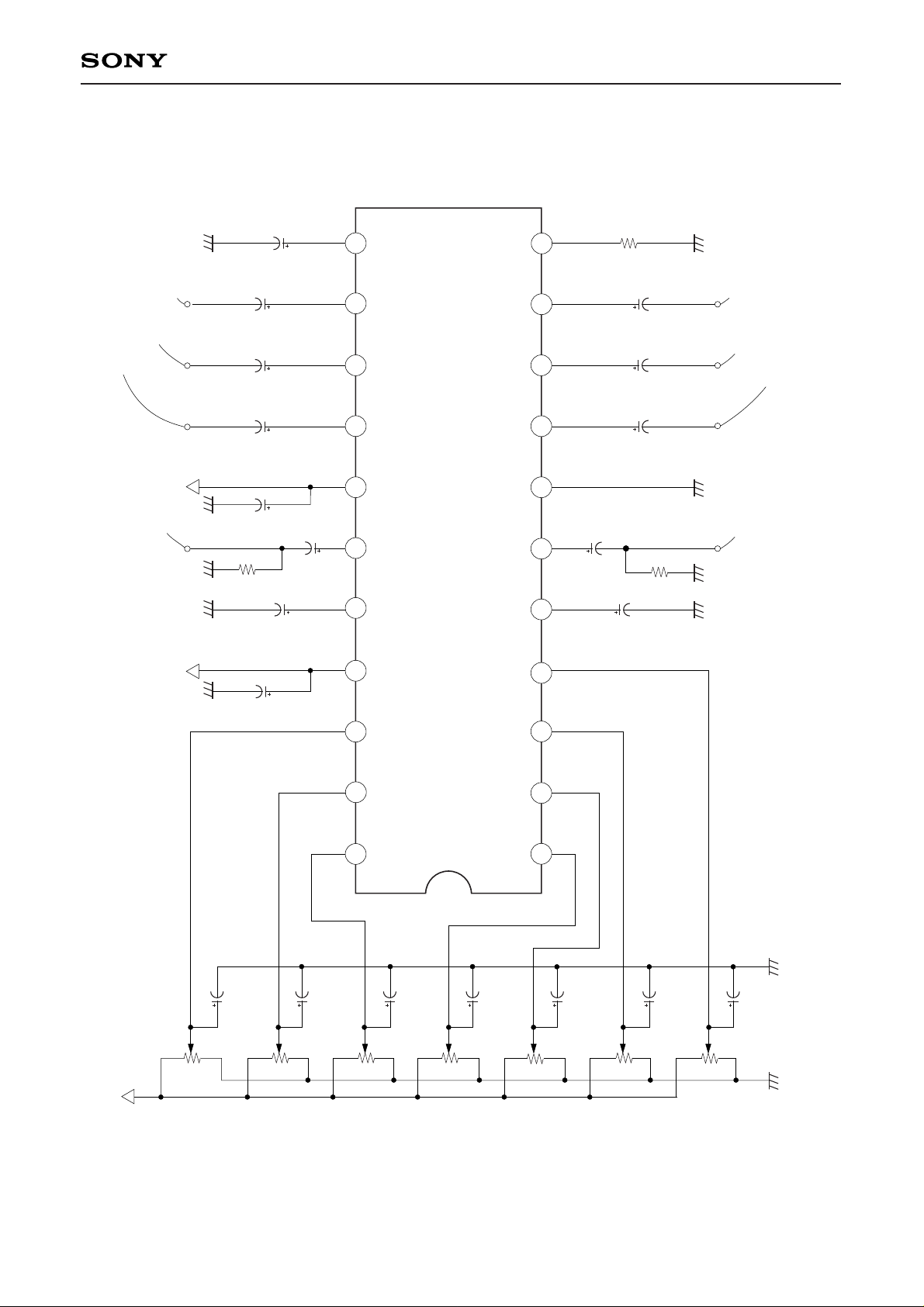
Application Circuit
21
22
121314151617181920
1 2 3 4 5 6 7 8 9
10
11
R7
50k
R6
50k
C7
2.2µ
C6
2.2µ
R5
50k
C5
2.2µ
R4
50k
C4
2.2µ
R3
50k
C3
2.2µ
R2
50k
C2
2.2µ
R1
50k
C1
2.2µ
C9
4.7µ
C11
4.7µ
C14
2.2µ
C16
2.2µ
C18
2.2µ
R10
160k
R8
5.1k
GND
GNDGND
GND GND
V
CC
GND
Signal input
Signal input
To line amplifier
To line amplifier
To power amplifier
To power amplifier
For spectrum analyzer display or
recording through graphic equalizer
For spectrum analyzer display or
recording through graphic equalizer
CXA1352AS
DVCC
DVCC
GND GND GND GND GND
C8
220µ
C10
4.7µ
C12
4.7µ
C13
220µ
C15
2.2µ
C17
2.2µ
C19
2.2µ
C20
4.7µ
R9
5.1k
400Hz
100Hz
BAL
VOL
1kHz
4kHz
10kHz
DV
CC
DC1
IN1
GND
L OUT1
F OUT1
OUT1
ISET
DC2
IN2
V
CC
L OUT2
F OUT2
OUT2
VG
Application circuits shown are typical examples illustrating the operation of the devices. Sony cannot assume responsibility for
any problems arising out of the use of these circuits or for any infringement of third party patent and other right due to same.
Page 8
—8—
CXA1352AS
Description of Operation
1. Graphic equalizer
• Conventional system
Fig. 1.
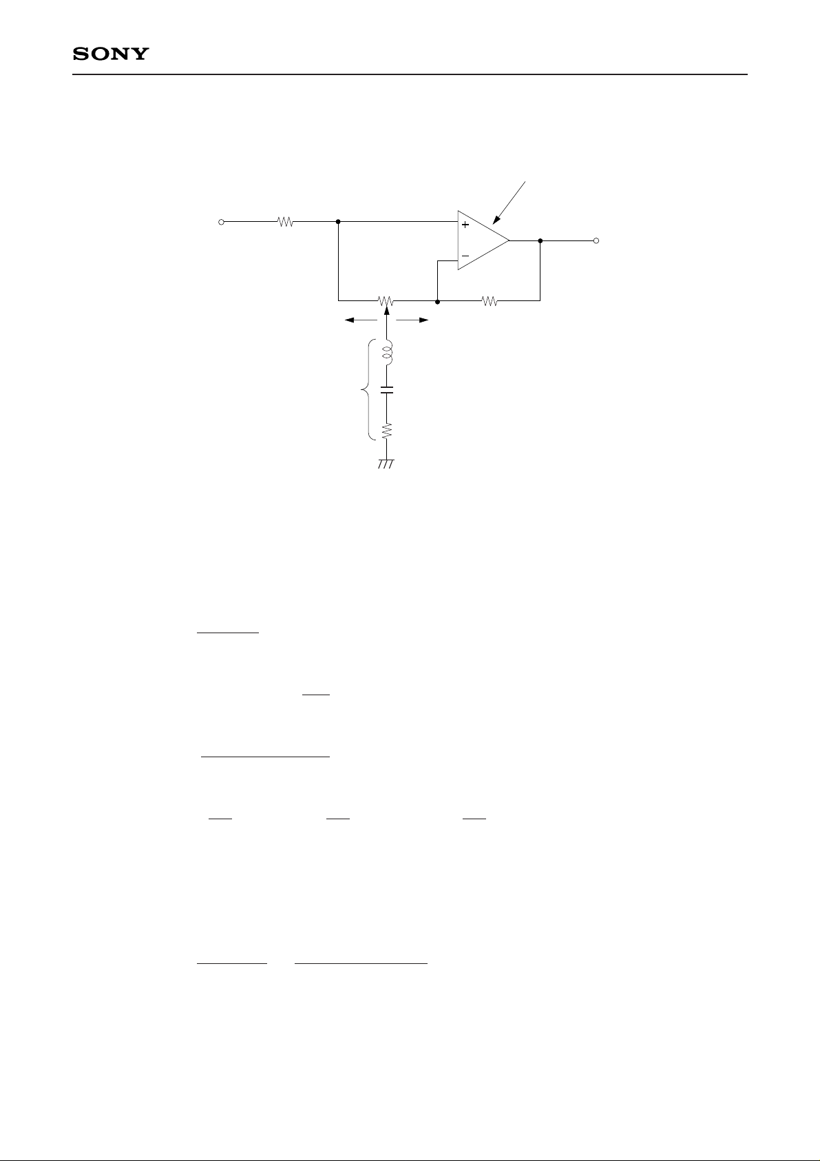
Fig. 1. indicates the conventional graphic equalizer system. This circuit performs boost and cut near “fO”
controlled by the variable volume RV. (“fO” is resonance frequency determined by Z (s) (formed LCR).) The
operation can be seen as follows : When the LCR circuit goes to the far left of RV, a state of graphic
equalizer becomes maximum cut. At that time, assuming transmittance as T (s), we have
T (s) =
Z (s)
Z (s)+ RO
Here as Z (s) = sL+R+
1
sC
Then T (s) =
LCs2+RCs+1
LCs2+ (R+Ro) Cs+1
Defining fo as fO =
ωo
, ωo as ωo =
1
, and Q as Q =
ωoL
,
2π LC R
we can obtain the frequency
characteristics at cut.
Also, when LCR circuit goes to the far right of RV, a state of graphic equalizer becomes maximum boost.
At that time transmittance is :
T (s) =
Z (s) +RO
=
LCs2+ (R+Ro) Cs+1
Z (s) LCs2+RCs+1
Defining fo, ωo and Q as for cut, we can obtain the frequency characteristics at boost.
VI
R1
RV R2
R0=R1=R2
VO
OPERATIONAL AMPLIFIER
BOOSTCUT
L
CZ (s)
R
Page 9

—9—
CXA1352AS
Fig. 2. Indicates frequency characteristics at boost and cut.
Fig. 2.
• CXA1352AS system
Fig. 3.
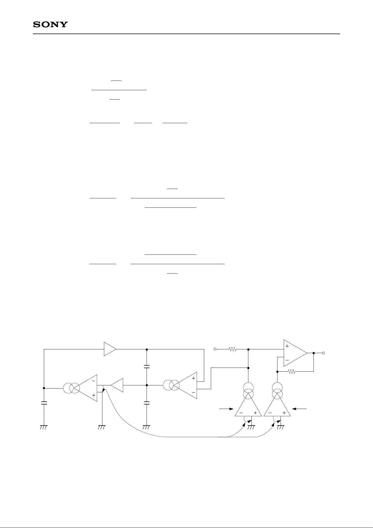
The structure of the graphic equalizer used in this IC is shown on Fig. 3. This circuit performs boost and
cut controlled by 2 transconductance amplifiers that can vary the conversion coefficient through control
currents Ib, and Ic around ωo. (“ωo” is central frequency determined by Band Pass Filter.) Considering
output impedance Z (s) of Gm1, Gm2 we have
Z (s) =
1
H(s) • Gm1
Response (dB)
0dB
Boost
FIat
Cut
f
O=
2π LC
1
Frequency (Hz)
f
O
VI
H(s)=
s2+ s+ωo
2
Q
ωo
s
Q
ωo
H(s)
Ic Ib
Z(s) Z(s)
R
R
Gm1 Gm2
V
O
Operational amplifier
Page 10
—10—
CXA1352AS
Here, using ωo and Q we can express BPF transmittance H (s) as
Z (s) =
Q
s+
1
+
ωo • Q
ωo • Gm1 Gm1 Gm1 • s
This formula shows that this system and the aforementioned LCR circuit have equivalent impedance
characteristics on Z (s).
Then, regarding Gm as the maximum value of Gm1 and Gm2, the operation can be observed as follows.
Maximum cut occurs when Gm1=Gm and Gm2=0. At that time we have transmittance T (s) as
T (s) =
Z (s)
=
Z (s) +R
This is equal to the frequency characteristics of the conventional graphic equalizer at cut.
Also, maximum boost occurs when Gm1=0 and Gm2=Gm. At that time we have transmittance T (s) as
T (s) =
Z (s) +R
=
Z (s)
This is equal to the frequency characteristics of the conventional graphic equalizer at boost.
We can then deduce that, as far as the operation is concerned the graphic equalizer on this IC and the
conventional graphic equalizer are equal, even when the system differs. The merit in using this IC’s system
rests with the fact that monolithic filter technology realizes a graphic equalizer without external parts.
The structure of the actual graphic equalizer, including BPF, is shown on Fig. 4.
Fig. 4
H (s) =
ωo
• s
Q
s2+
ωo
s + ωo
2
Q
s2+
ωo
• s + ωo
2
Q
s2+
(1+R • Gm) • ωo
2
• s+ ωo
2
Q
s2+
ωo
• s + ωo
2
Q
s2+
(1+R • Gm) • ωo
2
• s+ ωo
2
Q
R2
30k
SUM
V
O
Gm4Gm3
Gm1
I CUT I BOOST
GND
GNDGNDGND GND
C2 C1
C3
Gm2
VI
V
I
1
1
R1
30k
Page 11

—11—
CXA1352AS
2. Control through microcomputer possible
Volume, balance and the 100 Hz, 400 Hz, 1 kHz, 4 kHz, 10 kHz boost, cut control respectively are all
executed through DC voltage.
Also, the control voltage range is determined through DVCC (control power supply, independent from VCC)
and is from 0 V to DVCC. Accordingly, the control range can be varied at will, by changing DVCC voltage.
By setting DVCC 5 V, control through the microcomputer becomes possible.
Setting to DVCC=VCC enables usage with single power supply.
3. Pseudo loudness
A loudness function interlocking with volume (VOL) is featured.
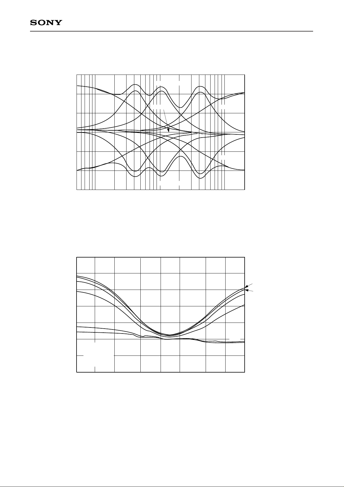
With this IC, to provide a loudness effect, the 100 Hz and 10 kHz graphic equalizer part does not use a
BPF but is composed of a low pass filter (LPF) and a high pass filter (HPF) respectively.
The operation is explained as follows. As VOL drops below the center, the 100 Hz and 10 kHz graphic
equalizer part Ib (See Fig. 3.) gradually increases even if the graphic equalizer control pin (100 Hz and 10
kHz) is flat, boost applies and as a result loudness effect is obtained.
Page 12
—12—
CXA1352AS
Notes on Operation
1. Power supply
DVCC can be used independently from VCC but supply voltage should be
VCC≥DVCC, without fall.
2. Pseudo loudness
As mentioned in the paragraph on Description of Operation, as it is interlocked with VOL, loudness can not
be put OFF.
3. Output pin
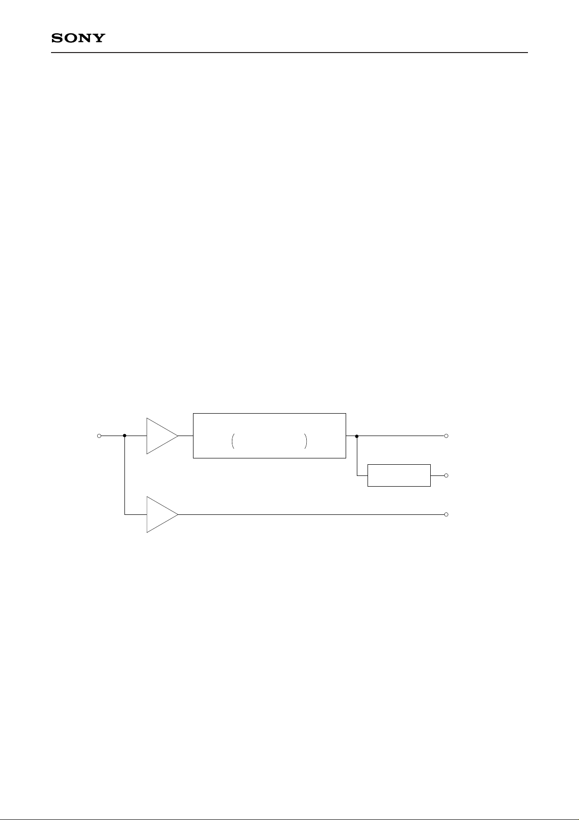
This IC features 2 channels for each of OUT pin, LINE OUT pin and FIX OUT pin.
Usage of the respective output pins is indicated as follows.
• OUT pin
Normally used as the graphic equalizer output.
• LINE OUT pin
A sound from a source that has not passed through the graphic equalizer is only amplified and output
from this pin.
• FIX OUT pin
This pin is useful for REC or spectrum analyzer display after the sound formation at the graphic
equalizer.
The relation between the input and the respective outputs is shown on Fig. 5.
Fig. 5.
4. Reference resistor
To check the central frequency deviation of the graphic equalizer, the control current that determines the
filter time constant is determined by means of an external, not an internal, resistor.
This is the 160 kΩ external resistor connected to ISET pin (Pin 11). Accordingly, for the resistor to be
connected to ISET pin, it is recommended to use a resistor with excellent dispersion and temperature
characteristics.
Also, by varying the value of the resistor connected to ISET pin, the frequency characteristics of the
graphic equalizer can be shifted. By reducing the resistor value the shift moves to the high band and by
increasing the value the shift moves to the low band.
However, 5 elements cannot be shifted independently.
F OUT
–20dBm
L OUT
–5dBm
OUT
–20dBm
(VARIABLE)
VOLUME
IN AMP
–34dBm
IN
14dB
LINE AMP
29dB
GRAPHIC EQUALIZER
GEBPF+GEHPF+
GELPF+SUM AMP
Page 13
—13—
CXA1352AS
Example of Representative Characteristics
15
10
–5
–10
–15
5
0
50 100 200 500 1k 2k 5k 10k 20k
Frequency characterlstlcs
ALL BOOST
ALL FLAT
ALL CUT
BOOST
CUT
RESPONSE(dB)
VCC=8V
DVCC=5V
0dB=–20dBm, 1kHz
VOL : MAX
FREQUENCY(Hz)
–4
8
4
0
50 100 200 500 1k 2k 5k 10k 20k
Loudness characteristics
2.5V
BOOST(dB)
FREQUENCY(Hz)
VCC=8V
DVCC=5V
0dB=at 1kHz
ALL FLAT
VOL=0.0V
1.0V
1.5V
2.0V
5.0V
Page 14
—14—
CXA1352AS
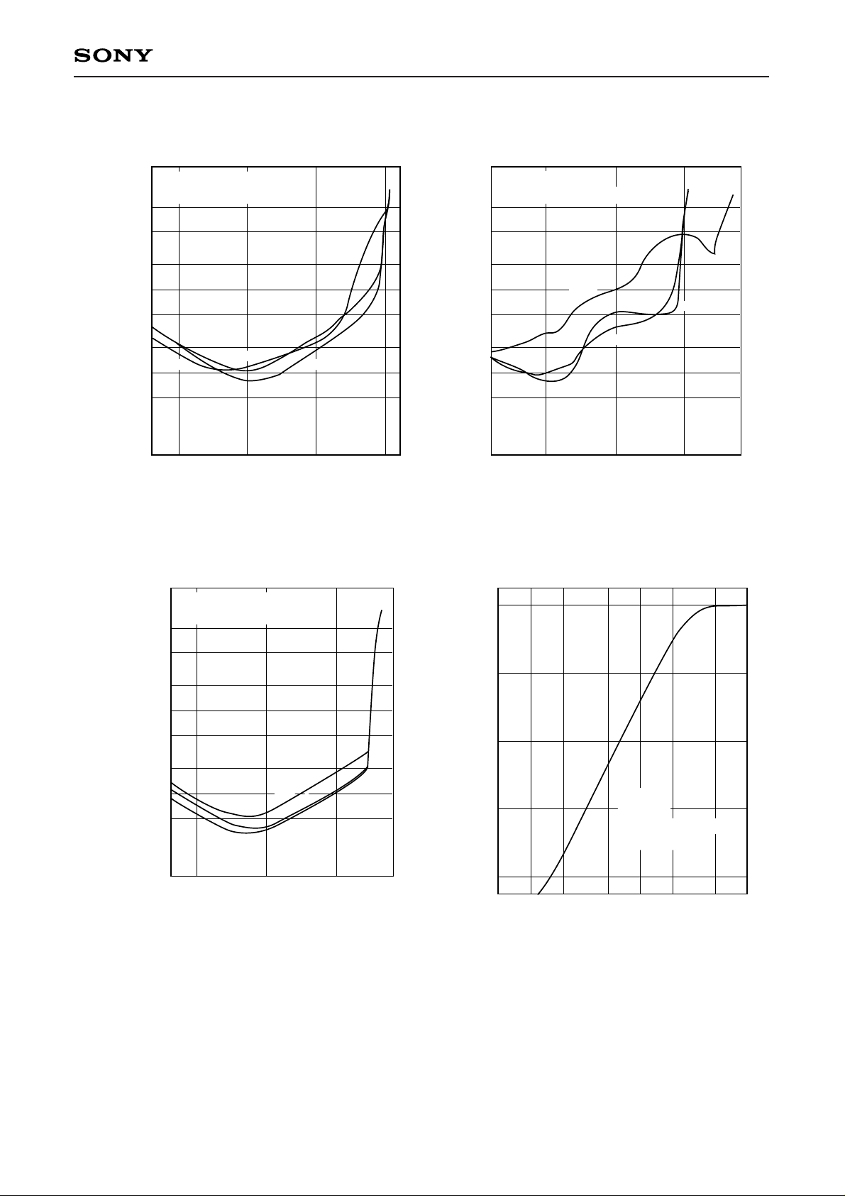
THD-OUT characteristics (ALL FLAT)
VCC=8V, DVCC=5V
0dB=–20dBm, VOL : MAX
10.0
5.0
2.0
1.0
0.5
0.2
0.1
0.05
THD+N (%)
0 10 20
100Hz
10kHz
1kHz
OUT pin output level (dB)
THD-OUT characteristics (ALL BOOST)
VCC=8V, DVCC=5V
0dB=–20dBm‚ VOL : MAX
10.0
5.0
2.0
1.0
0.5
0.2
0.1
0.05
THD+N (%)
0 10 20
100Hz
10kHz
1kHz
OUT pin output level (dB)
THD-OUT characteristics (ALL CUT)
VCC=8V, DVCC=5V
0dB=–20dBm, VOL : MAX
10.0
5.0
2.0
1.0
0.5
0.2
0.1
0.05
THD+N (%)
0 10 20
100Hz
10kHz
1kHz
OUT pin output level (dB)
THD-F OUT characteristics (ALL FLAT)
VCC=8V, DVCC=5V
0dB=–20dBm, VOL : MAX
10.0
5.0
2.0
1.0
0.5
0.2
0.1
0.05
THD+N (%)
0 10 20 30
100Hz
10kHz
1kHz
FIX OUT pin output level (dB)
Page 15
—15—
CXA1352AS
THD-F OUT characteristics (ALL BOOST)
VCC=8V, DVCC=5V
0dB=–20dBm, VOL : MAX
10.0
5.0
2.0
1.0
0.5
0.2
0.1
0.05
THD+N (%)
0 10 20 30
100Hz
10kHz
1kHz
FIX OUT pin output level (dB)
THD-F OUT characteristics (ALL CUT)
VCC=8V, DVCC=5V
0dB=–20dBm, VOL : MAX
10.0
5.0
2.0
1.0
0.5
0.2
0.1
0.05
THD+N (%)
0 10 20
100Hz
10kHz
1kHz
FIX OUT pin output level (dB)
THD-L OUT characteristics
VCC=8V, DVCC=5V
0dB=–6dBm, VOL : MAX
10.0
5.0
2.0
1.0
0.5
0.2
0.1
0.05
THD+N (%)
0 10–10
100Hz
10kHz
1kHz
LINE OUT pin output level (dB)
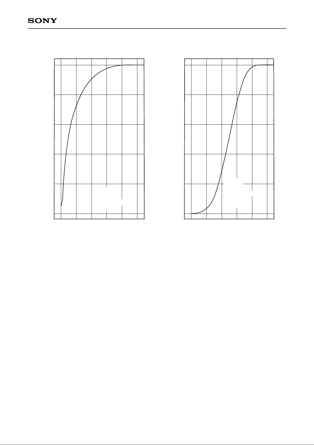
Output voltage vs. Control voltage (VOL)
0
–20
–40
–60
–80
OUT pin output level (dBm)
0.1 0.2 0.5 1 2 5
Control voltage (V)
VCC=8V
DVCC=5V
VIN=–14dBm,1kHz
ALL FLAT
Page 16
—16—
CXA1352AS
Output voltage vs. Control voltage (VOL)
0
–20
–40
–60
–80
–100
OUT pin output level (dBm)
0 1.0 2.0 3.0 4.0 5.0
Control voltage (V)
VCC=8V
DVCC=5V
VIN=–14dBm, 1kHz
ALL FLAT
Output voltage vs. Control voltage (VOL)
100
80
60
40
20
0
OUT pin output level (%)
0 1.0 2.0 3.0 4.0 5.0
Control voltage (V)
VCC=8V
DVCC=5V
VIN=–14dBm, 1kHz
100%=0dBm
ALLFLAT
Page 17

SONY CODE
EIAJ CODE
JEDEC CODE
PACKAGE STRUCTURE
MOLDING COMPOUND
LEAD TREATMENT
LEAD MATERIAL
PACKAGE MASS
EPOXY RESIN
SOLDER PLATING
COPPER ALLOY
22PIN SDIP (PLASTIC)
SDIP-22P-01
SDIP022-P-0300
0.95g
1.778
11
12
1
22
19.2 – 0.1
+ 0.4
7.62
6.4 – 0.1
+ 0.3
0.25 – 0.05
+ 0.1
0° to 15°
0.5 ± 0.1
0.9 – 0.1
+ 0.15
3.25 – 0.2
+ 0.15
0.51 MIN
3.9 – 0.1
+ 0.4
1.All mat surface type.
Two kinds of package surface:
2.All mirror surface type.
Package Outline Unit : mm
CXA1352AS
—17—
 Loading...