

Page 1
CX28394/28395/28398
Quad/x16/Octal—T1/E1/J1 Framers
The CX28394/28395/28398 is a family of multiple framers for T1/E1/J1 and Integrated
Service Digital Network (ISDN) primary rate in terfaces operating at 1.5 44 Mbps or 2 .048
Mbps. All framers are totally independent, and each combines a sophisticated framing
synchronizer and transmit/receive slip buffers. Operations are controlled through a
series of memory-mapped registers accessible via a parallel microprocessor port.
Extensive register support is provided for alarm and error monitoring, signaling
supervision (including ISDN D-channel/SS7 process), per-channel trunk conditioning,
and Facility Data Link (FDL) maintenance. A flexible serial Time Division Multiplexed
(TDM) system interface that supports bus rates from 1.536 to 8.192 MHz is featured.
Extensive test and diagnostic functions include a full set of loopbacks, Pseudo Random
Bit Sequence (PRBS) test pattern generation, Bit Error Rate (BER) meter, and forced
error insertion.
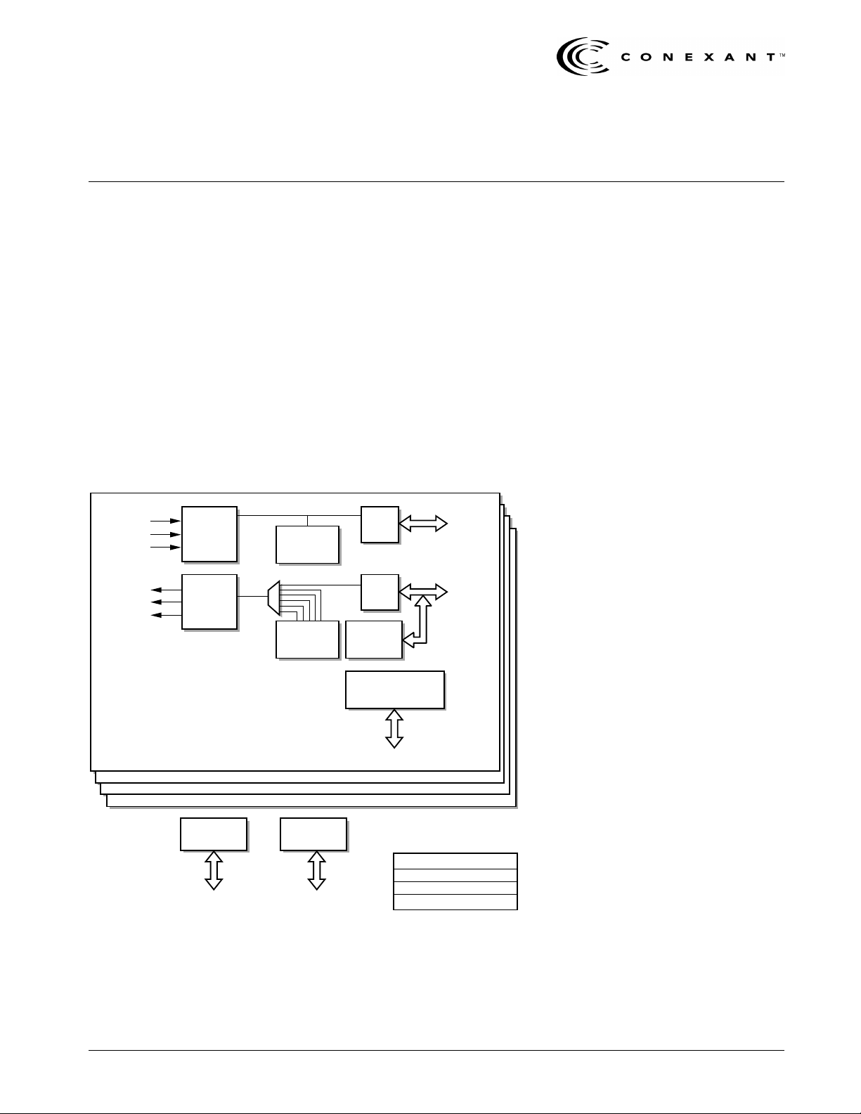
Functional Block Diagram
Receive
Dual Rail or
NRZ
Receive
Dual Rail or
NRZ
Framer #1
.
.
.
Framer #N
* CX28394 and CX28398 only.
Decode
Encode
Test Port
ZCS*
ZCS*
JTAG
T1/E1
Receive
Framer
Overhead
Insertion
Control/Status
Registers
Motorola/Intel
Processor Bus
RX
Slip
Buffer
TX
Slip
Buffer
T1/E1
Transmit
Framer
Data Link Controllers
DL1+DL2
External Data Link
DL3*
CX28394 - 4 Frames
CX28398 - 8 Frames
CX28395 - 16 Frames
Receive
System
Bus
Transmit
System
Bus
Framer #N
8394-8-5_019
Distinguishing Features
• Up to 16 T1/E1/J1 Framers i n one
package
• Extensive support of variou s
protocols
• T1: SF, ESF, SLC
TTC JT(J1)
• E1: PCM-30, G.704, G.706, G.732,
ISDN primary rate (ETS300 011,
INS 500)
• Extracts and inserts signaling bits
• Dual HDLC controllers per framer for
data link and LAPD/SS7 signaling
• Two-fr ame tran smit an d recei ve PCM
slip buffers
• Separate or multiplexed system bus
interfaces
• Parallel 8-bit microprocessor port
supports Intel or Motorola buses
• BERT generation and counting
• B8ZS/HDB3/Bit 7 zero suppression
(CX28394 and CX28398 only)
• Operates from a single +3.3 V dc
± 5% power supply
• Low-power CM OS tec h no lo gy
Applications
• Multiline T1/E1 Channel Service
Unit/Data Service Unit (CSU/DSU)
• Digital Access Cross-Connect
System (DACS)
• T1/E1 Multiple xe r (MUX )
• PBXs and PCM channel bank
• ISDN Primary Rate Access (PRA)
• Frame Relay Switches and Access
Devices (FRADS)
• SONET/SDH add/drop multiplexers
• T3/E3 channelized access
concentrators
®
96, T1DM,
Data Sheet 100054E
June 2000
Page 2
CX28398EVM—Evaluation Module, Octal T1/E1 ISDN PRI Board
T1 or E1 Connection at DSX Levels
Quad T1/E1 LIU (CX28380) Quad T1/E1 LIU (CX28380)
Address
Bus
Microprocessor
Data
Bus
12
8
CX28398 (Octal T1/E1 Framer)
Local PCM Highway (i.e., 2 @ 8192 kbps)
8394-8-5_012
© 1999, 2000, Conexant Systems, Inc.
All Rights Reserved.
Information in this document is provided in connection with Conexant Systems, Inc. (“Conexant”) products. These materials are
provided by Conexant as a service to its customers and may be used for informational purposes only. Conexant assumes no
responsibility for errors or omissions in these materials. Conexant may make changes to specifications and product descript ion s at
any time, without notice. Conexant makes no commitment to update the information and shall have no responsibility whatsoever for
conflicts or incompatibilities arising from future changes to its specifications and product descriptions.
No license, express or implied, by estoppel or otherwise, to any intellectual property rights is granted by this document. Except as
provided in Conexant’s Terms and Conditions of Sale for such products, Conexant assumes no liability whatsoever.
THESE MATERIALS ARE PROVIDED “AS IS” WITHOUT WARRANTYOF ANY KIND, EITHER EXPRESS OR IMPLIED, RELATING
TO SALE AND/OR USE OF CONEXANT PRODUCTS INCLUDING LIABILITY OR WARRANTIES RELATING TO FITNESS FOR A
PARTICULARPURPOSE, CONSEQUENTIAL OR INCIDENTAL DAMAGES,MERCHANTABILITY, OR INFRINGEMENT OF ANY
PATENT, COPYRIGHT OR OTHER INTELLECTUAL PROPERTYRIGHT. CONEXANT FURTHER DOES NOT WARRANT THE
ACCURACY OR COMPLETENESS OF THE INFORMATION, TEXT, GRAPHICS OR OTHER ITEMS CONTAINED WITHIN THESE
MATERIALS. CONEXANT SHALL NOT BE LIABLE FOR ANY SPECIAL, INDIRECT, INCIDENTAL, OR CONSEQUENTIAL
DAMAGES,INCLUDING WITHOUT LIMITATION, LOST REVENUES OR LOST PROFITS, WHICH MAYRESULT FROM THE USE
OF THESE MATERIALS.
Conexant products ar e not intended for use in medical, lifesaving or life sustaining applications. Conexant customers using or selling
Conexant products for use in such applications do so at their own risk and agree to fully indemnify Conexant for any damages
resulting from such improper use o r sale.
The following are trademarks of Conexant Systems, Inc.: Conexant™, the Conexant C symbol, and “What’s Next in Communications
Te chnologies”™. Product names or services listed in this publication are for identification purposes only, and may be trademark s of
third parties. Third-par ty brands and names are the property of their respective owners.
For additional disclaimer information, please consult Conexant’s Legal Information posted at www.conexant.com,whichis
incorporated by reference.
Reader Response: Conexant strives to produce quality documentation and welcomes your feedback. Please send comments and
suggestions to tech.pubs@conexant.com. For tec hnical questions, contact your local Conexant sales office or field applicat ions
engineer.
100054E Conexant
Page 3
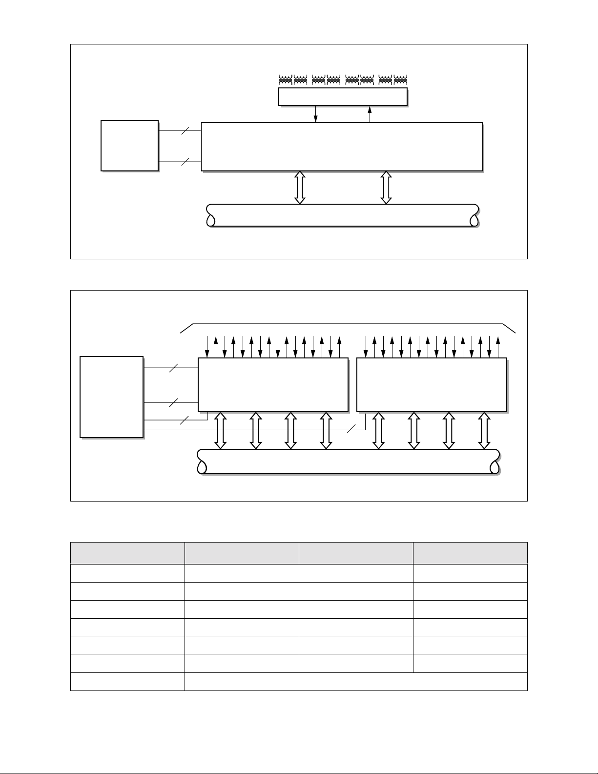
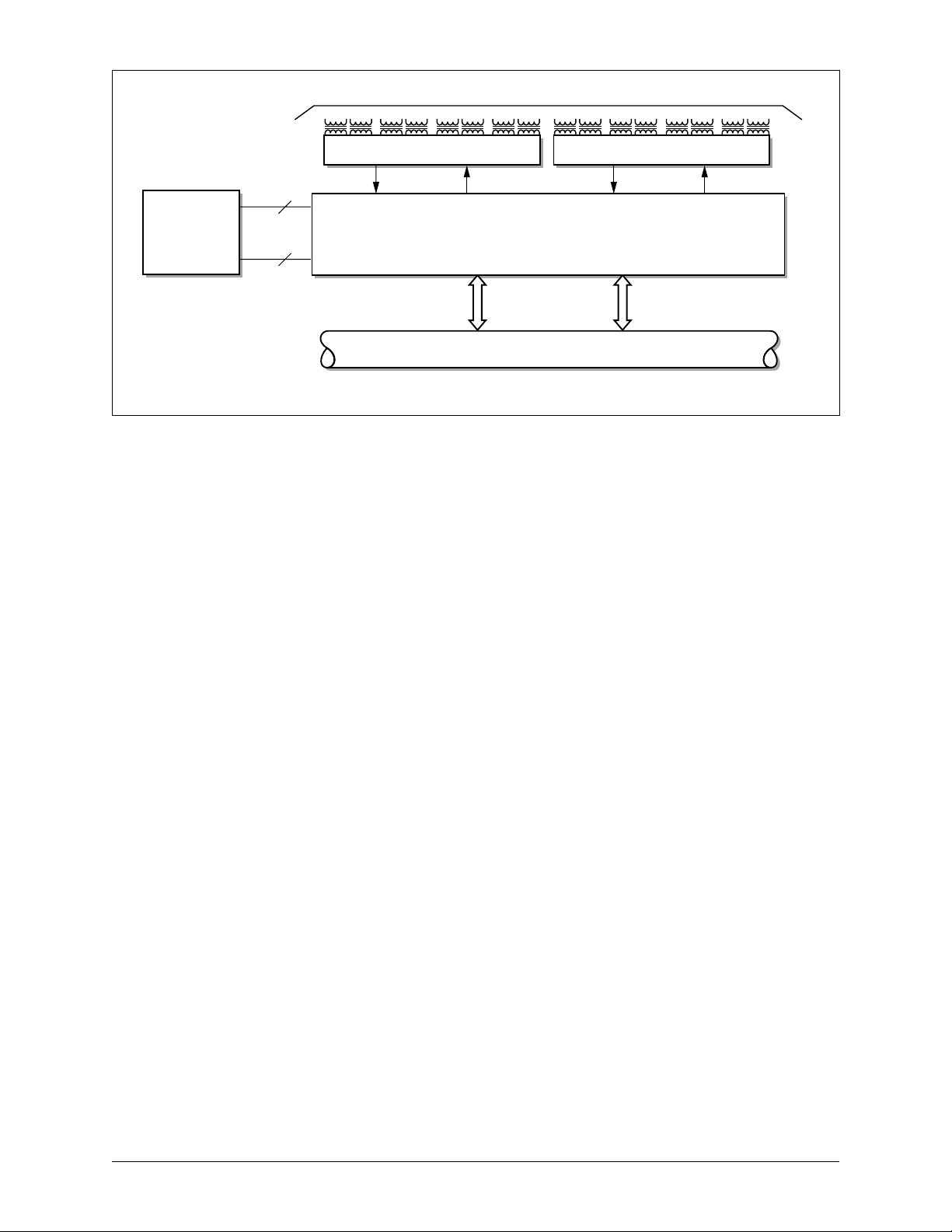
Typical Quad T1/E1 Application
Address
Bus
Microprocessor
Data
Bus
Typical x16 T1/E1 Application
12
T1 or E1 Connection at DSX Levels
CX28380 (Quad LIU)
CX28394 (Octal T1/E1 Framer)
8
Local PCM Highway (8192 kbps)
8394-8-5_015
T1 or E1 Line Interfaces, SONET/SDH Mapper or M13/E13 Mux
Address
Bus
Microprocessor
Data
Bus
Selects
12
8
2
Chip
CX28395 ( x16 T1/E1 Framer)
Local PCM Highways 32 at 1536 kbps to 8 at 8192 kbps)
CX28395 ( x16 T1/E1 Framer)
2
Ordering Information
Model Number Number of Framers Package Operating Temperature
CX28394-22 4 128-pin TQFP –40 to 85 °C
CX28398-22 8 208-pin PQFP –40 to 85 °C
CX28398-23 8 272-pin B G A –40 to 85 °C
CX28395-19 16 318-pin BGA –40 to 85 °C
8394-8-5_014
CX28395-18 16 318-pin BGA 0 to 70 °C
CX28398-24 8 208-pin CABGA –40 to 85 °C
BT00-D660-00 1 CX28398/CX283 80 Ev a lu a t io n Mod ule
100054E Conexant
Page 4

Detailed Feature Summary
Frame Alignm ent
• Framed formats:
– Independent transm it and receive
framing modes
– T1: FT/SF/ESF/SLC/T1DM/TTC-JT(J1)
– E1: FAS/MFAS/FAS+CAS/MFAS+CAS
• Maximum Average Reframe Time
(MART) less than 50 ms
• Transmitter alignment modes:
– Align to system bus data
– Align to system bus sync
– Align to buffer data (embedded
framing)
• Unframed mode
Signaling
• T1: 2-, 4-, or 16-state robbed bit
ABCD signaling
• E1: Channel Associated Signaling
(CAS)
• Common Chann el Si gn a lin g (CCS) in
any time slot
• Per-channel receive signaling stack
• Signaling state change interrupt
• Automatic and manual signaling
freeze
• Debounce signaling (2-bit
integration)
• UNICODE detection
• Signaling reinsertion on PCM system
bus
• Separat e I /O fo r sys te m bu s s ign al in g
• Per-channel tr ansparent
Loopbacks
• Remote loop ba c k toward line
– Retains BPV transparency
(CX28394 and CX28398 only)
• Payload loopback
• Per-channel D S0 remote loopback
• Local loopback towards system
– Framer digital loopback
– Per-channel DS0 local loopback
• Inband loop ba c k co d e dete c t io n/
generation
• Simultaneous local and remote line
loopbacks
Processor Interface
• Parallel 8-bit bu s
• Data strobes (Motorola) or address
latch enable (Intel)
• Multiplexed or non-multiplexed
address/data bus
• Synchronous or asynchronous
data transfers
• Open drain interru pt ou tput with
maskable sources
Out-of-Service Testing
and Maintenance
• Pseudo-Random Bit Sequence
(PRBS):
– Independent transmit and receive
11
–2
; 215; 220; 223 patterns
– Framed or unframe d mode
– Optional 7/14 zero limit
– Bit Error Counter (BERR)
• Single error insertion:
– PRBS error
– Framing error
– CRC error
– BPV/LCV error (C X28394 and
CX28398 only)
– COFA error
System Bus Interface (SBI)
• System bus data rates :
– 1536 kbps (T1 without F-bits)
– 1544 kbps (T1)
– 2048 kbps (E1)
– 4096 kbps (2E1)
– 8192 kbps (4E1)
• Clock operation at 1x or 2x data rate
• Selectable I/O clock edges
• Master, slave, or mixed bus timi ng
• Bit and time slot frame sync offsets
• DS0 drop/insert indicators for
external mux
• Embedded T1 framing transport
per G.802
• Receive and transmit slip buffers
– Bypass, 2-frame, or 64-bit depth
– Slip detection with directi onal
status
– Slip buffer phase status
– Per-channel idle code insertion
– Processor accessible data buffers
• Direct connection to upper layer
devices:
– Link layer: Bt8474
– ATM layer: CN8228
• Direct connection to physical line
interface
– CX28380
• Supported system bus formats:
– ATT Concentration Highway
Interface (CHI)
– Multi-Vendor Integration Protocol
(MVIP)
–Mitel ST-bus
• Separate or internally multiplexed
bus modes
In-Service
Performance Monitoring
• One-second timer I/O to synchronize
reporting
• Receive error detectors with
accumulators:
– Bipolar/Line Code Violations
(LCV) (CX28394 and CX28398
only)
– Excessive Zeros (EXZ)
– Loss of Frame (RLOF)
– Framing Errors (FERR)
– CRC Errors (CERR)
– Far End Block Errors (FEBE)
– Severely Errored Frames (SEF)
– Change of Frame Alignment
(COFA)
• Transmit error detectors:
– Loss of Frame (TLOF)
– Framing Errors (TFERR)
– Multiframe Errors (TMERR)
– CRC Errors (TCERR)
– Loss of Transmit Clock (TL OC )
• Receive alarm detectors:
– Alarm Indication Signal (AIS)
– Loss of Signal (RLOS)
– RAI/Yellow Alarm (YEL)
– Multiframe Yellow (MYEL)
– Lost Frame Alignment (FRED )
– Lost Multiframe Alignment
(MRED)
– Carrier Failure Alarm (CFA) with
8:1 dual slope integrat ion
• Controlled Frame Slip (RFS LIP)
Uncontrolled Frame Slip (RUSLI P)
• Automatic and on-de m and transmit
alarms:
– AIS following RLOS and/or TLOC
– Automatic AIS clock switching
– YEL following FRED
– YEL following 100ms reframe
timeout
– MYEL followin g MRE D
– FEBE followin g C ER R
100054E Conexant
Page 5

Data Links
• Two full-featured data link controllers
(DL1 and DL2):
– 64-octet transmit and receive
FIFOs
– HDLC Message Oriented Protoc ol
(MOP)
– Unformatted data transfer
– Unformatted circular buffer
– End of message/buffer interrupt
– Near full/empty interrupts at
selected depth
• Access any bit combination in any
time slot:
– ISDN D-channels at 16, 32, or 64
kbps
– National/spare bits (SA- bits) in 4
kbps increments
– CCS/SS7
– T1DM R-bits
• Access T1 F-bits in even, odd , or all
frames:
– Automatic Performance Report
Message (PRM) generator
– ESF Facility Data Link (FDL)
– Unformatted SLC-96 overhead
– Bit-Oriented Protocol (BOP)
priority codeword generation and
detection
• Separate I/O for external data link
(DL3) on CX2839 4 and CX28398
devices
100054E Conexant
Page 6

100054E Conexant
Page 7

Table of Contents
List of Figures . . . . . . . . . . . . . . . . . . . . . . . . . . . . . . . . . . . . . . . . . . . . . . . . . . . . . . . . . . . . . . . . . . . . . . . . xv
List of Tables . . . . . . . . . . . . . . . . . . . . . . . . . . . . . . . . . . . . . . . . . . . . . . . . . . . . . . . . . . . . . . . . . . . . . . . . . xvii
1.0 Product Description. . . . . . . . . . . . . . . . . . . . . . . . . . . . . . . . . . . . . . . . . . . . . . . . . . . . . . . . . . . . . 1-1
1.1 Overview. . . . . . . . . . . . . . . . . . . . . . . . . . . . . . . . . . . . . . . . . . . . . . . . . . . . . . . . . . . . . . . . . . 1-1
1.1.1 External Datalink . . . . . . . . . . . . . . . . . . . . . . . . . . . . . . . . . . . . . . . . . . . . . . . . . . . . . . 1-1
1.1.2 RINDO/TINDO . . . . . . . . . . . . . . . . . . . . . . . . . . . . . . . . . . . . . . . . . . . . . . . . . . . . . . . . 1-1
1.1.3 LIU Serial Port . . . . . . . . . . . . . . . . . . . . . . . . . . . . . . . . . . . . . . . . . . . . . . . . . . . . . . . . 1-2
1.1.4 Transmit/Receive Line Interface . . . . . . . . . . . . . . . . . . . . . . . . . . . . . . . . . . . . . . . . . . . 1-2
1.2 Pin Assignments. . . . . . . . . . . . . . . . . . . . . . . . . . . . . . . . . . . . . . . . . . . . . . . . . . . . . . . . . . . . 1-3
2.0 Circuit Description. . . . . . . . . . . . . . . . . . . . . . . . . . . . . . . . . . . . . . . . . . . . . . . . . . . . . . . . . . . . . . 2-1
2.1 Functional Block Diagram. . . . . . . . . . . . . . . . . . . . . . . . . . . . . . . . . . . . . . . . . . . . . . . . . . . . . 2-1
2.2 Receiver . . . . . . . . . . . . . . . . . . . . . . . . . . . . . . . . . . . . . . . . . . . . . . . . . . . . . . . . . . . . . . . . . . 2-4
2.2.1 ZCS Decoder . . . . . . . . . . . . . . . . . . . . . . . . . . . . . . . . . . . . . . . . . . . . . . . . . . . . . . . . . 2-4
2.2.2 In-Band Loopback Code Detection . . . . . . . . . . . . . . . . . . . . . . . . . . . . . . . . . . . . . . . . . 2-5
2.2.3 Error Count ers . . . . . . . . . . . . . . . . . . . . . . . . . . . . . . . . . . . . . . . . . . . . . . . . . . . . . . . . 2-5
2.2.3.1 Frame Bit Err or Counter. . . . . . . . . . . . . . . . . . . . . . . . . . . . . . . . . . . . . . . . . 2-6
2.2.3.2 CRC Error Counter . . . . . . . . . . . . . . . . . . . . . . . . . . . . . . . . . . . . . . . . . . . . 2-6
2.2.3.3 LCV Error Counter. . . . . . . . . . . . . . . . . . . . . . . . . . . . . . . . . . . . . . . . . . . . . 2-6
2.2.3.4 FEBE Counter . . . . . . . . . . . . . . . . . . . . . . . . . . . . . . . . . . . . . . . . . . . . . . . . 2-6
2.2.4 Error Monito r. . . . . . . . . . . . . . . . . . . . . . . . . . . . . . . . . . . . . . . . . . . . . . . . . . . . . . . . . 2-6
2.2.4.1 Frame Bit Error . . . . . . . . . . . . . . . . . . . . . . . . . . . . . . . . . . . . . . . . . . . . . . . 2-6
2.2.4.2 MFAS Error. . . . . . . . . . . . . . . . . . . . . . . . . . . . . . . . . . . . . . . . . . . . . . . . . . 2-7
2.2.4.3 CAS Error . . . . . . . . . . . . . . . . . . . . . . . . . . . . . . . . . . . . . . . . . . . . . . . . . . . 2-7
2.2.4.4 CRC Error . . . . . . . . . . . . . . . . . . . . . . . . . . . . . . . . . . . . . . . . . . . . . . . . . . . 2-7
2.2.4.5 Pulse Density Violation . . . . . . . . . . . . . . . . . . . . . . . . . . . . . . . . . . . . . . . . . 2-7
100054E Conexant vii
Page 8

Table of Contents CX28394/28395/28398
Quad/x16/Octal—T1/E1/J1 Framers
2.2.5 Alarm Monitor . . . . . . . . . . . . . . . . . . . . . . . . . . . . . . . . . . . . . . . . . . . . . . . . . . . . . . . . 2-7
2.2.5.1 Loss of Frame. . . . . . . . . . . . . . . . . . . . . . . . . . . . . . . . . . . . . . . . . . . . . . . . 2-8
2.2.5.2 Loss of Signal. . . . . . . . . . . . . . . . . . . . . . . . . . . . . . . . . . . . . . . . . . . . . . . . 2-8
2.2.5.3 Receive Analog Loss of Signal. . . . . . . . . . . . . . . . . . . . . . . . . . . . . . . . . . . . 2-8
2.2.5.4 Alarm Indication Signa l . . . . . . . . . . . . . . . . . . . . . . . . . . . . . . . . . . . . . . . . . 2-8
2.2.5.5 Yellow Alarm. . . . . . . . . . . . . . . . . . . . . . . . . . . . . . . . . . . . . . . . . . . . . . . . . 2-8
2.2.5.6 Multiframe YEL. . . . . . . . . . . . . . . . . . . . . . . . . . . . . . . . . . . . . . . . . . . . . . . 2 -9
2.2.5.7 Severely Errored Frame. . . . . . . . . . . . . . . . . . . . . . . . . . . . . . . . . . . . . . . . . 2-9
2.2.5.8 Change of Frame Alignment. . . . . . . . . . . . . . . . . . . . . . . . . . . . . . . . . . . . . . 2-9
2.2.5.9 Receive Multiframe AIS. . . . . . . . . . . . . . . . . . . . . . . . . . . . . . . . . . . . . . . . . 2-9
2.2.6 Test Pattern Receiver . . . . . . . . . . . . . . . . . . . . . . . . . . . . . . . . . . . . . . . . . . . . . . . . . . . 2-9
2.2.7 Receive Framing. . . . . . . . . . . . . . . . . . . . . . . . . . . . . . . . . . . . . . . . . . . . . . . . . . . . . . 2-10
2.2.8 External Receive Data Link (CX28394 and CX28398 Only) . . . . . . . . . . . . . . . . . . . . . . . 2-15
2.2.9 Sa-Byte Receive Buffers . . . . . . . . . . . . . . . . . . . . . . . . . . . . . . . . . . . . . . . . . . . . . . . . 2-15
2.2.10 Receive Data Link. . . . . . . . . . . . . . . . . . . . . . . . . . . . . . . . . . . . . . . . . . . . . . . . . . . . . 2-16
2.2.10.1 Data Link C ontrollers. . . . . . . . . . . . . . . . . . . . . . . . . . . . . . . . . . . . . . . . . . 2-16
2.2.10.2 RBOP Receiver . . . . . . . . . . . . . . . . . . . . . . . . . . . . . . . . . . . . . . . . . . . . . . 2-20
2.3 System Bus. . . . . . . . . . . . . . . . . . . . . . . . . . . . . . . . . . . . . . . . . . . . . . . . . . . . . . . . . . . . . . . 2-21
2.3.1 Non-Multiplexed Mode. . . . . . . . . . . . . . . . . . . . . . . . . . . . . . . . . . . . . . . . . . . . . . . . . 2-21
2.3.2 Externally Multiplexed Mode. . . . . . . . . . . . . . . . . . . . . . . . . . . . . . . . . . . . . . . . . . . . . 2-22
2.3.3 Internally Multiplexed Mode . . . . . . . . . . . . . . . . . . . . . . . . . . . . . . . . . . . . . . . . . . . . . 2-23
2.3.4 Receive System Bus. . . . . . . . . . . . . . . . . . . . . . . . . . . . . . . . . . . . . . . . . . . . . . . . . . . 2-24
2.3.4.1 Timebase . . . . . . . . . . . . . . . . . . . . . . . . . . . . . . . . . . . . . . . . . . . . . . . . . . 2-28
2.3.4.2 Slip Buffer . . . . . . . . . . . . . . . . . . . . . . . . . . . . . . . . . . . . . . . . . . . . . . . . . 2-28
2.3.4.3 Signaling Buffer . . . . . . . . . . . . . . . . . . . . . . . . . . . . . . . . . . . . . . . . . . . . . 2-30
2.3.4.4 Signaling Stack . . . . . . . . . . . . . . . . . . . . . . . . . . . . . . . . . . . . . . . . . . . . . . 2-31
2.3.4.5 Embedded Framing. . . . . . . . . . . . . . . . . . . . . . . . . . . . . . . . . . . . . . . . . . . 2-31
2.3.5 Transmit System Bus . . . . . . . . . . . . . . . . . . . . . . . . . . . . . . . . . . . . . . . . . . . . . . . . . . 2-32
2.3.5.1 Timebase . . . . . . . . . . . . . . . . . . . . . . . . . . . . . . . . . . . . . . . . . . . . . . . . . . 2-35
2.3.5.2 Slip Buffer . . . . . . . . . . . . . . . . . . . . . . . . . . . . . . . . . . . . . . . . . . . . . . . . . 2-35
2.3.5.3 Signaling Buffer . . . . . . . . . . . . . . . . . . . . . . . . . . . . . . . . . . . . . . . . . . . . . 2-36
2.3.5.4 Transmit Framing . . . . . . . . . . . . . . . . . . . . . . . . . . . . . . . . . . . . . . . . . . . . 2-36
2.3.5.5 Embedded Framing. . . . . . . . . . . . . . . . . . . . . . . . . . . . . . . . . . . . . . . . . . . 2-39
2.4 T ransmitter . . . . . . . . . . . . . . . . . . . . . . . . . . . . . . . . . . . . . . . . . . . . . . . . . . . . . . . . . . . . . . . 2-40
2.4.1 External Transmit Data Link (CX28394 and CX28398 Only) . . . . . . . . . . . . . . . . . . . . . . 2-41
2.4.2 Transmit Data Links . . . . . . . . . . . . . . . . . . . . . . . . . . . . . . . . . . . . . . . . . . . . . . . . . . . 2-41
2.4.2.1 Data Link C ontrollers. . . . . . . . . . . . . . . . . . . . . . . . . . . . . . . . . . . . . . . . . . 2-41
2.4.2.2 Circular Buffer. . . . . . . . . . . . . . . . . . . . . . . . . . . . . . . . . . . . . . . . . . . . . . . 2-42
2.4.2.3 Time Slot and Bit Selection . . . . . . . . . . . . . . . . . . . . . . . . . . . . . . . . . . . . . 2-43
2.4.2.4 Transmit Data Link FIFO Buffer . . . . . . . . . . . . . . . . . . . . . . . . . . . . . . . . . . 2-43
2.4.2.5 End of Message . . . . . . . . . . . . . . . . . . . . . . . . . . . . . . . . . . . . . . . . . . . . . 2-43
2.4.2.6 Programmi ng the Data Li nk Controller . . . . . . . . . . . . . . . . . . . . . . . . . . . . . 2-44
2.4.2.7 PRM Genera tor. . . . . . . . . . . . . . . . . . . . . . . . . . . . . . . . . . . . . . . . . . . . . . 2-46
2.4.2.8 TBOP Transceiver . . . . . . . . . . . . . . . . . . . . . . . . . . . . . . . . . . . . . . . . . . . . 2-46
viii Conexant 100054E
Page 9

CX28394/28395/28398 Table of Contents
Quad/x16/Octal—T1/E1/J1 Framers
2.4.3 Sa-Byte Overwrite Buffer . . . . . . . . . . . . . . . . . . . . . . . . . . . . . . . . . . . . . . . . . . . . . . . 2-46
2.4.4 Overhead Pattern Generation . . . . . . . . . . . . . . . . . . . . . . . . . . . . . . . . . . . . . . . . . . . . 2-47
2.4.4.1 Framing Pattern Generation. . . . . . . . . . . . . . . . . . . . . . . . . . . . . . . . . . . . . 2-47
2.4.4.2 Alarm Generation . . . . . . . . . . . . . . . . . . . . . . . . . . . . . . . . . . . . . . . . . . . . 2-47
2.4.4.3 CRC Generation . . . . . . . . . . . . . . . . . . . . . . . . . . . . . . . . . . . . . . . . . . . . . 2-49
2.4.4.4 Far-End Block Erro r Generation . . . . . . . . . . . . . . . . . . . . . . . . . . . . . . . . . . 2-49
2.4.5 Test Pattern Generation . . . . . . . . . . . . . . . . . . . . . . . . . . . . . . . . . . . . . . . . . . . . . . . . 2-50
2.4.6 Transmit Error Insertion . . . . . . . . . . . . . . . . . . . . . . . . . . . . . . . . . . . . . . . . . . . . . . . . 2-50
2.4.7 In-Band Loopback Code Generation . . . . . . . . . . . . . . . . . . . . . . . . . . . . . . . . . . . . . . . 2-51
2.4.8 ZCS Encoder . . . . . . . . . . . . . . . . . . . . . . . . . . . . . . . . . . . . . . . . . . . . . . . . . . . . . . . . 2-51
2.5 Microp rocessor Interface . . . . . . . . . . . . . . . . . . . . . . . . . . . . . . . . . . . . . . . . . . . . . . . . . . . . 2-55
2.5.1 Address/Data Bus. . . . . . . . . . . . . . . . . . . . . . . . . . . . . . . . . . . . . . . . . . . . . . . . . . . . . 2-56
2.5.2 Bus Control Signals . . . . . . . . . . . . . . . . . . . . . . . . . . . . . . . . . . . . . . . . . . . . . . . . . . . 2-56
2.5.3 Interrupt Requests. . . . . . . . . . . . . . . . . . . . . . . . . . . . . . . . . . . . . . . . . . . . . . . . . . . . 2-56
2.5.4 Device Reset . . . . . . . . . . . . . . . . . . . . . . . . . . . . . . . . . . . . . . . . . . . . . . . . . . . . . . . . 2-58
2.6 Loopbacks. . . . . . . . . . . . . . . . . . . . . . . . . . . . . . . . . . . . . . . . . . . . . . . . . . . . . . . . . . . . . . . . 2-59
2.6.1 Remote Line Loopback. . . . . . . . . . . . . . . . . . . . . . . . . . . . . . . . . . . . . . . . . . . . . . . . . 2-59
2.6.2 Remote Payload Loopback. . . . . . . . . . . . . . . . . . . . . . . . . . . . . . . . . . . . . . . . . . . . . . 2-59
2.6.3 Remote Per-Channel Loopback. . . . . . . . . . . . . . . . . . . . . . . . . . . . . . . . . . . . . . . . . . . 2-59
2.6.4 Local Framer Loopback . . . . . . . . . . . . . . . . . . . . . . . . . . . . . . . . . . . . . . . . . . . . . . . . 2-60
2.6.5 Local Per-Channel Loopback. . . . . . . . . . . . . . . . . . . . . . . . . . . . . . . . . . . . . . . . . . . . . 2-60
2.7 Serial Interface. . . . . . . . . . . . . . . . . . . . . . . . . . . . . . . . . . . . . . . . . . . . . . . . . . . . . . . . . . . . 2-61
2.8 Joint Test Access Group . . . . . . . . . . . . . . . . . . . . . . . . . . . . . . . . . . . . . . . . . . . . . . . . . . . . . 2-62
2.8.1 Instructions. . . . . . . . . . . . . . . . . . . . . . . . . . . . . . . . . . . . . . . . . . . . . . . . . . . . . . . . . 2-62
2.8.2 Device Identification Register . . . . . . . . . . . . . . . . . . . . . . . . . . . . . . . . . . . . . . . . . . . . 2-63
3.0 Registers . . . . . . . . . . . . . . . . . . . . . . . . . . . . . . . . . . . . . . . . . . . . . . . . . . . . . . . . . . . . . . . . . . . . . . 3-1
3.1 Address Map. . . . . . . . . . . . . . . . . . . . . . . . . . . . . . . . . . . . . . . . . . . . . . . . . . . . . . . . . . . . . . . 3-1
3.2 Global Control and Status Registers . . . . . . . . . . . . . . . . . . . . . . . . . . . . . . . . . . . . . . . . . . . . . 3-8
000—Device Identification (DID) . . . . . . . . . . . . . . . . . . . . . . . . . . . . . . . . . . . . . . . . . . 3-8
080—Framer Control Register (FCR) . . . . . . . . . . . . . . . . . . . . . . . . . . . . . . . . . . . . . . . 3-8
081—Master Interrupt Request (MIR) . . . . . . . . . . . . . . . . . . . . . . . . . . . . . . . . . . . . . . 3-9
082—Master Interrupt Enable (MIE). . . . . . . . . . . . . . . . . . . . . . . . . . . . . . . . . . . . . . . 3-10
083—Test Configurat i on (TE ST ). . . . . . . . . . . . . . . . . . . . . . . . . . . . . . . . . . . . . . . . . . 3-10
3.3 Primary Control and Status Register. . . . . . . . . . . . . . . . . . . . . . . . . . . . . . . . . . . . . . . . . . . . 3-11
001—Primary Control Register (CR0). . . . . . . . . . . . . . . . . . . . . . . . . . . . . . . . . . . . . . 3-11
3.4 Interrupt Control Regist er . . . . . . . . . . . . . . . . . . . . . . . . . . . . . . . . . . . . . . . . . . . . . . . . . . . . 3-13
003—Interrupt Request Register (IRR). . . . . . . . . . . . . . . . . . . . . . . . . . . . . . . . . . . . . 3-13
100054E Conexant ix
Page 10

Table of Contents CX28394/28395/28398
Quad/x16/Octal—T1/E1/J1 Framers
3.5 Interrupt St at us Registers . . . . . . . . . . . . . . . . . . . . . . . . . . . . . . . . . . . . . . . . . . . . . . . . . . . . 3-15
004—Alarm 1 Interrupt Status (ISR7). . . . . . . . . . . . . . . . . . . . . . . . . . . . . . . . . . . . . . 3-16
005—Alarm 2 Interrupt Status (ISR6). . . . . . . . . . . . . . . . . . . . . . . . . . . . . . . . . . . . . . 3-17
006—Error Interrupt Status (ISR5). . . . . . . . . . . . . . . . . . . . . . . . . . . . . . . . . . . . . . . . 3-18
007—Counter Overflow Interrupt Status (ISR4) . . . . . . . . . . . . . . . . . . . . . . . . . . . . . . 3-19
008—Timer Interrupt Status (ISR3) . . . . . . . . . . . . . . . . . . . . . . . . . . . . . . . . . . . . . . . 3-19
009—Data Link 1 Interrupt Status (ISR2). . . . . . . . . . . . . . . . . . . . . . . . . . . . . . . . . . . 3-20
00A—Data Li nk 2 Interrupt Status (ISR1). . . . . . . . . . . . . . . . . . . . . . . . . . . . . . . . . . . 3-21
00B—Pattern Interrupt Status (ISR 0) . . . . . . . . . . . . . . . . . . . . . . . . . . . . . . . . . . . . . . 3-22
3.6 Interrupt Enable Registers . . . . . . . . . . . . . . . . . . . . . . . . . . . . . . . . . . . . . . . . . . . . . . . . . . . 3-23
00C—Alarm 1 Interrupt Enable Register (IER7). . . . . . . . . . . . . . . . . . . . . . . . . . . . . . . 3-23
00D—Alarm 2 Interrupt Enable Register (IER6). . . . . . . . . . . . . . . . . . . . . . . . . . . . . . . 3-23
00E—Error Interrupt Enable Register (IER5). . . . . . . . . . . . . . . . . . . . . . . . . . . . . . . . . 3-24
00F—Count Overflow Interrupt Enable Register (IER4) . . . . . . . . . . . . . . . . . . . . . . . . . 3-24
010—Timer Interrupt Enable Register (IER3) . . . . . . . . . . . . . . . . . . . . . . . . . . . . . . . . 3-25
011—Data Link 1 Interrupt Enable Register (IER2) . . . . . . . . . . . . . . . . . . . . . . . . . . . . 3-25
012—Data Link 2 Interrupt Enable Register (IER1) . . . . . . . . . . . . . . . . . . . . . . . . . . . . 3-26
013—Pattern Interrupt Enable Register (IER0) . . . . . . . . . . . . . . . . . . . . . . . . . . . . . . . 3-26
3.7 Primary Control and Status Registers . . . . . . . . . . . . . . . . . . . . . . . . . . . . . . . . . . . . . . . . . . . 3-27
014—Loopback Configuration Register (LOOP) . . . . . . . . . . . . . . . . . . . . . . . . . . . . . . 3-27
015—External Data Link Time Slot (DL3_TS) . . . . . . . . . . . . . . . . . . . . . . . . . . . . . . . . 3-28
016—External Data Link Bit (DL3_BIT). . . . . . . . . . . . . . . . . . . . . . . . . . . . . . . . . . . . . 3-29
017—Offline Framer Status (FSTAT). . . . . . . . . . . . . . . . . . . . . . . . . . . . . . . . . . . . . . . 3-29
018—Programmable Input/Output (PIO). . . . . . . . . . . . . . . . . . . . . . . . . . . . . . . . . . . . 3-31
019—Programmable Output Enable (POE) . . . . . . . . . . . . . . . . . . . . . . . . . . . . . . . . . . 3-33
01A—Clock Input Mux (CMU X) . . . . . . . . . . . . . . . . . . . . . . . . . . . . . . . . . . . . . . . . . . 3-34
020—Receive Alarm Configuration (RAC). . . . . . . . . . . . . . . . . . . . . . . . . . . . . . . . . . . 3-34
021—Receive Line Code Status (RSTAT) . . . . . . . . . . . . . . . . . . . . . . . . . . . . . . . . . . . 3-35
3.8 Seri al Inte rface Registers . . . . . . . . . . . . . . . . . . . . . . . . . . . . . . . . . . . . . . . . . . . . . . . . . . . . 3-36
022—Serial Control (SER_CTL) . . . . . . . . . . . . . . . . . . . . . . . . . . . . . . . . . . . . . . . . . . 3-36
023—Serial Data (SER_DAT) . . . . . . . . . . . . . . . . . . . . . . . . . . . . . . . . . . . . . . . . . . . . 3-36
024—Serial Status (SER_STAT) . . . . . . . . . . . . . . . . . . . . . . . . . . . . . . . . . . . . . . . . . . 3-36
025—Serial Configuration (S ER_CONFIG). . . . . . . . . . . . . . . . . . . . . . . . . . . . . . . . . . . 3-37
026—RAM Test . . . . . . . . . . . . . . . . . . . . . . . . . . . . . . . . . . . . . . . . . . . . . . . . . . . . . . 3-37
3.9 Receiver Registers . . . . . . . . . . . . . . . . . . . . . . . . . . . . . . . . . . . . . . . . . . . . . . . . . . . . . . . . . 3-38
040—Receiver Configuration (RCR0) . . . . . . . . . . . . . . . . . . . . . . . . . . . . . . . . . . . . . . 3-38
041—Receive Test Pattern Configuration (RPATT). . . . . . . . . . . . . . . . . . . . . . . . . . . . . 3-39
042—Receive Loopback Code Detector Configuration (RLB) . . . . . . . . . . . . . . . . . . . . . 3-40
043—Loopback Activate Code Pattern (LBA). . . . . . . . . . . . . . . . . . . . . . . . . . . . . . . . . 3-41
044—Loopback Deactivate Code Pattern (LBD). . . . . . . . . . . . . . . . . . . . . . . . . . . . . . . 3-41
045—Receive Alarm Signal Configuration (RALM) . . . . . . . . . . . . . . . . . . . . . . . . . . . . 3-42
046—Alarm/Error/Counter Latch Configuration (LATCH) . . . . . . . . . . . . . . . . . . . . . . . . 3-44
047—Alarm 1 Status (ALM1). . . . . . . . . . . . . . . . . . . . . . . . . . . . . . . . . . . . . . . . . . . . 3-45
048—Alarm 2 Status (ALM2). . . . . . . . . . . . . . . . . . . . . . . . . . . . . . . . . . . . . . . . . . . . 3-47
049—Alarm 3 Status (ALM3). . . . . . . . . . . . . . . . . . . . . . . . . . . . . . . . . . . . . . . . . . . . 3-48
x Conexant 100054E
Page 11

CX28394/28395/28398 Table of Contents
Quad/x16/Octal—T1/E1/J1 Framers
3.10 Performance Monitoring Registers . . . . . . . . . . . . . . . . . . . . . . . . . . . . . . . . . . . . . . . . . . . . . 3-49
050—Framing Bit Error Counter LSB (FERR) . . . . . . . . . . . . . . . . . . . . . . . . . . . . . . . . 3-49
051—Framing Bit Error Counter MSB (FERR). . . . . . . . . . . . . . . . . . . . . . . . . . . . . . . . 3-49
052—CRC Error Co unter LSB (CERR). . . . . . . . . . . . . . . . . . . . . . . . . . . . . . . . . . . . . . 3-49
053—CRC Error Coun ter MSB (CERR) . . . . . . . . . . . . . . . . . . . . . . . . . . . . . . . . . . . . . 3-49
054—Line Code Violation Counter LSB (LCV) . . . . . . . . . . . . . . . . . . . . . . . . . . . . . . . . 3-50
055—Line Code Violati on Counter MSB (LCV) . . . . . . . . . . . . . . . . . . . . . . . . . . . . . . . 3-50
056—Far End Block Error Co unter LSB (FEBE) . . . . . . . . . . . . . . . . . . . . . . . . . . . . . . . 3-50
057—Far End Block Error Counter MSB (FEBE). . . . . . . . . . . . . . . . . . . . . . . . . . . . . . . 3-50
058—PRBS Bit Error Counter LSB (BERR) . . . . . . . . . . . . . . . . . . . . . . . . . . . . . . . . . . 3-50
059—PRBS Bit Error Counter MSB (BERR) . . . . . . . . . . . . . . . . . . . . . . . . . . . . . . . . . 3-51
05A—SEF/FRED/COFA Alarm Counter (AERR). . . . . . . . . . . . . . . . . . . . . . . . . . . . . . . . 3-51
3.11 Receive Sa-Byte Buffers . . . . . . . . . . . . . . . . . . . . . . . . . . . . . . . . . . . . . . . . . . . . . . . . . . . . . 3-52
05B—Receive Sa4 Byte Buffer (RSA4) . . . . . . . . . . . . . . . . . . . . . . . . . . . . . . . . . . . . . 3-52
05C—Receive Sa5 Byte Buffer (RSA5) . . . . . . . . . . . . . . . . . . . . . . . . . . . . . . . . . . . . . 3-52
05D—Receive Sa6 Byte Buffer (RSA6) . . . . . . . . . . . . . . . . . . . . . . . . . . . . . . . . . . . . . 3-53
05E—Receive Sa7 Byte Buffer (RSA7) . . . . . . . . . . . . . . . . . . . . . . . . . . . . . . . . . . . . . 3-53
05F—Receive Sa8 Byte Buffer (RSA8) . . . . . . . . . . . . . . . . . . . . . . . . . . . . . . . . . . . . . 3-54
3.12 Transmitter Registers . . . . . . . . . . . . . . . . . . . . . . . . . . . . . . . . . . . . . . . . . . . . . . . . . . . . . . . 3-55
070—Transmit Framer Configuration (TCR0) . . . . . . . . . . . . . . . . . . . . . . . . . . . . . . . . 3-55
071—Transmitter Configuration (TCR1) . . . . . . . . . . . . . . . . . . . . . . . . . . . . . . . . . . . . 3-59
072—Transmit Frame Format (TFRM). . . . . . . . . . . . . . . . . . . . . . . . . . . . . . . . . . . . . . 3-61
073—Transmit Error Insert (TERROR) . . . . . . . . . . . . . . . . . . . . . . . . . . . . . . . . . . . . . 3-62
074—Transmit Manual Sa-Byte/FEBE Configuration (TMAN) . . . . . . . . . . . . . . . . . . . . . 3-63
076—Transmit Test Pattern Configuration (TPATT) . . . . . . . . . . . . . . . . . . . . . . . . . . . . 3-65
077—Transmit Inband Loopback Code Configuration (TLB). . . . . . . . . . . . . . . . . . . . . . 3-66
078—Transmit Inband Loopback Code Pattern (LBP) . . . . . . . . . . . . . . . . . . . . . . . . . . 3-67
3.13 Transmit Sa-Byte Buffers. . . . . . . . . . . . . . . . . . . . . . . . . . . . . . . . . . . . . . . . . . . . . . . . . . . . . 3-68
07B—Transmit Sa4 Byte Buffer (TSA4). . . . . . . . . . . . . . . . . . . . . . . . . . . . . . . . . . . . . 3-68
07C—Transmit Sa5 Byte Buffer (TSA5). . . . . . . . . . . . . . . . . . . . . . . . . . . . . . . . . . . . . 3-68
07D—T r ansmi t Sa6 Byte Buffer (TSA6). . . . . . . . . . . . . . . . . . . . . . . . . . . . . . . . . . . . . 3-69
07E—Transmit Sa7 Byte Buffer (TSA7). . . . . . . . . . . . . . . . . . . . . . . . . . . . . . . . . . . . . 3-69
07F—T ran smit Sa8 Byte Buffer (TSA8). . . . . . . . . . . . . . . . . . . . . . . . . . . . . . . . . . . . . 3-70
3.14 Bit -Ori en t ed Pro t ocol Regi st er s. . . . . . . . . . . . . . . . . . . . . . . . . . . . . . . . . . . . . . . . . . . . . . . . 3-71
0A0—Bit Oriented Protocol Transceiver (BOP) . . . . . . . . . . . . . . . . . . . . . . . . . . . . . . . 3-71
0A1—Transmit BOP Codeword (TBOP). . . . . . . . . . . . . . . . . . . . . . . . . . . . . . . . . . . . . 3-73
0A2—Receive BOP Codeword (RBOP) . . . . . . . . . . . . . . . . . . . . . . . . . . . . . . . . . . . . . 3-73
0A3—BOP Status (BOP_STAT). . . . . . . . . . . . . . . . . . . . . . . . . . . . . . . . . . . . . . . . . . . 3-74
100054E Conexant xi
Page 12

Table of Contents CX28394/28395/28398
Quad/x16/Octal—T1/E1/J1 Framers
3.15 Data Link Registers. . . . . . . . . . . . . . . . . . . . . . . . . . . . . . . . . . . . . . . . . . . . . . . . . . . . . . . . . 3-75
0A4—DL1 Time Slot Enable (DL1_TS) . . . . . . . . . . . . . . . . . . . . . . . . . . . . . . . . . . . . . 3-75
0A5—DL1 Bit Enable (DL1_BIT). . . . . . . . . . . . . . . . . . . . . . . . . . . . . . . . . . . . . . . . . . 3-76
0A6—DL1 Cont rol (DL1_CT L) . . . . . . . . . . . . . . . . . . . . . . . . . . . . . . . . . . . . . . . . . . . 3-76
0A7—RDL #1 FIFO Fill Control (RDL1_FFC) . . . . . . . . . . . . . . . . . . . . . . . . . . . . . . . . . 3-77
0A8—Receive Data Link FIFO #1 (RDL1). . . . . . . . . . . . . . . . . . . . . . . . . . . . . . . . . . . . 3-79
0A9—RDL #1 St atus (RDL1_STAT) . . . . . . . . . . . . . . . . . . . . . . . . . . . . . . . . . . . . . . . 3-80
0AA—Performance Report Message (PRM) . . . . . . . . . . . . . . . . . . . . . . . . . . . . . . . . . 3-81
0AB—TDL #1 FIFO Empty Control (TDL1_FEC). . . . . . . . . . . . . . . . . . . . . . . . . . . . . . . 3-82
0AC—TDL #1 End Of Message Control (TDL1_EOM). . . . . . . . . . . . . . . . . . . . . . . . . . . 3-83
0AD—Transmit Data Link FIFO #1 (TDL1). . . . . . . . . . . . . . . . . . . . . . . . . . . . . . . . . . . 3-83
0AE—TDL #1 Status (TDL1_STAT). . . . . . . . . . . . . . . . . . . . . . . . . . . . . . . . . . . . . . . . 3-83
0AF—DL2 Time Slot Enable (DL2_TS) . . . . . . . . . . . . . . . . . . . . . . . . . . . . . . . . . . . . . 3-84
0B0—DL2 Bit Enable (DL2_BIT). . . . . . . . . . . . . . . . . . . . . . . . . . . . . . . . . . . . . . . . . . 3-85
0B1—DL2 Cont rol (DL2_CT L) . . . . . . . . . . . . . . . . . . . . . . . . . . . . . . . . . . . . . . . . . . . 3-85
0B2—RDL #2 FIFO Fill Control (RDL2_FFC) . . . . . . . . . . . . . . . . . . . . . . . . . . . . . . . . . 3-87
0B3—Receive Data Link FIFO #2 (RDL2). . . . . . . . . . . . . . . . . . . . . . . . . . . . . . . . . . . . 3-88
0B4—RDL #2 St atus (RDL2_STAT) . . . . . . . . . . . . . . . . . . . . . . . . . . . . . . . . . . . . . . . 3-89
0B6—TDL #2 FIFO Empty Cont rol (TDL2_FEC) . . . . . . . . . . . . . . . . . . . . . . . . . . . . . . . 3-90
0B7—TDL #2 End Of Message Control (TDL2_EOM). . . . . . . . . . . . . . . . . . . . . . . . . . . 3-90
0B8—Transmit Data Li nk FIFO #2 (T DL2) . . . . . . . . . . . . . . . . . . . . . . . . . . . . . . . . . . . 3-91
0B9—TDL #2 Status (TDL2_STAT). . . . . . . . . . . . . . . . . . . . . . . . . . . . . . . . . . . . . . . . 3-91
0BA—DLINK Test Configuration (DL_TEST1) . . . . . . . . . . . . . . . . . . . . . . . . . . . . . . . . 3-92
0BB—DLINK Test Status (DL_TEST2). . . . . . . . . . . . . . . . . . . . . . . . . . . . . . . . . . . . . . 3-92
0BC—DLINK Test Status (DL_TEST3). . . . . . . . . . . . . . . . . . . . . . . . . . . . . . . . . . . . . . 3-92
0BD—DLINK Test Control #1 or Configuration #2 (DL_TEST4) . . . . . . . . . . . . . . . . . . . 3-92
0BE—DLINK Test Control #2 or Configura tion #2 (DL_TEST5). . . . . . . . . . . . . . . . . . . . 3-93
3.16 System Bus Registers. . . . . . . . . . . . . . . . . . . . . . . . . . . . . . . . . . . . . . . . . . . . . . . . . . . . . . . 3-94
0D0—System Bus Interface Configuration (SBI_CR). . . . . . . . . . . . . . . . . . . . . . . . . . . 3-94
0D1—Receive System Bus Configuration (RSB_CR) . . . . . . . . . . . . . . . . . . . . . . . . . . . 3-96
0D2—RSB Sync Bit Offset (RSYNC_BIT) . . . . . . . . . . . . . . . . . . . . . . . . . . . . . . . . . . . 3-97
0D3—RSB Sync Time Slot Offset (RSYNC_TS). . . . . . . . . . . . . . . . . . . . . . . . . . . . . . . 3-98
0D4—Transmit System Bus Configuration (TSB_CR) . . . . . . . . . . . . . . . . . . . . . . . . . . 3-99
0D5—TSB Sync Bit Offset (TSYNC_BIT). . . . . . . . . . . . . . . . . . . . . . . . . . . . . . . . . . . 3-100
0D6—TSB Sync Time Slot Offset (TSYNC_TS) . . . . . . . . . . . . . . . . . . . . . . . . . . . . . . 3-101
0D7—Receive Signaling Configuration (RSIG_CR) . . . . . . . . . . . . . . . . . . . . . . . . . . . 3 -102
0D8—Signaling Reinsertion Frame Offset (RSYNC_FRM) . . . . . . . . . . . . . . . . . . . . . . 3-104
0D9—Slip Buffer Status (SSTAT) . . . . . . . . . . . . . . . . . . . . . . . . . . . . . . . . . . . . . . . . 3 -105
0DA—Receive Signaling Stack (STACK) . . . . . . . . . . . . . . . . . . . . . . . . . . . . . . . . . . . 3-107
0DB—RSLIP Phase Status (RPHASE). . . . . . . . . . . . . . . . . . . . . . . . . . . . . . . . . . . . . 3-108
0DC—TSLIP Phase Status (TPHASE) . . . . . . . . . . . . . . . . . . . . . . . . . . . . . . . . . . . . . 3-108
0DD—RAM Parity Status (PERR). . . . . . . . . . . . . . . . . . . . . . . . . . . . . . . . . . . . . . . . 3-109
0E0–0FF—System Bus Per-Channel Control (SBCn; n = 0 to 31) . . . . . . . . . . . . . . . . . 3 -109
100–11F—Transmit Per-Channel Control (TPCn; n = 0 to 31) . . . . . . . . . . . . . . . . . . . 3-110
120–13F—Transmit Signaling Buffer (TSIGn; n = 0 to 31). . . . . . . . . . . . . . . . . . . . . . 3-112
xii Conexant 100054E
Page 13

CX28394/28395/28398 Table of Contents
Quad/x16/Octal—T1/E1/J1 Framers
140–15F—Transmit PCM Slip Buffer (TSLIP_LOn; n = 0 to 31) . . . . . . . . . . . . . . . . . . 3-112
160–17F—Transmit PCM Slip Buffer (TSLIP_HIn; n = 0 to 31). . . . . . . . . . . . . . . . . . . 3-113
180–19F—Receive Per-Channel Control (RPCn; n = 0 to 31). . . . . . . . . . . . . . . . . . . . 3-113
1A0–1BF—Receive Signaling Buffer (RSIGn; n = 0 to 31) . . . . . . . . . . . . . . . . . . . . . . 3-115
1C0–1DF—Receive PCM Slip Buffer (RSLIP_LOn; n = 0 to 31) . . . . . . . . . . . . . . . . . . 3-115
1E0–1FF—Receive PCM Slip Buffer (RSLIP_HIn; n = 0 to 31) . . . . . . . . . . . . . . . . . . . 3-116
3.17 Regi st er Su mmary . . . . . . . . . . . . . . . . . . . . . . . . . . . . . . . . . . . . . . . . . . . . . . . . . . . . . . . . 3-117
4.0 Electrical/Mechanical Specifications. . . . . . . . . . . . . . . . . . . . . . . . . . . . . . . . . . . . . . . . . . . . . 4-1
4.1 Absolute M aximum Ratings . . . . . . . . . . . . . . . . . . . . . . . . . . . . . . . . . . . . . . . . . . . . . . . . . . . 4-1
4.2 Reco mmended Operating Conditions . . . . . . . . . . . . . . . . . . . . . . . . . . . . . . . . . . . . . . . . . . . . 4-2
4.3 El ectrica l Characteristics . . . . . . . . . . . . . . . . . . . . . . . . . . . . . . . . . . . . . . . . . . . . . . . . . . . . . 4-3
4.4 AC Characteristics. . . . . . . . . . . . . . . . . . . . . . . . . . . . . . . . . . . . . . . . . . . . . . . . . . . . . . . . . . . 4-4
4.5 MPU Interfac e Ti ming . . . . . . . . . . . . . . . . . . . . . . . . . . . . . . . . . . . . . . . . . . . . . . . . . . . . . . . . 4-8
4.6 System Bus Interface (SBI) Timing . . . . . . . . . . . . . . . . . . . . . . . . . . . . . . . . . . . . . . . . . . . . . 4-18
4.7 JTAG Interface Timing. . . . . . . . . . . . . . . . . . . . . . . . . . . . . . . . . . . . . . . . . . . . . . . . . . . . . . . 4-24
4.8 M ech anical Specifications . . . . . . . . . . . . . . . . . . . . . . . . . . . . . . . . . . . . . . . . . . . . . . . . . . . 4-25
Appendix A . . . . . . . . . . . . . . . . . . . . . . . . . . . . . . . . . . . . . . . . . . . . . . . . . . . . . . . . . . . . . . . . . . . . . . . . . . A-1
A.1 Superframe Format (SF) . . . . . . . . . . . . . . . . . . . . . . . . . . . . . . . . . . . . . . . . . . . . . . . . . . . . . . A-1
A.2 T1DM Format . . . . . . . . . . . . . . . . . . . . . . . . . . . . . . . . . . . . . . . . . . . . . . . . . . . . . . . . . . . . . . A-3
A.3 SLC 96 Format (SLC). . . . . . . . . . . . . . . . . . . . . . . . . . . . . . . . . . . . . . . . . . . . . . . . . . . . . . . . . A-4
A.4 Extended Superframe Format (ESF) . . . . . . . . . . . . . . . . . . . . . . . . . . . . . . . . . . . . . . . . . . . . . A-5
A.5 E1 Frame Format . . . . . . . . . . . . . . . . . . . . . . . . . . . . . . . . . . . . . . . . . . . . . . . . . . . . . . . . . . . A-8
A.6 IRSM CEPT Frame Format. . . . . . . . . . . . . . . . . . . . . . . . . . . . . . . . . . . . . . . . . . . . . . . . . . . . A-10
Appendix B . . . . . . . . . . . . . . . . . . . . . . . . . . . . . . . . . . . . . . . . . . . . . . . . . . . . . . . . . . . . . . . . . . . . . . . . . . B-1
B.1 Applicable Standards . . . . . . . . . . . . . . . . . . . . . . . . . . . . . . . . . . . . . . . . . . . . . . . . . . . . . . . . B-1
Appendix C . . . . . . . . . . . . . . . . . . . . . . . . . . . . . . . . . . . . . . . . . . . . . . . . . . . . . . . . . . . . . . . . . . . . . . . . . . C-1
C.1 System Bus Compatibility . . . . . . . . . . . . . . . . . . . . . . . . . . . . . . . . . . . . . . . . . . . . . . . . . . . . . C-1
C.1.1 AT&T Concentration Highway Interface (CHI): . . . . . . . . . . . . . . . . . . . . . . . . . . . . . . . . C-1
C.1.2 CHI Programming Options:. . . . . . . . . . . . . . . . . . . . . . . . . . . . . . . . . . . . . . . . . . . . . . C-2
Appendix D . . . . . . . . . . . . . . . . . . . . . . . . . . . . . . . . . . . . . . . . . . . . . . . . . . . . . . . . . . . . . . . . . . . . . . . . . . D-1
D.1 Nota tion and Acronyms . . . . . . . . . . . . . . . . . . . . . . . . . . . . . . . . . . . . . . . . . . . . . . . . . . . . . . . D-1
D.1.1 Arithmetic Notation . . . . . . . . . . . . . . . . . . . . . . . . . . . . . . . . . . . . . . . . . . . . . . . . . . . D-1
D.2 Acronyms and Abb reviations. . . . . . . . . . . . . . . . . . . . . . . . . . . . . . . . . . . . . . . . . . . . . . . . . . . D-2
Appendix E . . . . . . . . . . . . . . . . . . . . . . . . . . . . . . . . . . . . . . . . . . . . . . . . . . . . . . . . . . . . . . . . . . . . . . . . . . . E-1
E.1 Revision H istory . . . . . . . . . . . . . . . . . . . . . . . . . . . . . . . . . . . . . . . . . . . . . . . . . . . . . . . . . . . . E-1
100054E Conexant xiii
Page 14

Table of Contents CX28394/28395/28398
Quad/x16/Octal—T1/E1/J1 Framers
xiv Conexant 100054E
Page 15

CX28394/28395/28398 List of Figures
Quad/x16/Octal—T1/E1/J1 Framers
List of Figures
Figure 1-1. CX28395 Functional Block Diagram . . . . . . . . . . . . . . . . . . . . . . . . . . . . . . . . . . . . . . . . . . 1-2
Figure 1-2. CX28394 128-pin TQFP Pinout Diagram. . . . . . . . . . . . . . . . . . . . . . . . . . . . . . . . . . . . . . . 1-4
Figure 1-3. CX28395 318-pin BGA Pinout Diagram. . . . . . . . . . . . . . . . . . . . . . . . . . . . . . . . . . . . . . . . 1-5
Figure 1-4. CX28398 208-pin PQFP Pinout Diagram. . . . . . . . . . . . . . . . . . . . . . . . . . . . . . . . . . . . . . . 1-6
Figure 1-5. CX28398 208-pin CABGA Pinout Diagram . . . . . . . . . . . . . . . . . . . . . . . . . . . . . . . . . . . . . 1-7
Figure 1-6. CX28398 272-pin BGA Pinout Diagram. . . . . . . . . . . . . . . . . . . . . . . . . . . . . . . . . . . . . . . . 1-8
Figure 1-7. CX28394 Logic Diagram (Non-Multiplexed System Bus Mode) . . . . . . . . . . . . . . . . . . . . 1-25
Figure 1-8. CX28394 Logic Diagram (Multiplexed System Bus Mode) . . . . . . . . . . . . . . . . . . . . . . . . 1-26
Figure 1-9. CX28398 Logic Diagram (Non-Multiplexed System Bus Mode) . . . . . . . . . . . . . . . . . . . . 1-27
Figure 1-10. CX28398 Logic Diagram (Multiplexed System Bus Mode) . . . . . . . . . . . . . . . . . . . . . . . . 1 -28
Figure 1-11. CX28395 Logic Diagram (Non-Multiplexed System Bus Mode) . . . . . . . . . . . . . . . . . . . . 1-29
Figure 1-12. CX28395 Logic Diagram (Multiplexed System Bus Mode) . . . . . . . . . . . . . . . . . . . . . . . . 1 -30
Figure 2-1. Detailed Framer Block Diagram (Multiplexed System Bus Mode) . . . . . . . . . . . . . . . . . . . . 2-2
Figure 2-2. Detailed Framer Block Diagram (Non-multiplexed System Bus Mode) . . . . . . . . . . . . . . . . 2-3
Figure 2-3. RCVR Diagram . . . . . . . . . . . . . . . . . . . . . . . . . . . . . . . . . . . . . . . . . . . . . . . . . . . . . . . . . . 2-4
Figure 2-4. Receive External Data Link Waveforms. . . . . . . . . . . . . . . . . . . . . . . . . . . . . . . . . . . . . . . 2-15
Figure 2-5. Polled Receive Data Link Processing. . . . . . . . . . . . . . . . . . . . . . . . . . . . . . . . . . . . . . . . . 2-18
Figure 2-6. Interrupt-Driven Receive Data Link Processing. . . . . . . . . . . . . . . . . . . . . . . . . . . . . . . . . 2-19
Figure 2-7. Externally Multiplexed Configuration Examples. . . . . . . . . . . . . . . . . . . . . . . . . . . . . . . . . 2-22
Figure 2-8. Internally Multiplexed Configuration Examples . . . . . . . . . . . . . . . . . . . . . . . . . . . . . . . . . 2-24
Figure 2-9. RSB Waveforms . . . . . . . . . . . . . . . . . . . . . . . . . . . . . . . . . . . . . . . . . . . . . . . . . . . . . . . . 2-25
Figure 2-10. RSB 4096K Bus Mode Time Slot Interleaving . . . . . . . . . . . . . . . . . . . . . . . . . . . . . . . . . . 2-26
Figure 2-11. RSB 8192K Bus Mode Time Slot Interleaving . . . . . . . . . . . . . . . . . . . . . . . . . . . . . . . . . . 2-26
Figure 2-12. RSB Diagram. . . . . . . . . . . . . . . . . . . . . . . . . . . . . . . . . . . . . . . . . . . . . . . . . . . . . . . . . . . 2-27
Figure 2-13. T1 Line to E1 System Bus Time Slot Mapping. . . . . . . . . . . . . . . . . . . . . . . . . . . . . . . . . . 2-29
Figure 2-14. G.802 Embedded Framing. . . . . . . . . . . . . . . . . . . . . . . . . . . . . . . . . . . . . . . . . . . . . . . . . 2-31
Figure 2-15. TSB Interface Block Diagram. . . . . . . . . . . . . . . . . . . . . . . . . . . . . . . . . . . . . . . . . . . . . . . 2-32
Figure 2-16. Transmit System Bus Waveforms. . . . . . . . . . . . . . . . . . . . . . . . . . . . . . . . . . . . . . . . . . . 2-33
Figure 2-17. TSB 4096K Bus Mode Time Slot Interleaving . . . . . . . . . . . . . . . . . . . . . . . . . . . . . . . . . . 2-34
Figure 2-18. TSB 8192K Bus Mode Time Slot Interleaving . . . . . . . . . . . . . . . . . . . . . . . . . . . . . . . . . . 2-34
Figure 2-19. Transmit Framing and Timebase Alignment Options. . . . . . . . . . . . . . . . . . . . . . . . . . . . . 2-37
Figure 2-20. XMTR Diagram . . . . . . . . . . . . . . . . . . . . . . . . . . . . . . . . . . . . . . . . . . . . . . . . . . . . . . . . . 2-40
Figure 2-21. Transmit External Data Link Waveforms . . . . . . . . . . . . . . . . . . . . . . . . . . . . . . . . . . . . . . 2-41
Figure 2-22. Polled Transmit Data Link Processing. . . . . . . . . . . . . . . . . . . . . . . . . . . . . . . . . . . . . . . . 2-44
Figure 2-23. Interrupt-Driven Transmit Data Link Processing. . . . . . . . . . . . . . . . . . . . . . . . . . . . . . . . 2-45
Figure 2-24. Zero Code Substitution Formats . . . . . . . . . . . . . . . . . . . . . . . . . . . . . . . . . . . . . . . . . . . . 2-52
Figure 2-25. Transmit Signals . . . . . . . . . . . . . . . . . . . . . . . . . . . . . . . . . . . . . . . . . . . . . . . . . . . . . . . . 2-53
Figure 2-26. NRZ Mode Transmit Signals . . . . . . . . . . . . . . . . . . . . . . . . . . . . . . . . . . . . . . . . . . . . . . . 2-54
Figure 2-27. Microprocessor Interface Block Diagram . . . . . . . . . . . . . . . . . . . . . . . . . . . . . . . . . . . . . 2-55
100054E Conexant xv
Page 16

List of Figu res CX28394/28395/28398
Quad/x16/Octal—T1/E1/J1 Framers
Figure 2-28. Interrupt Generation Block Diagram . . . . . . . . . . . . . . . . . . . . . . . . . . . . . . . . . . . . . . . . .2-57
Figure 2-29. Serial Interface Timing Diagram . . . . . . . . . . . . . . . . . . . . . . . . . . . . . . . . . . . . . . . . . . . . 2-61
Figure 2-30. Test Access Port (TAP) Diagram. . . . . . . . . . . . . . . . . . . . . . . . . . . . . . . . . . . . . . . . . . . .2-62
Figure 4-1. Minimum Clock Pulse Widths. . . . . . . . . . . . . . . . . . . . . . . . . . . . . . . . . . . . . . . . . . . . . . . 4-4
Figure 4-2. Input Data Setup/Hold Timing. . . . . . . . . . . . . . . . . . . . . . . . . . . . . . . . . . . . . . . . . . . . . . . 4-7
Figure 4-3. Output Data Delay Timing . . . . . . . . . . . . . . . . . . . . . . . . . . . . . . . . . . . . . . . . . . . . . . . . . . 4-7
Figure 4-4. One-Second Input/Output Timing . . . . . . . . . . . . . . . . . . . . . . . . . . . . . . . . . . . . . . . . . . . .4-7
Figure 4-5. Motorola Asynchronous Read Cycle . . . . . . . . . . . . . . . . . . . . . . . . . . . . . . . . . . . . . . . . . . 4-8
Figure 4-6. Motorola Asynchronous Write Cycle. . . . . . . . . . . . . . . . . . . . . . . . . . . . . . . . . . . . . . . . . . 4-9
Figure 4-7. Intel Asynchronous Read Cycle. . . . . . . . . . . . . . . . . . . . . . . . . . . . . . . . . . . . . . . . . . . . .4-10
Figure 4-8. Intel Asynchronous Write Cycle . . . . . . . . . . . . . . . . . . . . . . . . . . . . . . . . . . . . . . . . . . . .4-11
Figure 4-9. Motorola Synchronous Read Cycle. . . . . . . . . . . . . . . . . . . . . . . . . . . . . . . . . . . . . . . . . . 4-12
Figure 4-10. Motorola Synchronous Write Cycle. . . . . . . . . . . . . . . . . . . . . . . . . . . . . . . . . . . . . . . . . . 4-13
Figure 4-11. Intel Synchronous Read Cycle. . . . . . . . . . . . . . . . . . . . . . . . . . . . . . . . . . . . . . . . . . . . . . 4- 1 4
Figure 4-12. Intel Synchronous Write Cycle . . . . . . . . . . . . . . . . . . . . . . . . . . . . . . . . . . . . . . . . . . . . . 4-15
Figure 4-13. Serial Control Port Timing. . . . . . . . . . . . . . . . . . . . . . . . . . . . . . . . . . . . . . . . . . . . . . . . . 4-16
Figure 4-14. Serial Control Port Write Timing . . . . . . . . . . . . . . . . . . . . . . . . . . . . . . . . . . . . . . . . . . . . 4-16
Figure 4-15. Serial Control Port Read Timing . . . . . . . . . . . . . . . . . . . . . . . . . . . . . . . . . . . . . . . . . . . . 4-17
Figure 4-16. SBI Timing—1536K Mode(1) . . . . . . . . . . . . . . . . . . . . . . . . . . . . . . . . . . . . . . . . . . . . . .4-18
Figure 4-17. SBI Timing—1544K Mode(1) . . . . . . . . . . . . . . . . . . . . . . . . . . . . . . . . . . . . . . . . . . . . . .4-19
Figure 4-18. SBI Timing—2048K Mode(1) . . . . . . . . . . . . . . . . . . . . . . . . . . . . . . . . . . . . . . . . . . . . . .4-20
Figure 4-19. SBI Timing—4096K Mode(1),(5) . . . . . . . . . . . . . . . . . . . . . . . . . . . . . . . . . . . . . . . . . . . 4-21
Figure 4-20. SBI Timing—8192K Mode . . . . . . . . . . . . . . . . . . . . . . . . . . . . . . . . . . . . . . . . . . . . . . . .4-22
Figure 4-21. SBI Timing—Eight Clock Edge Combinations (Applicable to Any SBI Mode) . . . . . . . . . . 4-23
Figure 4-22. JTAG Interface Timing. . . . . . . . . . . . . . . . . . . . . . . . . . . . . . . . . . . . . . . . . . . . . . . . . . . . 4-24
Figure 4-23. 318-Pin Ball Grid Array (BGA). . . . . . . . . . . . . . . . . . . . . . . . . . . . . . . . . . . . . . . . . . . . . . 4-25
Figure 4-24. 272-Pin Ball Grid Array (BGA). . . . . . . . . . . . . . . . . . . . . . . . . . . . . . . . . . . . . . . . . . . . . . 4-26
Figure 4-25. 208-Pin Ball Grid Array (CABGA). . . . . . . . . . . . . . . . . . . . . . . . . . . . . . . . . . . . . . . . . . . . 4-27
Figure 4-26. 208-Pin Plastic Quad Flat Pack (PQFP) . . . . . . . . . . . . . . . . . . . . . . . . . . . . . . . . . . . . . . . 4-28
Figure 4-27. 128-Pin (TQFP) Mechanical Drawing . . . . . . . . . . . . . . . . . . . . . . . . . . . . . . . . . . . . . . . . 4-29
Figure A-1. T1 Superframe PCM Format . . . . . . . . . . . . . . . . . . . . . . . . . . . . . . . . . . . . . . . . . . . . . . . . A-1
Figure A-2. T1 Extended Superframe Format. . . . . . . . . . . . . . . . . . . . . . . . . . . . . . . . . . . . . . . . . . . . .A-5
Figure A-3. E1 Format . . . . . . . . . . . . . . . . . . . . . . . . . . . . . . . . . . . . . . . . . . . . . . . . . . . . . . . . . . . . . . A-8
xvi Conexant 100054E
Page 17

CX28394/28395/28398 List of Tables
Quad/x16/Octal—T1/E1/J1 Framers
List of Tables
Table 1-1. Pin Assignments (SBI1, SBI2, SBI3, SBI4). . . . . . . . . . . . . . . . . . . . . . . . . . . . . . . . . . . . . . 1-9
Table 1-2. Pin Assignments (SBI5, SBI6, SBI7, SBI8). . . . . . . . . . . . . . . . . . . . . . . . . . . . . . . . . . . . . 1-11
Table 1-3. Pin Assignments (SBI9, SBI10, SBI11, SBI12). . . . . . . . . . . . . . . . . . . . . . . . . . . . . . . . . . 1-13
Table 1-4. Pin Assignments (SBI13, SBI14, SBI15, SBI16). . . . . . . . . . . . . . . . . . . . . . . . . . . . . . . . . 1-14
Table 1-5. Pin Assignments. . . . . . . . . . . . . . . . . . . . . . . . . . . . . . . . . . . . . . . . . . . . . . . . . . . . . . . . . 1-16
Table 1-6. Hardware Signal Definitions . . . . . . . . . . . . . . . . . . . . . . . . . . . . . . . . . . . . . . . . . . . . . . . . 1-31
Table 2-1. Receive Framer Modes . . . . . . . . . . . . . . . . . . . . . . . . . . . . . . . . . . . . . . . . . . . . . . . . . . . . 2-11
Table 2-2. Criteria for Loss/Recovery of Receive Framer Alignment . . . . . . . . . . . . . . . . . . . . . . . . . . 2-12
Table 2-3. Commonly Used Data Link Settings . . . . . . . . . . . . . . . . . . . . . . . . . . . . . . . . . . . . . . . . . . 2-16
Table 2-4. RSB Interface Time Slot Mapping. . . . . . . . . . . . . . . . . . . . . . . . . . . . . . . . . . . . . . . . . . . .2-27
Table 2-5. Commonly Used Data Link Settings . . . . . . . . . . . . . . . . . . . . . . . . . . . . . . . . . . . . . . . . . . 2-43
Table 2-6. Yellow Alarm Generation. . . . . . . . . . . . . . . . . . . . . . . . . . . . . . . . . . . . . . . . . . . . . . . . . . . 2-48
Table 2-7. Microprocessor Interface Operating Modes . . . . . . . . . . . . . . . . . . . . . . . . . . . . . . . . . . . . 2-56
Table 2-8. JTAG Instructions . . . . . . . . . . . . . . . . . . . . . . . . . . . . . . . . . . . . . . . . . . . . . . . . . . . . . . . . 2-62
Table 2-9. CX28394 Device Identification JTAG Register. . . . . . . . . . . . . . . . . . . . . . . . . . . . . . . . . . . 2-63
Table 2-10. CX28395 Device Identification JTAG Register. . . . . . . . . . . . . . . . . . . . . . . . . . . . . . . . . . . 2-63
Table 2-11. CX28398 Device Identification JTAG Register. . . . . . . . . . . . . . . . . . . . . . . . . . . . . . . . . . . 2-63
Table 3-1. Address Offset Map (CX28394). . . . . . . . . . . . . . . . . . . . . . . . . . . . . . . . . . . . . . . . . . . . . . . 3-1
Table 3-2. Address Offset Map (CX28398). . . . . . . . . . . . . . . . . . . . . . . . . . . . . . . . . . . . . . . . . . . . . . . 3-1
Table 3-3. Address Offset Map (CX28395). . . . . . . . . . . . . . . . . . . . . . . . . . . . . . . . . . . . . . . . . . . . . . . 3-2
Table 3-4. Address Map. . . . . . . . . . . . . . . . . . . . . . . . . . . . . . . . . . . . . . . . . . . . . . . . . . . . . . . . . . . . . 3 -3
Table 3-5. Receive Framer Modes . . . . . . . . . . . . . . . . . . . . . . . . . . . . . . . . . . . . . . . . . . . . . . . . . . . . 3-12
Table 3-6. Interrupt Status Register Summary. . . . . . . . . . . . . . . . . . . . . . . . . . . . . . . . . . . . . . . . . . .3-15
Table 3-7. Counter Overflow Behavior . . . . . . . . . . . . . . . . . . . . . . . . . . . . . . . . . . . . . . . . . . . . . . . . . 3-24
Table 3-8. Maximum Average Reframe Time (MART) and Framer Timeout. . . . . . . . . . . . . . . . . . . . . 3-30
Table 3-9. System Bus Sync Mode Summary . . . . . . . . . . . . . . . . . . . . . . . . . . . . . . . . . . . . . . . . . . . 3-32
Table 3-10. Common TFSYNC and TMSYNC Configurations. . . . . . . . . . . . . . . . . . . . . . . . . . . . . . . . . 3-32
Table 3-11. Common RFSYNC and RMSYNC Configurations . . . . . . . . . . . . . . . . . . . . . . . . . . . . . . . . 3-33
Table 3-12. Receive PRBS Test Pattern Measurements. . . . . . . . . . . . . . . . . . . . . . . . . . . . . . . . . . . . . 3-39
Table 3-13. Receive Yellow Alarm Set/Clear Criteria . . . . . . . . . . . . . . . . . . . . . . . . . . . . . . . . . . . . . . .3-42
Table 3-14. Receive Yellow Alarm . . . . . . . . . . . . . . . . . . . . . . . . . . . . . . . . . . . . . . . . . . . . . . . . . . . . . 3-45
Table 3-15. E1 Transmit Framer Modes (T1/E1N = 0) . . . . . . . . . . . . . . . . . . . . . . . . . . . . . . . . . . . . . . 3-56
Table 3-16. T1 Transmit Framer Modes (T1/E1N = 1) . . . . . . . . . . . . . . . . . . . . . . . . . . . . . . . . . . . . . . 3-57
Table 3-17. Criteria for E1 Loss/Recovery of Transmit Frame Alignment. . . . . . . . . . . . . . . . . . . . . . . . 3 -57
Table 3-18. Criteria for T1 Loss/Recovery of Transmit Frame Alignment. . . . . . . . . . . . . . . . . . . . . . . . 3 -58
Table 3-19. Transmit Framer Position . . . . . . . . . . . . . . . . . . . . . . . . . . . . . . . . . . . . . . . . . . . . . . . . . . 3-59
Table 3-20. Transmit Zero Code Suppression . . . . . . . . . . . . . . . . . . . . . . . . . . . . . . . . . . . . . . . . . . . .3-60
Table 3-21. Transmit PRBS Test Pattern Measurements . . . . . . . . . . . . . . . . . . . . . . . . . . . . . . . . . . . . 3-66
Table 3-22. DLI Configuration for T1-ESF, FDL . . . . . . . . . . . . . . . . . . . . . . . . . . . . . . . . . . . . . . . . . . . 3-71
100054E Conexant xvii
Page 18

List of Tables CX28394/28395/28398
Quad/x16/Octal—T1/E1/J1 Framers
Table 3-23. Remote DS0 Channel Loopback . . . . . . . . . . . . . . . . . . . . . . . . . . . . . . . . . . . . . . . . . . . . 3-111
Table 3-24. Signaling Loopback. . . . . . . . . . . . . . . . . . . . . . . . . . . . . . . . . . . . . . . . . . . . . . . . . . . . . . 3-111
Table 3-25. Global Control and Status Registers . . . . . . . . . . . . . . . . . . . . . . . . . . . . . . . . . . . . . . . . .3-117
Table 3-26. Primary Control Register. . . . . . . . . . . . . . . . . . . . . . . . . . . . . . . . . . . . . . . . . . . . . . . . . . 3-117
Table 3-27. Interrupt Control Register. . . . . . . . . . . . . . . . . . . . . . . . . . . . . . . . . . . . . . . . . . . . . . . . . 3-117
Table 3-28. Interrupt Status Registers. . . . . . . . . . . . . . . . . . . . . . . . . . . . . . . . . . . . . . . . . . . . . . . . . 3-118
Table 3-29. Interrupt Enable Registers. . . . . . . . . . . . . . . . . . . . . . . . . . . . . . . . . . . . . . . . . . . . . . . . . 3-118
Table 3-30. Primary Control and Status Registers. . . . . . . . . . . . . . . . . . . . . . . . . . . . . . . . . . . . . . . . 3-119
Table 3-31. Serial Interface Registers . . . . . . . . . . . . . . . . . . . . . . . . . . . . . . . . . . . . . . . . . . . . . . . . . 3-119
Table 3-32. Receiver Registers . . . . . . . . . . . . . . . . . . . . . . . . . . . . . . . . . . . . . . . . . . . . . . . . . . . . . . 3-120
Table 3-33. Performance Monitoring Registers. . . . . . . . . . . . . . . . . . . . . . . . . . . . . . . . . . . . . . . . . . 3-121
Table 3-34. Receive Sa-Byte Buffers . . . . . . . . . . . . . . . . . . . . . . . . . . . . . . . . . . . . . . . . . . . . . . . . . . 3-121
Table 3-35. Transmitter Registers . . . . . . . . . . . . . . . . . . . . . . . . . . . . . . . . . . . . . . . . . . . . . . . . . . . . 3-122
Table 3-36. Transmit Sa-Byte Buffers. . . . . . . . . . . . . . . . . . . . . . . . . . . . . . . . . . . . . . . . . . . . . . . . . . 3-122
Table 3-37. Bit-Oriented Protocol Registers. . . . . . . . . . . . . . . . . . . . . . . . . . . . . . . . . . . . . . . . . . . . . 3-123
Table 3-38. Data Link Registers. . . . . . . . . . . . . . . . . . . . . . . . . . . . . . . . . . . . . . . . . . . . . . . . . . . . . . 3-123
Table 3-39. System Bus Registers. . . . . . . . . . . . . . . . . . . . . . . . . . . . . . . . . . . . . . . . . . . . . . . . . . . . 3-124
Table 4-1. Absolute Maximum Ratings . . . . . . . . . . . . . . . . . . . . . . . . . . . . . . . . . . . . . . . . . . . . . . . . . 4-1
Table 4-2. Recommended Operating Conditions . . . . . . . . . . . . . . . . . . . . . . . . . . . . . . . . . . . . . . . . . . 4-2
Table 4-3. DC Characteristics. . . . . . . . . . . . . . . . . . . . . . . . . . . . . . . . . . . . . . . . . . . . . . . . . . . . . . . . . 4-3
Table 4-4. Input Clock Timing . . . . . . . . . . . . . . . . . . . . . . . . . . . . . . . . . . . . . . . . . . . . . . . . . . . . . . . . 4-4
Table 4-5. Input Data Setup and Hold Timing . . . . . . . . . . . . . . . . . . . . . . . . . . . . . . . . . . . . . . . . . . . . 4-5
Table 4-6. Output Data Delay Timing . . . . . . . . . . . . . . . . . . . . . . . . . . . . . . . . . . . . . . . . . . . . . . . . . . . 4-6
Table 4-7. One-Second Input/Output Timing . . . . . . . . . . . . . . . . . . . . . . . . . . . . . . . . . . . . . . . . . . . . . 4-6
Table 4-8. Motorola Asynchronous Read Cycle . . . . . . . . . . . . . . . . . . . . . . . . . . . . . . . . . . . . . . . . . . . 4-8
Table 4-9. Motorola Asynchronous Write Cycle. . . . . . . . . . . . . . . . . . . . . . . . . . . . . . . . . . . . . . . . . . .4-9
Table 4-10. Intel Asynchronous Read Cycle. . . . . . . . . . . . . . . . . . . . . . . . . . . . . . . . . . . . . . . . . . . . . . 4-10
Table 4-11. Intel Asynchronous Write Cycle . . . . . . . . . . . . . . . . . . . . . . . . . . . . . . . . . . . . . . . . . . . . . 4-11
Table 4-12. Motorola Synchronous Read Cycle. . . . . . . . . . . . . . . . . . . . . . . . . . . . . . . . . . . . . . . . . . . 4-12
Table 4-13. Motorola Synchronous Write Cycle . . . . . . . . . . . . . . . . . . . . . . . . . . . . . . . . . . . . . . . . . . .4-13
Table 4-14. Intel Synchronous Read Cycle. . . . . . . . . . . . . . . . . . . . . . . . . . . . . . . . . . . . . . . . . . . . . . . 4-14
Table 4-15. Intel Synchronous Write Cycle . . . . . . . . . . . . . . . . . . . . . . . . . . . . . . . . . . . . . . . . . . . . . . 4-15
Table 4-16. Host Serial Port Timing . . . . . . . . . . . . . . . . . . . . . . . . . . . . . . . . . . . . . . . . . . . . . . . . . . . . 4-17
Table 4-17. Test and Diagnostic Interface Timing Requirements. . . . . . . . . . . . . . . . . . . . . . . . . . . . . . 4-24
Table 4-18. Test and Diagnostic Interface Switching Characteristics. . . . . . . . . . . . . . . . . . . . . . . . . . . 4-24
Table A-1. Superframe Format. . . . . . . . . . . . . . . . . . . . . . . . . . . . . . . . . . . . . . . . . . . . . . . . . . . . . . . . A-2
Table A-2. T1DM Frame Format. . . . . . . . . . . . . . . . . . . . . . . . . . . . . . . . . . . . . . . . . . . . . . . . . . . . . . . A-3
Table A-3. SLC-96 Fs Bit Contents. . . . . . . . . . . . . . . . . . . . . . . . . . . . . . . . . . . . . . . . . . . . . . . . . . . . . A-4
Table A-4. Extended Superframe Format . . . . . . . . . . . . . . . . . . . . . . . . . . . . . . . . . . . . . . . . . . . . . . . . A-6
Table A-5. Performance Report Message Structure. . . . . . . . . . . . . . . . . . . . . . . . . . . . . . . . . . . . . . . . A-7
Table A-6. ITU–T CEPT Frame Format Time Slot 0 Bit Allocations . . . . . . . . . . . . . . . . . . . . . . . . . . . . . A-9
Table A-7. IRSM CEPT Frame Format Time Slot 0 Bit Allocations . . . . . . . . . . . . . . . . . . . . . . . . . . . . A-10
Table A-8. CEPT (ITU–T and IRSM) Frame Format Time Slot 16 Bit Allocations . . . . . . . . . . . . . . . . . A-11
Table B-1. Applicable Standards. . . . . . . . . . . . . . . . . . . . . . . . . . . . . . . . . . . . . . . . . . . . . . . . . . . . . . . B-1
Table E-1. Document Revision History. . . . . . . . . . . . . . . . . . . . . . . . . . . . . . . . . . . . . . . . . . . . . . . . . . E-1
xviii Conexant 100054E
Page 19

1
1.0 Product Description
1.1 Overview
The CX2839x devices each contain multiple T1/E1 framers which provide the
data access and framing portion of T1 and E1 physical layer interfaces:
1.1.1 External Datalink
1.1.2 RINDO/TINDO
Device
CX28394 4
CX28398 8
CX28395 16
While the framers are identical, there are minor dif ferences among the de vices
due to the pins provided. These differences are summarized below.
The CX28394 and CX28398 devices include an External Datalink (DL3) which
provides signal access to any bit(s) in any time slot of all frames, odd frames, or
even frames, including T1 framing bits. Refer to Section 2.2.8, External Receive
Data Link (CX28394 and CX28398 Only), and 2.4.1, External Transmit Data
Link (CX28394 and CX28398 Only). The DL3 signals are not available on the
CX28395 device.
Receive and Transmit Time Slot Indicator signals are provided by each framer to
mark selected (programmable) recei ve an d transmit system bus time slot s. On the
CX28394 and CX28398 de vices, the se signals appe ar on dif feren t pins depen ding
on whether Multi plex ed System Bus mode o r Non-Multiple x ed Syst em Bus mode
is selected. On the CX28395, they are available only in Multiplexed Bus mode.
Number of Framers
100054E Conexant 1-1
Page 20
1.0 Product Description CX28394/28395/28398
1.1 Overview Quad/x16/Octal—T1/E1/J1 Framers
1.1.3 LIU Serial Port
The CX28394 and CX28398 devices include a serial interface which allows a
microprocessor to indirectly communicate with a line interface unit such as the
CX28380 Quad T1/E1 LIU. This interface allows the microprocessor to control
and query the LIU status. This serial interface is not available on the CX28395.
1.1.4 Transmit/Receive Line Interface
The CX28394 and CX28398 devi ces inc lu de li ne in terfac es which can operate in
either of two modes: bipolar NRZ or unipolar NRZ. In bipolar NRZ mode,
receiver signals RPOSI, RNEGI, and RCKI are used; and transmitter signals
TPOSO, TNEGO, and TCKO are used. In unipolar NRZ mode, receiver signals
RNRZ and RCKI are used, and transmitter signals TNRZO and TCKO are used.
The CX28395 device provides only unipolar NRZ operation and signals.
Figure 1-1 illustrates the CX28395 Functional Block Diagram (single framer).
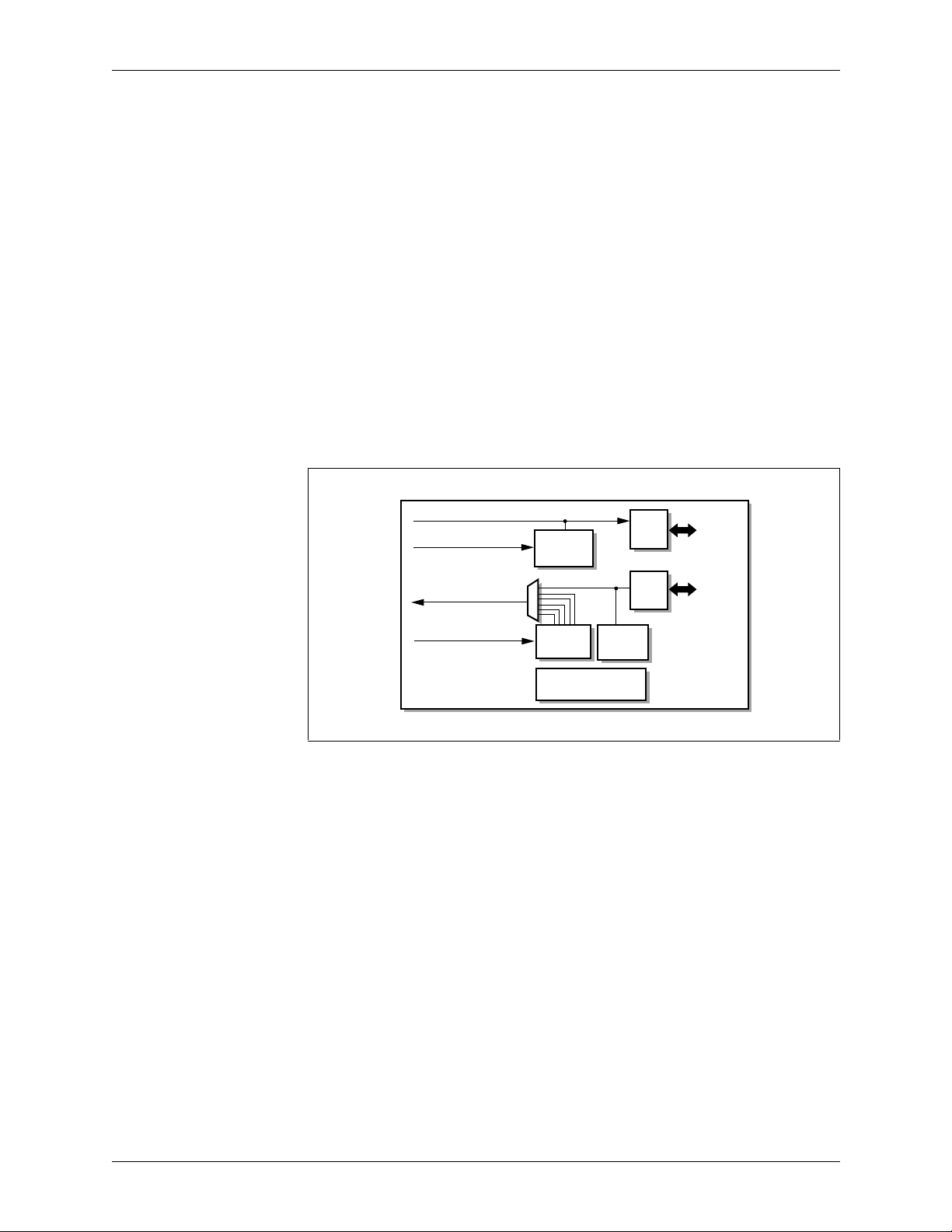
Figure 1-1. CX28395 Functional Block Diagram
Receive NRZ Data
Receive NRZ Clock
Transmit NRZ Data
Transmit NRZ Clock
T1/E1
Receive
Framer
Overhead
Insertion
Data Link Controllers
Transmit
DL1 + DL2
T1/E1
Framer
RX
Slip
Buffer
TX
Slip
Buffer
Receive
System
Bus
Transmit
System
Bus
8394-8-5_011
1-2 Conexant 100054E
Page 21

CX28394/28395/28398 1.0 Product Description
Quad/x16/Octal—T1/E1/J1 Framers
1.2 Pin Assignments
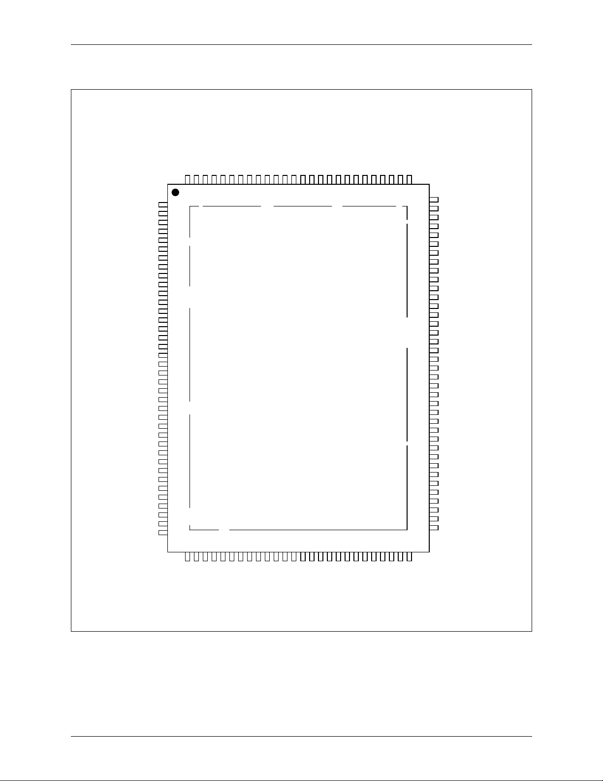
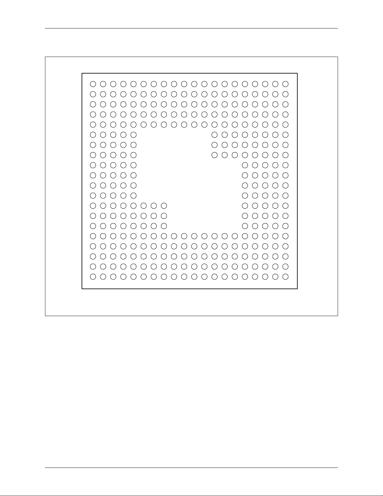
The CX28394 is packaged in a 128-pi n Quad Flat P ac k (TQFP). The CX 28395 is
packaged in a 318-pin Ball Grid Array (BGA) multi-chip module (MCM). The
CX28398 has two package alternatives: a 208-pin Quad Flat Pack (MQFP) and a
272-pin BGA. Pinout diagrams are provided in Figures 1-2 through 1-6 and
Tables 1-1 through 1-4 summarize pin assignments for system bus pins. Table 1-5
lists all other pin assignments.
the hardware signals.
remain unconnected if the active high input state is desired:
A[7:0] Address lines unused in INTEL bus mode.
MOTO* Pullup selects INTEL bus mode if unconnected.
SYNCMD Pullup selects synchronous processor interface.
TDI (CX28394/28398) JTAG unused if not connected.
TDI1, TDI2 (CX28395) JTAG unused if not connected.
TMS JTAG unused if not connected.
TCK Disables JTAG if not connected.
TRST* Disables JTAG reset if not connected.
RST* Disables hardware reset if not connected.
SERDI May be left unconnected if not used.
1.2 Pin Assignments
Figures 1-7 through 1-12 illustrate the devices’ logic, and Table 1-6 defines
The following input pins cont ain an i nt ernal pul lu p r esi sto r ( >50 k
Ω) and may
100054E Conexant 1-3
Page 22
1.0 Product Description CX28394/28395/28398
1.2 Pin Assignments Quad/x16/Octal—T1/E1/J1 Framers
Figure 1-2. CX28394 128-pin TQFP Pinout Di agram
TNEGO[4] / MSYNCO[4]
TCKI[4]
RCKI[4]
RPOSI[4]
RNEGI[4]
EIACKI
VSS
T1ACKI
VSS
SYSCKI
VSS
VDD
RPCMO[4] / RSIGO[4]
RFSYNC[4] / RMSYNC[4]
RSBCKI[4] / RFSYNC
SIGFRZ[4]
RSIGO[4] / RDLO[4]
RINDO[4] / RDLCKO[4]
TPCMI[4] / TSIGI[4]
TFSYNC[4] / TMSYNC[4]
TSBCKI[4] / TFSYNC
TSIGI[4] / TDLI[4]
TINDO[4] / TDLCKO[4]
VDD
RPCMO[3]/RSIGO[3]
RFSYNC[3] / RMSYNC[3]
RSBCKI[3] / RINDO
SIGFRZ[3]
RSIGO[3] / RDLO[3]
RINDO[3] / RDLCKO[3]
TPCMI[3] / TSIGI[3]
TFSYNC[3] / TMSYNC[3]
TSBCKI[3] / TINDO
TSIGI[3] / TDLI[3]
TINDO[3] / TDLCKO[3]
VGG
VSS
TRST*
RNEGI[3]
TCK0[4]
TPOSO[4] / TNRZO[4]
128
127
125
1
2
3
4
5
6
7
8
9
10
11
12
13
14
15
16
17
18
19
20
21
22
23
24
25
26
27
28
29
30
31
32
33
34
35
36
37
38
126
XMTR3 / RCVR3 XMTR1 / RCVR1
XMTR4 / RCVR4
CLKs
TSB4 / RSB4TSB3 / RSB3
JTAG
39
40434241444546474849505152535455565758596061626364
TPOSO[3] / TNRZO[3]
TNEGO[3] / MSYNCO[3]
VDD
124
123
122
121
120
119
118
XMTR2 / RCVR2
CX28394
117
RNEGI[2]
TCK0[3]
TCKI[3]
RCKI[3]
RPOSI[3]
TPOSO[2] / TNRZO[2]
TNEGO[2] / MSYNCO[2]
116
115
114
113
112
111
110
VDD
RNEGI[1]
TCK0[2]
TCKI[2]
RCKI[2]
RPOSI[2]
TPOSO[1] / TNRZO[1]
TNEGO[1] / MSYNCO[1]
TCKI[1]
RCKI[1]
RPOSI[1]
109
108
107
106
105
SERIO
MPU
SERCS1*
TCK0[1]
104
103
102
101
100
99
98
97
96
95
94
93
92
TSB1 / RSB1
91
90
89
88
87
86
85
84
83
82
81
80
79
TSB2 / RSB2
78
77
76
75
74
73
72
71
70
69
68
67
66
65
SERDI
SERDO
SERCKO
TINDO[1] / TDLCKO[1]
TSIGI[1] / TDLI[1]
TSBCKI[1] / TSBCKI
TFSYNC[1] / TMSYNC[1]
TPCMI[1] / TSIGI[1]
RINDO[1] / RDLCKO[1]
RSIGO[1] / RDLO[1]
SIGFRZ[1]
RSBCKI[1] / RSBCKI
RFSYNC[1] / RMSYNC[1]
RPCMO[1] / RSIGO[1]
VSS
VDD
VSS
TINDO[2] / TDLCKO[2]
TSIGI[2] / TDLI[2]
TSBCKI[2] / TPCMI
TFSYNC[2] / TMSYNC[2]
TPCMI[2] / TSIGI[2]
RINDO[2] / RDLCKO[2]
RSIGO[2] / RDLO[2]
SIGFRZ[2]
RSBCKI[2] / RPCMO
RFSYNC[2] / RMSYNC[2]
RPCMO[2] / RSIGO[2]
AD[0]
AD[1]
AD[2]
AD[3]
AD[4]
AD[5]
AD[6]
AD[7]
VSS
A[0]
TMS
TDI
TDO
TCK
VDD
ONESEC
INTR*
DTACK*
DS* / RD*
R/W* / WR*
CS*
AS* / ALE
MCLK
SYNCMD
RST*
MOTO*
A[9]
A[10]
A[8]
A[7]
A[6]
A[5]
A[4]
A[3]
A[2]
A[1]
8394-8-5_016
1-4 Conexant 100054E
Page 23
CX28394/28395/28398 1.0 Product Description
Quad/x16/Octal—T1/E1/J1 Framers
Figure 1-3. CX28395 318-pin BGA Pinout Diagram
1 2 3 4 5 6 7 8 9 10111213141516 171819 20
A
B
C
D
E
F
G
H
J
K
L
M
N
P
R
T
U
V
W
Y
Top View
1.2 Pin Assignments
A
B
C
D
E
F
G
H
J
K
L
M
N
P
R
T
U
V
W
Y
1 2 3 4 5 6 7 8 9 10111213141516 171819 20
8394-8-5_013
100054E Conexant 1-5
Page 24
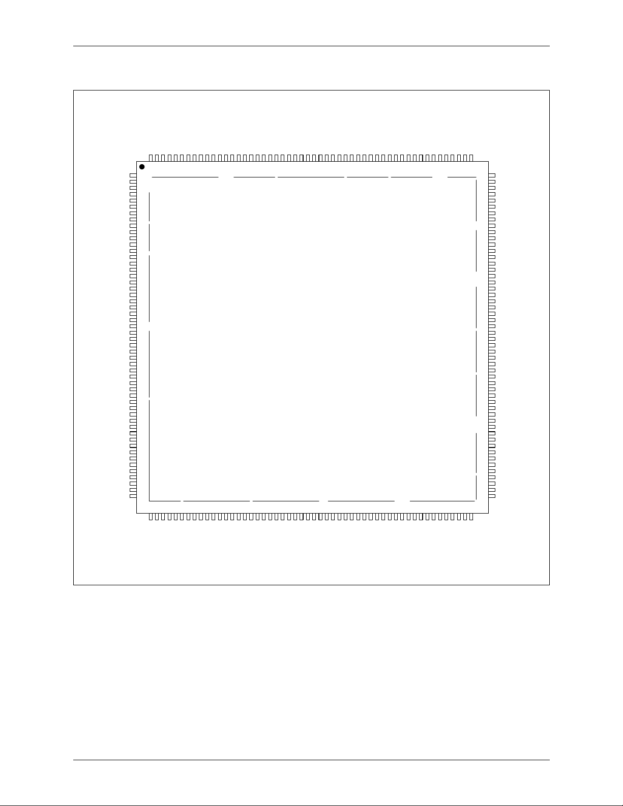
1.0 Product Description CX28394/28395/28398
1.2 Pin Assignments Quad/x16/Octal—T1/E1/J1 Framers
Figure 1-4. CX28398 208-pin PQFP Pinout Diagram
VGG
VSS
TRST*
TMS
TDO
FSYNC[8] / TMSYNC[8]
TSBCKI[8] / TFSYNC[B]
TINDO[8] / TDLCKO[8]
RPCMO[7] / RSIGO[7]
FSYNC[7] / RMSYNC[7]
RSBCKI[7] / RINDO[B]
RINDO[7] / RDLCKO[7]
FSYNC[7] / TMSYNC[7]
TSBCKI[7] / TINDO[B]
TINDO[7] / TDLCKO[7]
VDD
TSIGI[8] / TDLI[8]
ONESEC
INTR*
DTACK*
R/W* / WR*
DS* / RD*
AS* / ALE
MCLK
SYNCMD
MOTO*
RST*
VSS
SIGFRZ[7]
RSIGO[7] / RDLO[7]
TPCMI[7] / TSIGI[7]
TSIGI[7] / TDLI[7]
A[11]
A[10]
VDD
VSS
AD[7]
AD[6]
AD[5]
TCK
3
VSS
TINDO[3] / TDLCKO[3]
TSIGI[3] / TDLI[3]
TSBCKI[3] / TINDO[A]
TPCMI[3] / TSIGI[3]
RINDO[3] / RDLCKO[3]
RSIGO[3] / RDLO[3]
TFSYNC[3] / TMSYNC[3]
208
206
205
204
203
MPU
MPU
202
55
56
57
58
59
207
1
2
3
4
5
TDI
6
JTAG
7
8
9
10
TSB8 / RSB8
11
12
13
14
15
16
17
CS*
18
19
20
21
22
23
24
25
26
27
28
29
30
31
TSB7 / RSB7
32
33
34
35
36
37
A[9]
38
39
A[8]
A[7]
40
A[6]
41
42
A[5]
43
A[4]
44
A[3]
45
A[2]
A[1]
46
47
A[0]
48
49
50
51
52
53
54
VDD
SIGFRZ[3]
RSBCKI[3] / RINDO[A]
201
200
60
61
TPCMI[8] / TSIGI[8]
RPCMO[3]/RSIGO[3]
RFSYNC[3] / RMSYNC[
199
198
197
196
195
TSB6 / RSB6 TSB5 / RSB5TSB2 / RSB2 TSB1 / RSB1
62
63
64
65
66
8
TINDO[4] / TDLCKO[4]
TSIGI[4] / TDLI[4]
TSBCKI[4] / TFSYNC[A]
TPCMI[4] / TSIGI[4]
TFSYNC[4] / TMSYNC[4]
RINDO[8] / RDLCKO[8]
194
RPCMO[8] / RSIGO[8]
RSIGO[8] / RDLO[8]
SIGFRZ[8]
RSBCKI[8] / RFSYNC[B]
RFSYNC[8] / RMSYNC[
193
192
191
190
189
188
187
186
185
184
TSB8 / RSB8 TSB4 / RSB4TSB3 / RSB3 CLKsXMTR8 / RCVR8 XMTR7 / RCVR7
RINDO[4] / RDLCKO[4]
RSIGO[4] / RDLO[4]
SIGFRZ[4]
RSBCKI[4] / RFSYNC[A]
181
180
183
182
4
RNEGI[8]
RPOSI[8]
RCKI[8]
RPCMO[4] / RSIGO[4]
RFSYNC[4] / RMSYNC[
179
TCKI[8]
178
177
176
175
174
TNEGO[8] / MSYNCO[8]
TPOSO[8] / TNRZO[8]
TCK0[8]
RNEGI[7]
RPOSI[7]
RCKI[7]
TCKI[7]
173
172
171
170
169
168
167
CX28398
67
68
69
70
71
72
73
74
75
76
77
78
79
80
81
82
83
84
85
86
87
88
89
90
91
92
93
94
TNEGO[7] / MSYNCO[7]
TPOSO[7] / TNRZO[7]
TCK0[7]
VDD
VSS
SYSCKI
166
165
164
163
162
161
XMTR4 / RCVR4
XMTR3 / RCVR3
XMTR6 / RCVR6
XMTR2 / RCVR2
XMTR5 / RCVR5
XMTR1 / RCVR1
95
96
97
98
99
100
VSS
160
101
T1ACKI
159
SERIO
102
VSS
158
103
EIACKI
157
156
155
154
153
152
151
150
149
148
147
146
145
144
143
142
141
140
139
138
137
136
135
134
133
132
131
130
129
128
127
126
125
124
123
122
121
120
119
118
117
116
115
114
113
112
111
110
109
108
107
106
105
104
RNEGI[4]
RPOSI[4]
RCKI[4]
TCKI[4]
TNEGO[4] / MSYNCO
TPOSO[4] / TNRZO[4]
TCK0[4]
VDD
RNEGI[3]
RPOSI[3]
RCKI[3]
TCKI[3]
TNEGO[3] / MSYNCO
TPOSO[3] / TNRZO[3
TCK0[3]
VDD
VSS
RNEGI[6]
RPOSI[6]
RCKI[6]
TCKI[6]
TNEGO[6] / MSYNCO
TPOSO[6] / TNRZO[6
TCK0[6]
RNEGI[2]
RPOSI[2]
RCKI[2]
TCKI[2]
TNEGO[2] / MSYNCO
TPOSO[2] / TNRZO[2
TCK0[2]
RNEGI[5]
RPOSI[5]
RCKI[5]
TCKI[5]
TNEGO[5] / MSYNCO
TPOSO[5] / TNRZO[5
TCK0[5]
VDD
VSS
RNEGI[1]
RPOSI[1]
RCKI[1]
TCKI[1]
TNEGO[1] / MSYNCO
TPOSO[1] / TNRZO[1
TCK0[1]
SERCS2*
SERCS1*
SERDI
SERDO
SERCKO
]
]
]
]
]
TSIGI[5] / TDLI[5]
TSBCKI[5] / TSBCKI[B]
TFSYNC[5] / TMSYNC[5]
VDD
VSS
TINDO[5] / TDLCKO[5]
SIGFRZ[1]
RSIGO[1] / RDLO[1]
RPCMO[1] / RSIGO[1]
RINDO[1] / RDLCKO[1]
RSBCKI[1] / RSBCKI[A]
FSYNC[1] / RMSYNC[1]
R
TPCMI[1] / TSIGI[1]
TFSYNC[1] / TMSYNC[1]
TSIGI[1] / TDLI[1]
TSBCKI[1] / TSBCKI[A]
TINDO[1] / TDLCKO[1]
8394-8-5_023
AD[4]
AD[3]
AD[2]
AD[1]
AD[0]
RPCMO[6] / RSIGO[6]
FSYNC[6] / RMSYNC[6]
R
SIGFRZ[6]
TPCMI[6] / TSIGI[6]
RSIGO[6] / RDLO[6]
RINDO[6] / RDLCKO[6]
RSBCKI[6] / RPCMO[B]
FSYNC[6] / TMSYNC[6]
T
TSIGI[6] / TDLI[6]
TSBCKI[6] / TPCMI[B]
TINDO[6] / TDLCKO[6]
SIGFRZ[2]
RSIGO[2] / RDLO[2]
RPCMO[2] / RSIGO[2]
RINDO[2] / RDLCKO[2]
RSBCKI[2] / RPCMO[A]
FSYNC[2] / RMSYNC[2]
R
TPCMI[2] / TSIGI[2]
TFSYNC[2] / TMSYNC[2]
TSIGI[2] / TDLI[2]
TSBCKI[2] / TPCMI[A]
VSS
RPCMO[5] / RSIGO[5]
TINDO[2] / TDLCKO[2]
FSYNC[5] / RMSYNC[5]
R
SIGFRZ[5]
TPCMI[5] / TSIGI[5]
RSIGO[5] / RDLO[5]
RINDO[5] / RDLCKO[5]
RSBCKI[5] / RSBCKI[B]
1-6 Conexant 100054E
Page 25

CX28394/28395/28398 1.0 Product Description
Quad/x16/Octal—T1/E1/J1 Framers
Figure 1-5. CX28398 208-pin CABGA Pinout Diagram
23456789101112131415161 17
A
B
C
D
E
F
G
H
J
Top View
1.2 Pin Assignments
A
B
C
D
E
F
G
H
J
K
L
M
N
P
R
T
U
23456789101112131415161 17
K
L
M
N
P
R
T
U
100054_001
100054E Conexant 1-7
Page 26
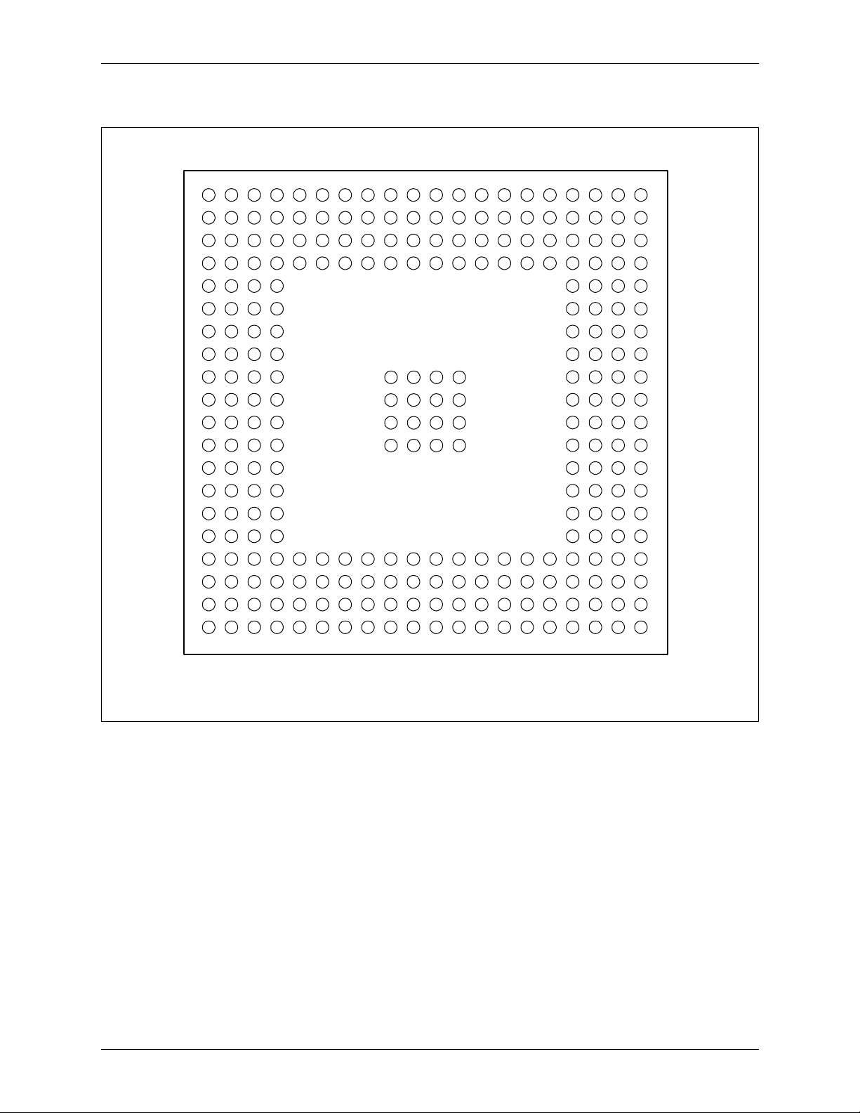
1.0 Product Description CX28394/28395/28398
1.2 Pin Assignments Quad/x16/Octal—T1/E1/J1 Framers
Figure 1-6. CX28398 272-pin BGA Pinout Diagram
1 2 3 4 5 6 7 8 9 10111213141516 171819 20
A
B
C
D
E
F
G
H
J
K
L
M
N
P
R
T
U
V
W
Y
Top View
A
B
C
D
E
F
G
H
J
K
L
M
N
P
R
T
U
V
W
Y
1 2 3 4 5 6 7 8 9 10111213141516 171819 20
8394-8-5_005
1-8 Conexant 100054E
Page 27

CX28394/28395/28398 1.0 Product Description
Quad/x16/Octal—T1/E1/J1 Framers
Table 1-1. Pin Assignments (SBI1, SBI2, SBI3, SBI4) (1 of 2)
Pin Number System Bus Interface Pin Functions
Non-Multiplexed Mode
CX28394
89 94 R12 V15 J3 RPCMO[1] RSIGO[1]
90 95 P11 W16 J4 RFSYNC[1]/RMSYNC[1] RMSYNC[1]
91 96 U14 Y17 J2 RSBCKI[1] RSBCKI[A]
92 97 T14 V16 — SIGFRZ[1] SIGFRZ[1]
93 98 R13 W17 — RSIGO[1] / RDLO[1] RDLO [ 1]
————J1RSIGO[1] TSTO[1]
94 99 P12 Y18 — RINDO[1] / RDLCKO[1] RDLCKO[1]
95 100 U15 V17 K4 TPCMI[1] TSIGI[1]
96 101 U16 W18 K1 TFSYNC[1]/TMSYNC[1] TMSYNC[1]
128-pin TQFP
CX28398
208-pin PQFP
CX28398
208-pin CABGA
CX28398
CX28395
272-pin BGA
318-pin BGA
SBIMODE[0] = 0 [FCR; addr 080]
SBIMODE[0] = 1 [FCR; addr 080]
1.2 Pin Assignments
Multiplexed Mode
97 102 R14 Y19 K3 TSBCKI[1] TSBCKI[A]
98 103 P13 V18 — TSIGI[1] / TDLI [1] TDLI[1]
— — — — K2 TSIGI[1] TSTI[1]
99 104 T15 W19 — TINDO[1] / TDLCKO[1] TDLCKO[1]
————K5TINDO[1] —
75 69 R6 W8 E4 RPCMO[2] RSIGO[2]
76 70 T6 Y8 E3 RFSYNC[2]/RMSYNC[2] RMSYNC[2]
77 71 U7 V9 E2 RSBCKI[2] RPCMO[A]
78 72 P7 W9 — SIGFRZ[2] SIGFRZ[2]
79 73 R7 Y9 — RSIGO[2] / RDLO[2] R DLO[2]
————F4RSIGO[2] TSTO[2]
80 74 T7 W10 — RINDO[2] / RDLCKO[2] RDLCKO[2 ]
81 75 U8 V10 F3 TPCMI[2] TSIGI[2]
82 76 P8 Y10 F2 TFSYNC[2]/TMSYNC[2] TMSYNC[2]
83 77 R8 Y11 E1 TSBCKI[2] TPCMI[A]
84 78 T8 W 11 — TSIGI[2] / TDLI[2] TDLI[2]
— — — — F1 TSIGI[2] TSTI[2]
85 79 U9 V11 — TINDO[2] / TDLCKO[2] TDLCKO[2]
— — — — H5 TINDO[2] —
25 198 C6 C6 U9 RPCMO[3] RSIGO[3]
26 199 D6 B5 Y9 RFSYNC[3]/RMSYNC[3] RMSYNC[3]
100054E Conexant 1-9
Page 28

1.0 Product Description CX28394/28395/28398
1.2 Pin Assignments Quad/x16/Octal—T1/E1/J1 Framers
Table 1-1. Pin Assignments (SBI1, SBI2, SBI3, SBI4) (2 of 2)
Pin Number System Bus Interface Pin Functions
Non-Multiplexed Mode
SBIMODE[0] = 0 [FCR; addr 080]
CX28394
27 200 C5 A4 U10 RSBCKI[3] RINDO[A]
28 201 D5 C5 — SIGFRZ[3] SIGFRZ[3]
29 202 B5 B4 — RSIGO[3] / RDLO[3] RDLO [ 3]
————Y10RSIGO[3] TSTO[3]
30 203 A4 A3 — RINDO[3] / RDLCKO[3] RDLCKO[3]
31204A3C4V9TPCMI[3] TSIGI[3]
32 205 B3 B3 W10 TFSYNC[3]/TMSYNC[3] TMSYNC[3]
33 206 C4 B2 V10 TSBCKI[3] TINDO[A]
34 207 A2 A2 — TSIGI[3] / TDLI[3] TDLI[3]
— — — — W9 TSIGI[3] TSTI[3]
35 208 B4 C3 — TINDO[3] / TDLCK O[ 3] TDLCKO[3]
————T10TINDO[3] —
13 178 A11 B11 U5 RPCMO[4] RSIGO[4]
14 179 B10 C11 W5 RFSYNC[4]/RMSYNC[4] RMSYNC[4]
CX28398
128-pin TQFP
208-pin PQFP
CX28398
CX28398
208-pin CABG A
CX28395
272-pin BGA
318-pin BGA
Multiplexed Mode
SBIMODE[0] = 1 [FCR; addr 080]
15 180 C10 A11 V6 RSBCKI[4] RFSYNC[A]
16 181 D10 A10 — SIGFRZ[4] SIGFRZ[4]
17 182 A10 B10 — RSIGO[4] / RDLO[4] RDLO[4]
————Y5RSIGO[4] TSTO[4]
18 183 A9 C10 — RINDO[4] / RDLCKO[4] RDLCKO[4]
19 184 B9 A9 W6 TPCMI[4] TSIGI[4]
20 185 C9 B9 V5 TFSYNC[4]/TMSYNC[4] TMSYNC[4]
21 186 D9 C9 U6 TSBCKI[4] TFSYNC[A]
22 187 A8 A8 — TSIGI[4] / TDLI[4] TDLI[4]
— — — — Y6 TSIGI[4] TSTI[4]
23 188 C8 B8 — TINDO[4] / TDLCK O[ 4] TDLCKO[4]
————T8TINDO[4] —
1-10 Conexant 100054E
Page 29

CX28394/28395/28398 1.0 Product Description
Quad/x16/Octal—T1/E1/J1 Framers
Table 1-2. Pin Assignments (SBI5, SBI6, SBI7, SBI8) (1 of 2)
Pin Number System Bus Interface Pin Functions Pin Functions
Non-Multiplexed Mode
CX28394
— 81 U10 Y12 G4 RPCMO[5] RSIGO[5]
— 82 R9 W12 G2 RFSYNC[5] / RMSYNC[5] RMSYNC[5]
— 83 P9 V12 G3 RSBCKI[5] RSBCKI[B]
— 84 T10 Y13 — SIGFRZ[5] SIGFRZ[5]
— 85 R10 W13 — RSIGO[5] / RDLO[5] RDLO [5]
————G1RSIGO[5] TSTO[5]
— 86 U11 V13 — RINDO[5] / RDLCKO[5] RDLCKO[5]
— 87 T11 Y14 H3 TPCMI[5] TSIGI[5]
— 88 R11 W14 H4 TFSYNC[5] / TMSYNC[5] TMSYNC[5]
128-pin TQFP
CX28398
208-pin PQFP
CX28398
208-pin CABGA
CX28398
CX28395
272-pin BGA
318-pin BGA
SBIMODE[0] = 0 [FCR; addr 080]
SBIMODE[0] = 1 [FCR; addr 080]
1.2 Pin Assignments
Multiplexed Mode
— 89 T12 Y15 H1 TSBCKI[5] TSBCKI[B]
— 90 U12 V14 — TSIGI[5] / TDLI[5] TDLI[5]
— — — — H2 TSIGI[5] TSTI[5]
— 91 P10 W15 — TINDO[5] / TDLCKO[5] TDLCK O[ 5]
————J5TINDO[5] —
—58P4Y4C2RPCMO[6] RSIGO[6]
— 59 U3 V5 C4 RFSYNC[6] / RMSYNC[6] RMSYNC[6]
— 60 U4 W5 C1 RSBCKI[6] RPCMO[B]
— 61 R4 Y5 — SIGFRZ[6] SIGFRZ[6]
— 62 T4 V6 — RSIGO[6] / RDLO[6] RDLO[ 6]
————D4RSIGO[6] TSTO[6]
— 63 U5 W6 — RINDO[6] / RDLCKO[6] RDLCKO[6 ]
— 64 P5 Y6 D2 TPCMI[6] TSIGI[6]
— 65 R5 V7 D3 TFSYNC[6] / TMSYNC[6] TMSYNC[6]
— 66 T5 W7 D1 TSBCKI[6] TPCMI[B]
— 67 U6 Y 7 — TS IGI[6] / TDLI[6] TDLI[6]
— — — — C3 TSIGI[6] TSTI[6]
— 68 P6 V8 — TI NDO[6] / TDLCKO[6] TDLCKO[6]
— — — — G5 TINDO[6] —
— 25 J4 L1 U12 RPCMO[7] RSIGO[7]
— 26 H2 L2 Y11 RFSYNC[7] / RMSYNC[7] RMSYNC[7]
100054E Conexant 1-11
Page 30

1.0 Product Description CX28394/28395/28398
1.2 Pin Assignments Quad/x16/Octal—T1/E1/J1 Framers
Table 1-2. Pin Assignments (SBI5, SBI6, SBI7, SBI8) (2 of 2)
Pin Number System Bus Interface Pin Functions Pin Functions
Non-Multiplexed Mode
SBIMODE[0] = 0 [FCR; addr 080]
CX28394
— 27 H1 L3 Y12 RSBCKI[7] RINDO[B]
—28J1M1—SIGFRZ[7] SIGFRZ[7]
— 29 J3 M2 — RSIGO[7] / RDLO[7] RDLO[7]
————W11RSIGO[7] TSTO[7]
— 30 J2 M3 — RINDO[7] / RDLCKO[7] RDLCKO[7]
— 31 K4 N1 W12 TPCMI[7] TSIGI[7]
— 32 K1 N2 V11 TFSYNC[7] / TMSYNC[7] TMSYNC[7]
— 33 K2 N3 V12 TSBCKI[7] TINDO[B]
— 34 L 1 P1 — TSIGI[7] / TDLI[7] TDLI[7]
————U11TSIGI[7] TSTI[7]
— 35 K3 P2 — TI NDO[7] / TDLCKO[7] TDLCKO[7]
————T11TINDO[7] —
— 189 D8 C8 W7 RPCMO[8] RSIGO[8]
— 190 B8 A7 V7 RFSYNC[8] / RMSYNC[8] RMSYNC[8]
CX28398
128-pin TQFP
208-pin PQFP
CX28398
CX28398
208-pin CABG A
CX28395
272-pin BGA
318-pin BGA
Multiplexed Mode
SBIMODE[0] = 1 [FCR; addr 080]
— 191 C7 B7 Y7 RSBCKI[8] RFSYNC[B]
— 192 A7 A6 — SIGFRZ[8] SIGFRZ[8]
— 193 D7 C7 — RSIGO[8] / RDLO[8] RDLO[8]
————V8RSIGO[8] TSTO[8]
— 194 B7 B6 — RINDO[8] / RDLCKO[8] RDLCKO[8]
— 195 A6 A5 Y8 TPCMI[8] TSIGI[8]
— 9 E4 E1 W8 TFSYNC[8] / TMSYNC[8] TMSYNC[8]
— 10 E3 F3 U8 TSBCKI[8] TFSYNC[B]
— 11 D2 F2 — TSIGI[8] / TDLI[8] TDLI[8]
— — — — U7 TSIGI[8] TSTI[8]
— 12 D1 F1 — TINDO[ 8] / TDLCKO[8] TDLCKO[8]
————T9TINDO[8] —
1-12 Conexant 100054E
Page 31

CX28394/28395/28398 1.0 Product Description
Quad/x16/Octal—T1/E1/J1 Framers
Table 1-3. Pin Assignments (SBI9, SBI10, SBI11, SBI12) (1 of 2)
Pin Number System Bus Interface Pin Functions
Non-Multiplexed Mode
CX28394
— — — — F20 RPCMO[9] RSIGO[9]
— — — — F18 RFSYNC[9]/RMSYNC[9] RMSYNC[9]
— — — — F19 RSBCKI[9] RSBCKI[C]
————F17RSIGO[9] TSTO[9]
————E20TPCMI[9] TSIGI[9]
— — — — E18 TFSYNC[9]/TMSYNC[9] TMSYNC[9]
— — — — E19 TSBCKI[9] TSBCKI[C]
————E17TSIGI[9] TSTI[9]
————F16TINDO[9] —
128-pin TQFP
CX28398
208-pin PQFP
CX28398
208-pin CABGA
CX28398
CX28395
272-pin BGA
318-pin BGA
SBIMODE[0] = [FCR; ad dr 001]
SBIMODE[0] = 1 [FCR; addr 001]
1.2 Pin Assignments
Multiplexed Mode
— — — — K17 RPCMO[10] RSIGO[10]
— — — — K19 RFSYNC[10]/RMSYNC[10] RMSYNC[10]
— — — — K18 RSBCKI[10] RPCMO[C]
————K20RSIGO[10] TSTO[10]
————J17TPCMI[10] TSIGI[10]
— — — — J20 TFSYNC[10]/TMSYNC[10] TMSYNC[10]
— — — — J18 TSBCKI[10] TPCMI[C]
— — — — J19 TSIGI[10] TSTI[10]
————H16TINDO[10] —
— — — — A4 RPCMO[11] RSIGO[11]
— — — — A3 RFSYNC[11]/RMSYNC[11] RMSYNC[11]
— — — — B4 RSBCKI[11] RINDO[C]
————B3RSIGO[11] TSTO[11]
————A2TPCMI[11] TSIGI[11]
— — — — A1 TFSYNC[11]/TMSYNC[11] TMSYNC[11]
— — — — B2 TSBCKI[11] TINDO[C]
— — — — B1 TSIGI[11] TSTI[11]
————E5TINDO[11] —
— — — — A10 RPCMO[12] RSIGO[12]
— — — — D10 RFSYNC[12]/RMSYNC[12] RMSYNC[12]
— — — — B10 RSBCKI[12] RFSYNC[C]
100054E Conexant 1-13
Page 32

1.0 Product Description CX28394/28395/28398
1.2 Pin Assignments Quad/x16/Octal—T1/E1/J1 Framers
Table 1-3. Pin Assignments (SBI9, SBI10, SBI11, SBI12) (2 of 2)
Pin Number System Bus Interface Pin Functions
Non-Multiplexed Mode
CX28394
— — — — D9 RSIGO[12] TSTO[12]
————A9TPCMI[12] TSIGI[12]
— — — — C9 TFSYNC[12]/TMSYNC[12] TMSYNC[12]
— — — — B9 TSBCKI[12] TFSYNC[C]
— — — — C10 TSIGI[12] TSTI[12]
————E7TINDO[12] —
CX28398
128-pin TQFP
208-pin PQFP
CX28398
CX28398
208-pin CABG A
CX28395
272-pin BGA
318-pin BGA
SBIMODE[0] = [FCR; ad dr 001]
SBIMODE[0] = 1 [FCR; addr 001]
Table 1-4. Pin Assignments (SBI13, SBI14, SBI15, SBI16) (1 of 2)
Pin Number System Bus Interface Pin Functions
Non-Multiplexed Mode
CX28394
CX28398
128-pin TQFP
CX28398
208-pin PQFP
208-pin CABGA
CX28398
CX28395
272-pin BGA
318-pin BGA
SBIMODE[0] = [FCR; ad dr 001]
SBIMODE[0] = 1 [FCR; addr 001]
Multiplexed Mode
Multiplexed Mode
— — — — H18 RPCMO[13] RSIGO[13]
— — — — H19 RFSYNC[13]/RMSYNC[13] RMSYNC[13]
— — — — H17 RSBCKI[13] RSBCKI[D]
————H20RSIGO[13] TSTO[13]
————G17TPCMI[13] TSIGI[13]
— — — — G20 TFSYNC[13]/TMSYNC[13] TMSYNC[13]
— — — — G18 TSBCKI[13] TSBCKI[D]
— — — — G19 TSIGI[13] TSTI[13]
————G16TINDO[13] —
— — — — M18 RPCMO[14] RSIGO[14]
— — — — M17 RFSYNC[14]/RMSYNC[14] RMSYNC[14]
— — — — M19 RSBCKI[14] RPCMO[D]
— — — — L19 RSIGO[14] TSTO[14]
— — — — L20 TPCMI[14] TSIGI[14]
— — — — L17 TFSYNC[14]/TMSYNC[14] TMSYNC[14]
— — — — M20 TSBCKI[14] TPCMI[D]
1-14 Conexant 100054E
Page 33

CX28394/28395/28398 1.0 Product Description
Quad/x16/Octal—T1/E1/J1 Framers
Table 1-4. Pin Assignments (SBI13, SBI14, SBI15, SBI16) (2 of 2)
Pin Number System Bus Interface Pin Functions
Non-Multiplexed Mode
CX28394
— — — — L18 TSIGI[14] TSTI[14]
————K16TINDO[14] —
— — — — B7 RPCMO[15] RSIGO[15]
— — — — B8 RFSYNC[15]/RMSYNC[15] RMSYNC[15]
— — — — D7 RSBCKI[15] RINDO[D]
————C8RSIGO[15] TSTO[15]
————A7TPCMI[15] TSIGI[15]
— — — — A8 TFSYNC[15]/TMSYNC[15] TMSYNC[15]
— — — — C7 TSBCKI[15] TINDO[D]
CX28398
128-pin TQFP
208-pin PQFP
CX28398
CX28398
208-pin CABG A
CX28395
272-pin BGA
318-pin BGA
SBIMODE[0] = [FCR; ad dr 001]
SBIMODE[0] = 1 [FCR; addr 001]
1.2 Pin Assignments
Multiplexed Mode
— — — — D8 TSIGI[15] TSTI[15]
————M16TINDO[15] —
— — — — A6 RPCMO[16] RSIGO[16]
— — — — A5 RFSYNC[16]/RMSYNC[16] RMSYNC[16]
— — — — B6 RSBCKI[16] RFSYNC[D]
— — — — D6 RSIGO[16] TSTO[16]
————C6TPCMI[16] TSIGI[16]
— — — — B5 TFSYNC[16]/TMSYNC[16] TMSYNC[16]
— — — — C5 TSBCKI[16] TFSYNC[D]
— — — — D5 TSIGI[16] TSTI[16]
————J16TINDO[16] —
100054E Conexant 1-15
Page 34

1.0 Product Description CX28394/28395/28398
1.2 Pin Assignments Quad/x16/Octal—T1/E1/J1 Framers
Table 1-5. Pin Assignments (1 of 9)
Pin Number
Pin Functio ns
CX28394
7 117 B2 A1 N6 VSS (GND)
9 140 G1 D4 N7 VSS (GND)
11 158 P3 D8 N8 VSS (GND)
37 160 T9 D13 P6 VSS (GND)
66 162 T13 D17 P7 VSS (GND)
86 196 N17 H4 P8 VSS (GND)
— 2 F17 H17 R6 VSS (GND)
— 24 B16 J9 R7 VSS (GND)
— 49 A16 J10 R8 VSS (GND)
— 80 D14 J11 F13 VSS (GND)
— 93 B6 J12 F14 VSS (GND)
— — — K9 F15 VSS (GND)
— — — K10 G13 VSS (GND)
— — — K11 G14 VSS (GND)
— — — K12 G15 VSS (GND)
128-pin TQFP
CX28398
208-pin PQFP
CX28398
208-pin CABGA
CX28398
CX28395
272-pin BGA
318-pin BGA
———L9H13VSS (GND)
— — — L10 H14 VSS (GND)
— — — L11 H15 VSS (GND)
— — — L12 T13 VSS ( GND)
———M9T14VSS (GND)
— — — M10 — VSS (GND)
— — — M11 — VSS (GND)
— — — M12 — VSS (GND)
— — — N4 — VSS (GND)
— — — N17 — VSS (GND)
— — — U4 — VSS (GND)
— — — U8 — VSS (GND)
— — — U13 — VSS (GND)
— — — U17 — VSS (GND)
111 118 C1 D6 E6 VDD
1-16 Conexant 100054E
Page 35

CX28394/28395/28398 1.0 Product Description
Quad/x16/Octal—T1/E1/J1 Framers
Table 1-5. Pin Assignments (2 of 9)
119 141 P2 D11 F5 VDD
Pin Number
Pin Functio ns
CX28394
12 149 U13 D15 N20 VDD
24 163 M15 F4 R16 VDD
43 197 G15 F17 T15 VDD
87 8 F14 K4 Y20 VDD
—48C14L17—VDD
—92A5R4—VDD
———R17—VDD
— — — U6 — VDD
CX28398
128-pin TQFP
208-pin PQFP
CX28398
CX28398
208-pin CABG A
CX28395
272-pin BGA
318-pin BGA
1.2 Pin Assignments
———U10—VDD
———U15—VDD
36 1 A1 B1 Y14 VGG
38 3 C3 D2 Y16 TRST*
39 4 B1 D3 W20 TMS
40 5 D4 C1 — TDI
————Y15TDI1
————T20TDI2
41 6 D3 D1 — TD0
————Y19TDO1
————P19TDO2
42 7 C2 E3 W17 TCK
6 157 A17 A19 P20 E1ACKI
8 159 B15 B17 N19 T1ACKI
10 161 C15 A18 U13 SYSCKI
44 13 F4 G3 — ONESEC
————V13ONESEC1
————Y13ONESEC2
45 14 F3 G2 — INTR*
————Y18INTR1*
————N17INTR2*
100054E Conexant 1-17
Page 36

1.0 Product Description CX28394/28395/28398
1.2 Pin Assignments Quad/x16/Octal—T1/E1/J1 Framers
Table 1-5. Pin Assignments (3 of 9)
Pin Number
Pin Functio ns
CX28394
46 15 E2 G1 — DTACK*
————W13DTACK1*
————T18DTACK2*
47 16 E1 H3 Y17 R/W*/WR*
48 17 G4 H2 W14 DS*/RD*
49 18 G3 H1 — CS*
————W19CSI*
————N18CS2*
50 19 F2 J3 V14 AS*/ALE
51 20 F1 J2 U14 MCLK
52 21 H4 J1 W15 SYNCMD
53 22 H3 K2 W18 MOTO*
54 23 G2 K3 W16 RST*
— 36 L3 R1 V15 A[11]
55 37 M2 P3 V18 A[10]
CX28398
128-pin TQFP
208-pin PQFP
CX28398
CX28398
208-pin CABG A
CX28395
272-pin BGA
318-pin BGA
56 38 M1 R2 U15 A[9]
57 39 L4 T1 V16 A[8]
58 40 N2 R3 V20 A[7]
59 41 L2 T2 V19 A[6]
60 42 N1 U1 U20 A[5]
61 43 M4 T3 V17 A[4]
62 44 M3 U2 U16 A[3]
63 45 N4 V1 U19 A[2]
64 46 P1 U3 U17 A[1]
65 47 N3 V2 T17 A[0]
67 50 R2 V3 R17 AD[7]
68 51 R1 W2 U18 AD[6]
69 52 T1 Y1 R18 AD[5]
70 53 U1 W3 R20 AD[4]
71 54 T2 Y2 P18 AD[3]
1-18 Conexant 100054E
Page 37

CX28394/28395/28398 1.0 Product Description
Quad/x16/Octal—T1/E1/J1 Framers
Table 1-5. Pin Assignments (4 of 9)
100 105 U17 W20 — SERCLKO
101 106 T16 V19 — SERDO
102 107 T17 U19 — SERDI
103 108 R16 U18 — SERCS1* (SERCS *)
104 110 R15 U20 L3 TCKO[1]
Pin Number
Pin Functio ns
CX28394
72 55 U2 W4 R19 AD2]
73 56 T3 V4 P17 AD[1]
74 57 R3 Y3 T19 AD[0]
— 109 R17 V20 — SERCS2*
CX28398
128-pin TQFP
208-pin PQFP
CX28398
CX28398
208-pin CABG A
CX28395
272-pin BGA
318-pin BGA
1.2 Pin Assignments
107 113 P16 T20 M3 TCKI[1]
105 111 N15 T18 L4 TPOSO[1]/TNRZO[1]
106 112 P17 T19 L5 TNEGO[1]/MSYNCO[1]
108 114 P15 R18 L1 RCKI[1]
109 115 P14 R19 L2 RPOSI[1]/RNRZI[1]
110 116 N16 R20 — RNEGI[1]
112 126 K15 L19 N1 TCKO[2]
115 129 K16 K20 P3 TCKI[2]
113 127 K17 L18 N2 TPOSO[2]/TNRZO[2]
114 128 L14 L20 N5 TNEGO[2]/MSYNCO[2]
116 130 J16 K19 P1 RCKI[2]
117 131 J17 K18 P2 RPOSI[2]/RNRZI[2]
118 132 J15 J20 — RNEGI[2]
120 142 H14 F19 T1 TCKO[3]
123 145 G14 E19 T4 TCKI[3]
121 143 F16 E20 T3 TPOSO[3]/TNRZO[3]
122 144 E17 F18 R5 TNEGO[3]/MSYNCO[3]
124 146 F15 D20 T2 RCKI[3]
125 147 E16 E18 U1 RPOSI[3]/RNRZI[3]
126 148 D17 D19 — RNEGI[3]
127 150 E15 C20 U2 TCKO[4]
100054E Conexant 1-19
Page 38

1.0 Product Description CX28394/28395/28398
1.2 Pin Assignments Quad/x16/Octal—T1/E1/J1 Framers
Table 1-5. Pin Assignments (5 of 9)
Pin Number
Pin Functio ns
CX28394
2 153 E14 B20 U3 TCKI[4]
128 151 D16 D18 U4 TPOSO[4]/TNRZO[4]
1 152 C17 C19 T5 TNEGO[4]/MSYNCO[4]
3 154 D15 C18 V1 RCKI[4]
4 155 C16 B19 V2 RPOSI[4]/RNRZI[4]
5 156 B17 A20 — RNEGI[4]
— 119 N14 P20 M4 TCKO[5]
— 122 L15 N20 M2 TCKI[5]
— 120 M16 N18 M1 TPOSO[5]/TNRZO[5]
— 121 M17 N19 M5 TNEGO[5]/MSYNCO[5]
— 123 M14 M18 N3 RCKI[5]
— 124 L16 M19 N4 RPOSI[5]/RNRZI[5]
— 125 L17 M20 — RNEGI[5]
— 133 H17 J19 P4 TCKO[6]
— 136 H15 H19 R2 TCKI[6]
CX28398
128-pin TQFP
208-pin PQFP
CX28398
CX28398
208-pin CABG A
CX28395
272-pin BGA
318-pin BGA
— 134 K14 J18 R1 TPOSO[6]/TNRZO[6]
— 135 H16 H20 P5 TNEGO[6]/MSYNCO[6]
— 137 G17 H18 R3 RCKI[6]
— 138 J14 G20 R4 RPOSI[6] /RNRZI[6]
— 139 G16 G19 — RNEGI[6]
— 164 B14 B16 V3 TCKO[7]
— 167 C13 B15 Y1 TCKI[7]
— 165 A15 A16 W1 TPOSO[7]/TNRZO[7]
— 166 D13 C15 T6 TNEGO[7]/MSYNCO[7]
— 168 A14 A15 W2 RCKI[7]
— 169 B13 C14 Y2 RPOSI[7] /RNRZI[7]
— 170 D12 B14 — RNEGI[7]
— 171 C12 A14 Y3 TCKO[8]
— 174 A12 A13 W3 TCKI[8]
— 172 A13 C13 V4 TPOSO[8]/TNRZO[8]
1-20 Conexant 100054E
Page 39

CX28394/28395/28398 1.0 Product Description
Quad/x16/Octal—T1/E1/J1 Framers
Table 1-5. Pin Assignments (6 of 9)
1.2 Pin Assignments
Pin Number
Pin Functio ns
CX28394
— 173 B12 B13 T7 TNEGO[8]/MSYNCO[8]
— 175 C11 C12 W4 RCKI[8]
— 176 B11 B12 Y4 RPOSI[8] /RNRZI[8]
— 177 D11 A12 — RNEGI[8]
————D20TCKO[9]
————B20TCKI[9]
————C20TPOSO[9]/TNRZO[9]
————E16TNEGO[9]/MSYNCO[9]
————D19RCKI[9]
CX28398
128-pin TQFP
208-pin PQFP
CX28398
CX28398
208-pin CABG A
CX28395
272-pin BGA
318-pin BGA
————C19RPOSI[9]/RNRZI[9]
————B18TCKO[10]
————D17TCKI[10]
————C17TPOSO[10]/TNRZO[10]
————E14TNEGO[10]/MSYNCO[10]
————A18RCKI[10]
————A17RPOSI[10]/RNRZI[10]
————A15TCKO[11]
————D15TCKI[11]
————C15TPOSO[11]/TNRZO[11]
————E12TNEGO[11]/MSYNCO[11]
————B15RCKI[11]
————A14RPOSI[11]/RNRZI[11]
————B14TCKO[12]
————D14TCKI[12]
————C14TPOSO[12]/TNRZO[12]
————E11TNEGO[12]/MSYNCO[12]
————A13RCKI[12]
————B13RPOSI[12]/RNRZI[12]
————B19TCKO[13]
————A19TCKI[13]
100054E Conexant 1-21
Page 40

1.0 Product Description CX28394/28395/28398
1.2 Pin Assignments Quad/x16/Octal—T1/E1/J1 Framers
Table 1-5. Pin Assignments (7 of 9)
Pin Number
Pin Functio ns
CX28394
————A20TPOSO[13]/TNRZO[13]
————E15TNEGO[13]/MSYNCO[13]
————C18RCKI[13]
————D18RPOSI[13]/RNRZI[13]
————B17TCKO[14]
————B16TCKI[14]
————A16TPOSO[14]/TNRZO[14]
————E13TNEGO[14]/MSYNCO[14]
————C16RCKI[14]
————D16RPOSI[14] /RNRZI[14]
————C12TCKO[15]
————A12TCKI[15]
————B12TPOSO[15]/TNRZO[15]
————E10TNEGO[15]/MSYNCO[15]
————C13RCKI[15]
CX28398
128-pin TQFP
208-pin PQFP
CX28398
CX28398
208-pin CABG A
CX28395
272-pin BGA
318-pin BGA
————D13RPOSI[15] /RNRZI[15]
————B11TCKO[16]
————C11TCKI[16]
————D12TPOSO[16]/TNRZO[16]
————E8TNEGO[16]/MSYNCO[16]
————A11RCKI[16]
————D11RPOSI[16] /RNRZI[16]
———E2E9NC
———G4T12NC
———E4L16NC
———J4N16NC
———C2P16NC
———K1T16NC
———L4—NC
———M4—NC
1-22 Conexant 100054E
Page 41

CX28394/28395/28398 1.0 Product Description
Quad/x16/Octal—T1/E1/J1 Framers
Table 1-5. Pin Assignments (8 of 9)
Pin Number
Pin Functio ns
CX28394
———T4—NC
———P4—NC
———W1—NC
———U5—NC
———U7—NC
———U9—NC
— — — U11 — NC
— — — U12 — NC
———Y16—NC
CX28398
128-pin TQFP
208-pin PQFP
CX28398
CX28398
208-pin CABG A
CX28395
272-pin BGA
318-pin BGA
1.2 Pin Assignments
— — — U14 — NC
— — — U16 — NC
———Y20—NC
———T17—NC
———P17—NC
———P18—NC
———P19—NC
———M17—NC
———F20—NC
———E17—NC
— — — G17 — NC
— — — G18 — NC
———B18—NC
———C17—NC
— — — D16 — NC
———A17—NC
———C16—NC
— — — D14 — NC
———K17—NC
———J17—NC
— — — D12 — NC
100054E Conexant 1-23
Page 42

1.0 Product Description CX28394/28395/28398
1.2 Pin Assignments Quad/x16/Octal—T1/E1/J1 Framers
Table 1-5. Pin Assignments (9 of 9)
Pin Number
Pin Functio ns
CX28394
— — — D10 — NC
———D9—NC
———D7—NC
———D5—NC
CX28398
128-pin TQFP
208-pin PQFP
CX28398
CX28398
208-pin CABG A
CX28395
272-pin BGA
318-pin BGA
1-24 Conexant 100054E
Page 43

CX28394/28395/28398 1.0 Product Description
Quad/x16/Octal—T1/E1/J1 Framers
Figure 1-7. CX28394 Logic Diagram (Non-Multiplexed System Bus Mode)
Microprocessor Interface
Hardware Reset
System Clock
Processor Clock
Synchronous Bus mode
Motorola Bus mode
Address Strobe
Chip Select
Data or Read Strobe
Read/Write or Write Strobe
Data or Multiplex ed
Address/Data Bus
Address Bus
Serial Data In
Transmit Clock In
1544 KHz All Ones Clock
2048 KHz All Ones Clock
Receive Clock In
Receive Positive In
Receive Negative In
I/O
I
I
I
I
I
I
I
I
I
I
I
I
I
I
I
I
I
RST*
SYSCKI
MCLK
SYNCMD
MOTO*
AS*(ALE*)
CS*
DS*(RD*)
R/W*(W*)
AD[7:0]
A[10:0]
SERDI
TCKI[4:1]
T1ACKI
E1ACKI
RCKI[4:1]
RPOSI[4:1]
RNEGI[4:1]
and Control
(MPU)
LIU Serial
Port Interface
(SERIO)
Transmitter
(XMTR)
TPOSO[4:1]/TNRZO[4:1]
TNEGO[4:1]/MSYNCO[4:1]
Receiver
(RCVR)
DTACK*
ONESEC
SERCKO
SERDO
SERCS*
TCKO{4:1]
INTR*
1.2 Pin Assignments
O
Data Transfer Acknowledge
O
Interrupt Request
PIO
One-Second Timer
Serial Cloc k O ut
O
Serial Data Out
O
Serial Port Chip Select
O
O
Transmit Clock Out
O
Transmit Positiv e/ Transmit NRZ Out
O
Transmit Negative/Transmit
Multiframe Sync Out
Bused TSB Clock In
Bused TSB PCM Data In
Transmit Datalink Data In
Bused RSB Clock In
Test Clock In
Test mode Select
Test Data In
Test Reset In
Transmit System Bus
I
TSBCKI
I
TPCMI
ITSB Signalling In
TSIGI[4:1]
I
TDLI[4:1]
I
RSBCKI
TCK
I
TMS
I
TDI
I
TRST*
I
PIO = Programmable I/O; controls located at PIO (address 018)
(TSB)
Receive System Bus
(RSB)
Boundary Scan
(JTAG)
I= Input, O= Output
TINDO
TFSYNC
TMSYNC[4:1]
TDLCKO[4:1]
RPCMO
RINDO
RFSYNC
RMSYNC
RSIGO
RDLCKO
RDLO
SIGFRZ
TDO
O
Bused Time Slot Indicator
Bused TSB Frame Sync
PIO
PIOOTSB Multiframe Sync
Transmit D atalink Clock Out
O
Bused RSB PCM Data Out
O
Bused Time Slot Indicator
PIO
Bused RSB Frame Sync
PIO
RSB Multiframe Sync
PIO
RSB Signalling
O
Receive Datalink Cloc k Out
O
Receive Datalink Data Out
Signalling Freeze
O
Test Data Out
O
8394-8-5_017
100054E Conexant 1-25
Page 44

1.0 Product Description CX28394/28395/28398
1.2 Pin Assignments Quad/x16/Octal—T1/E1/J1 Framers
Figure 1-8. CX28394 Logic Diagram (Multiplexed System Bus Mode)
Microprocessor Interface
Hardware Reset
System Clock
Processor Clock
Synchronous Bus mode
Motorola Bus mode
Address Strobe
Chip Select
Data or Read Strobe
Read/Write or Write Strobe
Data or Multiplexed
Address/Data Bus
Address Bus
Serial Data In
Transmit Clock In
1544 KHz All Ones Clock
2048 KHz All Ones Clock
Receive Clock In
Receive Positive In
Receive Negative In
I/O
I
I
I
I
I
I
I
I
I
I
I
I
I
I
I
I
I
RST*
SYSCKI
MCLK
SYNCMD
MOTO*
AS*(ALE*)
CS*
DS*(RD*)
R/W*(W*)
AD[7:0]
A[10:0]
SERDI
TCKI[4:1]
T1ACKI
E1ACKI
RCKI[4:1]
RPOSI[4:1]
RNEGI[4:1]
and Control
(MPU)
LIU Serial
Port Interface
(SERIO)
Transmitter
(XMTR)
TPOSO[8:1]/TNRZO[4:1]
TNEGO[8:1]/MSYNCO[4:1]
Receiver
(RCVR)
TCKO[4:1]
DTACK*
INTR*
ONESEC
SERCKO
SERDO
SERCS*
Data Transfer Acknowledge
O
Interrupt Request
O
One-Second Timer
PIO
Serial Clock Out
O
Serial Data Out
O
Serial Port Chip Select
O
O
Transmit Clock Out
O
Transmit Positi v e/Transmit NRZ Out
O
Transmit Negative/Transmit
Multiframe Sync O ut
Bused TSB Clock In
Bused TSB PCM Data In
TSB Signalling In/
Transmit Datali n k Data In
Bused RSB Clock In
Test Clock In
Test mode Select
Test Data In
Test Reset In
Transmit System Bus
TSBCKI[A]
I
TPCMI[A]
I
TSIGI[4:1]
I
TDLI[4:1]
I
I
RSBCKI[8:1]
TCK
I
TMS
I
TDI
I
TRST*
I
PIO = Programmable I/O; controls located at PIO (address 018)
(TSB)
Receive System Bus
(RSB)
Boundary Scan
(JTAG)
I= Input, O= Output
TINDO[A]
TFSYNC[A]
TMSYNC[4:1]
TDLCKO[4:1]
RPCMO[A]
RINDO[A]
RFSYNC[A]
RMSYNC[4:1]
RSIGO[4:1]
RDLCKO[4:1]
RDLO[4:1]
SIGFRZ[4:1]
TDO
PIO
PIO
PIO
PIO
PIO
O
Bused Time Slot Indicator
Bused TSB Frame Sync
TSB MUltiframe Sync
O
Transmit Datalink Clock Out
O
Bused RSB PCM Data Out
O
Bused Time Slot Indicator
Bused RSB Frame Sync
RSB Multiframe Sync
RSB Signalling
O
Receive Datalink Clock Out
O
Receive Datalink Data Out
O
Signalling Freeze
Test Data Out
O
8394-8-5_018a
1-26 Conexant 100054E
Page 45

CX28394/28395/28398 1.0 Product Description
Quad/x16/Octal—T1/E1/J1 Framers
Figure 1-9. CX28398 Logic Diagram (Non-Multiplexed System Bus Mode)
Microprocessor Interface
Hardware Reset
System Clock
Process o r Clock
Synchronous Bus mode
Motorola Bus mode
Address Strobe
Chip Select
Data or Read Strobe
Read/Write or Write Strobe
Data or Multiplexed
Address/Data Bus
Address Bus
Serial Data In
Transmit Clock In
1544 KHz All Ones Clock
2048 KHz All Ones Clock
Receive Clock In
Receive Positive In
Receive Negative In
I/O
I
I
I
I
I
I
I
I
I
I
I
I
I
I
I
I
I
RST*
SYSCKI
MCLK
SYNCMD
MOTO*
AS*(ALE*)
CS*
DS*(RD*)
R/W*(W*)
AD[7:0]
A[11:0]
SERDI
TCKI[8:1]
T1ACKI
E1ACKI
RCKI[8:1]
RPOSI[8:1]
RNEGI[8:1]
and Control
(MPU)
LIU Serial
Port Interface
(SERIO)
SERCS*[2:1]
Transmitter
(XMTR)
TPOSO[8:1]/TNRZO[8:1]
TNEGO[8:1]/MSYNCO[8:1]
Receiver
(RCVR)
TCKO[8:1]
DTACK*
INTR*
ONESEC
SERCKO
SERDO
1.2 Pin Assignments
O
Data Transfer Acknowledge
O
Interrupt Request
PIO
One-Second Timer
O
Serial Clock Out
O
Serial Data Out
O
Serial Port Chip Select
O
Transmit Clock Out
O
Transmit Positi v e/Transmit NRZ Out
O
Transmit Negative/Transmit
Multiframe Sync Out
TSB Clock In
TSB PCM Data In
TSB Signalling In/
Transmit Datali n k Data In
RSB Clock In
Test Clock In
Test mode Select
Test Data In
Test Reset In
Transmit System Bus
TSBCKI[8:1]
I
TPCMI[8:1]
I
TSIGI[8:1]/TDLI[8:1]
I
I
RSBCKI[8:1]
TCK
I
TMS
I
TDI
I
TRST*
I
PIO = Programmable I/O; controls located at PIO (address 018)
(TSB)
TFSYNC[8:1]/TMSYNC[8:1]
TINDO[8:1]/TDLCKO[8:1]
Receive System Bus
(RSB)
RFSYNC[8:1]/RMSYNC[8:1]
RINDO[8:1]/RDLCKO[8:1]
RSIGO[8:1]/RDLO[8:1]
Boundary Scan
(JTAG)
I= Input, O= Output
RPCMO[8:1]
SIGFRZ[8:1]
TDO
PIOOTSB Frame/Multiframe Sync
PIO
PIO
Time Slot Indicator/Transmit
Datalink Clock Out
O
RSB PCM Data Out
RSB Frame/Multiframe Sync
O
Time Slot Indicator/Receive
Datalink Clock Out
O
RSB Signalling/Receive
Datalink Data Out
Signalling Freeze
Test Data Out
O
8394-8-5_020
100054E Conexant 1-27
Page 46

1.0 Product Description CX28394/28395/28398
1.2 Pin Assignments Quad/x16/Octal—T1/E1/J1 Framers
Figure 1-10. CX28398 Logic Diagram (Multiplexed System Bus Mode)
Microprocessor Interface
Hardware Reset
System Clock
Processor Clock
Synchronous Bus mode
Motorola Bus mode
Address Strobe
Chip Select
Data or Read Strobe
Read/Write or Write Strobe
Data or Multiplexed
Address/Data Bus
Address Bus
Serial Data In
Transmit Clock In
1544 KHz All Ones Clock
2048 KHz All Ones Clock
Receive Clock In
Receive Positive In
Receive Negative In
I/O
I
I
I
I
I
I
I
I
I
I
I
I
I
I
I
I
I
RST*
SYSCKI
MCLK
SYNCMD
MOTO*
AS*(ALE*)
CS*
DS*(RD*)
R/W*(W*)
AD[7:0]
A[11:0]
SERDI
TCKI[8:1]
T1ACKI
E1ACKI
RCKI[8:1]
RPOSI[8:1]
RNEGI[8:1]
and Control
(MPU)
LIU Serial
Port Interface
(SERIO)
SERCS*[2:1]
Transmitter
(XMTR)
TPOSO[8:1]/TNRZO[8:1]
TNEGO[8:1]/MSYNCO[8:1]
Receiver
(RCVR)
TCKO[8:1]
DTACK*
INTR*
ONESEC
SERCKO
SERDO
O
Data Transfer Acknowledge
O
Interrupt Request
PIO
One-Second Timer
O
Serial Clock Out
O
Serial Data Out
O
Serial Port 1 and 2
Chip Selects
O
Transmit Clock Out
O
Transmit Positi v e/Transmit NRZ Out
O
Transmit Negative/Transmit
Multiframe Sync O ut
Bused TSB Clock In
Bused TSB PCM Data In
TSB Signalling In/
Transmit Datali n k Data In
Bused RSB Clock In
Test Clock In
Test mode Select
Test Data In
Test Reset In
Transmit System Bus
TSBCKI[A:B]
I
TPCMI[A:B]
I
TSIGI[8:1]
I
TDLI[8:1]
I
I
RSBCKI[A:B]
TCK
I
TMS
I
TDI
I
TRST*
I
PIO = Programmable I/O; controls located at PIO (address 018)
(TSB)
Receive System Bus
(RSB)
Boundary Scan
(JTAG)
I= Input, O= Output
TINDO[A:B]
TFSYNC[A:B]
TMSYNC[8:1]
TDLCKO[8:1]
RPCMO[A:B]
RINDO[A:B]
RFSYNC[A:B]
RMSYNC[8:1]
RSIGO[8:1]
RDLCKO[8:1]
RDLO[8:1]
SIGFRZ[8:1]
TDO
PIO
PIO
PIO
PIO
PIO
O
Bused Time Slot Indicator
Bused TSB Frame Sync
TSB MUltiframe Sync
O
Transmit Datalink Clock Out
O
Bused RSB PCM Data Out
O
Bused Time Slot Indicator
Bused RSB Frame Sync
RSB Multiframe Sync
RSB Signalling
O
Receive Datalink Clock Out
O
Receive Datalink Data Out
O
Signalling Freeze
Test Data Out
O
8394-8-5_021
1-28 Conexant 100054E
Page 47

CX28394/28395/28398 1.0 Product Description
Quad/x16/Octal—T1/E1/J1 Framers
Figure 1-11. CX28395 Logic Diagram (Non-Multiplexed System Bus Mode)
Microprocessor Interface
Hardware Reset
System Clock
Processor Clock
Synchronous Bus mode
Motorola Bus mode
Address Strobe
Chip Select 1
Chip Select 2
Data or Read Strobe
Read/Write or Write Strobe
Data or Multiplexed
Address/Data Bus
Address Bus
Transmit Clock In
1544 KHz All Ones Clock
2048 KHz All Ones Clock
I/O
I
I
I
I
I
I
I
I
I
I
I
I
I
I
RST*
SYSCKI
MCLK
SYNCMD
MOTO*
AS*(ALE*)
CS1*
CS2*
DS*(RD*)
R/W*(W*)
AD[7:0]
A[11:0]
TCKI[16:1]
T1ACKI
E1ACKI
and Control
(MPU)
Transmitter
(XMTR)
DTACK*
INTR*
ONESEC
TCKO[16:1]
TNRZO[16:1]
Data Transfer Acknowledge
O
Interrupt Request
O
One-Second Timer
PIO
O
Transmit Clock Out
O
Transmit Transmit NRZ Out
1.2 Pin Assignments
Receive Clock In
Receive NRZ In
Receive Negative In
TSB Clock In
TSB PCM Data In
TSB Signalling In/
RSB Clock In
Test Clock In
Test mode Select
Test Data In 1
Test Data In 2
Test Reset In
I
I
I
I
I
I
I
I
I
I
I
I
RCKI[16:1]
RNRZ[16:1]
RNEGI[16:1]
Transmit System Bus
TSBCKI[16:1]
TPCMI[16:1]
TSIGI[16:1]
Receive System Bus
RSBCKI[16:1]
TCK
TMS
TDI1
TDI2
TRST*
Receiver
(RCVR)
(TSB)
TFSYNC[16:1]/TMSYNC[16:1]
(RSB)
RFSYNC[16:1]/RMSYNC[16:1]
Boundary Scan
(JTAG)
RPCMO[16:1]
RSIGO[16:1]
TDO1
TDO2
TSB Frame/Multiframe Sync
PIO
O
RSB PCM Data Out
RSB Frame/Multiframe Sync
PIO
O
RSB Signalling
Test Data Out 1
O
Test Data Out 2
O
I= Input, O= Output
PIO = Programmable I/O; controls located at PIO (address 018)
8394-8-5_006
100054E Conexant 1-29
Page 48

1.0 Product Description CX28394/28395/28398
1.2 Pin Assignments Quad/x16/Octal—T1/E1/J1 Framers
Figure 1-12. CX28395 Logic Diagram (Multiplexed System Bus Mode)
I
Processor Clock
Synchronous Bus Mode
Motorola Bus Mode
Address Strobe
Data or Read Strobe
Read/Write or Write Strobe
Data or Multiplexed
Address/Data Bus
Transmit Clock In
1544 KHz All Ones Clock
2048 KHz All Ones Clock
I/O
I
I
I
I
I
I
I
I
I
I
I
I
I
RST* Hardware Reset
SYSCKI System Clock
MCLK
SYNCMD
MOTO*
AS* (ALE*)
CS1* Chip Select 1
CS2* Chip Select 2
DS* (RD*)
R/W* (W*)
AD[7:0]
A[11:0] Address Bus
TCKI[16:1]
T1ACKI
E1ACKI
Microprocessor
Interface and
Control
(MPU)
Transmitter
(XMTR)
DTACK* Data Transfer Acknowledge
INTR1* Interrupt Request 1
INTR2* Interrupt Request 2
ONESEC1 One-Second Timer 1
ONESEC2 One-Second Timer 2
TCKO[16:1] Transmit Clock Out
TNRZO[16:1] Transmit Positive / Transmit NRZ Out
O
O
O
PIO
PIO
O
O
Receive Clock In
Receive NRZ In
Bused TSB Clock In
Bused TSB PCM Data In
TSB Signalling In
Bused RSB Clock In
I
I
I
I
I
I
I
I
I
I
I
RCKI[16:1]
RNRZ[16:1]
TSBCKI[A:D]
TPCMI[A:D]
TSIGI[16:1]
RSBCKI[A:D]
TCK Test Clock In
TMS Test Mode Select
TDI1 Test Data In 1
TDI2 Test Data In 2
TRST* Test Reset In
Receiver
(RCVR)
Transmit System Bus
(TSB)
TFSYNC[A:D] Bused TSB Frame Sync
TMSYNC[16:1]
Receive System Bus
(RSB)
Boundary Scan
(JTAG)
RPCMO[A:D] Bused RSB PCM Data Out
RFSYNC[A:D] Bused RSB Frame Sync
RMSYNC[16:1] RSB Multiframe Sync
TINDO[A:D]
RINDO[A:D] Bused Timeslot Indicator
RSIGO[16:1] RSB Signalling
TDO1 Test Data Out 1
O
Bused Timeslot Indicator
PIO
PIO
TSB Multiframe Sync
O
O
PIO
PIO
O
O
Test Data Out 2 TDO2
O
I = Input, O = Output
PIO = Programmable I/O; controls located at PIO (address 018)
8394-8-5_022
1-30 Conexant 100054E
Page 49

CX28394/28395/28398 1.0 Product Description
Quad/x16/Octal—T1/E1/J1 Framers
1.2 Pin Assignments
Table 1-6. Hardware Signal Definitions (1 of 9)
Pin Label Signal Name Device
RST* Hardware Reset 4, 5, 8 I H igh-to-low-to-high cycle forces registers to their
SYSCKI System Clock 4, 5, 8 I Required 32.768MHz clock for internal use. Supplied
MCLK P r ocessor Clock 4, 5, 8 I System applies MCLK in the range of 8–36 MHz for use
SYNCMD Sync mode 4, 5, 8 I Sel ects synchronous or asynchronous read/wr ite timing
(1)
Microprocessor Interface (MPU)
I/O Definition
power-up state and all PIO pins to the input state. RST*
is not mandatory since power-on reset circuit performs
an identical function. RST* must remain asserted for a
minimum of 2 processor clock cycles (MCLK or SYSCKI,
depending on SYNCMD selectio n).
from external source.
with synchronous MPU applicatio ns. MCLK is used
when SYNCMD = 1 and i gnored when SYNCMD = 0.
with respect to MCLK. Supports Intel- or Motorola-style
buses:
0 = Asynchronous Bus; read and write latches are
asynchronously controlled by CS*, DS*, and R/W*
signals.
1 = Synchronou s Bus; MCLK rising edge samples
CS*, DS*, and R/W* to determine valid read/write cycle
timing.
MOTO* Motorola Bus
Mode
A[10:0] Address Bus 4 I Address used to identify a register for subsequent
A[11:0] Address Bus 5, 8 I Address used to identify a re gister for subsequent
AD[7:0] Data Bus or
Address Data
AS*(ALE) Address St robe 4, 5, 8 I For all processor bus modes, AS* fallin g edge
CS1*, CS2* Chip Select 5 I Active-low enables read/write decoder. Active high ends
4, 5, 8 I Selects In tel- or Motorola-style microprocess or
interface. DS*, R/W*, A[11:0], and AD[7:0] functions are
affected.
0 = Motorola; AD[7:0] is data, A[11:0] is address,
DS* is data strobe, and R/W* indicates read (high) or
write (low) data direction.
1 = Intel; AD[7:0] is multiplexed address/data, A[7:0]
is ignored, A[11:8] is address, DS* is read strobe (RD*),
and R/W* is write strobe (WR*).
read/write data transfer cycle. In Motorola bus mode, all
eleven address bits (A[10:0]) are valid. In Intel bus
mode, only upper three bits (A[10:8]) are used.
read/write data transfer cycl e. In Motorola bus mode, all
twelve address bits (A[11:0]) are valid. In Intel bus
mode, only upper four bits (A[11:8]) are used.
4, 5, 8 I/O Multiplexed address/data (Intel) or data only(Motorola).
Refer to MOTO* signal definition.
asynchronously latches address from A[11:0]
(Motorola) or A[11:8], AD[7:0] (Intel) to identify one
register for subsequent read/write data transfer cycle.
current read or write cycle and places data bus output in
high impedance. CS1* is the chip select pin for framers
1 to 8, CS2* is the chip select for framers 9 to 16.
100054E Conexant 1-31
Page 50

1.0 Product Description CX28394/28395/28398
1.2 Pin Assignments Quad/x16/Octal—T1/E1/J1 Framers
Table 1-6. Hardware Signal Definitions (2 of 9)
Pin Label Signal Name Device
Microprocessor Interface (MPU) (Continued)
CS* Chip Select 4, 8 I Active-low enables read/write decoder. Active high ends
(1)
I/O Definition
current read or write cycle and places data bus output in
high impedance.
DS*(RD*) Data Strobe or
Read Strobe
R/W*(WR*) Read/Write
Direction or
Write Strobe
ONESEC One Second
Timer
ONESEC1
ONESEC2
INTR* Interrupt
INTR1*
INTR2*
One Second
Timer
Request
Interrupt
Request
4, 5, 8 I Act ive-low read data strobe (RD*) for MOTO* = 1, or
data strobe (DS*) for MOTO* = 0.
4, 5, 8 I Active-low write data strobe (WR*) for MOTO* = 1, or
data select (R/W*) for MOTO* = 0.
4, 8 PIO Controls or marks one-second interval used for status
reporting. When input, the timer is aligned to ONESEC
rising edge. When outp ut, rising edge indicates start of
each one-second interval.
5 PIO Controls or marks one-second interval used for status
reporting. When input, the timer is aligned to ONESEC
rising edge. When output, rising edge indicates start of
each one-second interval. ONESEC1 is the one second
timer for framers 1 to 8, ONESEC2 is the one second
timer for framers 9 to 16.
4, 8 O Open drain act ive low output signifies one or more
pending interrupt requests. INTR* goes to
high-impedance state with weak (>50 kΩ) internal pullup
resistance after processor has serviced all pending
interrupt requests.
5 O Open drain active low output signifies one or more
pending interrupt requests. INTRn* goes to
high-imped an ce st at e wi th we ak ( >50 k Ω) interna l pullup
resistance after processor has serviced all pending
interrupt requests. INTR1* is the interrupt request for
framers 1 to 8, INTR2* is the interrupt request for
framers 9 to 16.
DTACK* Data Transfer
Acknowledge
DTACK1*
DTACK2*
Data Transfer
Acknowledge
4, 8 O Open drain act ive low output signifie s in-progress data
transfer cycle. DTACK* remains asserted (low) for as
long as AS* and CS* are both active-low.
5 O Open drain active low output signifies in-progress data
transfer cycle. DTACKn* remains asserted (low) for as
long as AS* and CSn* are both active-low.
1-32 Conexant 100054E
Page 51

CX28394/28395/28398 1.0 Product Description
Quad/x16/Octal—T1/E1/J1 Framers
1.2 Pin Assignments
Table 1-6. Hardware Signal Definitions (3 of 9)
Pin Label Signal Name Device
SERDI Serial Data Input 4, 8 I Serial data input from an L IU is sampled on rising edge
SERCKO Serial Clock 4, 8 O Serial bit clock provided for transmitting and receiving
SERDO Serial Data
Output
SERCS* Serial Chip
Select
SERCS1*
SERCS2*
Serial Chip
Selects
(1)
LIU Serial Interface
4, 8 O Address a nd data is output to an LIU serially on SERDO.
4 O Chip select line used to select an LIU’s serial port for
8 O Chip select li nes used to select an LIU’s serial port for
Transmitter (XMTR)
I/O Definition
of SERCKO and written into Seri al Data Register; addr
023.
serial LIU data on SERDI and SERDO. SERCKO
frequency is 1.024 MHz or 8.192 MHz selectable.
Data changes on falli ng edge of SERCKO.
communication. SERCS is controlled in Serial
Configuration Register; addr 025.
communication. SERCS1* and SERCS2* are
independently controlled in Serial Configuration
Register; addr 025.
TCKI[4:1]
TCKI[8:1]
TCKI[16:1]
T1ACKI T1 All Ones
E1ACKI E1 All Ones
TPOSO[4:1]
TPOSO[8:1]
TNEGO[4:1]
TNEGO[8:1]
TDLI[4:1]
TDLI[8:1]
TX Clock Input 4
Clock
Clock
TX Positive Rail
Output
TX Negative Rail
Output
TX Data Link
Input
I Primary TX line rate clocks for tra nsmitter signals:
8
5
4, 5, 8 I System optionally applies T1ACKI to use for T1 AIS
4, 5, 8 I System optionally applies E1ACKI to use for E1 AIS
4
8
4
8
4
8
TPOSO, TNEGO, TNRZO, MSYNCO, TDLI, and TDLCKO.
If TSLIP is bypassed, TCKI also clocks TSB signals.
transmission in case the selected primary transmit clock
source fa ils . T1ACKI is eith er ma nually or automatical ly
switched to replace TCKI (see [AI SCLK; addr 075]).
Systems without a T1 AIS clock should tie T1ACK I to
ground.
transmission in case the selected primary transmit clock
source fa ils . E1ACKI is eith er ma nually or automatical ly
switched to replace TCKI (see [AI SCLK; addr 075]).
Systems without an E1 AIS clock should tie E1ACKI to
ground.
O Line rate data output from ZCS encoder changes on
rising edge of TCKO. Active-high marks transmissi on of
a positive AMI pulse.
O Line-rate dat a output from ZCS encoder changes on
rising edge of TCKO. Active high marks transmission of a
negative AMI pulse.
I Selected time slot bits are sample d on TD LCKO falling
edge for insertion into th e transm it outpu t stream d uring
external data link applications.
TDLCKO[4:1]
TDLCKO[8:1]
TX Data Link
Clock
4
8
O Gapped version of TCKI for ext ernal data link
applications. TDLCKO high clock pulse coin cides with
low TCKI pulse interval during selected time slot bits,
else TDLCKO low (see [DL3_TS; addr 015]).
100054E Conexant 1-33
Page 52

1.0 Product Description CX28394/28395/28398
1.2 Pin Assignments Quad/x16/Octal—T1/E1/J1 Framers
Table 1-6. Hardware Signal Definitions (4 of 9)
Pin Label Signal Name Device
(1)
T ransmitter (XMTR) (Continued)
I/O Definition
TCKO[4:1]
TCKO[8:1]
TCKO[16:1]
TNRZO[4:1]
TNRZO[8:1]
TNRZO[16:1]
MSYNCO[4:1]
MSYNCO[8:1]
MSYNCO[16:1]
RCKI[4:1]
RCKI[8:1]
RCKI[16:1]
RNRZI[4:1]
RNRZI[8:1]
RNRZI[16:1]
RPOSI[4:1]
RPOSI[8:1]
TX Clock Output 4
TX Non Return
to Zero Data
TX Multiframe
Sync
RX Clock Input 4
RX Positive Rail
Input
RX Positive Rail
Input
8
5
4
8
5
4
8
5
Receiver (RCVR)
8
5
4
8
5
4
8
O Line rate clock. TCKO equals selected TCKI or T1ACKI
(E1ACKI).
O Line-rate data output from transmitter on rising edge of
TCKO. TNRZO does not inclu de ZCS encoded bipolar
violations.
O Active high for one TCKI clock cycle to mark the first bit
of TX multiframe coinc id en t wi th TN RZO. Output on
rising edge of TCKO.
I Line rate clock samples RPOSI and RNEGI or RNRZ.
I Line rate data input on rising edge of RCKI. Non-return
to zero (NRZ) receive data.
I Line rate data input on rising edge of RCKI. RPOSI and
RNEGI levels are interpre ted as received AMI pulses,
encoded as follows:
RPOSI RNEGI RX Pulse Polarity
00 No pulse
0 1 Negative AMI pulse
1 0 Positive AMI pulse
1 1 Invalid (decoded as a p ul se)
Unipolar. Non-return to zero (NRZ) data may be
connected to RPOSI or RNEGI in which case the other
input should be connected to ground. In this
configuratio n RAMI [RCR0;addr040] shou ld be set to 1
(receive AMI line format) and DIS_LCV
[RALM; addr 045] should be set to 1 (disable LCV
counting and reporting).
RNEGI[4:1]
RNEGI[8:1]
RDLO[4:1]
RDLO[8:1]
RDLCKO[4:1]
RDLCKO[8:1]
RX Negative Rail
Input
RX Data Link
Output
RX Data Link
Clock Output
4
8
4
8
4
8
I Line rate data input on rising edge of RCKI. See RPOSI
signal definition.
O Line rate NRZ data output from receiver on falling edge
of RCKI. All receive data is rep resented at the RDLO pin.
However, selective RDLO bit positions are also marked
by RDLCKO for external data link applications.
O Gapped version of RCKI for external data link
applications. RDLCKO high clock pulse coinci des with
low RCKO pulse interval during selected time slot bits,
otherwise RDLCKO is low (see Figure 2-4, Receive
External Data Link Waveforms).
1-34 Conexant 100054E
Page 53

CX28394/28395/28398 1.0 Product Description
Quad/x16/Octal—T1/E1/J1 Framers
Table 1-6. Hardware Signal Definitions (5 of 9)
Pin Label Signal Name Device
TSBCKI[4:1]
TSBCKI[8:1]
TSBCKI[16:1]
TSBCKI[A]
TSBCKI[B]
TSBCKI[C]
TSBCKI[D}
TPCMI[4:1]
TPCMI[8:1]
TPCMI[16:1]
TPCMI[A]
TPCMI[B]
TPCMI[C]
TPCMI[D]
TSB Clock Input
Bused TSB Clock
Inputs
TSB Data Input
Bused TSB Data
Input
(1)
Transmit System Bus (TSB)
4
8
5
4,5,8
5,8
5
5
4
8
5
4,5,8
5,8
5
5
I/O Definition
I Bit clock and I/O signal ti ming for TSB according to
system bus mode (see [SBI_CR; ad dr 0D0]). System
chooses from one of two different clocks to act as TSB
clock source (see [CMUX; addr 01A]). Rising or falling
edge clocks are independently configurable for data
signals TPCMI, TSIGI, TINDO and sync signa ls TFS YNC
and TMSYNC (see [TPCM_NEG and TSYN_ NEG;
addr 0D4]). When configured to operate at twice the data
rate, TSB clock is internally divided by 2 before clocking
TSB data signals.
I Serial data formatted into TSB frames consisting of DS0
channel time slots and optional F- bits. One group of 24
T1 time slots or 32 E1 time slots is selected from up to
four available groups; data from the group is sampled by
TSBCKI, then sent towards transmitter output. Time
slots are routed through transmit slip buffer (see
[TSLIPn; addr 140–17F]) according to TSLIP mode (see
[TSBI; addr 0D4]). F-bits are taken from the start of each
TSB frame or from within an embedded time slot (see
[EMBED; addr 0D0]) and optionally inserted into the
transmitter output (see [TFRM; addr 072] register).
1.2 Pin Assignments
TSIGI[4:1]
TSIGI[8:1]
TSIGI[16:1]
TINDO[4:1]
TINDO[8:1]
TINDO[16:1]
TINDO[A]
TINDO[B]
TINDO[C]
TINDO[D]
TFSYNC[4:1]
TFSYNC[8:1]
TFSYNC[16:1]
TFSYNC[A]
TFSYNC[B]
TFSYNC[C]
TFSYNC[D]
TSB Signaling
Input
TSB Time Slot
Indicator
Bused TSB Time
Slot Indicator
TSB Frame Sync
Bused TSB
Frame Sync
4
8
5
4
8
5
4,5,8
5,8
5
5
4
8
5
4,5,8
5,8
5
5
I Serial data formatted in to TSB frames containing ABCD
signaling bits for each system bus time slot. Four bits of
TSIGI time slot carry signaling state for each
accompanying TPCMI time slot. Signalin g state of every
time slot is sampled during first frame of the TSB
multiframe and then transferred into transmit signaling
buffer [TSIGn; addr 120–13F].
O Active-high output pulse marks selective transmit
system bus time slots as programmed by SBCn [addr
0E0-0FF], TINDO occurs on TSBCKI rising or falling
edges as selected by TPCM_NEG (see [TSBI; addr 0D4]).
PIO Input or output TSB frame sync (see [TFSYNC_IO; addr
018]). TFSYNC output is active high for one TSB clock
cycle at programmed offset bit location (see
[TSYNC_BIT; addr 0D5]), marki ng offset bit position
within each TSB frame and repeating once every 125 µs.
When transmit framer is also enabled, TSB timebase and
TFSYNC output frame alignment are establ ished by
transmit framer's examination of TPCMI serial data
input. When TFSYNC is programmed as an input, the
low-to-high signal transit ion is detected and is used to
align TSB timeba se to programmed offse t bit value. TSB
timebase flywheels at 125 µs frame interval after the last
TFSYNC is applied.
100054E Conexant 1-35
Page 54

1.0 Product Description CX28394/28395/28398
1.2 Pin Assignments Quad/x16/Octal—T1/E1/J1 Framers
Table 1-6. Hardware Signal Definitions (6 of 9)
Pin Label Signal Name Device
Tr ansmit System Bus (TSB) (Continued)
(1)
I/O Definition
TMSYNC[4:1]
TMSYNC[8:1]
TMSYNC[16:1]
RSBCKI[4:1]
RSBCKI[8:1]
RSBCKI[16:1]
RSBCKI[A]
RSBCKI[B]}
RSBCKI[C]}
RSBCKI[D]}
TSB Multifra me
Sync
RSB Clock Input
Bused RSB Data
Input
4
8
5
Receive Systetm Bus (RSB)
4
8
5
4,5,8
5,8
5
5
PIO Input or output TSB multifram e syn c (s e e [T MSYNC_IO;
addr 018]). TMSYNC output is active high for one TSB
clock cycle at programmed offset bit location (see
[TSYNC_BIT; addr 0D5]), marki ng offset bit position
within each TSB multiframe and repeating once every 6
ms coincident with TFSYNC. When transmit framer is
also enabled, TSB timebase and TMSYNC output
multiframe alignment are established by transmit
framer's examination of TPCMI serial data input. When
TMSYNC is programmed as an input, the low-to-high
signal transition is detected and is used to align TSB
timebase to programmed offset bit value and first frame
of the multiframe. TS B t imebase flywheels at 6 ms
multiframe inter vals after the last TMSYNC is applied. If
system bus applies TMSYNC input, TFSYNC input is not
needed.
I Bit clock and I/O signal timing for RSB according to
system bus mode (see [SBI_CR; ad dr 0D0]). System
chooses from one of two different clocks to act as RSB
clock source (see [CMUX; addr 01A]). Rising or falling
edge clocks are independently configurable for data
signals RPCMO, RSIGO, RINDO and sync signals
RFSYNC, RMSYNC (see [RPCM_NEG and RSYN_NEG;
addr 0D1]). When con figu red to oper ate at twic e th e dat a
rate, RSB clock is inte r n al ly div ided by 2 before clocking
RSB data signals.
RPCMO[4:1]
RPCMO[8:1]
RPCMO[16:1]
RPCMO[A]
RPCMO[B]
RPCMO[C]
RPCMO[D]
RINDO[4:1]
RINDO[8:1]
RINDO[A]
RINDO[B]
RINDO[C]
RINDO[D]
RSB Data Output
Bused RSB Data
Output
RSB Time Slot
Indicator
Bused RSB Time
Slot Indicator
4
8
5
4,5,8
5,8
5
5
4
8
4,5,8
5,8
5
5
O Serial data formatte d in to RSB frames consistin g of DS0
channel time slots , op tional F-bits and op tio n al AB CD
signaling. Time slots are routed through receive slip
buffer (see [RSLIPn; addr 1C0–1FF]) according to RSLIP
mode (see [RSBI; addr 0D1]). Data for each ou tp ut time
slot is assigned sequentially from received time slot data
according to system bus channel programming (see
[ASSIGN; addr 0E0–0FF]). F-bits are output at the start
of each RSB frame or at the embedded time slot location
(see [EMBED; addr 0D0]). ABCD signaling is optionally
inserted on a per-channel basis (see [INSERT;
addr 0 E0–0FF]) from the local signaling buffer (see
[RLOCAL; addr 180–19F]) or from the receive signal ing
buffer [RSIGn; addr 1A0–1BF]. When enabl ed, robbed
bit signaling or CAS reinsertion is performed according
to T1/E1 mode: The eighth time slot bit of every sixth T1
frame is replaced, or the 4-bit signaling value in the E 1
time slot 16 is replaced.
O Active high output pulse marks selective receive system
bus time slots as programmed by SBCn [addr 0E0-0FF].
RINDO occurs on RSBCKI rising or falling edges as
selected by RPCM_NEG (see [RSBI; addr 0D1]). On ly
available in Mul tiplexed System Bu s mode on CX28395
(see [FCR; addr 080]).
1-36 Conexant 100054E
Page 55

CX28394/28395/28398 1.0 Product Description
Quad/x16/Octal—T1/E1/J1 Framers
Table 1-6. Hardware Signal Definitions (7 of 9)
Pin Label Signal Name Device
Receive Systetm Bus (RSB) (Continued)
RSIGO[4:1]
RSIGO[8:1]
RSIGO[16:1]
RFSYNC[4:1]
RFSYNC[8:1]
RFSYNC[16:1]
RFSYNC[A]
RFSYNC[B]
RFSYNC[C]
RFSYNC[D]
RSB Signaling
Output
RSB Frame Sync
Bused RSB
Frame Sync
4
8
5
4
8
5
4,8,5
5,8
5
5
(1)
I/O Definition
O Serial data formatted into RSB frames consisting of
ABCD signaling bits for each system bus time slot. Four
bits of RSIGO time slot carry signaling state for ea ch
accompanying RPCMO time slot. Local or through
signaling bits are output in every frame for each time slot
and updated once per RSB multiframe, regardless of
per-channel RPCMO signaling reinsertion.
PIO Input or output RSB frame sync (see [RFSYNC_IO;
addr 018]). RFSYNC output is active high for one RSB
clock cycle at programmed offset bit location (see
[RSYNC_BIT; addr 0D2]), markin g offset bit within each
RSB frame and repeating once every 125 µs. RSB
timebase and RFSYNC output frame alignment begins at
an arbitrary posi tion and ch anges alig nment acc ording to
RSLIP mode (see [RSBI; addr 0D1]). When RFSYNC is
programmed as an inpu t, the low-to-high signal
transition is detected and used to align R SB timebase to
the programmed offset. RSB timebase flywheels at
125 µs frame interval after the last RFSYNC is applied.
1.2 Pin Assignments
RMSYNC[4:1]
RMSYNC[8:1]
RMSYNC[16:1]
SIGFRZ[4:1]
SIGFRZ[8:1]
RSB Multiframe
Sync
Signaling Freeze 4
4
8
5
8
PIO Input or output RSB multifr ame sync (s ee [RMS YNC_IO ;
addr 018]). RMSYNC output is active high for one RSB
clock cycle at programmed offset bit location (see
[RSYNC_BIT; addr 0D2]), marking offset bit within each
RSB multiframe and repeating once every 6 ms
coincident with RFSYNC. RSB timebase and RMSYNC
output multiframe alignment begins at an arbit rary
position and changes alignment according to RSLIP
mode (see [RSBI; addr 0D1]). When RMSYNC is
programmed as an inpu t, the low-to-high signal
transition is detected and is used to align the RSB
timebase to programmed offset and first frame of the
multiframe. RSB timebase flywheels at 6 ms multiframe
interval after the last RMSYNC is applied.
O Active high indicates that signaling bit updates are
suspended for both receive signaling buffer [RSIGn;
addr 1 A0 –1BF] and stack [STACK; addr 0DA] register.
SIGFRZ is clocked by RSB clock, goes high coincident
with receive loss of frame al ignment (see RLOF;
addr 047) and returns low 6–9 ms after recovery of
frame alignment.
100054E Conexant 1-37
Page 56

1.0 Product Description CX28394/28395/28398
1.2 Pin Assignments Quad/x16/Octal—T1/E1/J1 Framers
Table 1-6. Hardware Signal Definitions (8 of 9)
Pin Label Signal Name Device
TCK JTAG Clock 4, 5, 8 I Clock input samples TDI on rising edge and outputs TDO
(1)
Joint Test Access Group (JTAG)
I/O Definition
on falling edge.
TDI1, TDI2 JTAG Test Data
Input
TDI JTAG Test Data
Input
TMS JTAG Test mode
Select
TDO JTAG Test Data
Output
TDO1, TDO2 JTAG Test Data
Output
5 I Test data input per IEE E Std 11 49 .1 - 19 90 . Us ed for
loading all serial in structions and data into inte rn al tes t
logic. Sampled on the rising edge of TCK. TDI can be left
unconnected if it is not being used because it is pulled up
internally. TDI1 is the test data input for framers 1 to 8,
TDI2 is the test data input for framers 9 to 16.
4, 8 I Test data input per IEEE Std 1149.1-1990. Used for
loading all serial in structions and data into inte rn al tes t
logic. Sampled on the rising edge of TCK. TDI can be left
unconnected if it is not being used because it is pulled up
internally.
4, 5, 8 I Active low t est mode select input per IEEE Std
1149.1-1990. Internally pulled-up input signal used to
control the test-logic state machine. Sampled on the
rising edge of TCK. TMS can be left unconnected if it is
not being used because it is pulled up internally.
4, 8 O Test data output per IEEE Std 1149.1-1990 . TDO is a
three-state output used for reading all serial
configuration an d test data from internal test logic.
Updated on the falling edge of TCK.
5 O Test data output per IEEE Std, 1149.1-1990. TD O is a
three-state output used for reading all serial
configuration an d test data from internal test logic.
Updated on the falling edge of TCK. TDO1 is the test data
output for framers1 to 8, TDO2 is the test da ta output for
framers 9 to 16.
TRST* JTAG Reset 4, 5, 8 I Active low input to initialize Tap Controller.
Power Supply
VDD Power 4, 5, 8 I +3.3 Vdc ±5%.
VSS Ground 4, 5, 8 I 0 Vdc.
VGG High Voltage
Power
4, 5, 8 I +3.3 Vdc ±5%. Connect to +5 Vdc ±5% to ensure 5 V
tolerance in applica t io ns whic h inc lu de 5 V logi c dri vi ng
signals.
1-38 Conexant 100054E
Page 57

CX28394/28395/28398 1.0 Product Description
Quad/x16/Octal—T1/E1/J1 Framers
1.2 Pin Assignments
Table 1-6. Hardware Signal Definitions (9 of 9)
Pin Label Signal Name Device
TSTO[16:1] Test Output 5 O Test output. Leave disconnected for normal operation.
TSTI[16:1] Test Input 5 I Test input. Connect through 50k ohm pull-up resistor to
NOTE(S):
(1)
4 = CX28394
5 = CX28395
8 = CX28398
1. A ll RSB and TSB outputs can be placed in high-impedance state (see SBI_OE; addr 0D0).
2. I = Input, O = Output
3. PIO = Programmable I/O; control s located at address 018.
4. Multiple signal names show mutually exclusive p in functions.
(1)
I/O Definition
Test
VDD for normal operation.
100054E Conexant 1-39
Page 58

1.0 Product Description CX28394/28395/28398
1.2 Pin Assignments Quad/x16/Octal—T1/E1/J1 Framers
1-40 Conexant 100054E
Page 59

2
2.0 Circuit Description
2.1 Functional Block Diagram
Figures 2-1 and 2-2 illustrate detailed framer b lock di agrams for non-mult iple x ed
and multiplexed system bus modes. To show the details of these circuits,
individual b lock diagrams of the functions listed bel o w have been created and are
placed, along with descriptions, throughout this section:
• Receiver (RCVR)
• Receive System Bus (RSB)
• Transmit System Bus (TSB)
• Transmitter (XMTR)
• Microprocessor Interface (MPU)
• Joint Test Access Group Port (JTAG)
• Serial Port (SERIO)
100054E Conexant 2-1
Page 60

2.0 Circuit Description CX28394/28395/28398
2.1 Functional Block D iag r a m Quad/x16/Octal—T1/E1/J1 Framers
Figure 2-1. Detailed Framer Block Diagram (Multiplexed System Bus Mode)
MCLK
MOTO*
SYNCMD
SYSCKI
CS*
AS*
DS*
R/W*
DTACK*
AD[7:0]
A[11:0]
INTR*
ONESEC
RST*
SERCS[1:0]
SERCLK
SERDO
SERI
TCK
TMS
TDI
TDO
TRST*
Microprocessor Port JTAG Port
(1)
Serial Port
RNRZI[1]
(1)
RPOSI[1]
(1)
RNEGI[1]
RCKI[1]
TCKO[1]
(1)
TPOSO[1]
(1)
TNEGO[1]
TNRZO[1]
MSYNCO [1]
Decoder
Line Loopback
TZCS
Encoder
RZCS
Framer Loopback
PDV Enforcer
RDLCKO[1]RDLO[1]
(1) (1)
External DLINK
PRBS/Inband LB
DLINK2 Buffer
DLINK1 Buffer
Sa-Byte/BOP
PDV Mo nitor
Error Counters
Alarm Monitor
Receiver Framer
Receive
Timebase
Transmitter
Timebase
Alarm/Error Insert
PRBS Inband LB
DLINK1 Buffer
DLINK2 Buffer
Sa-Byte/BOP
(1)
TDLI[1]
TDLCKO[1]
RSIG
Buffer
RSIG
Local
RSLIP
Buffer
AIS
RPHASE
Clock
Monitor
TPHASE
T1/E1 Frame Insert
External Dlink
TSLIP
Buffer
TSIG
Buffer
TSIG
(1)
Buffer
Remote Loopback
RSIG
Stack
RSIGO[1]
Per-Channel
Per-Channel
Local Loopback
RSB
Timebase
TSB
Timebase
Transmit
Framer
RPCMO[A]
SIGFRZ[1]
RINDO[A]
RFSYNC[A]
RMSYNC[1]
RSBCKI[A]
TCKI
E1ACKI
TIACKI
TSBCKI[A]
TFSYNC[A]
TMSYNC[1]
TINDO[A]
TPCMI[A]
TSIGI[1]
FRAMER 1
FRAMER 2
8394-8-5_001
NOTE(S):
(1)
Not available on CX 28395.
2-2 Conexant 100054E
Page 61

CX28394/28395/28398 2.0 Circuit Description
Quad/x16/Octal—T1/E1/J1 Framers
Figure 2-2. Detailed Framer Block Diagram (Non-multiplexed System Bus Mode)
MCLK
MOTO*
SYNCMD
SYSCKI
CS*
AS*
DS*
R/W*
DTACK*
AD[7:0]
A[11:0]
INTR*
ONESEC
RST*
SERCS[1:0]
SERCLK
SERDO
SERI
TCK
TMS
TDI
TDO
TRST*
Microprocessor Port JTAG Port
(1)
Serial Port
RNRZI[1]
(1)
RPOSI[1]
(1)
RNEGI[1]
RCKI[1]
TCKO[1]
(1)
TPOSO[1]
(1)
TNEGO[1]
TNRZO[1]
MSYNCO [1]
Decoder
Line Loopback
TZCS
Encoder
RZCS
Framer Loopback
PDV Enforcer
RDLCKO[1]RDLO[1]
(1)
External DLINK
PRBS/Inband LB
DLINK2 Buffer
DLINK1 Buffer
Sa-Byte/BOP
PDV Mo nitor
Error Counters
Alarm Monitor
Receiver Framer
Receive
Timebase
Transmitter
Timebase
Alarm/Error Insert
PRBS Inband LB
DLINK1 Buffer
DLINK2 Buffer
Sa-Byte/BOP
(1)
TDLI[1]
TDLCKO[1]
(1)
RSIG
Buffer
RSIG
Local
RSLIP
Buffer
AIS
RPHASE
Clock
Monitor
TPHASE
T1/E1 Frame Insert
External Dlink
TSLIP
Buffer
TSIG
Buffer
TSIG
(1)
Buffer
2.1 Functional Block Diagram
RSIG
Stack
RSIGO[1]
Per-Channel
Remote Loopback
Per-Channel
Local Loopback
RSB
Timebase
TSB
Timebase
Transmit
Framer
RPCMO[1]
SIGFRZ[1]
RINDO[1]
RFSYNC[1]
RMSYNC[1]
RSBCKI[1]
TCKI[1]
E1ACKI
TIACKI
TSBCKI[1]
TFSYNC[1]
TMSYNC[1]
TINDO[1]
TPCMI[1]
TSIGI[1]
FRAMER 1
FRAMER N
8394-8-5_001a
NOTE(S):
(1)
Not available on CX 28395.
100054E Conexant 2-3
Page 62

2.0 Circuit Description CX28394/28395/28398
2.2 Receiver Quad/x16/Octal—T1/E1/J1 Framers
2.2 Receiver
The Receiver (RCVR) inputs single rail NRZ data or decodes positive and
negative rail NRZ data into single rail NRZ da ta. The RCVR, illustrated in
Figure 2-3, consists of the following elements: Receive Zero Code Suppression
(RZCS) Decoder, In-Band Loopback Code Detector, Error Counters, Error
Monitor, Alarm Monitor, Test Pattern Receiver, Receive Framer, External
Receive Data Link, and Receive Data Links.
Figure 2-3. RCVR Diagram
MPU
Registers
RDLO
RDLCKO
RNRZI
RPOSI
RNEGI
Line
Loopback
2.2.1 ZCS Decoder
RZCS
Decoder
Loopback
Framer
External DLINK
PRBS/Inband LB
Sa-Byte
RPDV Monitor
Error Monitor
Error Counters
Alarm M onitor
Receive Framer
Receiver Timebase
RCKI
DLINK1
MOP/BOP
To RSB
DLINK2
MOP
RNRZ
The Receive Zero Code Suppression (RZCS) decoder is applicable only to the
CX28394 and CX28398. The decoder decodes the dual rail data (bipolar) into
single rail data (unipolar). The Receive AMI bit (RAMI) in the Receiver
Configuration register [RCR0; addr 040] controls whether the received signal is
B8ZS/HDB3 decoded, depending on T1/E1N [addr 001] line rate selection, or if
the RZCS decoder is bypassed. If the line code is unknown, the ZCSUB bit in
Receive Line Code Status [RSTAT; addr 021] indicates the RPOSI/RNEGI input
received one or more B8ZS/HDB3 substitution patterns. If the line code is
B8ZS/HDB3-encoded, the RZCS bit in RCR0 should be set to keep the LCV
counter from counting BPVs that are part of the B8ZS/HDB3 code.
2-4 Conexant 100054E
Page 63

CX28394/28395/28398 2.0 Circuit Description
Quad/x16/Octal—T1/E1/J1 Framers
2.2.2 In-Band Loopback Code Detection
The in-band loopback code detector circuitry detects receive data with in-band
codes of configurable value and length. These codes can be used to request
loopback of terminal equipment signals or other user specified applications. The
two codes are referred to as loopback-activate and loopback-deactivate, although
the detectors need not be used only for loopback codes. Generally, any repeating
1–7 bit pattern can be selected. The loopback application is described in Section
9.3.1 of ANSI T1.403-1995. The loopback activate code is set in the Loopback
Activat e Code P attern [LB A; addr 043 ]. The loo pback deact iv ate c ode is set in the
Loopback Deactivate Code Pattern [LBD; addr 044].
The sequence length for the loopback activate and deactivate codes can be
programmed for 4, 5, 6, or 7 bits by setting the code length bits of the Receive
Loopback Code Detector Configuration register [RLB; addr 042]. Shorter codes
can be programmed by repeating the expected pattern (e.g. 3+3 bit code
programmed as 6-bit code).
T1 In-Band Loopback Codes
Activate 00001
Deactivate 001
When a loopback code is detected, the LOOPUP or LOOPDN status bit is set
in Alarm 2 register [ALM2; addr 048], and the corresponding LOOPUP or
LOOPDN bit in Alarm 2 Interrupt Status register (ISR6; addr 005] is set. The
loopback detection interrupt can be enabled using the Alarm 2 Interrupt Enable
register [IER6; add r 0 0D]. When enabled, a loop-up or loop-down code det ecti on
causes the Alarm 2 Interrupt bit [ALARM2] to be set in the Interrupt Request
register [IRR; addr 003] and generates an interrupt. Since loopbacks are not
automatically initiated, the processor must intercept and interpret the inter rupt
status condition to determine when it must enable or disable the loopback control
mechanism (e.g., LLOOP; addr 014).
2.2 Receiver
2.2.3 Error Counters
The following P e rformance Monitoring (PM) count ers are a vailable in the RCVR:
• Framing Bit Errors (FERR)
• CRC Errors (CERR)
• Line Code Vi olations (LCV)
• Far End Block Errors (FEBE)
All PM count registers are reset on read unless LATCH_CNT is set in the
Alarm/Error/Counter Latch Configuration register [LATCH; addr 046].
LATCH_CNT enables the one-second latching of counts coincident with the
one-second timer interrupt [ISR6; addr 005]. One-second latching of PM counts
is required if AUTO_PRM responses are enabled. All PM counters can be
disabled during RLOF, RLOS, and RAIS, using the STOP_CNT bit in the
LATCH register.
Note that if ST OP_CNT is ne gat ed, error monitoring during RLOF conditions
will detect FERR, CERR, and FEBE according to the last known frame
alignment.
100054E Conexant 2-5
Page 64

2.0 Circuit Description CX28394/28395/28398
2.2 Receiver Quad/x16/Octal—T1/E1/J1 Framers
2.2.3.1 Frame Bit Error Counter
2.2.3.2 CRC Error Counter
2.2.3.3 LCV Error Counter
2.2.3.4 FEBE Counter The 10-bit Far End Block Error (FEBE) counter [FEBE; addr 056 and 057]
The 12-bit Framing Bit Error Counter [FERR; addr 050 and 051] increments
every time a receive Ft, Fs, T1DM, FPS, or FAS error is detected. Fs (T1) and
NFAS (E1) errors can be included in the FERR count by setting FS_NFAS in
Receive Alarm Signal Configuration [RALM; addr 045]. An interrupt is a vai lable
to indicate that the FERR counter overflowed in the Counter Overflow Interrupt
Status register [ISR4; addr 007].
The 10-bit Cyclic Redundancy Check Error Counter [CERR; addr 052 and 053]
increments each time a receive CRC4 (E1) or CRC6 (T1) error is detected. An
interrupt is available to indicate that CERR counter overflowed in ISR4.
The 16-bit Line Code Violation Error Counter [LCV; addr 054 and 055]
increments each time a receive Bipolar Violation (BPV)—not including line
coding—is detected. The LCV count can include EXZ if EXZ_LCV in the
Receive Alarm Signal Configuration register [RALM; addr 045] is set. EXZ can
be configured [RZCS; addr 040] to be 8 or 16 successive zeros, following a one.
An interrupt is available to indicate that the LCV counter overflowed in ISR4.
increments every time the RCVR encounters an E1 far-end block error. An
interrupt is available to indicate that the FEBE counter overflowed in ISR4.
2.2.4 Error Monitor
The following signal errors are detected in the RCVR:
• Frame Bit Error (FERR)
• MFAS Error (MERR)
• CAS Error (SERR)
• CRC Error (CERR)
• Pulse Density Violation (PDV)
Each error type has an interrupt enable bit that enables an interrupt to occur
marking the event, an d an interrupt register bit that is read by th e interrupt service
routine to determine which event caused the interrupt. All error status registers
are reset on read unless the LATCH_ERR bit is set in the Alarm/Error/Counter
Latch Configuration register [LATCH; addr 046]. LATCH_ERR enables the
one-second latching of alarms coincident with the one-second timer interrupt
[ISR6; addr 005]. With LATCH_ERR enabled, any error detected during the one
second interval is latched and held during the following one-second interval.
LATCH_ERR allows the processor to gather error statistics based on the
one-second interval.
2.2.4.1 Frame Bit Error FERR is reported for the receive direction in the Error Interrupt Status register
[ISR5; addr 006] and for the transmit direction in Pattern Interrupt Status
[ISR0; addr 00B]. FERR indicates that one or more Ft/Fs/FPS frame-bit errors or
FAS-pattern errors occurred since the last time the interrupt status was read. The
FERR type is determined by the recei v e framer’s configuration [CR0; address 001].
2-6 Conexant 100054E
Page 65

CX28394/28395/28398 2.0 Circuit Description
Quad/x16/Octal—T1/E1/J1 Framers
2.2.4.2 MFAS Error When CRC4 framing is enabled , MERR is reported for the recei ve direction in the
Error Interrupt Status register [ISR5; addr 006] and for the transmit direction in
Pattern Interrupt Status [ISR0; addr 00B]. MERR is applicable only in E1 mode,
and indicates that one or more MFAS pattern errors occurred since the interrupt
status was last read.
2.2.4.3 CAS Error When CAS framing is enabled, SERR is reported for the receive direction in the
Error Interrupt Status register [ISR5; addr 006] and for the transmit direction in
Pattern Interrupt Status [ISR0; addr 00B]. SERR is only applicable in E1 mode,
and indicates that one or more errors were received in the TS16 Multiframe
Alignment Signal (MAS) since the interrupt status was last read.
2.2.4.4 CRC Error CERR is reported for the receive direction in the Error Interrupt Status register
[ISR5; addr 006] and for the transmit direction in Pattern Interrupt Status
[ISR0; addr 00B]. CERR is only applicable in T1 ESF and E 1 MFAS modes, and
indicates that one or more bit errors we re found in the CRC4/CRC6 patt ern block
since the interrupt status was last read.
2.2.4.5 Pulse Density Violation
PDV is reported when the receive signal does not meet the pulse density
requirements of ANSI T1.403-1995 ( Secti on 5.6) . A PDV is declared when more
than 15 consecuti ve z eros or the average ones density falls below 12.5 %. RPDV is
reported for the receive direction in the Alarm 1 Interrupt Status register
[ISR7; addr 004].
2.2 Receiver
2.2.5 Alarm Monitor
The following signal alarms are detected in the RCVR:
• Loss Of Frame (LOF)
• Loss Of Signal (LOS)
• Receive Analog Loss Of Signal (RALOS)
• Alarm Indication Signal (AIS)
• Remote Alarm Indication (RAI) or Yellow Alarm (YEL)
• Multiframe Yellow Alarm (MYEL)
• Severely Errored Frame (SEF)
• Change Of Frame Alignment (COFA)
• Multiframe AIS (MAIS)
Each alarm has the following: a status register bit that reports the real-time
status of the event; an interrupt enable bit that enables an interrupt to mark the
event; and an interrupt regist er bi t r ead by th e i nt errupt service routi ne to identify
the event that caused the interrupt. All alarm status registers are reset on read
unless the LATCH_ALM bit is set in the Alarm/Error/Counter Latch
Configuration register [LATCH; addr 046]. LATCH_ALM enables the
one-second latching of alarms coincident with the one-second timer interrupt
[ISR6; addr 005]. With LATCH_ALM enabled, any alarm detected during the
one-second interval is latched and held during the following one-second interval.
100054E Conexant 2-7
Page 66

2.0 Circuit Description CX28394/28395/28398
2.2 Receiver Quad/x16/Octal—T1/E1/J1 Framers
2.2.5.1 Loss of Frame Receive Loss Of Frame (RLOF) is declared w hen the re ceiv e data stream does not
meet the framing criteria specified in the Receiver Configuration register
[RCR0; addr 040].
If the line rate is E1 [T1/E1N; addr 001], RLOF is the logically OR'ed status
of FAS, MFAS, and CAS alignment. These alignments, FRED, MRED and
SRED, respectively, are available separately in the Alarm 3 Status register
[ALM3; addr 049]. Once RLOF is declared the LOF[1:0] bits in ALM3 report the
reason for E1 loss of frame alignment. In T1 mode, RLOF is equal to FRED.
The RLOF real-time status is available in Alarm 1 Status register
[ALM1; addr 047], and the interrupt status is set in th e Alarm 1 Interrupt St at us
register [ISR7; addr 004]. The RLOF interrupt is enabled by setting RLOF in the
Alarm 1 Interrupt Enable register [IER7; addr 00C].
An FRED count [FRED[3:0 ] ; a ddr 05A] is also available in the
SEF/LOF/COFA Alarm Counter [AERR; addr 05A]. An interrupt in Counter
Overflow Interrupt Status [ISR4; addr 007] indicates that the FRED counter
overflowed.
While T1 framing mode is enabled, the RLOF status and RLOF interrupt
status are integrated over 2.0 to 2.5 seconds if the RLOF_INTEG bit is set in the
Receive Alarm Signal Configuration register [RALM; addr 045]. The FRED
count is unaffected by RLOF_INTEG.
2.2.5.2 Loss of Signal If the line rate is T1, the criteria for Receive Loss Of Signal (RLOS) is 100
contiguous zeros (consistent with the standard requirement of 175
±75 zeros). If
the line rate is E1, the criteria for RLOS is 32 contiguous zeros. RLOS is cleared
upon detecting an average pulse density of at least 12.5% (occurring during a
period of 175
± 75 bits starting with the receipt of a pulse, and where no
occurrences of 100/32 contiguous zeros are detect ed). The RLOS rea l-time status
is available in ALM1, and the interrupt is available in ISR7. The XMTR can be
configured to automatically generate an Alarm Indication Signal (AIS) in the
transmit direction when RLOS is declared (see AUTO_AIS [TALM; addr 075]).
2.2.5.3 Receive Analog Loss of Signal
RALOS [ALM1; addr 047] can be configured to report loss of receive clock
(RCKI) or loss of receive signal [RLOS; addr 047] for 1 msec depending on the
RALOS configuration bit [RAL_CON; addr 020]. RALOS status is provided for
compatibility with ANSI T1. 431 loss of signa l det ection requir ements; and works
in conjunction with LIUs which detect loss of signal if the received signal level
falls below a certain threshold and which have a signal ‘squelch’ feature. If
RAL_CON is set for loss of signal, RALOS indicates that all zeros have been
received for at least 1 msec (RLOS is active for 1 msec). If RAL_CON is set for
loss of clock, RALOS becomes active (1) if the receive clock on the RCKI pin is
not present, and inactive (0) if the clock is present.
2.2.5.4 Alarm
Indication Signal
If the line rate is T1 [T1/E1N; addr 001], th e criteria for Recei v e Alarm Indicati on
Signal (RAIS) is the reception of four or fewer zeros in a period of 3 ms (4632
bits) and assertion of RLOF. If the line rate is E1, RAIS is set if two consecutive
double frames e ach cont ai n two or fewer zeros out o f 512 bits and FAS alignment
is lost [FRED; addr 049]. The RAIS real-time status is available in ALM1. The
RAIS interrupt is available in ISR7.
2.2.5.5 Yellow Alarm The criteria for Yellow Alarm (YEL) is described in Table 3-13, Receive Yellow
Alarm Set/Clear Criteria. YEL real-time status is available in ALM1; YEL
interrupt is available in ISR7.
2-8 Conexant 100054E
Page 67

CX28394/28395/28398 2.0 Circuit Description
Quad/x16/Octal—T1/E1/J1 Framers
2.2.5.6 Multiframe YEL The criteria for M ultiframe Yellow Alarm is described in Table3-13, Receive
Yellow Alarm Set/Clear Criteria. The MYEL real-time status is available in
ALM1, and the interrupt is available in ISR7.
2.2.5.7 Severely Errored Frame
2.2.5.8 Change of
Frame
Alignment
2.2.5.9 Receive Multiframe AIS
A SEF is reported when the receive signal does not meet the requirements of
ANSI T1.231. SEF real-time status is available in ALM3. A 2-bit counter is also
available [SEF; addr 05A]. An interrupt is available in ISR4 to indicate that the
SEF counter ov er f lowed.
Each COFA increments a 2-bit counter [COFA; addr 05A]. An interrupt is
available in ISR4 to indicate that the COFA counter overflowed.
Receive Multiframe AIS (RMAIS) is reported when the receive TS16 signal
contains three or fewer zeros out of 128 bits in each multiframe over two
consecutive multiframes, according to the requirements of ITU–T
Recommendation G.775. RMAIS is only checked in E1 CAS mode. RMAIS
real-time status is available in ALM3 [addr 049].
2.2 Receiver
2.2.6 Test Pattern Receiver
The test pattern receiver circuitry can sync on framed or unframed PRBS patterns
and count bit errors. This feature is particularly useful for system diagnostics,
production testing, and test equipment appl icat ions. The PRBS patterns avai l able
include 2E11-1, 2E15- 1, 2E20-1, and 2E23 -1. Each pattern can op tionall y include
Zero Code Suppression (ZCS).
The Receive Test Pattern Configuration register [RPATT; addr 041] controls
the test pattern re ceiver circuit. The BSTART control bit (in RPATT) must be
active to enable the test pattern receiver and to begin counting bit errors. RPATT
controls the PRBS patte rn, ZCS setting (Z LIMIT), and T1/E1 framing
(FRAMED). RPATT selects which PRBS pattern the receiver should hunt for
pattern sync. ZLIMIT selects the maximum number of consecutive zeros the
pattern is allowed to contain. FRAMED mode informs the PRBS pattern receiver
not to search for the pattern in the frame bit in T1 mode or search for the pattern
in time slot 0 (and time slot 16 if CAS framing is selected) in E1 mode. CAS
framing is selected by setting RFRAME[3] to 1 in the Primary Control register
[CR0; addr 001]. If FRAMED is disabled, the PRBS pattern receiver searches all
time slots for the test pattern.
The RESEED bit in RPATT informs the receive PRBS sync circuit to begin a
PRBS pattern search. Once the search begins, any additional writes to RESEED
restarts the pattern sync search at a differen t point in th e pattern. The time to sy nc
depends on the pattern and number of bit errors in the pattern.
Pattern sync is reported (when found) in PSYNC status of the Pattern
Interrupt Status register [ISR0; addr 00B]. Next, the PRBS Pattern Error counter
[BERR; addr 058 and 059] counts bit errors detected on the incoming pattern,
provided that BSTART remains active. Error counting stops if th e BSTART bi t i s
cleared. The BERR counter is reset to zero after every read, or latched on every
ONESEC inter rupt as selected by LATCH_CNT [addr 046]. An interrupt is
available to indicate the BERR counter overflowed in ISR4.
100054E Conexant 2-9
Page 68

2.0 Circuit Description CX28394/28395/28398
2.2 Receiver Quad/x16/Octal—T1/E1/J1 Framers
2.2.7 Receive Framing
Two framers are in the receive data stream: an offline framer and an online frame
status monitor. The offline framer recovers receive frame alignment; the online
framer monitors frame alignment patterns and recovers multiframe alignment in
E1 modes. Table 2-1 lists supported RCVR framing modes. Frame and
multiframe synchronization criteria used by the framers, as well as the monitoring
criteria of the online framer, are selected in RFRAME[3:0] of the Primary
Control register [CR0; addr 001]. Table 2-2 details framing loss/recovery criteria.
Receive frame synchronizati on is initi ated by the online framer’s activ at ion of
the Receive Loss Of Frame (RLOF) status bit in the Alarm 1 Status register
[ALM1; addr 047]. The RLOF criteria is set in the RLOFA, RLOFB, RLOFC,
and RLOFD bits of the Receiver Configuration register [RCR01; addr 040]. The
online framer supports the following LOF criteria for T1: 2 out of 4, 2 out of 5,
and 2 out of 6. For E1, the online framer supports 3 out of 3, with or without 915
out of 1000 CRC errors.
When RLOF is asserted, the offline framer automatically starts searching the
receive data stream for a new frame alignment, provided that receive framing is
enabled [RABORT; addr 040]. If receive framing is disabled, the offline framer
does not automatically sear ch for the frame alignment, but waits for a reframe
command [RFORCE; addr 040] to start a frame alignment search. If RLOF
integration is enabled [RLOF_INTEG; addr 045] the RLOF status [ALM1; addr
047] and RLOF interrupt status [ISR7; addr 004] is integrated for 2.0 to 2.5
seconds.
The online framer continuously monitors for loss of frame (RLOF) condition
[ALM1; addr 047] and searches for E1 multiframe alignment after basic frame
alignment is recovered by the offline framer. Receive multiframe alignment is
declared when multiframe alignment criteria are met. The receive online framer
reports multiframe errors, as well as frame errors and CRC errors in the Error
Interrupt Status [ISR5; addr 006].
The offline framer is shared between the RCVR and XMTR and can search
only in one direction at any time. Consequently, the processor arbitrates which
direction is searched by enabling the reframe request (RLOF and TLOF) for that
direction.
2-10 Conexant 100054E
Page 69

CX28394/28395/28398 2.0 Circuit Description
Quad/x16/Octal—T1/E1/J1 Framers
Table 2-1. Receive Framer Modes
2.2 Receiver
T1/E1N RFRAME[3:0] Receive Framer Mode
0000XFAS Only
0 001X FAS Only + BSLIP
0010XFAS + CRC
0 011X FAS + CRC + BSLIP
0100XFAS + CAS
0 101X FAS + CAS + BSLIP
0 110X FAS + CRC + CAS
0 111X FAS + CRC + CAS + BSLIP
10000FT Only
1 0001 ESF + No CRC (FPS on ly )
10100SF
1 0101 SF + JYEL
1 0110 SF + T1DM
1 1000 SLC + FSLOF
11001SLC
1 1100 ES F + Mimic CRC
1 1101 ES F + Force CRC
100054E Conexant 2-11
Page 70

2.0 Circuit Description CX28394/28395/28398
2.2 Receiver Quad/x16/Octal—T1/E1/J1 Framers
Table 2-2. Criteria for Loss/Recovery of Receive Framer Alignment
Mode Description
FAS Basic Frame Alignment (BFA) is recovered when the following search criteria are satisfied:
• FAS pattern (0011011) is found in frame N.
• Frame N+1 contains bit 2 equal to 1.
• Fra me N+2 also contains FAS pattern (0011011).
During FAS-only modes, BFA is recovered when the followin g search cr iteria are satisfied:
• FAS pattern (0011011) is found in frame N.
• No mi mics of the FAS pattern are present in frame N+1.
• FAS pattern (0011011) is found in frame N+2.
NOTE(S): If FAS pattern is not found in frame N+2, or if FAS mimic is found in frame N+1, the search restarts in
frame N+2.
Loss of FAS frame alignment (FRED) is d eclared when one of the following criteria is met:
• Three consecutive FAS pattern errors are detected when the FAS pattern consists of a 7-bit (x0011011)
pattern in FAS frames and—if FS_NFAS is also active [addr 045]—the FAS pattern includes bit 2 of
NFAS frames.
• Loss of MFAS (MRED) is due to 915 or more CRC errors out of 1000.
• Failure to locate two valid MFAS patterns within 8 ms after BFA.
NOTE(S): In all cases, FRED causes next search for FAS alignment to begin 1 bit after the current FAS location.
BSLIP FAS Bit Slip Enable. Applicable only for Dutch PTT national applicati ons. If BSLIP is enabled, the online framer
is allowed to change RX timebase by
±1 bit when a 1-bit FAS pa ttern slip is de tected . BSLIP does not affect the
offline framer's search crit eria.
MFAS CRC4 Multiframe Alignment is recovered when the following search criteria are satisfied:
• BFA is recovered, identifying FAS and NFAS frames.
• Within 8 ms after BFA, bit 1 of NFAS frames contai ns two MFAS patterns (001011xx). The second
MFAS must be aligned with respect to first MFAS, but the second MFAS pattern is not necessarily
received in consecutive frames.
• Within 8 ms after BFA, bit 1 of NFAS frames contains the second MFAS pattern (001011xx), aligned to
first MFAS.
Loss of MFAS alignment (MRED) declared when one of the followin g criteria is met:
• 91 5 or more CRC4 errors out of 1000 (submultiframe) blocks.
• Loss of FAS (FRED).
NOTE(S): If Disable 915 CRC Reframe is set [RLOFD; addr 040], then MRED is activated only by FRED.
CAS CAS Multiframe Alignment is recovered when the following search criteria are satisfied:
• BFA is recovered, identifying TS0 through TS31.
• MA S ( 0000xxxx) multifr a me alignment signal pattern is found in the first 4 bits of TS16, and 8 bits of
TS16 in preceding frame contains nonzero value.
Loss of CAS alignment (S RED) is declared when one of th e following criteria is met:
• Two consecutive MAS pattern errors are det ected.
• TS16 contains all zeros in two multif rames (32 consecutive frames).
• Loss of FAS (FRED).
FT Only Terminal frame alignment is recovered when:
The first valid Ft pattern (1010) is found in 12 alternate F-bit locations (3 ms), where F-bits are separated by
193 bits.
During Ft-only mode, loss of frame alignment (FRED) is declare d when:
Number of Ft bit errors detected meets selected loss of frame criteria [RLOFA–RLOFC; addr 04 0].
2-12 Conexant 100054E
Page 71

CX28394/28395/28398 2.0 Circuit Description
Quad/x16/Octal—T1/E1/J1 Framers
2.2 Receiver
Table 2-2. Criteria for Loss/Recovery of Receive Framer Alignment
Mode Description
SF Superframe alignment is recovered when:
• Terminal frame alignment is recovered, identifying Ft bits.
• Depends on SF submode:
If JYEL, only Ft bits are used, Fs bits are ignored.
If no JYEL, SF pattern (001110) found in Fs bits.
During any SF mode, loss of frame alignment (FRED) is declared when:
Number of frame errors detected—either Ft or Fs bit errors—meets selected loss of frame criteria
[RLOFA–RLOFC; addr 040]. FS_NFAS [addr 045] determines whether Fs bits are included in error count.
SLC Superframe alignment is recovered when:
Terminal frame alignment is recovered, identifying Ft bits.
SLC pattern (refer to Table A-3, SLC-96 Fs Bit Contents) is found in 16 of 3 6 Fs bits, according to Bellcore
TR-TSY-000008.
During SLC modes without FSL OF, loss of frame alignment (FRED) is declared when:
Number of Ft bit errors detected meets selected reframe criteria [RLOFA–RLOFC; addr 040].
FSLOF FSLOF instructs the online fram er to monitor 16 of 36 Fs bits (SLC multiframe pattern) for loss of frame
alignment criteria. FS_NFAS [addr 045] must also be set to in clude Fs bits in loss of frame. FSLOF does not
affect the offline framer's search criteria.
ESF Ex tended Superframe alignment is recovered when:
A valid FPS candidate is located (001011). Candidate bits are each separated by 772 digits and are received
without pattern errors.
If there is only one val id FPS candidate and the mode is one of the following:
No CRC mode—align to FPS, regardless of CRC6 comparison.
Mimic CRC mode—align to FPS, regardless of CRC6 comparison.
Force CRC mode—align to FPS, only if CRC6 is correct.
If there are two or more valid FPS candidates and the mode is one of the following:
No CRC mode—do not align (INVALID status).
Mimic CRC mode—align to first FPS with correct CRC6.
Force CRC mode—align to first FPS with correct CRC6.
During any ESF mode, loss of frame alignment (FRED) is declared when:
Number of FPS pattern errors detect ed meets selected loss of frame criteria [RLOFA–RLOFC; addr 040].
T1DM During T1DM mo de, frame alignment is recovered in two steps:
1. A 6-bit T1DM pattern (10111xx0) is found.
2. A valid F-bit pattern (Ft, Fs, or FPS) is found in the first six consecutive frames of the 12-frame cycle
aligned to the T1DM pattern.
During T1DM mode, loss of frame alignment (FRED) is declared when:
Number of frame errors detected, either Ft , Fs, or T1DM errors, meets selected loss of frame criteria
[RLOFA–RLOFC; addr 040]. FS_NFAS [addr 046] does not affect T1DM mode .
NOTE(S): To be compatible with Bellcore TA-TSY-000278, the processor must select SF + T1DM fra mer mode
and reframe criteria = 2 out of 6 F-bit errors [RLOFA–RLOFC; addr 040].
100054E Conexant 2-13
Page 72

2.0 Circuit Description CX28394/28395/28398
2.2 Receiver Quad/x16/Octal—T1/E1/J1 Framers
The offline framer waits until the current search is complete (see [FSTAT;
addr 017]) before checking for pending LOF reframe requests. If both online
framers have pending reframe requests, the offline framer aligns to the direction
opposite from that which was most recently searched. For example, if TLOF is
pending at the conclusion of a receive search which timed out without finding
alignment, the offline framer switches to search in the transmit direction. T he
TLOF switchover is prevented in the preceding example if the processor asserts
TABORT to mask the transmit reframe request. TABORT does not affect TLOF
status reporting. For applications that frame in only one direction, the opposite
direction should be masked. If, at the concl usion of a recei v e search, TLOF status
is asserted but masked by TABORT, the offline framer continues to search in the
receive di recti on. For applications that frame in both di recti ons, the processor c an
allow the offline framer to automatically arbitrate among pending reframe
requests, or may elect to manually control reframe precedence. An example of
manual control follows:
1 Initialize RABORT = 1 and TABORT = 1
2 Enable RLOF and TLOF interrupts
3 Read clear pending ISR interr upts
4 Release RABORT = 0
5 Call LOF Ser vice Routine if either RLOF or TLOF interrupt;
{
(check curre nt LOF sta t u s [ALM1, 2; addr 047, 048 ]
If RLOF recovered and TLOF lost
—Assert RABORT = 1
—Release TABORT = 0
If RLOF lost or TLOF recovered
—Assert TABORT = 1
—Release RABORT = 0
}
The status of the offline framer can be monitored for diagnostic purposes
using the Offline Framer Status register [FSTAT; addr 017]. The register reports
the following: w het her the of fli ne framer is looking at th e recei v e or transmit dat a
streams (RX/TXN); whether the framer is actively searching for a frame
alignment (ACTIVE); whether the framer found multiple framing candidates
(TIMEOUT); whether the framer found frame sync (FOUND); and whether the
framer found no frame alignment candidates (INVALID). Note that these status
bits are updated in real time and might be active f or only v ery short (1-bit) periods
of time. Table 2-1 lists the receive framer modes.
2-14 Conexant 100054E
Page 73

CX28394/28395/28398 2.0 Circuit Description
Quad/x16/Octal—T1/E1/J1 Framers
2.2.8 External Receive Data Link (CX28394 and CX28398 Only)
The External Data Link (DL3) pro vi des signal access to any b it(s) in a ny ti me slot
of all frames, odd frames, or e v en frames, incl uding T1 framing bit s. Pin access t o
the DL3 receiver is provided through RDLCKO and RDLO. These two pins serve
as the DL3 clock output (RDLCK O) and data out put (RDLO). The data link mode
of the pins is selected using the RDL_IO bit in the Programmable Input/Output
register [PIO; addr 018].
Control of DL3 is provided in two registers: External Data Link Channel
[DL3_TS; add 015] and External Data Link Bit [DL3_BIT; addr 016]. RDL3 is
set up by selecting the bit(s) (DL3_BIT) and time slot [TS[4:0]; addr 015] to be
monitored, and then enabling the data link [DL3EN; addr 015], which star ts the
RDLCKO and TDLCKO gapped clock outputs that mark the selected bits, as
shown in Figure 2-4.
NOTE: DL3 signals are not provided on the CX28395. Therefore, DL3_TS must
be written to 00 to disable the DL3 transmitter and prevent transmit data
corruption.
Figure 2-4. Receive External Data Link Waveforms
RDLO
(T1: ESF)
Frame 1
24 F 12 2324 1 2F
Frame 2 Frame 3 Frame 4 Frame 5
24 F 1 2
23
23 24 12
2.2 Receiver
F
23 24 1FF12 23 2
RDLCKO
RCKi
RDLO
RDLCKO
NOTE(S): This waveform represents ESF FDL extraction; any combination of bits can alternatively be selected.
TS24 TS1
F
2.2.9 Sa-Byte Receive Buffers
The Sa-Byte buffers give read access to the odd frame Sa bits in E1 mode. Five
receive Sa-Byte buffers [RSA4 to RSA8; addr 05B to 05F] are available. As a
group, the buffers are updated every multiframe from Sa-bits received in TS0.
This gives the processor up to 2 ms after the receive multiframe interrupt [RMF;
addr 008] occurs to read any Sa-Byte buffer before the buffer content changes.
8394-8-5_074
100054E Conexant 2-15
Page 74

2.0 Circuit Description CX28394/28395/28398
2.2 Receiver Quad/x16/Octal—T1/E1/J1 Framers
2.2.10 Receive Data Link
The RCVR contains two independent data link controllers (DL1 and DL2) and a
Bit-Oriented Protocol (BOP) transceiver. DL1 and DL2 can be programmed to
send and receive HDLC formatted messages in the Message-Oriented Protocol
(MOP) mode. Alternativel y, unformatted serial data can be sent and received ov er
any combination of bits within a selected time slot or F-bit channel. The BOP
transceiver can preemptively receive and transmit BOP messages, such as ESF
Yellow Alarm.
2.2.10.1 Data Link Controllers
DL1 and DL2 control two serial data channels operating at mul tiples o f 4 kbps up
to the full 64 kbps time slot rate by selecting a combination of bits from odd,
even, or all frames. Both DL1 and DL2 support ESF Facilities Data Link (FDL),
SLC-96 Data Link, Sa Data Link, Common Channel Signaling (CCS), Signaling
System #7 (SS7), ISDN LAPD channels, Digital Multiplexed Interface (DMI)
Signaling in TS24, as well as the latest ETSI V.51 and V.52 signaling channels.
DL1 and DL2 each contain a 64-byte receive FIFO buffer.
Both data link controllers are configured identically, except for their offset in
the register map. The DL1 address range is 0A4 to 0AE, and the DL2 address
range is 0AF to 0B9. From this poin t on, DL 1 i s used to describe the op erati on of
both data link controllers.
DL1 is enabled using the DL1 Control register [DL1_CTL; addr 0A6]. DL1
will not function until it is enabled. DL1_CTL also controls the format of t he
data. The following data formats [DL1[1:0]; addr 0A6] are supported on the data
link: Frame Check Sequence (FCS), non-FCS, Pack8, or Pack6. FCS and
non-FCS are HDLC formatted messages. Pack8 and Pack6 are unformatted
messages with 8 bits per FIFO access, or 6 bits per FIFO access, respectively (see
Table 2-3).
Table 2-3. Commonly Used Data Link Settings
Data Link Frame Time Slot Time Slot Bits Mode
ESF FDL Odd 0 (F-bits) Don’t Care FCS
T1DM R Bit All 24 00000010 FCS
SLC-96 Eve n 0 (F-bits) Don’t Care Pack6
ISDN LAPD All N 11111111 FCS
Sa4 Odd 1 00001000 FCS
NOTE(S): N represents any T1/E1 time slot.
The time slot and bit selection are performed through the DL1 Time Slot
Enable register [DL1_TS; addr 0A4] and t he DL1 Bit Enable register [DL1_BIT;
addr 0A5]. The DL1 Time Slot Enab l e re gist er sele cts the frames and time slo t to
extract the data link. The frame select tells the receiver to extract the time slot in
all frames, odd frames, or even frames. The time slot enable is a value between 0
and 31 that selects which time sl ot to extract. The DL1 Bit Enabl e re g ister sel ects
which bits will be extracted in the selected time slot. Refer to Table 2-3 for the
common frame, time slot, time slot bits, and modes used.
2-16 Conexant 100054E
Page 75

CX28394/28395/28398 2.0 Circuit Description
Quad/x16/Octal—T1/E1/J1 Framers
FIFO buffer is formatted differently than the transmit FIFO buffer. The Receive
buffer contains not only received messages, but also a status byte preceding each
message that specifies the size of the received message and the status of that
message. The message status reports if the message was aborted, received with a
correct or incorrect FCS, or continued. A continued message means the byte
count represents a partial message. When all message bytes are read, the buffer
contains another status byte. Message bytes can be differentiated from status
bytes in the buffer by reading the RSTAT1 bit in the RDL #1 Status register
[RDL1_STAT; addr 0A9]. RSTAT1 reports whether the next byte read from the
buffer will be a status byte or some number of message bytes.
can be tuned to the syst em’s CPU bandwidth . For systems with one dedicated
CPU, the data link status can be polled. For systems where a single CPU controls
multiple devices, the data link can be interrupt-driven. See Figures 2-5 and 2-6
for a high-level description of polling and interrupt driven Receive Data Link
Controller software.
very little microprocessor interrupt overhead. Block tran sfers from the buffer can
be controlled by the Near Full Threshold in the FIFO Fill Control register
[RDL1_FFC; addr 0A7]. The Near Full Threshold is a user programmable value
between 0 and 63. This value represents the maximum number of bytes that can
be placed in the Receive buffer without the near full being declared. Once the
threshold is set, the Near Full Status (RNEAR1) in RDL #1 Status [RDL1_S TAT;
addr 0A9] is asserted when the Near Full Threshold is reached. An interrupt,
RNEAR, in Data Link 1 Interrupt Status [ISR2; addr 009], is also available to
mark this e v e n t.
request register directing software to the lower levels (see Master Interrupt
Request register; addr 081 and Interrupt Request register; addr 003). Of all the
interrupt sources, the two most significant bandwidth requirements are signaling
and data link interrupts. Each data link controller has a top-level interrupt status
register that reports data link operations (see Data Link 1 and 2 Interrupt Status
registers [ISR2, ISR1; addr 009 and 00A). The processor uses a three-step
interrupt scheme for the data link:
2.2 Receiver
The Receive Data Link FIFO #1 [RDL1; addr 0A8] is 64 bytes. The Receive
The receive data link controller has a versatile microprocessor interface that
Using the Receive FIFO buffer, an entire block of data can be received with
The device uses a hierarchical inte rrupt structure, with one top-level i nterrupt
1. Read the Master Interrupt Request register to determine which framer
interrupted.
2. Read the Interrupt Request register for that framer.
3. Use that register value to read the corresponding Data Link Interrupt
Status register.
100054E Conexant 2-17
Page 76

2.0 Circuit Description CX28394/28395/28398
2.2 Receiver Quad/x16/Octal—T1/E1/J1 Framers
Figure 2-5. Polled Receive Data Link Processing
Receive Message
Read Data Link Status
Wait N Milliseconds
If
FIFO EMPTY
No
If
Message Status
on FIFO
Yes
Read Message Status from FIFO
Read X Message Bytes from FIFO
Yes
If
Message Status
is Continue
Wait N Milliseconds
Yes
Read Message Byte from FIFO
and Discard
No
No
If
Message Status
is Good
No
Error Receiving Message
Return
NOTE(S): Message status contains number of message bytes (X) in FIFO.
Yes
Return
2-18 Conexant 100054E
Page 77

CX28394/28395/28398 2.0 Circuit Description
Quad/x16/Octal—T1/E1/J1 Framers
Figure 2-6. Interrupt-Driven Receive Data Link Processing
Interrupt Service Routine
Interrupt Oc curred
Read Interrupt Status
Complete MSG
or Near Full
Interrupt
Yes
Read Data Link Status
Read Message Byte from FIFO
and Discard
No
Message Status
on FIFO
2.2 Receiver
No
Process Other Interrupt
If
Return
Yes
Read Message Status from FIFO
Read X Message Bytes from FIFO
If
Message Status
is Good or
Continue
No
Error Receiving Message
Return
NOTE(S): Message status contains number of message bytes (X) in FIFO.
Yes
Return
100054E Conexant 2-19
Page 78

2.0 Circuit Description CX28394/28395/28398
2.2 Receiver Quad/x16/Octal—T1/E1/J1 Framers
2.2.10.2 RBOP Receiver The Receive Bit-Oriented Protocol (RBOP) receiver receives BOP messages,
including the ESF Yellow Alarm, which consists of repeated 16-bit patterns with
an embedded 6-bit codeword as shown in this example:
0xxxxxx0 11111111 (received right to left)
[543210] RBOP = 6-bit codeword
The BOP message channel is configured to operate over the same channel
selected by Data Link #1 [DL1_TS; addr 0A4]. It must be configured to operate
over the FDL channel so RBOP can detect priority, command, and response
codeword messages according to ANSI T1.403, Section 9.4.1.
RBOP is enabled using the RBOP_START bit in Bit Oriented Protocol
Transceiver register [BOP; address 0A0]. BOP codewords are received in the
Receive BOP Codeword register [RBOP; addr 0A2], which contains the 6-bit
codew ord, a valid flag (RBOP_VALID), and a lost flag (RBOP_LOST). The valid
flag is set each time a new codew ord is put in RBOP, and is cleared on reading the
codeword. The lost flag indicates a new codeword overwrote a valid codeword
before being read by the processor.
The BOP receiver can be configured to update RBOP using a message length
filter and integration filter. The recei ve BOP message length filter [RBOP_LEN;
addr 0A40] sets the number of successive identical messages required before
RBOP is updated. RBOP_LEN can be set to 1, 10, or 25 messages. When
enabled, the RBOP integration filter [RBOP_INTEG; add 0A0] requires receipt
of two identical consecutive 16-bit patterns, without gaps or errors between
patterns, to validate the first codeword. RBOP integration is needed to meet the
codeword detection criteria while receiving 1/1000 bit error ratio.
The real-time status of the codeword reception can be monitored using the
RBOP_ACTIVE bit in the BOP Status register [BOP_STAT; addr 0A3]. Each
time a message is put in RBOP register, an interrupt is generated, and the RBOP
bit is set in the Data Link 2 Interrupt Status register [ISR1; addr 00A].
2-20 Conexant 100054E
Page 79

CX28394/28395/28398 2.0 Circuit Description
Quad/x16/Octal—T1/E1/J1 Framers
2.3 System Bus
Each framer provides high-speed, transmit and receive serial TDM interfaces.
These interfaces can be configured as non-multiplexed, individual system buses,
or they can be multiplexed internally or externally to provide 2xE1 (4096 Mbps)
and 4xE1 (8192 Mbps) buses. The system bus is compatible with the Mitel
ST-Bus, the Siemens PEB Bus, and the AT&T CHI Bus and directly connects to
other Conexant serial TDM bus devices without the need for any external
circuitry. The following five bus rates are supported:
• 1.536 MHz—T1 rate, 24 time slots, without framing bit
• 1.544 MHz—T1 rate with framing bit
• 2.048 MHz—E1 rate, 32 time slots
• 4.096 MHz—twice the E1 rate, 64 time slots
• 8.192 MHz—four times the E1 rate, 128 time slots
2.3.1 Non-Multiplexed Mode
2.3 System Bus
In Non-Multiplexed mode, each framer has a separate system bus interface
consisting of the following pin functions:
Receive System Bus (RSB)
RSBCKI TSBCKI
RPCMO TPCMI
RFSYNC/RMSYNC TFSYNC/TMSYNC
RINDO/RDLCKO TINDO/TDLCKO
RSIGO/RDLO TSIGI/TDLI
SIGFRZ —
The signal available on dual function pins is controlled using register PIO
[addr 018].
To use Non-Multiplexed mode, SBIMODE[0] and/or SBIMODE[1] in the
Framer Control register [FCR; addr 080] must be zero to disable Internally
Multiplexed mode. The system bus rate i s independent of the line rate and must
be selected using SBI[3:0] in the System Bus Interface Configuration register
[SBI_CR; addr 0D0]. Register bit SBI_OE [SBI_CR; addr 0D0] must also be set
to 1 to enable system bus outputs.
Transmit System Bus (TSB)
100054E Conexant 2-21
Page 80

2.0 Circuit Description CX28394/28395/28398
2.3 System Bus Quad/x16/Octal—T1/E1/J1 Framers
2.3.2 Externally Multiplexed Mode
Externally Multiplexed mode allows any two, three, or four framers (in the same
or different devices) to share a common high speed system bus (see Figure 2-7).
The 4.096 and 8.192 MHz bus modes contain multiple bus members (bus groups
A, B, C, D) which allow multiple T1/E1 signals to share the same system bus.
This is done by interleaving the time slots from up to four framers (see
Figures 2-10 and 2-11).
To use Externally Multiplexed mode, SBIMODE[0] and/or SBIMODE[1] in
the Framer Control register [FCR; addr 080] must be zero to disable Internally
Multiplexed mode. The system bus rate i s independent of the line rate and must
be selected using SBI[3:0] in the System Bus Interface Configuration register
[SBI_CR; addr 0D0]. SBI[3:0] is also used to assign each framer to a different
bus group. Register bits SBI_OE [SBI_CR; addr 0D0], BUS_RSB [RSB_CR;
addr 0D1], and BUS_TSB [TSB_CR; addr 0D 4] must be set to 1 to all ow system
bus outputs to share common connections.
Figure 2-7. Externally Multiplexed Configuration Examples
Framer 1
Framer 2
Framer 3
Framer 4
Framer 5
Framer 6
Framer 7
Framer 8
CX28398
Possible Externally Multiplexed
Configurations
8.192 Mbps
4.096 Mbps
4.096 Mbps
Framer 1
Framer 2
Framer 3
Framer 4
Framer 5
Framer 6
Framer 7
Framer 8
CX28398
4.096 Mbps
8.192 Mbps
Any 2, 3, or 4 framers from a
device (or from different
devices) can be externally
multiplexed with no additional
circuitry.
2.048 Mbps
1.544 Mbps
8394-8-5_003
2-22 Conexant 100054E
Page 81

CX28394/28395/28398 2.0 Circuit Description
Quad/x16/Octal—T1/E1/J1 Framers
2.3.3 Internally Multiplexed Mode
Internally Multiplexed mode operation is very similar to Externally Multiplexed
mode. The framers in each device are internally grouped into four-framer groups
to allow an internally multiplexed mode (see Figure 2-8). In the CX28398,
framers 1 through 4 form a group (lo wer group or group A) and framers 5 through
8 form another (upper group or group B). The CX28395 supports fou r groups: A,
B, C, and D. The CX28394’s four framers are also grouped in the same manner. In
this mode, system bus signals from all four framers are internally connected and
the interface pin functions are redefined. The advantage of this mode is that all
system bus signals which are normally available on dual function pins, are now
available on separate pins. In Internally Multiplexed mode, the following signals
are available for each four-framer group (lower group shown):
Receive System Bus (RSB)
RSBCKI[A] TSBCKI[A]
RPCMO[A] TPCMI[A]
RFSYNC[A] TFSYNC[A]
RINDO[A] TINDO[A]
2.3 System Bus
Transmit System Bus (TSB)
Common, internally
connected to all four
framers.
RSIGO[1:4] TSIGI[1:4]
RMSYNC[1:4] TMSYNC[1:4]
RDLCKO[1:4]
RDLO[1:4]
(1)
(1)
TDLCKO[1:4]
TDLI[1:4]
(1)
(1)
Separate signals.
SIGFRZ[1:4] —
NOTE(S):
(1)
These signals are not provided on the CX28395.
To use Internally Multiplexed mode, SBIMODE[0] and/or SBIMODE[1] in
the Framer Control re gister [FCR; ad dr 08 0] must b e set to 1. The system bus rate
is independent of the line rate and must be selected using SBI[3:0] in the System
Bus Interface Configuration register [SBI_CR; addr 0D0]. SBI[3:0] is also used
to assign each framer to a different bus group. Register bits SBI_OE [SBI_CR;
addr 0D0], BUS_RSB [RSB_CR; addr 0D1], and BUS_TSB [TSB_CR; addr
0D4] must be set to 1 to allow system bus outputs to share common connections.
Because RFSYNC (and TFSYNC) signals are bused, all four framers’ RFSYNC
(and TFSYNC) signals must be configured as inputs and driven externally or,
alternatively, three framers’ sync signals can be configured as inputs and one as
an output [PIO; addr 018].
100054E Conexant 2-23
Page 82

2.0 Circuit Description CX28394/28395/28398
2.3 System Bus Quad/x16/Octal—T1/E1/J1 Framers
Figure 2-8. Internally Multiplexed Configuration Examples
Possible Internally Multiplexed
Configurations
Framer 1
Framer 2
Framer 3
Framer 4
Framer 5
Framer 6
Framer 7
Framer 8
CX28398
8.192 Mbps
Two separte 8.192
Mbps buses is the
typical application for
Internally Multiplexed
mode.
8.192 Mbps
2.3.4 Receive System Bus
The Receive System Bus (RSB) provides a high-speed, serial interface between
the RCVR and the system bus. The RSB has the following pins:
Framer 1
Framer 2
Framer 3
Framer 4
Framer 5
Framer 6
Framer 7
Framer 8
CX28398
4.096 Mbps
In this application, Framers 3 and 4
are used as back-up line interfaces
and are connected to the system bus;
but are disabled.
8.192 Mbps
In this application, Framer 8 is used as
a back-up line interface and is
connected to the system bus; but is
disabled.
8394-8-5_004
Pin Name Function
RSBCKI Receive System Bus Clo c k
RPCMO Receive PCM Data
RFSYNC/RMSYNC Receive Frame Sync or
Receive Multiframe Sync
RINDO/RDLCKO Receive Time Slot Indicator or
Receive Datalink Clock
RSIGO/RDLO Receive Signaling Data or
Receive Datalink Data
SIGFRZ Signaling Freeze
2-24 Conexant 100054E
Page 83

CX28394/28395/28398 2.0 Circuit Description
Quad/x16/Octal—T1/E1/J1 Framers
are provided in Table 1-6, Hardware Si gnal Definitions. RSB dat a out put s can be
configured to output on the rising or falling edge of RSBCKI (see the Receive
System Bus Configuration register [RSB_CR; addr 0D1]).
Figure 2-9. RSB Waveforms
RSBCKI
Frame48TS31 Frame1TS0
E1
T1
RPCMO
RINDO
RSIGO
RPCMO
RINDO
RSIGO
123456781234 567812
ABCDABCDABCDABCDAB
Frame48TS24 Frame1TS1
12345678F123456781
ABCDABCDXABCDABCDA
2.3 System Bus
Figure 2-9 illustrates the relationship betw een th ese signals. Si gnal definitions
SIGFRZ
RFSYNC
RMSYNC
NOTE(S): The Receive Multif rame Sync (RMSYNC) occurs every 6 ms, 48 T1 or 48 E1 frames.
The RSB supports five different system bus rates (MHz):
• 1.536 MHz—T1 rate, 24 time slots, without framing bit
• 1.544 MHz—T1 rate with framing bit
• 2.048 MHz—E1 rate, 32 time slots
• 4.096 MHz—twice the E1 rate, 64 time slots
• 8.192 MHz—four times the E1 rate, 128 time slots
100054E Conexant 2-25
Page 84

2.0 Circuit Description CX28394/28395/28398
2.3 System Bus Quad/x16/Octal—T1/E1/J1 Framers
The 4.096 and 8.192 MHz bus modes contain multiple bus members (A, B,
C, D) which allow multiple T1/E1 signals to share the same system bus. This is
done by interleaving the time slots from up to four framers, without external
circuitry (see Figures 2-10 and 2-11). The system bus rate is independent of the
line rate and must be selected using the System Bus Interface Configuration
register [SBI_CR; addr 0D0].
Figure 2-10. RSB 4096K Bus Mode Time Slot Interleaving
RSBCKI
RPCMO
RSIGO
RFSYNC
NOTE(S): A and B time slot comes from different framers. Output data on rising edg e clock, RCPM_NEG = 0 [addr 0D1].
TS31A TS31B TS0A TS0B
SIG31A SIG31B SIG0A SIG0B
Output sync on rising edge clock, RSYN_NEG = 0 [addr 0D1]. RSBCKI operates at 1 times the data rate.
Figure 2-11. RSB 8192K Bus Mode Time Slot Interleaving
RSBCKI
RPCMO
RSIGO
RFSYNC
NOTE(S): A, B, C, and D data comes from differe nt framers. Output dat a on rising edge clock, RCPM_NEG = 0 [addr 0D1] .
TS31A TS31B TS31C TS31D TS0A TS0B TS 0C TS0D
SIG31A SIG31B SIG31C SIG31D SIG0A SIG0B SIG0C SIG0D
Output sync on rising edge cl ock, RSYN_NEG = 0 [addr 0D1]. RSBCKI operates at 1 times the data rate. RSB.OFFSET equals
zero.
2-26 Conexant 100054E
Page 85

CX28394/28395/28398 2.0 Circuit Description
Quad/x16/Octal—T1/E1/J1 Framers
32 (CEPT) line rate time slots can be mapped to 24, 32, 64, or 128 system bus
time slots as listed in Table 2-4. The system bus rate must be greater than or equal
to the line rate, except for 1536K bus mode.
Table 2-4. RSB Interface Time S lot Mapping
2.3 System Bus
The RSB maps line rate time slots to system bus time slots. Th e 24 (DS1) or
Line Rate (MHz)
Source
Channels
1.544 24 1.536 24
24 1.544 24
24 2.048 32
24 4.096 64
24 8.192 128
2.048 32 2.048 32
32 4.096 64
32 8.192 128
System Bus Rate
(MHz)
Destination Time
Slots
Figure 2-12. RSB Diagram
RNRZ
From
Receive
Timebase
The RSB, Figure 2-12, consists of a timebase, slip buffer, a signaling buffer,
and a signaling stack.
RSIG
Buffer
RSIG
Local
RSLIP
Buffer
AIS
RPHASE
Loopback
Remote
Channel
RSBCK
Local
Channel
Loopback
RSIG
STACK
RSB
Timebase
RSIGO
RPCMO
SIGFRZ
RINDO
RFSYNC
RMSYNC
RSBCKI
TSBCKI
I/O From Pins
}
100054E Conexant 2-27
Page 86

2.0 Circuit Description CX28394/28395/28398
2.3 System Bus Quad/x16/Octal—T1/E1/J1 Framers
2.3.4.1 Timebase The RSB timebase synchronizes RFSYNC, RMSYNC, and RINDO with the
Receive System Bus Clock (RSBCKI). The RSBCK can be slaved to two
different clock sources: Receive System Bus Clock Inp ut (RSBCKI), or Transmit
System Bus Clock Input (TSBCKI). The R SB clock sel ection is made thro ugh the
Clock Input Mux register [CMUX; addr 01A]. The system bus clock can also be
configured to run at twice the data rate by setting the X2CLK bit in the System
Bus Interface Configuration register [SBI_CR; addr 0D0].
In Non-Multiplexed mode, the RFSYNC/RMSYNC dual function pin is
configured for either RFSYNC or RMSYNC using the RMSYNC_EN register bit
[PIO; addr 018]. RFSYNC and RMSYNC can be configured as inputs or outputs
[PIO; addr 018]. RFSYNC and RMSYNC should be configured as inputs when
the RSB timebase is slaved to the system bus [SBI_OE; addr 0D0]. RFSYNC an d
RMSYNC should be configured as outputs when the RSB timebase is master of
the system bus. RFSYNC and RMSYNC can be also configured as rising or
falling edge outputs [RSB_CR; addr 0D1]. In addition to having RFSYNC and
RMSYNC active on the frame boundary, a programmable offset is available to
select the time slot and bit offset in the frame. See the Receive System Bus Sync
Time Slot Offset [RSYNC_TS; addr 0D3] and the Receive System Bus Sync Bit
Offset [RSYNC_BIT; addr 0D2].
2.3.4.2 Slip Buffer The 64-byte Receive PCM Slip Buffer [RSLIP; addr 1C0 to 1FF] resynchronizes
the Receiver Clock (RCKI) and data (RNRZ), to the Receive System Bus Clock
(RSBCK) and data (RPCMO). RSLIP acts like an elastic store b y clocking RNRZ
data in with RCKI and clocking PCM data out on RPCMO with RSBCK.
If the system bus rate is greater than the line rate (i.e., T1 line rate and E1
system bus rate), there will be a mismatched number of time slots. The m a pping
of line rate time slots to system bus time slots is done by time slot assignments
with the ASSIGN bit in the Sy stem Bus Per-Channel Control register [SBC0 to
SBC31; addr 0E0 to 0FF]. ASSIGN selects which system bus time slots are used
to transport line rate time slots. Time slot mapping is done by mapping the first
line rate time slot to the first assigned system bus time slot. For example, T1 to E1
mapping might make every fourth time slot unassigned (i.e., 3, 7, 11, 15, 19, 23,
27, 31); see Figure 2-13. This distribution of unassigned time slots averages out
the idle time slots and op timizes the use of the slip buffer.
2-28 Conexant 100054E
Page 87

CX28394/28395/28398 2.0 Circuit Description
Quad/x16/Octal—T1/E1/J1 Framers
Figure 2-13. T1 Line to E1 System Bus Time Slot Mapping
Frame A Frame B
F
RNRZ
RPCMO
NOTE(S):
(1)
u = unassigned time slots
(2)
FA = T1 frame bit, frame A
(3)
FB = T1 frame bit, frame B
2 3 4 5 24 FB1 2 41233
A
0 2 3 4 516 28 30 31 0 129 2
6
u
u
7
RSLIP has four modes of operation: Two Frame Normal, 64-bit Elastic,
Two-Frame Short, and Bypass. RSLIP mode is set in the Receive System Bus
Configuration register [RSB_CR; addr 0D1]. RSLIP is organized as a two-frame
buffer. This allows MPU access to frame data, regardless of the RSLIP mode
selected. Each byte offset into the frame buffer is a different time slot: offset 0 in
RSLIP is always time slot 0 (TS0), offset 1 is always TS1, and so on. The slip
buffer has processor read/write access.
Two-Frame Norm al In Normal mode, the slip buffer total depth is two 193-bit frames (T1) or two
256-bit frames (E1). Data is written to the slip buffer using RXCLK, and read
from the slip buffer using RSBCK. If a slight rate difference between the clocks
occurs, the slip buffer changes from its initial condition—approximately half
full—by either adding or removing frames. If RXCLK writes to the slip buffer
faster than RSBCK reads th e data, the buffer will fill up. When the slip buffer in
Normal mode is full, an entire frame of data is deleted. Conversely, if RSBCK
reads the slip buffer faster than RXCLK writes the data, the buffer will become
empty. When the slip buffer in Normal mode is empty, an entire frame of data is
duplicated. When an entire frame is deleted or duplicated it is known as a Frame
Slip (FSLIP), which i s al w a ys one full frame of data. The FSLIP status is reported
in the Slip Buffer Status register [SSTAT; addr 0D9]. In T1 mode, the F-bit is
treated as part of the frame and can slip accordingly.
2.3 System Bus
22
u
27
u
100054E Conexant 2-29
Page 88

2.0 Circuit Description CX28394/28395/28398
2.3 System Bus Quad/x16/Octal—T1/E1/J1 Framers
64-Bit Elastic In 64-bit Elastic mod e, the slip buffer total depth i s 64 bits, and the initial
throughput delay is 32 bits, one-ha lf of the total depth. Similar to Normal mode ,
Elastic mode allows the system bus to operate at any of the programmable rates,
independent of the li ne rate. T he adv a ntage of thi s mode over the Normal mode is
that throughput delay is reduced from one frame to an average of 32 bits, and the
output multiframe always retains its alignment with respect to the out put data.
The disadvantage of th is mode is handling t he full and empty buf fer conditions. In
Elastic mode, an empty or full buffer condition causes an Uncontrolled Slip
(USLIP). Unlike an FSLIP, a USLIP is of unknown size within the range of 1 to
256 bits of data. The USLIP status is reported in SSTAT.
Two-Frame Short The Two-Fr ame Short mode combines the depth of t he Normal mode wit h th e
throughput delay of the Elastic mode. The Two-Frame Short mode begins in the
Elastic mode with a 32-bit initial throughput delay, and switches to the Normal
mode when the buffer beco mes empty or full; thereafte r the Two-Fr ame Short and
normal mode perform identically. If the slip buffer is full (two frames) in the
Two-Frame Short mode, an FSLIP is reported, after which the slip buffer and
Two-Frame mode perform identically.
Bypass In Bypass mode, data is immediately clocked th rough RS LIP f r om the R C VR
to RSB, and RCKI internally replaces the system bus clock.
2.3.4.3 Signaling Buffer The 32-byte Receive Signaling Buffer [RSIG; addr 1A0 to 1BF] stores a single
multiframe of signaling data. Each byte offset into RSIG contains signaling data
for a different time slot: offset 0 stores TS0 signaling data, offset 1 stores TS1
signaling data and so on. The signali ng data is stored in th e least si gnificant 4 bits
of RSIG. The output signaling data is stored in the most significant 4 bits of
RSIG. Similar to RSLIP, the RSIG buffer has read/write processor access to read
or overwrite signaling information. RMSYNC extracts robbed-bit signaling from
RSIG onto RPCMO; RFSYNC extracts ABCD signaling from RSIG onto
RSIGO.
The RSIG buffer has the following configurable features: transparent,
robbed-bit signaling; signaling freeze; debounce signaling; and unicode
detection. Each feature is available in the Receive Signaling Configuration
register [RSIG; addr 0D7]. See the registers section for more details.
2-30 Conexant 100054E
Page 89

CX28394/28395/28398 2.0 Circuit Description
Quad/x16/Octal—T1/E1/J1 Framers
2.3 System Bus
2.3.4.4 Signaling Stack The Receive Signaling Stack (RSTACK) allows the processor to quickly extract
signaling changes without polling every channel. RSTACK is activated on a
per-channel basis by set ting the Received Signaling Stack (SIG_STK) control bit
in the Receive Per-Channel Control register [RPC0 to RPC31; addr 180 to 19F].
The signaling stack stores the channel and the A, B, C, and D signaling bits that
changed in the last multiframe. The stack has the capacity to store signaling
changes for all 24 (T1) or 30 (E1) PCM channels.
At the end of any mul t iframe where one or more ABCD signaling values hav e
changed, an interrupt occurs with RSIG set in the Timer Interrupt Status register
[ISR3; addr 008]. The processor then reads the Receiv e Signali ng Stack [STACK;
addr 0DA] twice to ret rie v e the chan nel nu mber (WORD = 0) and the new ABCD
value (WORD = 1), and continues to read from STACK until the MORE bit in
STACK is cleared, indicating the RSIG stack is empty.
Optionally, the processor can select RSIG interrupt (SET_RSIG; addr 0D7) t o
occur at each multiframe boundary in T1 modes, regardless of signaling change.
This mode provides an interrupt aligned to the mu ltiframe to read the RSIG
buffer, rather than to read RSTACK.
2.3.4.5 Embedded Framing
Embedded framing mode bit (EMBED; addr 0D0) instructs the RSB to embed
framing bits in RPCMO while in T1 mode.
The Embedded mode supports ITU-T Recommendation G.802, which
describes how 24 T1 time slots and one framing bit (193 bits) are mapped to 32
E1 time slots (256 bits). This mapping is done by leaving TS0 and TS16
unassigned; by storing the 24 T1 time slots in TS1 to TS15, and TS17 to TS25;
and by storing the frame bit in bit 1 o f TS26 (see Figure 2-14). TS26 through
TS31 are also unassigned.
Figure 2-14. G.802 Embedded Framing
F
RNRZ
RPCMO
E1 Framing E1 Multiframe/Signalling
Time Slot
2 14 24 FB1 2 23 24 1 2123F
A
uu uuu
0 2 141
Frame A
16 17
15
15
16 17
Time Slot
Frame B
18 1 2
24 26 27 3125 0
F
X X X X X XX
B
C
NOTE(S):
(1)
X = unused bits
(2)
u = unassigned time slot (see ASSIGN bit [addr 0E0 to 0FF])
(3)
FA = T1 frame bit, frame A
(4)
FB = T1 frame bit, frame B
(5)
FC = T1 frame bit, frame C
100054E Conexant 2-31
Page 90

2.0 Circuit Description CX28394/28395/28398
2.3 System Bus Quad/x16/Octal—T1/E1/J1 Framers
2.3.5 Transmit System Bus
The Transmit System Bus (TSB) consists of a timebase, slip buffer, signaling
buffer , and transmit framer (Figure 2-15). It provides a hi gh-spe ed serial interface
between the XMTR and the system bus.
Figure 2-15. TSB Interface Bloc k Diagram
From
Transmit
Timebase
TNRZ
Remote
Channel
TXDATA
Loopback
TPHASE
TSLIP
Buffer
TSIG
Local
TSIG
Local
Local
Channel
Loopback
Timebase
TSB
Transmit
Framer
The TSB contains the fol l owing five pins:
Pin Name Function
TSBCKI Transmit System Bus Clock
TPCMI Transmit PCM Data
TFSYNC/TMSYNC Transmit Frame Sync or
Transmit Multifram e Sync
TINDO/TDLCKO Transmit Time Slot Indicator or
Transmit Datalink Clock
TSIGI/TDLI Transmit Signaling Data or
Transmit Datalink Data
RSBCKI
TSBCKI
TINDO
TFSYNC
TMSYNC
TPCMI
TSIGI
8394-8-5_035
2-32 Conexant 100054E
Page 91

CX28394/28395/28398 2.0 Circuit Description
Quad/x16/Octal—T1/E1/J1 Framers
Refer to Figure 2-16 for the relationship between these signals. Signal
definitions are provided in Table 1-6, Hardware Signal Definitions. TSB data
outputs can be configured to input data on the rising or falling edge of TSBCKI
(see the Transmit System Bus Configuration register [TSB_CR; addr 0D4].
Figure 2-16. Transmit System Bus Waveforms
TSBCKI
Frame48TS31 Frame1TS0
E1
T1
TPCMO
TINDO
TSIGI
TPCMI
TINDO
TSIGI
TFSYNC
123456781234567812
XXXXABCDXXXXABCDXX
Frame48TS24 Frame0TS1
12345678F123456781
XXXXABCDXXXX XABCDX
2.3 System Bus
TMSYNC
The TSB supports five different system bus rates (MHz):
• 1.536 MHz—T1 rate, 24 time slots, without framing bits
• 1.544 MHz—T1 rate with framing bits
• 2.048 MHz—E1 rate, 32 time slots
• 4.096 MHz—twice the E1 rate, 64 time slots
• 8.192 MHz—four times the E1 rate, 128 time slots.
100054E Conexant 2-33
Page 92

2.0 Circuit Description CX28394/28395/28398
2.3 System Bus Quad/x16/Octal—T1/E1/J1 Framers
The 4.096 and 8.192 MHz bus modes contain mu lti ple bus members (A, B, C,
and D) of which one bus member is selected by the SBI [3:0] bits in the System
Bus Interface Configuration register [SBI_CR; 0D0] (see Figures 2-17 and 2-18).
The system bus rate is in depe ndent o f th e l in e rat e and must be selected using the
System Bus Interface Configuration register.
Figure 2-17. TSB 4096K Bus Mode Time Slot Interleaving
TSBCKI
TPCMI
TSIGI
TFSYNC
NOTE(S): A and B time slot data comes from different framers. TS BC KI can be operated at 1 or 2 times the dat a rate.
TS31A TS31B TS0A TS0B
SIG31A SIG31B SIG0A SIG0B
Figure 2-18. TSB 8192K Bus Mode Time Slot Interleaving
TSBCKI
TPCMI
TSIGI
TFSYNC
NOTE(S): A, B, C, and D time slot data comes from different framers. TSBCKI can be operated at 1 or 2 times t he data rate.
TS31A T S31B TS31C TS31D TS0A TS0B TS0C TS0D
SIG31A SIG31B SIG31C SIG31D SIG0A SIG0B SIG0C SIG0D
2-34 Conexant 100054E
Page 93

CX28394/28395/28398 2.0 Circuit Description
Quad/x16/Octal—T1/E1/J1 Framers
2.3.5.1 Timebase The TSB timebase synchronizes TPCMI, TFSYNC, TMSYNC, and TINDO wit h
the Transmit System Bus Clock (TSBCK). The TSBCK can be slaved to three
different clock sources: Transmit Clock Input (TCKI), Transmit System Bus
Clock Input (TSBCKI), and Receive System Bus Clock Input (RSBCKI). The
TSB clock selection is ma de t hrou gh t he C l ock In put Mu x register [CMUX; addr
01A]. TCKI is automatically selected when the transmit slip buffer is bypassed.
The system bus clock can also be configured to run at twice the data rate by
setting the X2CLK bit in the System Bus Interface Configuration register
[SBI_CR; addr 0D0] when TSLIP is not in Bypass mode.
In Non-Multiplexed mode, the TFSYNC/TMSYNC dual function pin is
configured for either TFSYNC or TMSYNC using the TMSYNC_EN register bit
[PIO; addr 018]. TFSYNC and TMSYNC can be individually configured as
inputs or outputs, [PIO; addr 01 8]. TFSYNC and TMSYNC should b e configured
as inputs when the TSB timebase is sl aved to the system bus, the transmit framer
is disabled [TABORT; addr 071], or TSB carries embedded T1 framing.
TFSYNC and TMSYNC should be configured as outputs wh en the TSB timeb ase
is master of the system bus, or the transmit framer is enabled. TFSYNC and
TMSYNC can be also configured as rising or falling edge outputs [TSB_CR;
addr 0D4]. In addition to having TFSYNC and TMSYNC active on the frame
boundary, a programmable offset is available to select the time slot and bit offset
in the frame (see Tran smit S ystem Bus S ync Time Slot Offset [TSYNC_TS; addr
0D6] and Transmit System Bus Sync Bit Offset [TSYNC_BIT; addr 0D5]).
2.3 System Bus
2.3.5.2 Slip Buffer The 64-byte Transmit PCM Slip Buffer [TSLIP; addr 140 t o 17 F] resynchronizes
the Transmit System Bus Clock (TSBCK ) and data (TPCMI) to the Transmit
Clock (TXCLK) and data (TNRZ). TSLIP acts like an elastic store by clocking
PCM data in on TPCMI wi th TS BCK and cl ocking TNRZ dat a out with T XCLK.
TPCMI can be configured to sample on the ri sing or falling edge of TSBCKI (se e
the Transmit System Bus Configuration register [TSB_CR; addr 0D4]).
TSLIP has four modes of operation: Two Frame Normal, 64-bit Elastic, Two
Frame Short, and Bypass. TSLIP mode is set in the Transmit System Bus
Configuration register [TSB_CR; addr 0D4]. It is organized as a two-frame
buffer, with high frame and low frame buffers. This allows MPU access to frame
data, regardless of the TSLIP mode selected. Each byte offset into the frame
buffer is a di fferent time slot , offset 0 in TSLIP is always time slot 0 (TS0); offset
1 is always TS1, and so on. The slip buffer has processor read/write access.
Two-Frame Norm al In Normal mode, the slip buffer total depth is two 193-bit frames (T1), or two
256-bit frames (E1) . Data is written to the slip buf fer us ing TSBCK and read f rom
the slip buffer using TXCLK. If there is a slight rate difference between the two
clocks, the slip buffer changes from its initial condition—approximately half
full—by either adding or removing frames. If TSBC K writes to the slip buffer
faster than TXCLK reads the data, the buffer becomes full. When the slip buffer
in Normal mode is full, an entire frame of data is deleted. Conversely, if TXCLK
is reading the slip buffer at a faster rate than TSBCK is writing the data, the buffer
will eventually empty, and an entire frame of data is duplicated. When an entire
frame is deleted or duplicated, it is known as a Frame Slip (FSLIP). An FSLIP is
always one full frame of data. The FSLIP status is reported in the Slip Buffer
Status register [SSTAT; addr 0D9].
100054E Conexant 2-35
Page 94

2.0 Circuit Description CX28394/28395/28398
2.3 System Bus Quad/x16/Octal—T1/E1/J1 Framers
64-Bit Elastic In 64-bit Elastic mod e, the slip buffer total depth i s 64 bits and the initial
throughput delay is 32 bits, or one-half of the total depth. Similar to Normal
mode, Elastic mode allows the system bus to operate at any of the programmable
bus rates, independent of the line rate. The advantage of this mode over the
two-frame mode is that t hroughput del a y is reduced from on e frame to an average
of 32 bits, and the transmit multiframe can retain its alignment with respect to the
transmit data. The disadv ant age of thi s mode is hand ling t he full and empt y buf fer
conditions. In 64-bit Elastic mode, an empty or full buffer condition causes an
Uncontrolled Slip (USLIP). Unlike an FSLIP, a USLIP is of unknown size,
ranging from 1 to 256 bits of data. The USLIP status is reported in SSTAT.
Two-Frame Short The Two-Fr ame Short mode combines the depth of t he Normal mode wit h th e
throughput delay of the Elastic mode. This mode begins in Elastic mode with a
32-bit initial throughput delay, and switches to Normal modes when the buffer is
empty or full; thereafter, the Two-Frame Short and Normal modes perform
identically. If the slip buffer is full (two frames) in the Two-Frame Short and
normal modes, an FSLIP is reported; thereafter, the slip buffer performs exactly
like Normal mode.
Bypass In Bypass mode, data is clocked through TSLIP from the TSB to the XMTR
using TXCLK as selected by the TXCLK input clock mux.
2.3.5.3 Signaling Buffer The 32-byte Transmit Signaling Buffer [TSIG; addr 120–13F] stores a single
multiframe of signaling data input from TSIGI pin and is updated as each time
slot is received in e v ery TSB frame. Each b yte of fset into TSIG is a dif ferent time
slot’s signaling data: offset 0 stores TS0 signaling data, offset 1 stores TS1
signaling data, etc. The si gnaling data is stored in the lea st significant 4 bits of the
signaling buffer. Similar to TSLIP, TSIG has read/write processor access for
accessing or o v erwriting signaling i nformation. TFSYNC is used b y the si gnaling
buffer to identify the frame boundaries in the TSIGI data stream.
2.3.5.4 T r an smi t Framing
A transmit framing option is provided to allow the transmitter to auto matically
align to the transmit PCM data on TPCMI. In this mode , the Transmit Framer
searches transmit data for a valid E1 or T1 framing pattern. The transmit data
stream has two framing functi ons: offline framer and an onl ine framer . The of fline
framer recovers the transmit frame alignment (TFSYNC). The online framer
monitors the frame alignment found by the offline framer and recovers
multiframe alignment (TMSYNC).
T ra nsmit Frame Alignment Transmit frame resynchronization is initiated by activating the Transmit Loss
Of Frame (TLOF) status bit in the Alarm 2 status [ALM2; addr 048] register by
the online framer. The TLOF criteria is set in the TLOFA, TLOFB, and TLOFC
bits of the Transmitter Configuration register [TCR1; addr 071]. The online
framer supports the following LOF criteria for T1: 2 frame bit errors out of 4, 2
out of 5, or 2 out of 6; for E1, it supports 3 out of 3. Figure 2-19 illustrates
transmit framing and timebase alignment options.
2-36 Conexant 100054E
Page 95

CX28394/28395/28398 2.0 Circuit Description
Quad/x16/Octal—T1/E1/J1 Framers
Figure 2-19. Transmit Framing and Timebase Alignment Options
A
B
TSLIP
Buffer
01
Off-Line
Framer
Pass
MF
Pass
MF
TPCMI
TFSYNCI
TMSYNCI
TFSYNCO
TMSYNCO
TSB
Offset
FSYNC MSYNC
TSB Timebase
TSB Aligns to TPCMI (EMBED = 0)
A
TSBAlignstoTX(TSB_ALIGN=1)
B
2.3 System Bus
TNRZ
TPHASE
MFAS
CAS
On-Line
C
D
Recenter
(TUSLIP)
FSYNC MSYNCFAS CAS
TX Timebase
TSB Aligns to TNRZ (EMBED = 1)
C
TX Aligns to TSB (TX_ALIGN = 1)
D
On-Line
NOTE(S):
(1)
EMBED located in SBI_CR (addr 0D0).
(2)
TSB_ALIGN and TX_ALIGN located in TSB_CR (add r 0D4).
When TLOF is asserted, the offline framer searches the transmit data stream
for a new frame alignment, provided that transmit framing is enabled [TABORT;
addr 071]. If embedded framing is enabled [EMBED; addr 0D0], the offline
framer examines the TSLIP buffer output—TNRZ—for transmit frame
alignment. If embedded framing is disabled, the offline framer examines the slip
buffer input (TPCMI) for transmit frame alignment. This case (EMBED = 0) is
only applicable if TPCMI is configured to operate at the line rate—2,048 kbps
E1, or 1,544 kbps T1. If transmit framing is disabled, the offline framer waits for
a reframe command [TFORCE; addr 071] before beginning a frame alignment
search.
Transmit Multiframe
Alignment
After the offline framer recovers frame alignment, the online framer monitors
TLOF and searches for mul tiframe alignment using criteria defined by the
Transmit Frame mode [TFRAME; addr 070]. The online framer conducts a
multiframe alignment search each time the of flin e framer recovers transmit frame
alignment—as reported by high-to-low transition of transmit loss of frame status
[TLOF; addr 048]. After TLOF recovery, th e onli ne f ramer sea rches c ontin uousl y
for multiframe alignm e nt until the correct pattern sequence is located, or until
basic frame alignment is lost (TLOF goes active-high). After multiframe
alignment recovery, the online framer checks subsequent multiframes for errored
alignment patterns, but does not use those errors as part of the criteria for loss of
basic frame alignment.
100054E Conexant 2-37
Page 96

2.0 Circuit Description CX28394/28395/28398
2.3 System Bus Quad/x16/Octal—T1/E1/J1 Framers
Note that the online framer's multiframe search status is not d ire ctly reported
to the processor, but instead is monitored by examination of transmit error status:
TMERR, TSERR, and TCERR [addr 00B]. If the system incorporates a certain
number of multiframe pattern errors (or a certain error ratio) into the loss of
transmit frame alignment criteria, the processor must count multiframe pattern
errors to determine when to force a transmit reframe [TFORCE; addr 071].
T ra nsmit Frame Alignment
Criteria
The frame synchronization criteria used by the offline framer is set in the
TFRAME[3:0] of the Transmit Framer Configuration register [TCR0; addr 070].
(Tables 3-15 and 3-16 illustrate sup po rted transmit framin g formats. Also, see
Tables 3-17 and 3-18, Criteria for Loss/Recovery of Transmit Frame Alignment.)
Transmit/Receive Framer
Arbitration
The offline framer is shared between the RCVR and XMTR and can only
search in one direction at a time. Consequently, the host processor can manually
arbitrate between RCVR and XMTR reframe requests by manipulating the
ABORT and FORCE controls, or by allowing the framer to automatically
arbitrate LOF requests.
The offline framer waits until the current search is complete [FSTAT;
addr 017] before checking for pending LOF reframe requests. If both online
framers have pending reframe requests, the offline framer aligns to the opposite
direction of that most recently searched. For example, if TLOF is pending at the
conclusion of a receive search which timed out without finding alignment, the
offline framer switches to search in the transmit direction. The TLOF switchover
is prevented in the preceding example if the processor asserts TABORT to mask
the transmit reframe request. T ABORT does not affect TLOF status reporting. For
applications that frame in only one direction, framing in the opposite direction
must be masked. If, at the conclusion of a receive search timeout, TLOF status is
asserted but masked by TABORT, the offline framer continues to search in the
receive direction.
For applications that frame in both directions, the processor can manually
arbitrate among pending reframe requests by controlling the reframe precedence.
An example of manual control follows:
1 Initialize RABORT = 1 and TABORT = 1.
2 Enable RLOF and TLOF interrupts.
3 Read clear pending ISR interrupts.
4 Release RABORT = 0.
5 Call LOF Ser vice Routine if either RLOF or TLOF interrupt;
{
(check current LOF status (ALMI, 2; add r 047, 048)
If RLOF recovered and TLOF lost
—Assert RABORT = 1
—Release TABORT = 0
If RLOF lost or TLOF recovered
—Assert TABORT = 1
—Release RABORT = 0
}
2-38 Conexant 100054E
Page 97

CX28394/28395/28398 2.0 Circuit Description
Quad/x16/Octal—T1/E1/J1 Framers
Status register [F STAT; addr 017]. The register reports the f ollowing: whether the
offline framer is looking at the receive or transmit data streams (RX/TXN);
whether the framer is actively searc hing for frame a lignme nt (ACTIVE); whether
the framer found multiple framing candidates (TIMEOUT); whether the framer
found frame sync (FOUND); and whether the framer found no frame alignment
candidates (INVALID).
2.3.5.5 Embedded Framing
Embedded framing mode [EMBED; addr 0D0] instructs the transmit framer to
search TSLIP buffer output (TNRZ) for framing bits while in T1 mode, or for
MFAS and CAS in E1 mode. Embedded framing allows the transmit timebase to
align with the transmit framer multiframe alignment of the PCM signal
transported across the system bus.
describes ho w 24 T1 time slo ts and framing bit (193 bits) are mapped to the 32 E1
time slots (256 bits): by leaving TS0 and TS16 unassigned; by storing the 24 T1
time slots in TS1 to T S1 5, and in TS17 to TS25 ; and by storing the frame bit in
Bit 1 of TS26 (see Figure 2-14, G.802 Embedded Framing).
2.3 System Bus
The status of the offline framer can be monitored using the Offline Framer
The Embedded mode supports ITU-T Recommendation G.802, which
100054E Conexant 2-39
Page 98

2.0 Circuit Description CX28394/28395/28398
2.4 Transmitter Quad/x16/Octal—T1/E1/J1 Framers
2.4 Transmitter
The Transmitter (XMTR) insert s T1/E1 overhead data and outputs single rail
NRZ data from the TSB or ZCS-encoded P and N rail NRZ data. The CX28395
only provides single rail NRZ transmit signals.
The XMTR, Figure 2-20, consists of the following elements: two Transmit
Data Links, Test Pattern Generator, In-Band Loopback Code Generator , Overhead
Pattern Generator, Alarm Generator, Zero Code Suppression (ZCS) Encoder,
External Transmit Data Link (CX28394 and CX28398 only), CRC Generation,
Framing Pattern Insertion, and Far End Block Er ror Generator.
Figure 2-20. XMTR Diagram
TXCLK
TPOSO/TNRZO
TNEGO/MSYNCO
Line
Loopback
Framer
Loopback
AIS
Generator
ZCS
Encoder
TPDV Enforcer
Alarm/Error Insert
Transmitter
Timebase
Sa-Byte/BOP
PRBS/Inband LB
Data Link 1 Buffer
To TSBI
TNRZ
External DL3
Data Link 2 Buffer
T1/E1 Frame Insert
TDLI
TDLCKO
2-40 Conexant 100054E
Page 99

CX28394/28395/28398 2.0 Circuit Description
Quad/x16/Octal—T1/E1/J1 Framers
2.4.1 External Transmit Data Link (CX28394 and CX28398 Only)
The External Data Link (DL3) allows the system to externally supply an y bit( s) in
any time slot in al l frame s, odd frames or even frames, i ncludi ng T1 framing bi ts.
Pin access to the DL3 transmitter is provided t hrough TDLCKO and TDLI. These
two pins serve as the TDL3 clock output (TDLCKO) and data input (TDLI). The
mode of the pins is selected using the TDL_IO bi t in the Programmable
Input/Output register [PIO; addr 018].
Control of DL3 format is provided in two registers: External Data Link
Channel [DL3_TS; add 015] and External Data Link Bit [DL3_BIT; addr 016].
Transmit DL3 is set up by selecting the bit(s) [DL3_BIT], time slot [TS[4:0];
addr 015], and frames [EVEN/ODD; addr 015] to be overwritten, then enabling
the data link [DL3EN; addr 015]. Enabling the data link will start TDLCKO
gating the NRZ data provided on TDLI ( see Figure 2-21).
NOTE: DL3 signals are not provided on the CX28395. Therefore, DL3_TS must
be written to 00 to disable the DL3 transmitter and prevent transmit data
corruption.
Figure 2-21. Transmit External Data Link Waveforms
2.4 Transmitter
TDLCKO
TS8 TS9 TS10
TDLI
NOTE(S): This example shows bits 1, 2, 7, and 8 of TS9 selected. Any combination of time slot bits can b e selected.
1 2 7 8
2.4.2 Transmit Data Links
The XMTR contains two independent data link controllers (DL1, DL2), a
Performance Report Message (PRM) generator, and a Bit-Oriented Protocol
(BOP) transceiver. DL1 and DL2 can be programmed to send and receive HDLC
formatted messages in the Message Oriented Protocol (MOP) mode or
unformatted serial data o v er an y combination of bit s within a sel ected t ime slot or
F-bit channel. The PRM message generator can immediately or automatically
send one-second performance reports. The BOP transceiver can preemptively
transmit BOP messages, such as ESF Yellow Alarm.
2.4.2.1 Data Link Controllers
DL1 and DL2 control serial data channels operating at multiples of 4 kbps up to
the full 64 kbps time slot rate by selecting a combination of bits from odd, even,
or all frames. Both data link controllers support ESF Facilities Data Link (FDL),
SLC-96 data link, Sa data link, Common Channel Signaling (CCS), Signaling
System #7 (SS7), ISDN LAPD channels, Digital Multiplexed Interface (DMI)
signaling in TS24, as well as the latest ETSI V.51 and V.52 signaling channels.
DL1 and DL2 each contain a 64-byte transmit buffer which function either as
programmable length circular buffers in transparent (unformatted) mode, or as
full-length data FIFOs in formatted (HDLC) mo de.
100054E Conexant 2-41
Page 100

2.0 Circuit Description CX28394/28395/28398
2.4 Transmitter Quad/x16/Octal—T1/E1/J1 Framers
DL1 and DL2 are configured identically, except for their offset in the register
map. The DL1 address range is 0A4 to 0AE, and the DL2 address range is 0AF to
0B9. From this point on, the DL1 is used to describe the operation of both data
link controllers. Transmit Data Link 1 (TDL1) can be viewed as having a higher
priority than Transmit Data Link 2 (T DL2) because TDL1 overwrites the primary
rate channel after TDL2 . Thus, any data that TDL2 writes to the primary rate
channel can be overwritten by TDL1, if TDL1 is configured to transmit in the
same time slot as TDL2.
The TDL1 is enabled using the DL1 Control register [DL1_CTL; addr 0A6].
TDL1 will not overwrite time slot data until it is enabled. DL1_CTL also controls
the data format and the circular buffer/FIFO mode.
The following data formats [DL1[1,0]; addr 0A6] are supported on the data
link: Frame Check Sequence (FCS), non-FCS, Pack8, or Pack6. FCS and
non-FCS are HDLC-formatted messages. Pack8 and Pack6 are unformatted
messages with 8 bits per FIFO access, and 6 bits per FIFO access, respectively.
2.4.2.2 Circular Buffer The Circular Buffer/FIFO control bit [TDL1_RPT; addr 0A6] allo ws the FIFO t o
act as a circular buffer; in this mode, a message can be transmitted repeatedly.
This feature is available on ly for unformatted transmit data link appli cat ions. T he
processor can repeatedly send fixed patterns on the selected channel by writing a
1- to 64-byte message into the circular buffer. The programmed message length
repeats until the processor writes a new message. The first byte of each
unformatted message is output automatically, aligned to the first frame of a
24-, or 16-frame transmit multiframe (SF/ESF/MFAS). This allows the processor
to source overhead or data elements aligned to the TX timebase. In both SF and
ESF T1 modes, unformatted messages are aligned on 24-frame boundaries.
Therefore, in SF applications t he repeati ng message must be design ed to span two
SF multiframes.
Each unformatted message written is output-aligned only after the preceding
message completes transmission. Theref ore, data continuity is retain ed during the
linkage of consecutive messages, provided that the contents of each message
consists of a multiple of th e mu ltiframe length.
2-42 Conexant 100054E
 Loading...