

Page 1

To our customers,
Old Company Name in Catalogs and Other Documents
On April 1st, 2010, NEC Electronics Corporation merged with Renesas Technology
Corporation, and Renesas Electronics Corporation took over all the business of both
companies. Therefore, although the old company name remains in this document, it is a valid
Renesas Electronics document. We appreciate your understanding.
Renesas Electronics website: http://www.renesas.com
April 1
Renesas Electronics Corporation
Issued by: Renesas Electronics Corporation (http://www.renesas.com)
st
, 2010
Send any inquiries to http://www.renesas.com/inquiry.
Page 2

Notice
1. All information included in this document is current as of the date this document is issued. Such information, however, is
subject to change without any prior notice. Before purchasing or using any Renesas Electronics products listed herein, please
confirm the latest product information with a Renesas Electronics sales office. Also, please pay regular and careful attention to
additional and different information to be disclosed by Renesas Electronics such as that disclosed through our website.
2. Renesas Electronics does not assume any liability for infringement of patents, copyrights, or other intellectual property rights
of third parties by or arising from the use of Renesas Electronics products or technical information described in this document.
No license, express, implied or otherwise, is granted hereby under any patents, copyrights or other intellectual property rights
of Renesas Electronics or others.
3. You should not alter, modify, copy, or otherwise misappropriate any Renesas Electronics product, whether in whole or in part.
4. Descriptions of circuits, software and other related information in this document are provided only to illustrate the operation of
semiconductor products and application examples. You are fully responsible for the incorporation of these circuits, software,
and information in the design of your equipment. Renesas Electronics assumes no responsibility for any losses incurred by
you or third parties arising from the use of these circuits, software, or information.
5. When exporting the products or technology described in this document, you should comply with the applicable export control
laws and regulations and follow the procedures required by such laws and regulations. You should not use Renesas
Electronics products or the technology described in this document for any purpose relating to military applications or use by
the military, including but not limited to the development of weapons of mass destruction. Renesas Electronics products and
technology may not be used for or incorporated into any products or systems whose manufacture, use, or sale is prohibited
under any applicable domestic or foreign laws or regulations.
6. Renesas Electronics has used reasonable care in preparing the information included in this document, but Renesas Electronics
does not warrant that such information is error free. Renesas Electronics assumes no liability whatsoever for any damages
incurred by you resulting from errors in or omissions from the information included herein.
7. Renesas Electronics products are classified according to the following three quality grades: “Standard”, “High Quality”, and
“Specific”. The recommended applications for each Renesas Electronics product depends on the product’s quality grade, as
indicated below. You must check the quality grade of each Renesas Electronics product before using it in a particular
application. You may not use any Renesas Electronics product for any application categorized as “Specific” without the prior
written consent of Renesas Electronics. Further, you may not use any Renesas Electronics product for any application for
which it is not intended without the prior written consent of Renesas Electronics. Renesas Electronics shall not be in any way
liable for any damages or losses incurred by you or third parties arising from the use of any Renesas Electronics product for an
application categorized as “Specific” or for which the product is not intended where you have failed to obtain the prior written
consent of Renesas Electronics. The quality grade of each Renesas Electronics product is “Standard” unless otherwise
expressly specified in a Renesas Electronics data sheets or data books, etc.
“Standard”: Computers; office equipment; communications equipment; test and measurement equipment; audio and visual
equipment; home electronic appliances; machine tools; personal electronic equipment; and industrial robots.
“High Quality”: Transportation equipment (automobiles, trains, ships, etc.); traffic control systems; anti-disaster systems; anti-
crime systems; safety equipment; and medical equipment not specifically designed for life support.
“Specific”: Aircraft; aerospace equipment; submersible repeaters; nuclear reactor control systems; medical equipment or
systems for life support (e.g. artificial life support devices or systems), surgical implantations, or healthcare
intervention (e.g. excision, etc.), and any other applications or purposes that pose a direct threat to human life.
8. You should use the Renesas Electronics products described in this document within the range specified by Renesas Electronics,
especially with respect to the maximum rating, operating supply voltage range, movement power voltage range, heat radiation
characteristics, installation and other product characteristics. Renesas Electronics shall have no liability for malfunctions or
damages arising out of the use of Renesas Electronics products beyond such specified ranges.
9. Although Renesas Electronics endeavors to improve the quality and reliability of its products, semiconductor products have
specific characteristics such as the occurrence of failure at a certain rate and malfunctions under certain use conditions. Further,
Renesas Electronics products are not subject to radiation resistance design. Please be sure to implement safety measures to
guard them against the possibility of physical injury, and injury or damage caused by fire in the event of the failure of a
Renesas Electronics product, such as safety design for hardware and software including but not limited to redundancy, fire
control and malfunction prevention, appropriate treatment for aging degradation or any other appropriate measures. Because
the evaluation of microcomputer software alone is very difficult, please evaluate the safety of the final products or system
manufactured by you.
10. Please contact a Renesas Electronics sales office for details as to environmental matters such as the environmental
compatibility of each Renesas Electronics product. Please use Renesas Electronics products in compliance with all applicable
laws and regulations that regulate the inclusion or use of controlled substances, including without limitation, the EU RoHS
Directive. Renesas Electronics assumes no liability for damages or losses occurring as a result of your noncompliance with
applicable laws and regulations.
11. This document may not be reproduced or duplicated, in any form, in whole or in part, without prior written consent of Renesas
Electronics.
12. Please contact a Renesas Electronics sales office if you have any questions regarding the information contained in this
document or Renesas Electronics products, or if you have any other inquiries.
(Note 1) “Renesas Electronics” as used in this document means Renesas Electronics Corporation and also includes its majority-
owned subsidiaries.
(Note 2) “Renesas Electronics product(s)” means any product developed or manufactured by or for Renesas Electronics.
Page 3
DATA SHEET
NPN SILICON RF TRANSISTOR
NPN EPITAXIAL SILICON TRANSISTOR
FOR HIGH-FREQUENCY LOW-NOISE AMPLIFICATION
FLAT-LEAD 3-PIN THIN-TYPE ULTRA SUPER MINIMOLD
FEATURES
• Contains same chip as 2SC5195
• Flat-lead 3-pin thin-type ultra super minimold package
ORDERING INFORMATION
Part Number Quantity Supplying Form
2SC5437 50 pcs (Non reel) • 8 mm wide embossed taping
2SC5437-T1 3 kpcs/reel • Pin 3 (collector) face the perforation side of the tape
2SC5437
Remark
To order evaluation samples, contact your nearby sales office.
The unit sample quantity is 50 pcs.
ABSOLUTE MAXIMUM RATINGS (TA = +25°°°°C)
Parameter Symbol Ratings Unit
Collector to Base Voltage V
Collector to Emitter Voltage V
Emitter to Base Voltage V
Collector Current I
Total Power Dissipation
Junction Temperature T
Storage Temperature T
Free air
Note
CBO
CEO
EBO
C
Note
tot
P
j
stg
−
9V
6V
2V
100 mA
125 mW
150
65 to +150
°
C
°
C
Because this product uses high-frequency technology, avoid excessive static electricity, etc.
The information in this document is subject to change without notice. Before using this document, please confirm that
this is the latest version.
Not all devices/types available in every country. Please check with local NEC Compound Semiconductor Devices
representative for availability and additional information.
Document No. PU10105EJ01V0DS (1st edition)
(Previous No. P13146EJ1V0DS00)
Date Published February 2002 CP(K)
Printed in Japan
The mark
••••
shows major revised points.
NEC Corporation 1998
NEC Compound Semiconductor Devices 2002
Page 4
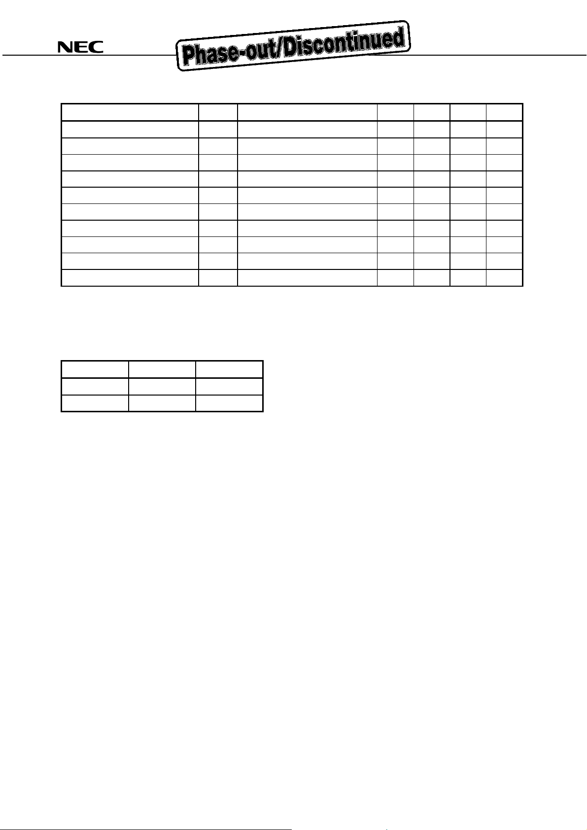
ELECTRICAL CHARACTERISTICS (TA = +25°°°°C)
Parameter Symbol Test Conditions MIN. TYP. MAX. Unit
2SC5437
Collector Cut-off Current I
Emitter Cut-off Current I
DC Current Gain
Gain Bandwidth Product (1) f
Gain Bandwidth Product (2) f
Insertion Power Gain (1)
Insertion Power Gain (2)
CBO
VCB = 5 V, IE = 0 mA – – 100 nA
EBO
VEB = 1 V, IC = 0 mA – – 100 nA
Note 1
FE
h
VCE = 1 V, IC = 3 mA 80 – 145 –
T
VCE = 1 V, IC = 3 mA, f = 2 GHz 4.0 5.0 – GHz
T
VCE = 3 V, IC = 20 mA, f = 2 GHz – 9.5 – GHz
2
21e
S
VCE = 1 V, IC = 3 mA, f = 2 GHz 3.0 4.0 – dB
2
21e
S
VCE = 3 V, IC = 20 mA, f = 2 GHz – 8.0 – dB
Noise Figure (1) NF VCE = 1 V, IC = 3 mA, f = 2 GHz – 1.9 2.5 dB
Noise Figure (2) NF VCE = 3 V, IC = 7 mA, f = 2 GHz – 1.7 – dB
Note 2
re
Reverse Transfer Capacitance
Notes 1.
Pulse measurement: PW ≤ 350
Collector to base capacitance when the emitter grounded
2.
C
VCB = 1 V, IE = 0 mA, f = 1 MHz – 0.7 0.8 pF
s, Duty Cycle ≤ 2%
µ
hFE CLASSIFICATION
Rank EB FB
Marking TS TT
hFE Value 80 to 110 100 to 145
2
Data Sheet PU10105EJ01V0DS
Page 5
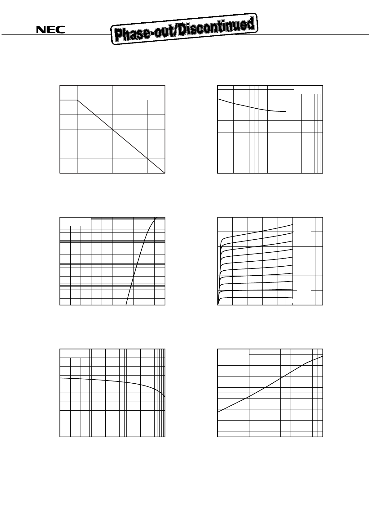
TYPICAL CHARACTERISTICS (Unless otherwise specified, TA = +25°°°°C)
2SC5437
TOTAL POWER DISSIPATION
vs. AMBIENT TEMPERATURE
150
125
(mW)
tot
100
75
50
25
Total Power Dissipation P
0
50 7525 100 125 150
Ambient Temperature TA (˚C)
COLLECTOR CURRENT vs.
BASE TO EMITTER VOLTAGE
100
VCE = 1 V
10
(mA)
C
1
0.1
Collector Current I
0.01
Base to Emitter Voltage VBE (V)
Free Air
0.50 1.0
REVERSE TRANSFER CAPACITANCE
vs. COLLECTOR TO BASE VOLTAGE
1.0
(pF)
re
0.5
0.2
Reverse Transfer Capacitance C
0.1
1 10 100
Collector to Base Voltage VCB (V)
f = 1 MHz
COLLECTOR CURRENT vs.
COLLECTOR TO EMITTER VOLTAGE
30
µ
200 A
25
(mA)
C
20
15
10
Collector Current I
5
0 345612 7
Collector to Emitter Voltage VCE (V)
µ
180 A
µ
160 A
µ
140 A
µ
120 A
µ
100 A
µ
80 A
µ
60 A
µ
40 A
µ
IB = 20 A
DC CURRENT GAIN vs.
COLLECTOR CURRENT
200
VCE = 1 V
FE
100
DC Current Gain h
0
0.1 101 100
Collector Current IC (mA)
(GHz)
T
Gain Bandwidth Product f
Data Sheet PU10105EJ01V0DS
GAIN BANDWIDTH PRODUCT
vs. COLLECTOR CURRENT
8
CE
= 1 V
V
f = 2 GHz
7
6
5
4
3
2
1
0
25110
Collector Current IC (mA)
3
Page 6

2SC5437
INSERTION POWER GAIN, MAG
vs. FREQUENCY
30
25
(dB)
20
2
|
21e
15
MAG
10
2
|S
21e
5
0
Maximum Available Power Gain MAG (dB)
Insertion Power Gain |S
0.1 1.0 10.0
|
Frequency f (GHz)
VCE = 1 V
I
C
= 5 mA
NOISE FIGURE vs. COLLECTOR CURRENT
4
3
VCE = 1 V
f = 2 GHz
INSERTION POWER GAIN
vs. COLLECTOR CURRENT
6
VCE = 1 V
f = 2 GHz
5
(dB)
2
|
21e
4
3
2
1
Insertion Power Gain |S
0
12 510
Collector Current I
C
(mA)
2
1
Noise Figure NF (dB)
0
Remark
The graphs indicate nominal characteristics.
25110
Collector Current IC (mA)
4
Data Sheet PU10105EJ01V0DS
Page 7

S-PARAMETERS
VCE = 1 V, IC = 1 mA, ZO = 50
Frequency S
(GHz) MAG. ANG.
0.2
0.4
0.6
0.8
1.0
1.2
1.4
1.6
1.8
2.0
2.2
2.4
2.6
2.8
3.0
0.903
0.746
0.675
0.608
0.561
0.541
0.539
0.525
0.510
0.523
0.548
0.562
0.573
0.584
0.605
11
Ω
(deg.)
−
35.0
−
66.3
−
93.2
−
112.2
−
128.6
−
143.1
−
153.8
−
162.9
−
173.3
176.9
170.0
164.7
159.6
154.7
150.7
21
S
MAG. ANG.
(deg.)
3.343
2.695
2.223
1.934
1.661
1.432
1.283
1.168
1.041
0.938
0.869
0.825
0.774
0.702
0.656
151.0
127.5
108.3
94.8
84.9
75.1
66.2
59.9
53.8
47.9
40.8
35.6
32.7
29.4
24.5
12
S
MAG. ANG.
(deg.)
0.092
0.155
0.189
0.200
0.207
0.209
0.203
0.191
0.175
0.165
0.159
0.154
0.150
0.151
0.153
66.0
46.6
33.9
24.4
17.1
13.0
12.1
11.5
10.6
9.4
11.7
16.0
21.5
27.9
32.5
2SC5437
22
S
MAG. ANG.
(deg.)
−
−
−
−
−
−
−
−
−
−
−
−
109.5
−
117.6
−
124.6
−
132.2
18.2
32.4
45.0
53.4
58.4
62.9
68.7
75.7
82.6
89.8
99.0
0.939
0.781
0.662
0.600
0.553
0.510
0.473
0.451
0.443
0.431
0.420
0.432
0.457
0.467
0.468
VCE = 1 V, IC = 3 mA, ZO = 50
Frequency S
(GHz) MAG. ANG.
0.2
0.4
0.6
0.8
1.0
1.2
1.4
1.6
1.8
2.0
2.2
2.4
2.6
2.8
3.0
0.748
0.584
0.526
0.486
0.469
0.477
0.483
0.473
0.473
0.494
0.516
0.530
0.542
0.556
0.575
11
VCE = 1 V, IC = 5 mA, ZO = 50
Frequency S
(GHz) MAG. ANG.
0.2
0.4
0.6
0.8
1.0
1.2
1.4
1.6
1.8
2.0
2.2
2.4
2.6
2.8
3.0
0.598
0.430
0.375
0.347
0.340
0.351
0.358
0.356
0.362
0.383
0.404
0.421
0.435
0.452
0.472
11
Ω
(deg.)
−
56.1
−
97.0
−
123.2
−
141.4
−
156.1
−
167.1
−
174.4
178.3
169.6
162.6
157.7
153.7
149.7
146.0
143.3
Ω
(deg.)
−
68.1
−
109.0
−
132.9
−
150.0
−
163.6
−
173.4
−
179.8
173.5
165.7
159.3
155.2
151.7
148.1
144.8
142.5
21
S
MAG. ANG.
(deg.)
7.879
5.518
4.133
3.325
2.790
2.327
2.050
1.832
1.617
1.447
1.325
1.255
1.184
1.085
1.005
139.2
114.6
98.1
88.3
81.2
74.1
67.2
62.4
57.8
52.8
46.8
42.0
39.1
36.5
31.7
21
S
MAG. ANG.
(deg.)
10.072
6.323
4.527
3.563
2.965
2.454
2.157
1.927
1.699
1.524
1.397
1.321
1.256
1.159
1.072
129.5
106.6
93.0
85.1
79.6
73.8
68.0
64.0
60.1
55.8
50.4
46.0
43.5
41.2
37.1
12
S
MAG. ANG.
(deg.)
0.080
0.114
0.129
0.135
0.141
0.148
0.155
0.157
0.160
0.164
0.174
0.185
0.197
0.205
0.210
56.6
40.2
33.4
30.0
28.6
28.9
31.6
34.6
36.3
36.2
36.6
37.6
39.6
41.2
41.6
12
S
MAG. ANG.
(deg.)
0.066
0.086
0.097
0.105
0.114
0.126
0.138
0.146
0.153
0.162
0.174
0.189
0.204
0.214
0.220
50.2
39.1
37.2
37.2
38.8
40.4
42.9
45.9
47.5
46.9
45.9
45.6
46.7
47.4
46.9
22
S
MAG. ANG.
(deg.)
−
0.811
0.552
0.420
0.346
0.292
0.255
0.235
0.223
0.218
0.212
0.221
0.242
0.261
0.277
0.289
35.7
−
58.2
−
73.5
−
82.6
−
89.6
−
97.0
−
105.6
−
114.0
−
122.0
−
131.8
−
142.3
−
150.4
−
155.7
−
161.8
−
167.8
22
S
MAG. ANG.
(deg.)
−
−
−
−
107.0
−
118.5
−
129.8
−
139.5
−
147.9
−
156.7
−
166.0
−
173.4
−
178.0
178.3
173.9
169.6
50.7
77.9
95.4
0.684
0.419
0.311
0.251
0.214
0.195
0.190
0.190
0.190
0.197
0.216
0.236
0.255
0.271
0.287
Data Sheet PU10105EJ01V0DS
5
Page 8

2SC5437
VCE = 1 V, IC = 7 mA, ZO = 50
Frequency S
(GHz) MAG. ANG.
0.2
0.4
0.6
0.8
1.0
1.2
1.4
1.6
1.8
2.0
2.2
2.4
2.6
2.8
3.0
0.561
0.469
0.444
0.432
0.438
0.456
0.462
0.457
0.463
0.487
0.506
0.520
0.533
0.548
0.566
11
VCE = 1 V, IC = 10 mA, ZO = 50
Frequency S
(GHz) MAG. ANG.
0.2
0.4
0.6
0.8
1.0
1.2
1.4
1.6
1.8
2.0
2.2
2.4
2.6
2.8
3.0
0.496
0.439
0.425
0.420
0.432
0.451
0.456
0.452
0.460
0.484
0.503
0.517
0.530
0.545
0.563
11
Ω
(deg.)
−
85.4
−
128.0
−
149.4
−
164.1
−
175.2
177.5
172.7
166.8
159.6
154.2
150.6
147.3
143.8
140.8
138.8
Ω
(deg.)
−
99.1
−
139.2
−
158.0
−
171.0
179.3
173.3
169.1
163.6
157.0
152.1
148.8
145.6
142.4
139.5
137.6
21
S
MAG. ANG.
(deg.)
12.549
7.589
5.337
4.184
3.455
2.933
2.503
2.226
1.953
1.744
1.589
1.499
1.420
1.305
1.202
125.2
103.4
90.6
83.5
78.0
72.0
66.6
62.8
58.9
54.6
49.4
45.1
42.6
40.4
36.2
21
S
MAG. ANG.
(deg.)
14.099
8.130
5.656
4.400
3.622
3.070
2.622
2.325
2.036
1.818
1.656
1.560
1.476
1.360
1.250
120.4
99.5
88.4
82.0
77.1
71.6
66.4
62.9
59.2
55.2
50.1
46.1
43.6
41.5
37.5
12
S
MAG. ANG.
(deg.)
0.060
0.079
0.092
0.103
0.115
0.130
0.146
0.158
0.168
0.179
0.193
0.209
0.226
0.237
0.242
50.5
41.8
42.3
43.9
45.5
46.7
48.4
50.1
50.8
49.6
47.9
46.6
46.9
47.0
45.7
12
S
MAG. ANG.
(deg.)
0.051
0.067
0.083
0.097
0.112
0.128
0.146
0.161
0.172
0.185
0.199
0.216
0.234
0.245
0.251
48.8
44.9
48.0
50.1
51.7
52.4
53.3
54.3
54.4
52.8
50.5
49.0
48.7
48.4
47.1
22
S
MAG. ANG.
(deg.)
−
0.627
0.381
0.290
0.242
0.216
0.209
0.211
0.213
0.217
0.228
0.249
0.269
0.286
0.302
0.319
59.0
−
89.6
−
109.0
−
123.1
−
136.1
−
147.8
−
156.1
−
163.6
−
171.8
−
179.9
174.3
170.6
167.5
163.4
160.1
22
S
MAG. ANG.
(deg.)
−
−
103.3
−
123.9
−
138.8
−
152.2
−
162.4
−
169.0
−
175.5
177.1
170.2
165.6
162.7
159.8
156.4
153.4
69.8
0.555
0.340
0.270
0.238
0.224
0.227
0.234
0.237
0.243
0.257
0.279
0.297
0.312
0.329
0.346
VCE = 3 V, IC = 1 mA, ZO = 50
Frequency S
(GHz) MAG. ANG.
0.2
0.4
0.6
0.8
1.0
1.2
1.4
1.6
1.8
2.0
2.2
2.4
2.6
2.8
3.0
0.922
0.781
0.711
0.645
0.594
0.564
0.557
0.541
0.520
0.530
0.553
0.567
0.576
0.586
0.605
11
6
Ω
(deg.)
−
31.0
−
59.5
−
85.9
−
104.8
−
121.1
−
136.2
−
147.7
−
157.3
−
168.1
−
178.5
173.7
168.1
162.8
157.6
153.2
21
S
MAG. ANG.
(deg.)
3.396
2.823
2.381
2.107
1.841
1.591
1.424
1.299
1.165
1.050
0.969
0.922
0.870
0.792
0.738
Data Sheet PU10105EJ01V0DS
154.4
132.8
114.4
100.9
91.1
81.8
72.6
66.1
60.1
54.3
47.2
41.7
38.6
35.1
30.1
12
S
MAG. ANG.
(deg.)
0.072
0.122
0.154
0.166
0.173
0.176
0.171
0.162
0.149
0.140
0.136
0.133
0.134
0.138
0.143
68.3
51.1
39.1
29.5
22.3
18.1
17.7
17.5
17.5
17.1
20.0
25.2
31.9
38.9
44.2
22
S
MAG. ANG.
(deg.)
−
−
−
−
−
−
−
−
−
−
−
−
−
−
105.9
−
112.8
14.0
25.2
35.9
43.6
47.9
51.2
55.6
61.3
67.6
73.8
81.0
90.7
99.1
0.959
0.833
0.724
0.670
0.634
0.593
0.553
0.523
0.511
0.500
0.482
0.479
0.497
0.505
0.497
Page 9

2SC5437
VCE = 3 V, IC = 3 mA, ZO = 50
Frequency S
(GHz) MAG. ANG.
0.2
0.4
0.6
0.8
1.0
1.2
1.4
1.6
1.8
2.0
2.2
2.4
2.6
2.8
3.0
0.782
0.605
0.536
0.481
0.453
0.452
0.456
0.446
0.442
0.461
0.484
0.499
0.511
0.526
0.545
11
VCE = 3 V, IC = 5 mA, ZO = 50
Frequency S
(GHz) MAG. ANG.
0.2
0.4
0.6
0.8
1.0
1.2
1.4
1.6
1.8
2.0
2.2
2.4
2.6
2.8
3.0
0.677
0.512
0.456
0.420
0.408
0.416
0.424
0.418
0.419
0.440
0.463
0.479
0.492
0.508
0.527
11
Ω
(deg.)
−
47.6
−
85.1
−
111.7
−
130.4
−
145.8
−
158.4
−
166.9
−
174.8
176.0
168.0
162.5
158.2
154.0
150.0
146.9
Ω
(deg.)
−
59.7
−
100.5
−
125.9
−
143.6
−
157.9
−
168.5
−
175.3
177.7
169.4
162.7
158.1
154.3
150.4
146.9
144.4
21
S
MAG. ANG.
(deg.)
8.239
6.070
4.667
3.796
3.207
2.689
2.366
2.123
1.879
1.682
1.536
1.451
1.376
1.261
1.167
143.8
120.0
103.1
92.9
85.7
78.8
71.7
66.8
62.2
57.3
51.3
46.3
43.4
40.4
35.8
21
S
MAG. ANG.
(deg.)
11.364
7.682
5.639
4.496
3.744
3.206
2.769
2.440
2.151
1.921
1.752
1.651
1.566
1.438
1.327
136.5
112.9
98.0
89.3
83.3
77.0
70.6
66.5
62.5
58.0
52.6
47.9
45.2
42.6
38.2
12
S
MAG. ANG.
(deg.)
0.062
0.093
0.109
0.115
0.122
0.128
0.135
0.138
0.141
0.146
0.154
0.166
0.180
0.190
0.195
61.0
45.1
38.0
34.5
33.2
33.8
36.2
39.7
42.0
42.3
43.1
44.3
46.2
48.5
49.0
12
S
MAG. ANG.
(deg.)
0.056
0.078
0.091
0.099
0.108
0.118
0.130
0.138
0.146
0.154
0.166
0.180
0.197
0.208
0.214
57.6
44.3
41.5
41.0
42.3
43.5
45.9
48.6
50.5
50.0
49.3
49.0
50.0
50.7
50.3
22
S
MAG. ANG.
(deg.)
−
0.860
0.625
0.488
0.416
0.360
0.319
0.286
0.262
0.249
0.236
0.226
0.231
0.244
0.251
0.255
27.1
−
44.1
−
55.9
−
62.2
−
65.6
−
68.8
−
73.8
−
80.0
−
86.3
−
93.4
−
102.9
−
113.6
−
121.5
−
128.7
−
136.2
22
S
MAG. ANG.
(deg.)
−
−
−
−
−
−
−
−
−
107.7
−
117.8
−
129.2
−
139.8
−
146.4
−
153.9
−
160.9
36.3
56.0
68.2
74.9
79.3
84.4
91.6
99.6
0.776
0.508
0.378
0.309
0.257
0.220
0.195
0.178
0.169
0.159
0.160
0.173
0.187
0.200
0.209
VCE = 3 V, IC = 7 mA, ZO = 50
Frequency S
(GHz) MAG. ANG.
0.2
0.4
0.6
0.8
1.0
1.2
1.4
1.6
1.8
2.0
2.2
2.4
2.6
2.8
3.0
0.587
0.450
0.408
0.386
0.384
0.397
0.406
0.401
0.408
0.430
0.451
0.468
0.482
0.498
0.517
11
Ω
(deg.)
−
70.9
−
113.1
−
136.9
−
153.3
−
166.2
−
175.1
179.1
172.8
165.2
159.1
155.1
151.8
148.1
144.9
142.6
21
S
MAG. ANG.
(deg.)
13.785
8.717
6.260
4.926
4.074
3.474
3.002
2.613
2.320
2.074
1.888
1.775
1.683
1.547
1.422
Data Sheet PU10105EJ01V0DS
131.0
107.8
94.6
86.9
81.6
75.8
70.1
66.0
62.5
58.4
53.2
48.8
46.1
43.9
39.7
12
S
MAG. ANG.
(deg.)
0.049
0.067
0.080
0.090
0.102
0.115
0.129
0.141
0.151
0.162
0.175
0.190
0.207
0.219
0.225
54.4
46.4
46.4
47.1
49.2
50.6
52.2
54.0
55.3
54.2
52.9
51.7
51.9
52.4
51.4
22
S
MAG. ANG.
(deg.)
−
−
−
−
−
−
102.2
−
111.9
−
121.8
−
131.5
−
143.3
−
154.7
−
162.7
−
167.8
−
173.8
−
179.4
44.5
66.1
79.3
87.2
94.2
0.696
0.425
0.308
0.245
0.200
0.171
0.154
0.144
0.141
0.140
0.149
0.167
0.183
0.197
0.212
7
Page 10

2SC5437
VCE = 3 V, IC = 10 mA, ZO = 50
Frequency S
(GHz) MAG. ANG.
0.2
0.4
0.6
0.8
1.0
1.2
1.4
1.6
1.8
2.0
2.2
2.4
2.6
2.8
3.0
0.507
0.404
0.377
0.364
0.370
0.386
0.394
0.392
0.400
0.423
0.444
0.461
0.475
0.492
0.512
11
Ω
(deg.)
−
82.3
−
124.5
−
146.4
−
161.3
−
172.7
179.7
174.9
169.0
162.1
156.6
153.0
149.8
146.3
143.4
141.3
21
S
MAG. ANG.
(deg.)
15.830
9.537
6.711
5.250
4.334
3.675
3.173
2.757
2.446
2.183
1.984
1.865
1.769
1.630
1.499
125.7
103.9
92.0
85.2
80.4
75.0
69.7
65.9
62.6
58.7
53.8
49.6
47.1
44.9
41.0
12
S
MAG. ANG.
(deg.)
0.044
0.059
0.073
0.086
0.100
0.114
0.130
0.144
0.156
0.168
0.181
0.198
0.216
0.228
0.234
54.4
48.9
51.3
53.1
55.0
55.6
56.7
58.0
58.5
57.1
54.9
53.3
53.3
53.3
51.9
22
S
MAG. ANG.
(deg.)
−
−
−
−
100.5
−
110.3
−
121.9
−
132.5
−
142.3
−
152.6
−
163.7
−
172.3
−
177.7
178.2
173.4
168.9
52.5
75.9
90.6
0.619
0.361
0.259
0.204
0.169
0.148
0.141
0.140
0.140
0.146
0.162
0.181
0.200
0.214
0.231
8
Data Sheet PU10105EJ01V0DS
Page 11

PACKAGE DIMENSIONS
FLAT-LEAD 3-PIN THIN-TYPE ULTRA SUPER MINIMOLD (UNIT: mm)
1.2 ± 0.05
0.8 ± 0.1
2SC5437
(0.9)
1.4 ± 0.1
0.59 ± 0.05
+0.1
2
–0
0.2
1
0.450.45
PIN CONNECTIONS
1. Emitter
2. Base
3. Collector
T S
–0
+0.1
0.3
3
–0.05
+0.1
0.15
Data Sheet PU10105EJ01V0DS
9
Page 12

2SC5437
•
The information in this document is current as of February, 2002. The information is subject to
change without notice. For actual design-in, refer to the latest publications of NEC's data sheets or
data books, etc., for the most up-to-date specifications of NEC semiconductor products. Not all
products and/or types are available in every country. Please check with an NEC sales representative
for availability and additional information.
•
No part of this document may be copied or reproduced in any form or by any means without prior
written consent of NEC. NEC assumes no responsibility for any errors that may appear in this document.
•
NEC does not assume any liability for infringement of patents, copyrights or other intellectual property rights of
third parties by or arising from the use of NEC semiconductor products listed in this document or any other
liability arising from the use of such products. No license, express, implied or otherwise, is granted under any
patents, copyrights or other intellectual property rights of NEC or others.
•
Descriptions of circuits, software and other related information in this document are provided for illustrative
purposes in semiconductor product operation and application examples. The incorporation of these
circuits, software and information in the design of customer's equipment shall be done under the full
responsibility of customer. NEC assumes no responsibility for any losses incurred by customers or third
parties arising from the use of these circuits, software and information.
•
While NEC endeavours to enhance the quality, reliability and safety of NEC semiconductor products, customers
agree and acknowledge that the possibility of defects thereof cannot be eliminated entirely. To minimize
risks of damage to property or injury (including death) to persons arising from defects in NEC
semiconductor products, customers must incorporate sufficient safety measures in their design, such as
redundancy, fire-containment, and anti-failure features.
•
NEC semiconductor products are classified into the following three quality grades:
"Standard", "Special" and "Specific". The "Specific" quality grade applies only to semiconductor products
developed based on a customer-designated "quality assurance program" for a specific application. The
recommended applications of a semiconductor product depend on its quality grade, as indicated below.
Customers must check the quality grade of each semiconductor product before using it in a particular
application.
"Standard": Computers, office equipment, communications equipment, test and measurement equipment, audio
and visual equipment, home electronic appliances, machine tools, personal electronic equipment
and industrial robots
"Special": Transportation equipment (automobiles, trains, ships, etc.), traffic control systems, anti-disaster
systems, anti-crime systems, safety equipment and medical equipment (not specifically designed
for life support)
"Specific": Aircraft, aerospace equipment, submersible repeaters, nuclear reactor control systems, life
support systems and medical equipment for life support, etc.
The quality grade of NEC semiconductor products is "Standard" unless otherwise expressly specified in NEC's
data sheets or data books, etc. If customers wish to use NEC semiconductor products in applications not
intended by NEC, they must contact an NEC sales representative in advance to determine NEC's willingness
to support a given application.
(Note)
(1) "NEC" as used in this statement means NEC Corporation, NEC Compound Semiconductor Devices, Ltd.
and also includes its majority-owned subsidiaries.
(2) "NEC semiconductor products" means any semiconductor product developed or manufactured by or for
NEC (as defined above).
M8E 00. 4 - 0110
10
Data Sheet PU10105EJ01V0DS
Page 13

2SC5437
Business issue
NEC Compound Semiconductor Devices, Ltd.
5th Sales Group, Sales Division TEL: +81-3-3798-6372 FAX: +81-3-3798-6783 E-mail: salesinfo@csd-nec.com
NEC Compound Semiconductor Devices Hong Kong Limited
Hong Kong Head Office
Taipei Branch Office
Korea Branch Office
NEC Electron Devices European Operations http://www.nec.de/
TEL: +49-211-6503-101 FAX: +49-211-6503-487
California Eastern Laboratories, Inc. http://www.cel.com/
TEL: +1-408-988-3500 FAX: +1-408-988-0279
Technical issue
NEC Compound Semiconductor Devices, Ltd. http://www.csd-nec.com/
Sales Engineering Group, Sales Division
E-mail: techinfo@csd-nec.com FAX: +81-44-435-1918
TEL: +852-3107-7303
TEL: +886-2-8712-0478
TEL: +82-2-528-0301
FAX: +852-3107-7309
FAX: +886-2-2545-3859
FAX: +82-2-528-0302
0110
Page 14

 Loading...