

Page 1
1
Motorola Bipolar Power Transistor Device Data
The 2N6547 transistor is designed for high–voltage, high–speed, power switching
in inductive circuits where fall time is critical. They are particularly suited for 115 and
220 volt line operated switch–mode applications such as:
• Switching Regulators
• PWM Inverters and Motor Controls
• Solenoid and Relay Drivers
• Deflection Circuits
Specification Features —
High Temperature Performance Specified for:
Reversed Biased SOA with Inductive Loads
Switching Times with Inductive Loads
Saturation Voltages
Leakage Currents
MAXIMUM RATINGS (1)
Rating
Symbol
ОООООООО
ОООООООО
ОООООООО
Value
ÎÎÎÎ
ÎÎÎÎ
ÎÎÎÎ
Unit
Collector–Emitter Voltage
V
CEO(sus)
ОООООООО
ОООООООО
ОООООООО
400
ÎÎÎÎ
ÎÎÎÎ
ÎÎÎÎ
Vdc
Collector–Emitter Voltage
V
CEX(sus)
ОООООООО
ОООООООО
ОООООООО
450
ÎÎÎÎ
ÎÎÎÎ
ÎÎÎÎ
Vdc
Collector–Emitter Voltage
V
CEV
ОООООООО
ОООООООО
ОООООООО
850
ÎÎÎÎ
ÎÎÎÎ
ÎÎÎÎ
Vdc
Emitter Base Voltage
V
EB
ОООООООО
ОООООООО
ОООООООО
9.0
ÎÎÎÎ
ÎÎÎÎ
ÎÎÎÎ
Vdc
Collector Current— Continuous
— Peak (2)
I
C
I
CM
ОООООООО
ОООООООО
ОООООООО
ОООООООО
15
30
ÎÎÎÎ
ÎÎÎÎ
ÎÎÎÎ
ÎÎÎÎ
Adc
Base Current — Continuous
— Peak (2)
I
B
I
BM
ОООООООО
ОООООООО
ОООООООО
10
20
ÎÎÎÎ
ÎÎÎÎ
ÎÎÎÎ
Adc
Emitter Current— Continuous
— Peak (2)
I
E
I
EM
ОООООООО
ОООООООО
ОООООООО
ОООООООО
25
35
ÎÎÎÎ
ÎÎÎÎ
ÎÎÎÎ
ÎÎÎÎ
Adc
Total Power Dissipation
@ TC = 25_C
@ TC = 100_C
Derate above 25_C
P
D
ОООООООО
ОООООООО
ОООООООО
ОООООООО
ОООООООО
175
100
1.0
ÎÎÎÎ
ÎÎÎÎ
ÎÎÎÎ
ÎÎÎÎ
ÎÎÎÎ
Watts
W/_C
Operating and Storage Junction Temperature Range
TJ, T
stg
ОООООООО
ОООООООО
ОООООООО
–65 to +200
ÎÎÎÎ
ÎÎÎÎ
ÎÎÎÎ
_
C
THERMAL CHARACTERISTICS
Characteristic
Symbol
ОООООООО
ОООООООО
ОООООООО
Max
ÎÎÎÎ
ÎÎÎÎ
ÎÎÎÎ
Unit
Thermal Resistance, Junction to Case
R
θJC
ОООООООО
ОООООООО
ОООООООО
1.0
ÎÎÎÎ
ÎÎÎÎ
ÎÎÎÎ
_
C/W
Maximum Lead Temperature for Soldering
Purposes: 1/8″ from Case for 5 Seconds
T
L
ОООООООО
ОООООООО
ОООООООО
ОООООООО
275
ÎÎÎÎ
ÎÎÎÎ
ÎÎÎÎ
ÎÎÎÎ
_
C
Designer’s and SWITCHMODE are trademarks of Motorola, Inc.
Designer’s Data for “Worst Case” Conditions — The Designer’s Data Sheet permits the design of most circuits entirely from the information presented. SOA Limit
curves — representing boundaries on device characteristics — are given to facilitate “worst case” design.
SEMICONDUCTOR TECHNICAL DATA
Order this document
by 2N6547/D
Motorola, Inc. 1995
15 AMPERE
NPN SILICON
POWER TRANSISTORS
300 and 400 VOLTS
175 WATTS
CASE 1–07
TO–204AA
(TO–3)
REV 4
Page 2
2N6547
2
Motorola Bipolar Power Transistor Device Data
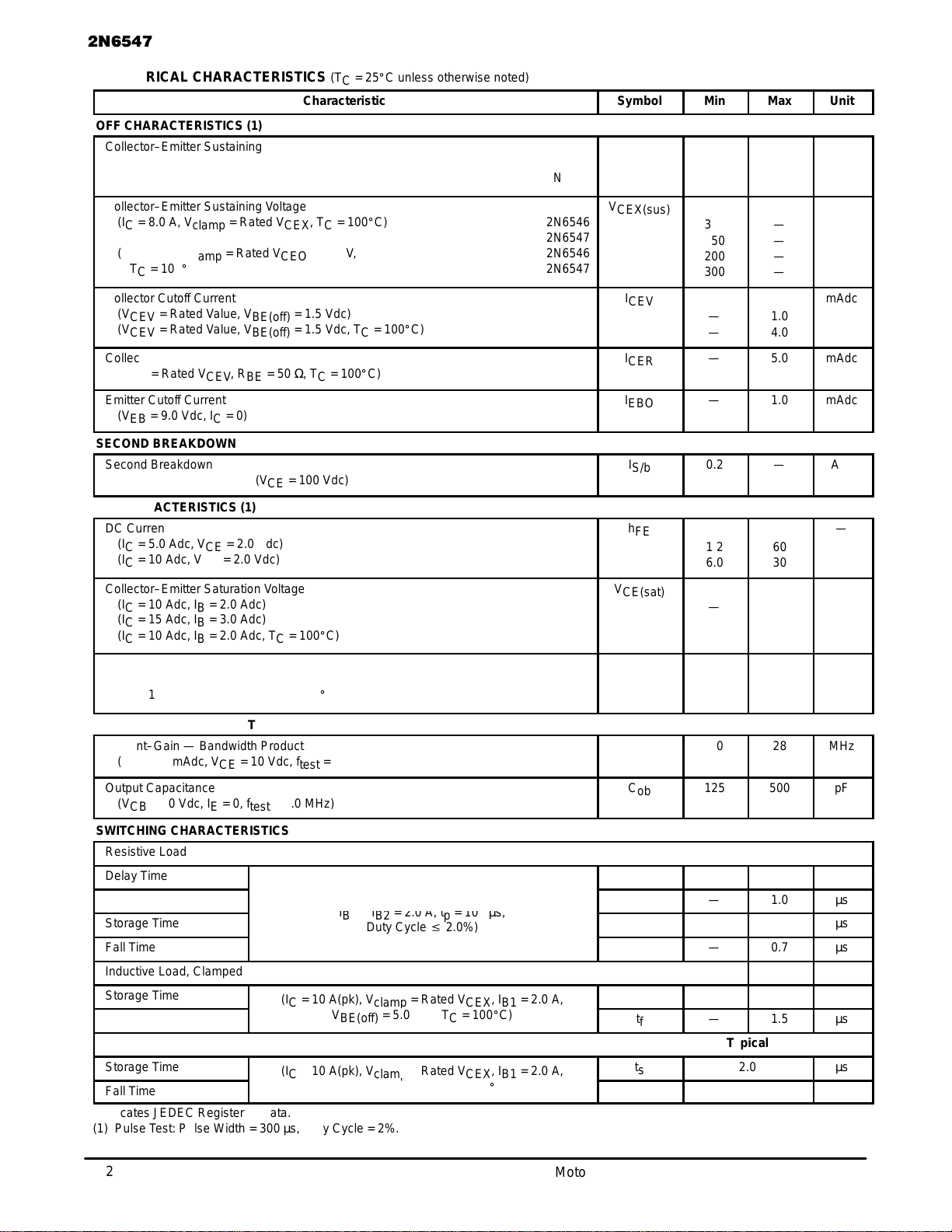
*ELECTRICAL CHARACTERISTICS (T
C
= 25_C unless otherwise noted)
Characteristic
ÎÎÎÎ
ÎÎÎÎ
ÎÎÎÎ
Symbol
Min
Max
ÎÎÎ
ÎÎÎ
ÎÎÎ
Unit
OFF CHARACTERISTICS (1)
Collector–Emitter Sustaining Voltage
(IC = 100 mA, IB = 0) 2N6546
2N6547
ÎÎÎÎ
ÎÎÎÎ
ÎÎÎÎ
ÎÎÎÎ
ÎÎÎÎ
V
CEO(sus)
300
400
—
—
ÎÎÎ
ÎÎÎ
ÎÎÎ
ÎÎÎ
ÎÎÎ
Vdc
Collector–Emitter Sustaining Voltage
(IC = 8.0 A, V
clamp
= Rated V
CEX
, TC = 100_C) 2N6546
2N6547
(IC = 15 A, V
clamp
= Rated V
CEO
= 100 V, 2N6546
TC = 100_C) 2N6547
ÎÎÎÎ
ÎÎÎÎ
ÎÎÎÎ
ÎÎÎÎ
ÎÎÎÎ
ÎÎÎÎ
V
CEX(sus)
350
450
200
300
—
—
—
—
ÎÎÎ
ÎÎÎ
ÎÎÎ
ÎÎÎ
ÎÎÎ
ÎÎÎ
Vdc
Collector Cutoff Current
(V
CEV
= Rated Value, V
BE(off)
= 1.5 Vdc)
(V
CEV
= Rated Value, V
BE(off)
= 1.5 Vdc, TC = 100_C)
ÎÎÎÎ
ÎÎÎÎ
ÎÎÎÎ
ÎÎÎÎ
I
CEV
—
—
1.0
4.0
ÎÎÎ
ÎÎÎ
ÎÎÎ
ÎÎÎ
mAdc
Collector Cutoff Current
(VCE = Rated V
CEV
, RBE = 50 Ω, TC = 100_C)
ÎÎÎÎ
ÎÎÎÎ
ÎÎÎÎ
ÎÎÎÎ
I
CER
—
5.0
ÎÎÎ
ÎÎÎ
ÎÎÎ
ÎÎÎ
mAdc
Emitter Cutoff Current
(VEB = 9.0 Vdc, IC = 0)
ÎÎÎÎ
ÎÎÎÎ
ÎÎÎÎ
ÎÎÎÎ
I
EBO
—
1.0
ÎÎÎ
ÎÎÎ
ÎÎÎ
ÎÎÎ
mAdc
SECOND BREAKDOWN
Second Breakdown Collector Current with base forward biased
t = 1.0 s (non–repetitive) (VCE = 100 Vdc)
ÎÎÎÎ
ÎÎÎÎ
ÎÎÎÎ
I
S/b
0.2
—
ÎÎÎ
ÎÎÎ
ÎÎÎ
Adc
ON CHARACTERISTICS (1)
DC Current Gain
(IC = 5.0 Adc, VCE = 2.0 Vdc)
(IC = 10 Adc, VCE = 2.0 Vdc)
ÎÎÎÎ
ÎÎÎÎ
ÎÎÎÎ
ÎÎÎÎ
ÎÎÎÎ
h
FE
1 2
6.0
60
30
ÎÎÎ
ÎÎÎ
ÎÎÎ
ÎÎÎ
ÎÎÎ
—
Collector–Emitter Saturation Voltage
(IC = 10 Adc, IB = 2.0 Adc)
(IC = 15 Adc, IB = 3.0 Adc)
(IC = 10 Adc, IB = 2.0 Adc, TC = 100_C)
ÎÎÎÎ
ÎÎÎÎ
ÎÎÎÎ
ÎÎÎÎ
ÎÎÎÎ
V
CE(sat)
—
—
—
1.5
5.0
2.5
ÎÎÎ
ÎÎÎ
ÎÎÎ
ÎÎÎ
ÎÎÎ
Vdc
Base–Emitter Saturation Voltage
(IC = 10 Adc, IB = 2.0 Adc)
(IC = 10 Adc, IB = 2.0 Adc, TC = 100_C
ÎÎÎÎ
ÎÎÎÎ
ÎÎÎÎ
ÎÎÎÎ
V
BE(sat)
—
—
1.6
1.6
ÎÎÎ
ÎÎÎ
ÎÎÎ
ÎÎÎ
Vdc
DYNAMIC CHARACTERISTICS
Current–Gain — Bandwidth Product
(IC = 500 mAdc, VCE = 10 Vdc, f
test
= 1.0 MHz)
ÎÎÎÎ
ÎÎÎÎ
ÎÎÎÎ
ÎÎÎÎ
f
T
6.0
28
ÎÎÎ
ÎÎÎ
ÎÎÎ
ÎÎÎ
MHz
Output Capacitance
(VCB = 10 Vdc, IE = 0, f
test
= 1.0 MHz)
ÎÎÎÎ
ÎÎÎÎ
ÎÎÎÎ
ÎÎÎÎ
C
ob
125
500
ÎÎÎ
ÎÎÎ
ÎÎÎ
ÎÎÎ
pF
SWITCHING CHARACTERISTICS
Resistive Load
Delay Time
ÎÎÎÎ
ÎÎÎÎ
ÎÎÎÎ
t
d
—
0.05
ÎÎÎ
ÎÎÎ
ÎÎÎ
µs
Rise Time
ÎÎÎÎ
ÎÎÎÎ
ÎÎÎÎ
t
r
—
1.0
ÎÎÎ
ÎÎÎ
ÎÎÎ
µs
Storage Time
IB1 = IB2 = 2.0 A, tp = 100 µs,
Duty Cycle v 2.0%)
ÎÎÎÎ
ÎÎÎÎ
ÎÎÎÎ
t
s
—
4.0
ÎÎÎ
ÎÎÎ
ÎÎÎ
µs
Fall Time
v
2.0%)
ÎÎÎÎ
ÎÎÎÎ
ÎÎÎÎ
t
f
—
0.7
ÎÎÎ
ÎÎÎ
ÎÎÎ
µs
Inductive Load, Clamped
ÎÎÎ
ÎÎÎ
ÎÎÎ
Storage Time
C
= 10 A(pk), V
clamp
= Rated V
CEX
, IB1 = 2.0 A,
ÎÎÎÎ
ÎÎÎÎ
ÎÎÎÎ
t
s
—
5.0
ÎÎÎ
ÎÎÎ
ÎÎÎ
µs
Fall Time
(IC = 10 A(pk), V
clamp
= Rated V
CEX
, IB1 = 2.0 A,
V
BE(off)
= 5.0 Vdc, TC = 100_C)
ÎÎÎÎ
ÎÎÎÎ
ÎÎÎÎ
t
f
—
1.5
ÎÎÎ
ÎÎÎ
ÎÎÎ
µs
ÎÎÎÎ
ÎÎÎÎ
ÎÎÎÎ
Typical
ÎÎÎ
ÎÎÎ
ÎÎÎ
Storage Time
C
= 10 A(pk), V
clamp
= Rated V
CEX
, IB1 = 2.0 A,
ÎÎÎÎ
ÎÎÎÎ
ÎÎÎÎ
t
s
2.0
ÎÎÎ
ÎÎÎ
ÎÎÎ
µs
Fall Time
(IC = 10 A(pk), V
clamp
= Rated V
CEX
, IB1 = 2.0 A,
V
BE(off)
= 5.0 Vdc, TC = 25_C)
ÎÎÎÎ
ÎÎÎÎ
ÎÎÎÎ
t
f
0.09
ÎÎÎ
ÎÎÎ
ÎÎÎ
µs
*Indicates JEDEC Registered Data.
(1) Pulse Test: Pulse Width = 300 µs, Duty Cycle = 2%.
(VCC = 250 V, IC = 10 A,
(I
(I
Page 3
2N6547
3
Motorola Bipolar Power Transistor Device Data
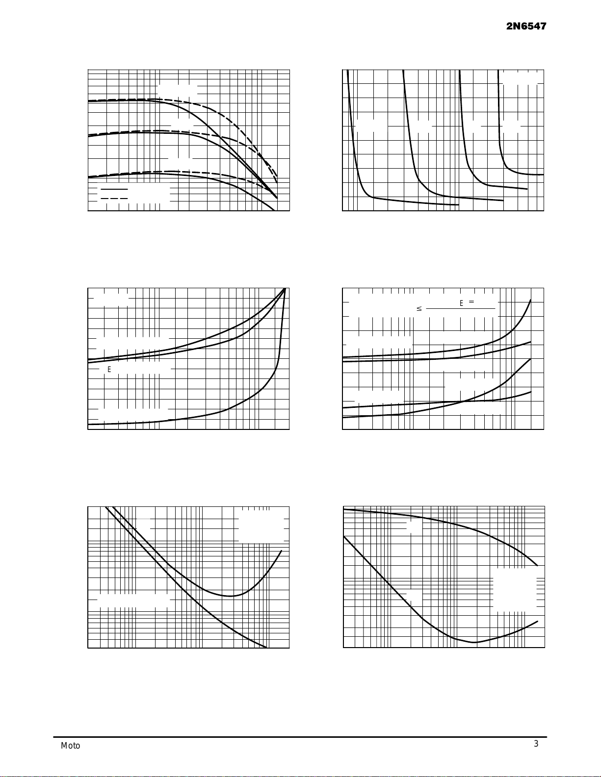
TYPICAL ELECTRICAL CHARACTERISTICS
TS)
100
Figure 1. DC Current Gain
IC, COLLECTOR CURRENT (AMP)
5.0
50
30
20
1.4
Figure 2. Collector Saturation Region
IC, COLLECTOR CURRENT (AMP)
1.0
0.6
0.4
0.2
0
TJ = 25°C
V
BE(sat)
@ IC/IB = 5.0
2.0
Figure 3. “On” Voltages
IB, COLLECTOR CURRENT (AMP)
0
0.07 0.2 0.3 0.5 1.0 7.0
1.6
70
h
FE
, DC CURRENT GAIN
TJ = 150°C
25°C
–55°C
TJ = 25°C
IC = 2.0 A
10 A
V, VOLTAGE (VOLTS)
2.5
Figure 4. Temperature Coefficients
IC, COLLECTOR CURRENT (AMP)
V
, TEMPERATURE COEFFICIENTS (mV/ C)
°θ
2.0
1.0
0
–2.5
θ
VB
for V
BE
*
θ
VC
for V
CE(sat)
*APPLIES FOR IC/IB
v
h
FE
@ V
CE
+
2.0 V
3
V
BE(on)
@ VCE = 2.0 V
1.2
0.8
0.1 0.7
1.2
0.8
0.4
1.5
–1.0
–1.5
10
7.0
0.2 0.3 1.0 2.0 3.0 20
5.0 A
2.0 5.0
V
CE(sat)
@ IC/IB = 5
0.2 0.3 1.0 7.00.5 2.0 3.0 20 0.5 1.0 2.0 3.0 100.7 7.05.0 20
0.3
0.2
–55°C to 25°C
25°C to 150°C
25°C to 150°C
VCE = 2.0 V
VCE = 10 V
0.5 5.0 7.0 10 3.0
15 A
0.5
5.0 10
–0.5
–2.0
–55°C to 25°C
3.0 k
Figure 5. Turn–On Time
IC, COLLECTOR CURRENT (AMP)
0.02 20
VCC = 250 V
IC/IB = 5.0
TJ = 25°C
1.00.1 2.0
t
r
td @ V
BE(off)
= 5.0 V
t, TIME (ns)
30
2.0 k
1.0 k
700
500
300
200
100
70
50
0.05 100.2 0.5
Figure 6. Turn–Off Time
IC, COLLECTOR CURRENT (AMP)
VCC = 250 V
IC/IB = 5.0
IB1 = I
B2
TJ = 25
°
C
t
s
t
f
10 k
7.0 k
5.0 k
3.0 k
2.0 k
1.0 k
700
500
100
300
200
t, TIME (ns)
5.0 0.02 201.00.1 2.00.05 100.2 0.5 5.0
, COLLECTOR–EMITTER VOLTAGE (VOL
CE
V
Page 4
2N6547
4
Motorola Bipolar Power Transistor Device Data
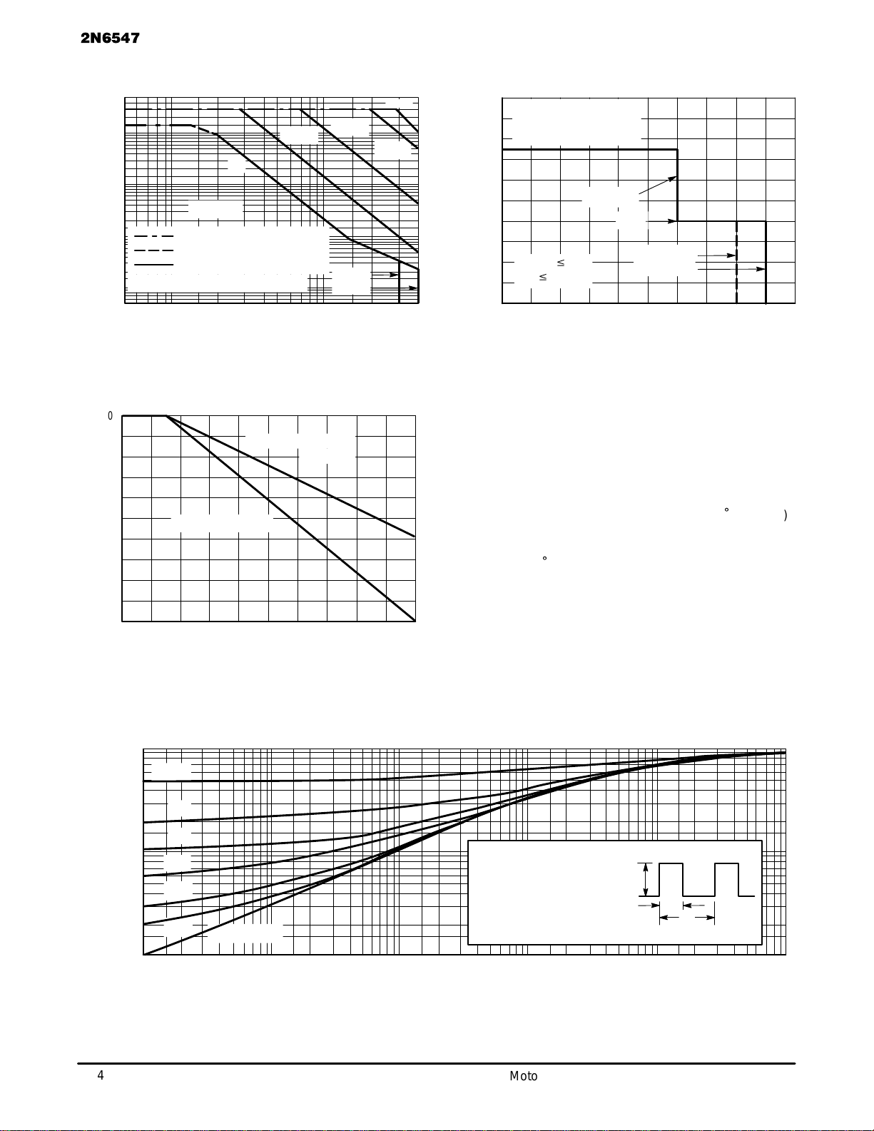
MAXIMUM RATED SAFE OPERATING AREAS
VCE, COLLECTOR–EMITTER VOLTAGE (VOLTS)
BONDING WIRE LIMITED
THERMAL LIMIT (SINGLE PULSE)
SECOND BREAKDOWN LIMIT
50
Figure 7. Forward Bias Safe Operating Area
5.0
10 20 400
TC = 25°C
0.2
10
0.5
20
70
1.0
0.005
dc
5.0 1007.0
2N6546
2N6547
CURVES APPLY BELOW RATED V
CEO
5.0 ms
1.0 ms
100 µs
I
C
, COLLECTOR CURRENT (AMP)
0.1
0.01
30 50 300200
0.02
0.05
2.0
10 ms
TURN OFF LOAD LINE
BOUNDARY FOR 2N6547.
FOR 2N6546, V
CEO
AND
V
CEX
ARE 100 VOLTS LESS.
20
Figure 8. Reverse Bias Safe Operating Area
100 500
V
CEX(sus)
8.0
16
VCE, COLLECTOR–EMITTER VOLTAGE (VOLTS)
12
0
0 400
V
CEO(sus)
V
CEX(sus)
8.0 V
I
C
, COLLECTOR CURRENT (AMP)
4.0
300200
V
BE(off)
v 5 V
TC
v
100°C
100
80
60
20
0
0 40 80 120 160 200
Figure 9. Power Derating
TC, CASE TEMPERATURE (°C)
POWER DERATING FACTOR (%)
THERMAL DERATING
40
SECOND BREAKDOWN
DERATING
There are two limitations on the power handling ability of a
transistor: average junction temperature and second breakdown. Safe operating area curves indicate IC – VCE limits of
the transistor that must be observed for reliable operation;
i.e., the transistor must not be subjected to greater dissipation than the curves indicate.
The data of Figure 7 is based on TC = 25_C; T
J(pk)
is
variable depending on power level. Second breakdown pulse
limits are valid for duty cycles to 10% but must be derated
when TC ≥ 25_C. Second breakdown limitations do not derate the same as thermal limitations. Allowable current at the
voltages shown on Figure 7 may be found at any case temperature by using the appropriate curve on Figure 9.
T
J(pk)
may be calculated from the data in Figure 10. At
high case temperatures, thermal limitations will reduce the
power that can be handled to values less than the limitations
imposed by second breakdown.
Figure 10. Thermal Response
t, TIME (ms)
1.0
0.01
0.01
0.7
0.5
0.3
0.2
0.1
0.07
0.05
0.03
0.02
0.02 0.05 0.1 0.2 0.5 1.0 2.0 5.0 10 20 50 100 200 1.0 k500
Z
θ
JC
(t) = r(t) R
θ
JC
R
θ
JC
= 1.0
°
C/W MAX
D CURVES APPLY FOR POWER
PULSE TRAIN SHOWN
READ TIME AT t
1
T
J(pk)
– TC = P
(pk)
Z
θ
JC(t)
P
(pk)
t
1
t
2
DUTY CYCLE, D = t1/t
2
D = 0.5
0.2
0.05
0.02
0.01
SINGLE PULSE
0.1
r(t), TRANSIENT THERMAL RESISTANCE
(NORMALIZED)
Page 5
2N6547
5
Motorola Bipolar Power Transistor Device Data
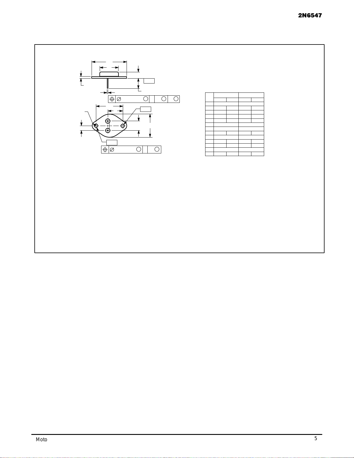
PACKAGE DIMENSIONS
NOTES:
1. DIMENSIONING AND TOLERANCING PER ANSI
Y14.5M, 1982.
2. CONTROLLING DIMENSION: INCH.
3. ALL RULES AND NOTES ASSOCIATED WITH
REFERENCED TO–204AA OUTLINE SHALL APPLY.
STYLE 1:
PIN 1. BASE
2. EMITTER
CASE: COLLECTOR
DIM MIN MAX MIN MAX
MILLIMETERSINCHES
A 1.550 REF 39.37 REF
B ––– 1.050 ––– 26.67
C 0.250 0.335 6.35 8.51
D 0.038 0.043 0.97 1.09
E 0.055 0.070 1.40 1.77
G 0.430 BSC 10.92 BSC
H 0.215 BSC 5.46 BSC
K 0.440 0.480 11.18 12.19
L 0.665 BSC 16.89 BSC
N ––– 0.830 ––– 21.08
Q 0.151 0.165 3.84 4.19
U 1.187 BSC 30.15 BSC
V 0.131 0.188 3.33 4.77
A
N
E
C
K
–T–
SEATING
PLANE
2 PLD
M
Q
M
0.13 (0.005) Y
M
T
M
Y
M
0.13 (0.005) T
–Q–
–Y–
2
1
U
L
G
B
V
H
CASE 1–07
TO–204AA (TO–3)
ISSUE Z
Page 6
2N6547
6
Motorola Bipolar Power Transistor Device Data
How to reach us:
USA / EUROPE: Motorola Literature Distribution; JAPAN: Nippon Motorola Ltd.; Tatsumi–SPD–JLDC, Toshikatsu Otsuki,
P.O. Box 20912; Phoenix, Arizona 85036. 1–800–441–2447 6F Seibu–Butsuryu–Center, 3–14–2 Tatsumi Koto–Ku, Tokyo 135, Japan. 03–3521–8315
MFAX: RMFAX0@email.sps.mot.com – TOUCHTONE (602) 244–6609 HONG KONG: Motorola Semiconductors H.K. Ltd.; 8B Tai Ping Industrial Park,
INTERNET: http://Design–NET.com 51 Ting Kok Road, Tai Po, N.T., Hong Kong. 852–26629298
Motorola reserves the right to make changes without further notice to any products herein. Motorola makes no warranty , representation or guarantee regarding
the suitability of its products for any particular purpose, nor does Motorola assume any liability arising out of the application or use of any product or circuit,
and specifically disclaims any and all liability, including without limitation consequential or incidental damages. “T ypical” parameters can and do vary in different
applications. All operating parameters, including “T ypicals” must be validated for each customer application by customer’s technical experts. Motorola does
not convey any license under its patent rights nor the rights of others. Motorola products are not designed, intended, or authorized for use as components in
systems intended for surgical implant into the body, or other applications intended to support or sustain life, or for any other application in which the failure of
the Motorola product could create a situation where personal injury or death may occur. Should Buyer purchase or use Motorola products for any such
unintended or unauthorized application, Buyer shall indemnify and hold Motorola and its officers, employees, subsidiaries, affiliates, and distributors harmless
against all claims, costs, damages, and expenses, and reasonable attorney fees arising out of, directly or indirectly, any claim of personal injury or death
associated with such unintended or unauthorized use, even if such claim alleges that Motorola was negligent regarding the design or manufacture of the part.
Motorola and are registered trademarks of Motorola, Inc. Motorola, Inc. is an Equal Opportunity/Affirmative Action Employer.
2N6547/D
*2N6547/D*
◊
 Loading...