

Page 1
Data Sheet
August 2001
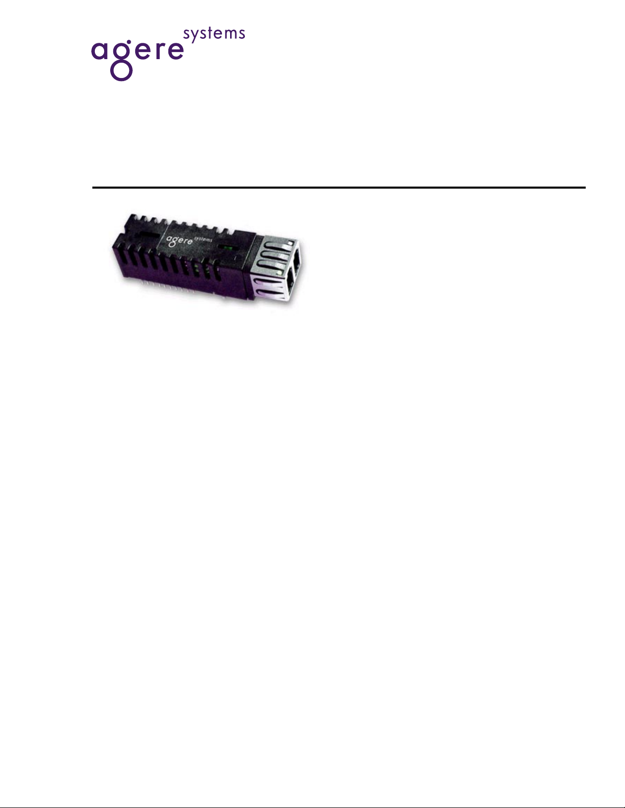
NetLight
®
1417K5A 2.5 Gbits/s
1300 nm Laser Transceiver with Clock and Data Recovery
Applications
■
SONET SR OC-48, SDH I-16 applications
■
High-speed, optical data inte rface for shelf-to-shel f
interconnect
Description
Available in a small form factor, RJ-45 size, plastic package,
the 1417K5A Transceiver is a high- performance, cost-effective, optical transceiver for SONET/SDH application s.
Features
■
Small form factor, RJ-45 size, 20-pin package
■
LC duplex receptacle
■
Uncooled 1300 nm laser transmitter with automatic
output power control
■
Transmitter disable input
■
Wide dynamic range receiver with InGaAs PIN
photodetector
■
Recovered clock outputs
■
TTL signal-detect output
The 1417K5A transceiv er i s a hi gh- speed, cost-effective optical transceiver intended for 2.488 Gbits/s
shelf-to-shelf optical interconnect appli cations as well
as SONET SR OC-48 and SDH I-16. The transceiver
features proven Agere Systems optics and is packaged in a narrow-width plastic housing with an LC
duplex receptacle. The receptacle fits into an RJ-45
form factor outline. The 20-pin package pinout conforms to a multisource transceiver agreement.
The transmitter f eatures the abil ity to interf ace to both
LVPECL and CML differential logic level data inputs.
The transmitter also f eatures a TTL logic le v el disab le
input and laser bias and back-facet monitor outputs.
The receiver f eatu res diff erential CML logic le v el data
and clock outputs, a TTL logic level signal-detect output and direct access to the PIN photodetector bias
input for photocurrent monitoring purposes.
■
Low power dissipation
■
Single 3.3 V power supply
■
LVPECL/CML compatible data inputs and CML
compatible data outputs
■
Operating temperature range: 0 °C to
70 °C
■
Agere Systems Inc. Reliability and Qualification
Program for built-in quality and reliability
Page 2
NetLight
1417K5A 2.5 Gbits/s Data Sheet
1300 nm Laser Transceiver with Clock and Data Recovery August 2001
Absolute Maximum Rat ings
Stresses in excess of the absolute maximum ratings can cause permanent damage to the device. These are absolute stress ratings only. Functional operation of the device is not implied at these or any other conditions in excess
of those given in the operations sections of the data sheet. Exposure to absolute maximum ratings for extended
periods can adversely affect device reliability.
Parameter Symbol Min Max Unit
Supply Voltage V
Operating Temperature Range T
Storage Temperature Range T
CC
stg
05V
C
070°C
–40 85 °C
Lead Soldering Temperature/Time — — 250/10 °C/s
Operating Wavelength Range λ 1.1 1.6 µm
Qualification and Reliabilit y
To help ensure high product reliability and customer satisfaction, Agere Systems is committed to an intensive quality program that starts in the design phase and proceeds through the manufacturing process. Optoelectronic modules are qualified to Agere Systems internal standards as well as other appropriate industry standards using MILSTD-883 test methods and procedures, and using sampling techniques consistent with
In addition, Agere Systems has been certified to be in full compliance with the latest
Telcordia
ISO
®
Standards.
®
requirements.
-9001 Quality System
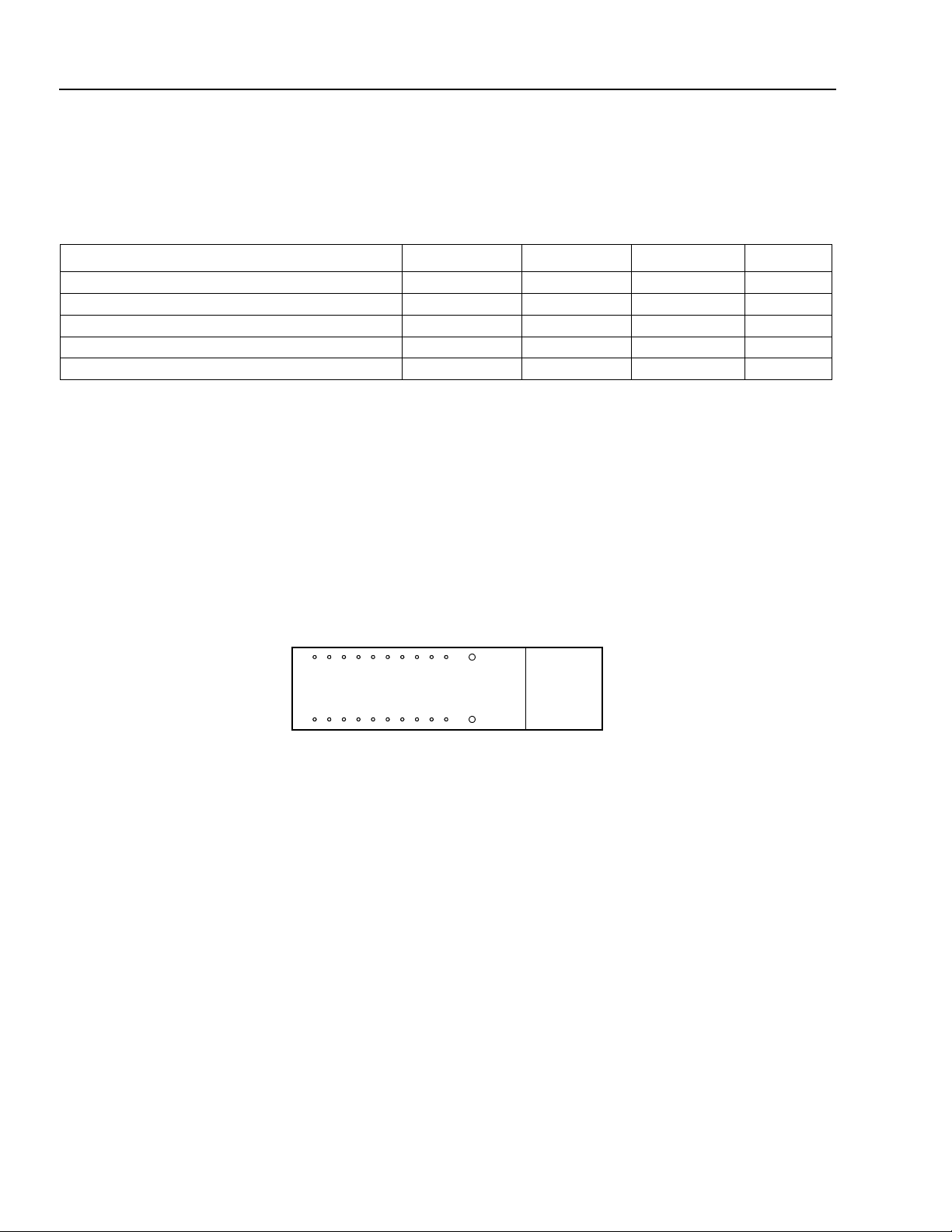
Pin Information
R
678910
1514131211
12345
2019181716
X
T
X
Figure 1. 1417K5A Transceiver, 20-Pin Configuration (top view)
1-967(F).d
2 Agere Systems Inc.
Page 3

Data Sheet
NetLight
1417K5A 2.5 Gbits/s
August 2001 1300 nm Laser Transceiver with Clock and Data Recovery
Pin Information
Table 1. Transceiver Pin Descriptions
Pin
Symbol Name/Description Logic Family
Number
MS MS
1V
2V
3V
PD
EER
EER
4CLK–
5CLK+
6V
7V
EER
CCR
8SD
9RD–
10 RD+
11 V
12 V
13 T
CCT
EET
DIS
14 TD+
15 TD–
16 NIC
17 B
18 B
19 P
20 P
MON
MON
MON
MON
Receiver
Mounting Studs.
The mounting studs are provided for transceiver
mechanical attachment to the circuit board. The y ma y also provi de an
optional connection of the transceiver to the equipment chassis
ground.
Photodetector Bias Input.
This lead supplies bia s for the PIN photo-
detector diode
Receiver Signal Ground.
Receiver Signal Ground.
Received Recovered
Clock
Out.
The rising edge occurs at the rising
edge of the Receiv e d Da ta outp ut. T he falling edge occurs in the middle of the Received Data baud period.
Received Recover Clock Out.
The falling edge occurs at the rising
edge of the Received Data output. The rising edge occurs in the middle of the Received Data baud period.
Receiver Signal Ground.
Receiver Power Supply.
Signal Detect.
Normal operation: logic 1 output.
Fault condition: logic 0 output
Received
DAT A
Out.
Received DATA Out.
Transmitter
Transmitter Power Supply.
Transmitter Signal Ground.
Transmitter Disable.
Transmitter DATA In
. An internal 50 Ω termination is provided, con-
sisting of a 100 Ω resistor between the TD+ and TD– pins.
Transmitter
DATA
In
. See TD+ pin for terminations. LVPECL/CML
No Internal Connection.
Laser Diode Bias Current Monitor, Negative End.
–
The laser bias
current is accessible as a dc voltage by measuring the voltage developed across pins 17 and 18.
Laser Diode Bias Current Monitor, Positive En d.
+
Optional feature;
if not used, do not connect. See pin 17 description.
Laser Diode Optical Power Monitor, Negative End.
–
Optional feature; if not used, do not connect. The back-facet diode monitor current is accessible as a voltage proportional to the photocurrent
through a 200 Ω resistor between pins 19 and 20.
Laser Diode Optical Power Monitor, Positive End.
+
Optional fea-
ture; if not used, do not connect. See pin 19 description.
NA
NA
NA
NA
CML
CML
NA
NA
LVTTL
CML
CML
NA
NA
LVTTL
LVPECL/CML
NA
NA
NA
NA
NA
Agere Systems Inc. 3
Page 4
NetLight
1417K5A 2.5 Gbits/s Data Sheet
1300 nm Laser Transceiver with Clock and Data Recovery August 2001
Electrostatic Discharge
Caution: This device is susceptible to damage as
a result of electrostatic discharge (ESD).
Take proper precautions during both
handling and testing. Follow
dard
EIA
-625.
EIA
®
Stan-
Although protection circuitry is designed into the
device, take proper precautions to avoid exposure to
ESD.
Agere Systems employs a human-body model (HBM)
for ESD susceptibility testing and protection-design
evaluation. ESD voltage thresholds are dependent on
the critical parameters used to define the model. A
standard HBM (resistance = 1.5 kΩ, capacitance =
100 pF) is widely used and, therefore, can be used for
comparison purposes. The HBM ESD threshold
established for the 1417K5A transceiver is ±1000 V.
Application Information
The 1417 receiver section is a highly sensitive fiberoptic receiver. Although the data outputs are digital
logic levels (CML), the device should be thought of as
an analog component. When laying out system application boards, the 1417 transceiver should receive the
same type of consideration typicall y given t o a sensitiv e
analog component.
Printed-Wiring Board Layout Considerations
A fiber-optic receiver employs a very high gain, widebandwidth transimpedance amplifier. This amplifier
detects and amplifies signals that are only tens of nA in
amplitude when the receiver is operating near its sensitivity limit. Any unwanted signal currents that couple
into the receiver circuitry cause a decrease in the
receiver's sensitivity and can also degrade the performance of the receiver's signal detect (SD) circuit. To
minimize the coupling of unwanted noise into the
receiver, careful attention must be given to the printedwiring board.
At a minimum, a double-sided printed-wiring board
(PWB) with a large component-side ground plane
beneath the transceiver must be used. In applications
that include many other high-speed devices, a multilayer PWB is highly recommended. This permits the
placement of power and ground on separate layers,
which allows them to be isolated from the signal lines.
Multilayer construction also permits the routing of sensitive signal traces away from high-level, high-speed
signal lines. To minimize the possibility of coupling
noise into the receiver section, high-level, high-speed
signals such as transmitter inputs and clock lines
should be routed as far away as possible from the
receiver pins.
Noise that couples into the receiver through the power
supply pins can also degrade performance. It is
recommended that a pi filter, shown in Figure 4, be
used for both the transmitter and receiver power
supplies.
Data, Clock, and Signal Detect Outputs
Due to the high switching speeds of CML outputs,
transmission line design must be used to interconnect
components. To ensure optimum signal fidelity, both
data outputs should be terminated identically. The signal lines connecting the data outputs to the ne xt device
should be equal in length and have matched impedances. Controlled impedance stripline or microstrip
construction must be used to preserve the quality of
the signal into the next component and to minimize
reflections back into the receiver, which could degrade
its performance. Excessive ringing due to reflections
caused by improperly terminated signal lines makes it
difficult for the component receiving these signals to
decipher the proper logic levels and can cause transitions to occur where none was intended. Also, by minimizing high-frequency ringing, possible EMI problems
can be avoided.
The signal-detect output is positiv e LVTTL logic. A logic
low at this output indicates that the optical signal into
the receiver has been interrupted or that the light level
has fallen below the minimum signal-detect threshold.
This output should not be used as an error rate indicator, since its switching threshold is determined only by
the magnitude of the incoming optical signal.
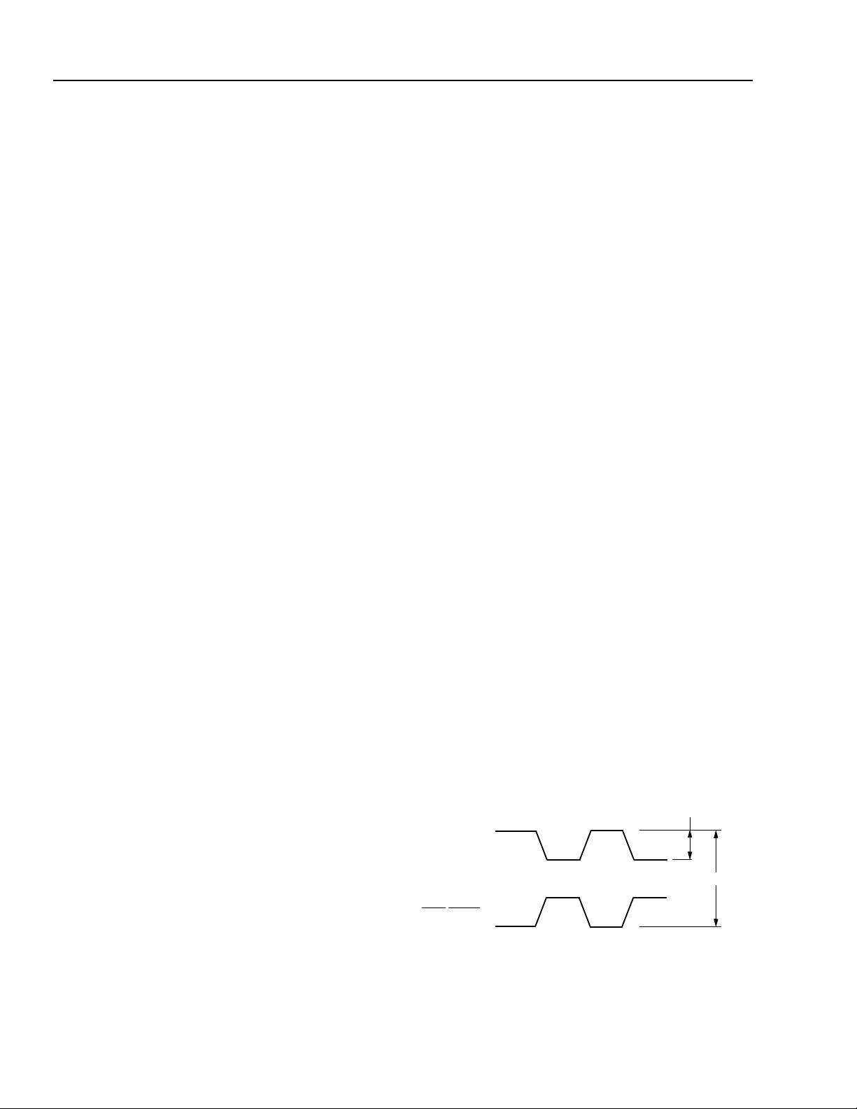
SINGLE ENDED
V
OH
DATA/CLOCK
V
OL
DIFFERENTIAL
V
OH
DATA/CLOCK
V
OL
1-1089F.a
Figure 2. Data Input/Output Logic Level Definitions
4 Agere Systems Inc.
Page 5
Data Sheet
NetLight
1417K5A 2.5 Gbits/s
August 2001 1300 nm Laser Transceiver with Clock and Data Recovery
Application Information
(continued)
Transceiver Processing
When the process plug is placed in the transceiver's optical port, the transceiver and plug can withstand normal
wave soldering and aqueous spray cleaning processes. However, the transceiver is not hermetic, and should not
be subjected to immersion in cleaning solvents. The transceiver case should not be exposed to temperatures in
excess of 125 °C. The transceiver pins can be wave soldered at 250 °C for up to 10 seconds. The process plug
should only be used once. After removing the process plug from the transceiver, it must not be used again as a
process plug; however, if it has not been contaminated, it can be reused as a dust cover.
Transceiver Optical and Electrical Characteristics
Table 2. Transmitter Optical and Electrical Characteristics
Parameter Symbol M in Max Unit
Average Optical Output Power (EOL) P
Optical Wavelength λ
Spectral Width ∆λ
Dynamic Extinction Ratio EXT 8.2 — dB
Output Optical Eye Compliant with SONET GR-253-CORE and
Power Supply Current I
Input Data Voltage:
Single Ended*
Differential*
Transmit Disable Voltage
Transmit Enable Voltage
†
†
Laser Bias Voltage V
Laser Back-Facet Monitor Voltage V
* 50 Ω load, measured single ended. Differential operation is necessary for optimum performance. (See Figure 2 for visual representation.)
† TTL compatible interface.
(T
= 0 °C to 70 °C; VCC = 3.135 V—3.465 V)
A
O
C
RMS
–10.0 –3.0 dBm
1266 1360 nm
—4nm
ITU-T G.957 Eye Mask Requirements
V
V
CCT
INp-p
INp-p
V
V
BIAS
D
EN
BF
—150mA
150
300
VCC – 0.9 V
EE
V
800
1600
CC
VEE + 0.8 V
0.0 0.7 V
0.01 0.2 V
mVp-p
mVp-p
V
Agere Systems Inc. 5
Page 6

NetLight
1417K5A 2.5 Gbits/s Data Sheet
1300 nm Laser Transceiver with Clock and Data Recovery August 2001
Transceiver Optical and Electrical Characteristics
Table 3. Receiver Optical and Electrical Characteristics
(T
= 0 °C to 70 °C; VCC = 3.135 V—3.465 V)
A
(continued)
Parameter Symbol Min Max Unit
MAX
CCR
I
— –18 dBm
–3 — dBm
— 350 mA
Average Sensitivity* P
Maximum Input Power* P
Power Supply Current I
Output Data/Clock Voltage:
Single Ended
Differential
†
†
OUTp-p
V
OUTp-p
V
300
600
500
1000
mVp-p
mVp-p
Clock Duty Cycle DC 45 55 %
Output Clock Random Jitter J
Output Clock Random Jitter Peaking J
‡
Clock/Data Alignment
Jitter Tolerance/Jitter Transfer
C
P
CDA
T
Telcordia
—0.01UI
—0.1UI
–40 40 ps
GR-253-CORE and ITU-G.958 Compliant
Signal-detect Switching Threshold:
Assert
Deassert
LST
LST
D
I
–45
—
–19
–18.5
dBm
dBm
Signal-detect Hysteresis HYS 0.5 6 dB
Signal-detect Voltage:
Low
High
Signal-detect Response Time SDRT — 100
*223 – 1 PRBS with a BER of 1 x 10
†50 Ω load, measured single ended. Dif ferential operation is necessary for optimum performance. (See Figure 2 for visual representation.)
‡ See Figure 3.
‡
OL
V
OH
V
0.0
2.4
0.8
V
CC
V
V
µ
–10
.
s
DATA
CLOCK
OUT
OUT
50%
50%
CDA
T
Figure 3. Clock Data/Alignment
1-725(F).b
6 Agere Systems Inc.
Page 7

Data Sheet
NetLight
1417K5A 2.5 Gbits/s
August 2001 1300 nm Laser Transceiver with Clock and Data Recovery
Transceiver Optical and Electrical Characteristics
MON–
B
MON+
B
MON–
P
MON+
V
15 k
15 k
PD
Ω
Ω
P
200
Ω
EET
V
NIC 16
TD–
TD+
DIS
T
CCT
V
CCR
V
RD+
RD–
CLK+
CLK–54
SD
12
15
14
13
11
7
1
10
9
8
17 18 19 20
Ω
15 k
Ω
10
Ω
15 k
TRANSMITTER
DRIVER
SFF TRANSCEIVER
PREAMP
RECEIVER
POST-
AMPLIFIER
(continued)
L2
C4 C5
C2 C3 C1
CC
V
L1
L1 = L2 = 1 µH—4.7 µH*
C1 = C2 = 10 nF
C3 = 4.7 µF—10 µF
C4 = C5 = 4.7 µF—10 µF
†
* Ferrite beads can be used as an option.
† For all capacitors, MLC caps are recommended
Figure 4. Power Supply Filtering of SFF Transceiver
EER
V
2, 3, 6
1-968(F).f
Agere Systems Inc. 7
Page 8

NetLight
1417K5A 2.5 Gbits/s Data Sheet
1300 nm Laser Transceiver with Clock and Data Recovery August 2001
Electrical Data Interface—Current Mode Logic (CML)
VCC (+3.3 V)
TD+
Ω
100
TD–
(A) TRANSMITTER INTERFACE—dc COUPLED—(CML)
VCC (+3.3 V)
RD+/CLK+
RD–/CLK–
Z = 50 Ω
Z = 50 Ω
Z = 50 Ω
Z = 50 Ω
V
CC
V
CC
CML
(+3.3 V)
(+3.3 V)
CML
(B) RECEIVER INTERFACE—dc COUPLED—(CML)
1-1033(F).e
Figure 5. 3.3 V Transceiver Interface with 3.3 V ICs and CML
8 Agere Systems Inc.
Page 9

Data Sheet
NetLight
1417K5A 2.5 Gbits/s
August 2001 1300 nm Laser Transceiver with Clock and Data Recovery
Alternate Electrical Data Interface Options
VCC (+3.3 V)
TD+
0.1 µF*
Ω
100
0.1 µF*
TD–
* Optional ac coupling capacitors; use ceramic X7R or equivalent.
(A) TRANSMITTER INTERFACE—ac OR dc COUPLED—(LVPECL)
VCC (+3.3 V)
RD+/CLK+
RD–/CLK–
0.1 µF
0.1 µF
Z = 50 Ω
Z = 50 Ω
Z = 50 Ω
Z = 50 Ω
130
130
CC
V
Ω
LVPECL
Ω
CC
(+3.3 V)
V
(+3.3 V)
CML
(B) RECEIVER INTERFACE—ac COUPLED—(CML)
1-1033F.d
Figure 6. 3.3 V Transceiver Interface with 3.3 V ICs
Agere Systems Inc. 9
Page 10

Data Sheet
NetLight
1417K5A 2.5 Gbits/s
August 2001 1300 nm Laser Transceiver with Clock and Data Recovery
Outline Diagrams
Package Outline
Dimensions are in inches and (millimeters).
1417
TRANSCEIVER
0.500
(12.70)
0.125
0.533
(13.54)
0.014 (0.36)
0.018
(0.46)
0.070
(1.78)(3.17)
1.479
(37.57)
1.922
(48.82)
0.350
(8.89)
0.400
(10.16)
0.443
(11.25)
0.040 (1.02)
0.299 (7.59)
0.387
(9.83)
0.105
(2.67)
0.530
(13.46)
0.246
(6.25)
1-968(F).d
Agere Systems Inc. 10
Page 11

Data Sheet
NetLight
1417K5A 2.5 Gbits/s
August 2001 1300 nm Laser Transceiver with Clock and Data Recovery
Outline Diagrams
Printed-Wiring Board Layout
(continued)
, †
*
Dimensions are in inches and (millimeters).
3.00
(0.118)
A
∅
(2x)
2.29 MAX
AREA FOR EYELETS
(0.090)
6.00
(0.236)
3.00
(0.118)
3.08
(0.121)
7.59
(0.299)
13.34
(0.525)
(2x)
(0.055 ± 0.004)
4.57
(0.180)
(0.280)
(9x) 1.78
(0.070)
∅
(2x)
(0.032 ± 0.004)
∅
∅
1.4 ± 0.1 NOTE 1
0.00 M A
∅
8.89
(0.350)
7.11
0.81 ± 0.1
0.00 M A
16.00 REF
(0.630)
2.00 (0.79)
(2x)
∅
2.29 MAX
(0.090)
2.01
(0.79)
9.59
(0.378)
10.16
(0.400)
NOTES:
1. HOLES FOR MOUNTING STUDS MUST BE TIED TO CHASSIS GROUND.
2. HOLES FOR HOUSING LEADS MUST BE TIED TO SIGNAL GROUND.
3.56
(0.140)
∅
(4x)
1.4 ± 0.1 NOTE 2
(0.055 ± 0.004)
0.00 M A
∅
1-1271(F)
* The hatched areas are keep-out areas reserved for housing standoffs. No metal traces of ground connection in keep-out area.
† Twenty-pin module shown; 10-pin module requires only 16 PWB holes.
Agere Systems Inc. 11
Page 12

NetLight
1417K5A 2.5 Gbits/s Data Sheet
1300 nm Laser Transceiver with Clock and Data Recovery August 2001
Outline Diagrams
(continued
Recommended Panel Opening
Dimensions are in inches and (millimeters).
0.560
(14.22)
0.400
(10.20)
0.100
(2.54)
0.039 TO 0.098
(1.00) TO (2.49)
0.590 TO 0.620
(14.98) TO (15.24)
1-1088(F)c
12 Agere Systems Inc.
Page 13

Data Sheet
NetLight
1417K5A 2.5 Gbits/s
August 2001 1300 nm Laser Transceiver with Clock and Data Recovery
Laser Safety Information
Class I Laser Product
FDA/CDRH Class I laser products. All versions of the transceiver are Class I laser products per CDRH, 21 CFR
1040 Laser Safety requirements. All versions are Class I laser products per
has been certified with the FDA under accession number 9520668.
CAUTION: Use of controls, adjustments, and procedures other than those specified herein may result in
hazardous laser radiation exposure.
This product complies with 21 CFR 1040.10 and 1040.11.
Wavelength = 1.3 µm
Maximum power = 1.58 mW
Product is not shipped with power supply.
NOTICE
Unterminated optical connectors may emit laser radiation.
Do not view with optical instruments.
®
IEC
60825-1:1993. The transceiver
Agere Systems Inc. 13
Page 14

NetLight
1417K5A 2.5 Gbits/s Data Sheet
1300 nm Laser Transceiver with Clock and Data Recovery August 2001
Ordering Information
Table 4. Ordering Information
Description Device Code Comcode
2 X 10 Single-Mode SFF LC Receptacle Transceiver
with Clock Recovery for 2.488 Gbits/s Applications
1417K5A 108748286
Telcordia
ISO
IEC
EIA
For additional information, cont act you r Agere Sys t em s Acc ount Manager or the following:
INTERNET:
E-MAIL:
N. AMERICA: Agere Systems Inc., 555 Union Boulevard, Room 30L-15P-BA, Allentown, PA 18109-3286
ASIA: Agere Systems Hong Kong Ltd., Suites 3201 & 3210-12, 32/F, Tower 2, The Gateway, Harbour City, Kowloon
EUROPE:
Agere Systems Inc. reserves the right to make changes to the product(s) or information contained herein without notice. No liability is assumed as a result of their use or application.
is a registered t rademark of Agere Systems I nc.
Copyright © 2001 Agere Systems Inc.
All Rights Reserved
August 2001
DS01-248OPT O
is a trademark of Telcordia Technologies Inc.
is a registered tra demark of The International Organization for Standardization.
is a registered trademark of the International Electrotechnical Commission.
is a registered trademark of Electronic Industries Association.
http://www.agere .com
docmaster@agere.co m
1-800-372-2447
Tel. (852) 3129-2000
CHINA:
JAPAN:
Tel. (44) 7000 624624
, FAX 610-712-41 06 (In CANA DA:
(86) 21-5047-1212
(81) 3-5421-1600
, FAX (852) 3129-202 0
(Shanghai),
(Tokyo ), KOREA:
, FAX (44) 1344 488 045
(86) 10-6522-5566
1-800-553-2448
(82) 2-767-1850
, FAX 610-712-4106)
(Beijing),
(86) 755-695-7224
(Seoul), SINGAPORE:
(Shenzhen)
(65) 778-8833
, TAIWAN:
(886) 2-2725-5858
(Taipei)
NetLight
 Loading...