

Page 1

Service Manual
Model :
DV -K1 1WZ-PB/A
DV -K1 1WY-PB
DV -K1 1WZ-QB/A
DAEWOO ELECTRONICS CO., LTD
OVERSEAS SERVICE DEPT.
Page 2

GENERAL
Power requirement AC90~260V, 50/60Hz
Power consumption Typical 13W
Temperature 5¡£C~35¡£C (Operating)
-20
C~60 C
(Storage temperature)
Operating position Horizontal only
Dimensions (WxHxD) 360x90x312 (mm)
Weight Approx 5.4kg
Format VHS standard
Tape widch 12.65mm
Tape speed (SP): 23.39mm/sec
Maximum recording time
with full-size cassette (SP): 240 min. with E-240
video cassette
Maximum recording time
with full-size cassette (SP): 45 min. with E-45
cassette
VIDEO
Signal system PAL color and CCIR
monochrome signals,
625 lines/50 fields
Recording system Rotary two-head helical scan
with a slant double-azimuth
combination video head
Input 1.0Vp-p, 75 ohms, unbalanced
Output 1.0Vp-p, 75 ohms, unbalanced
Simal to noise rallio
More than 43 dB (Rohde & Schwarz
noise mater)
Horizontal resolution
More than
240 lines
AUDIO
Input -8 dBs, (CENELEC standard)
more than 47 k-ohms, unbalanced
Output -6 dBs, (CENELEC standard),
less than 1 k-ohm, unbalanced
(10 k-ohms, load)
Frequency range 100 Hz to 8,000 Hz
/20 Hz to 20 KHz (Hi-Fi)
Signal to noise ratio 38 dB (More than)
/60dB (More than):Hi-Fi
Audio Distortion Less than 3%(SP)
/Less than 0.5%(SP):Hi-Fi
RF Output UHF channel 36
(Adjustable 30~39)
ACCESSORIES
Provided Accessories Remote control unit
RF Cable, Battery
• Design and specifications can be subjected to change
without notice.
Page 3
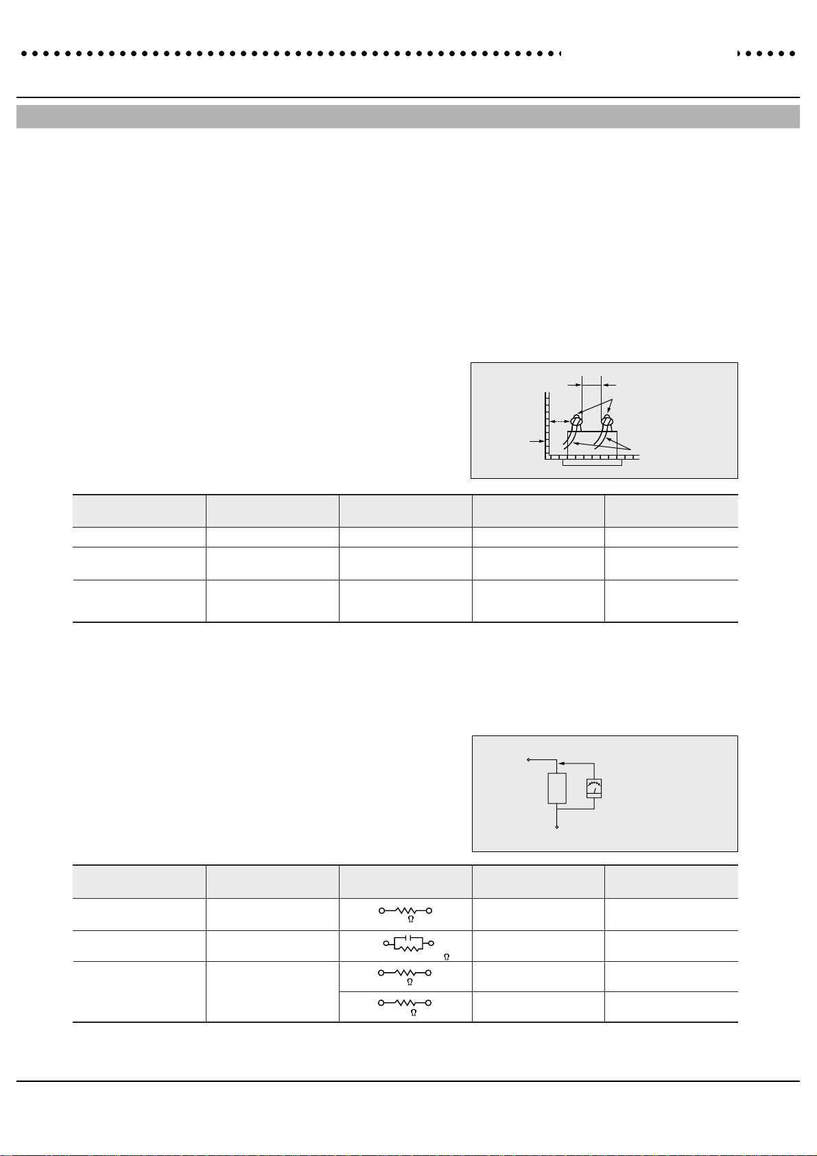
SAFETY CHECK AFTER SERVICING
Examine the area surrounding the repaired location for damage or deterioration. Observe that screws, parts and wires
have been returned to original positions. Afterwards, perform the following tests and confirm the specified values in order
to verify compliance with safety standards.
1. Insulation resistance test
Confirm the specified insulation resistance or greater between power cord plug prongs and externally exposed parts of
the set (RF terminals, antenna terminals, video and audio input and output terminals, microphone jacks, earphone
jacks, etc.). See table below.
2. Dielectric strength test
Confirm specified dielectric strength or greater between power cord plug prongs and exposed accessible parts of the
set (RF terminals, antenna terminals, video and audio input and output terminals, microphone jacks, earphone jacks,
etc.) See table below.
3. Clearance distance
When replacing primary circuit components, confirm specified
clearance distance (d), (d') between soldered terminals, and
between terminals and surrounding metalic parts. See table below.
Table 1: Rating for selected areas
* Class II model only.
Note: This table is unofficial and for reference only. Be sure to confirm the precise values for your particular country and
locality.
4. Leakage current test
Confirm specified or lower leakage current between B (earth ground, power cord plug prongs) and externally exposed
accessible parts (RF terminals, antenna terminals, video and audio
input and output terminals, microphone jacks, earphone jacks, etc.)
Measuring Method: (Power ON)
Insert load Z between B (earth ground, power cord plug prongs)
and exposed accesible parts. Use and AC voltmeter to measure
across both terminals of load Z. See figure 2 and following table.
Table 2: Leakage current ratings for selected areas
Note: This table is unofficial and for reference only. Be sure to confirm the precise values for your particular country and
AC Line Voltage Region
Insulation Dielectric Clearance
Resistance Strength Distance (d), (d')
100V Japan ≥ 1 MΩ/500 V DC 1kV AC 1 minute ≥ 3 mm
110 to 130V
USA &
– – –
900V AC 1 minute ≥ 3.2mm
Canada
* 110 to 130 V Europe ≥4 MΩ/500 V DC 3 kV AC 1 minute ≥ 6 mm (d)
200 to 240 V Australia ≥ 8 mm (d')
AC Line Voltage Region
Earth Ground
Load Z Leakage Current (i)
(B) to:
100V Japan ¡ ≤ 1m A rms
Exposed accessible
parts
110 to 130 V USA & ¡ ≤ 0.5 m A rms Exposed accessible
parts
¡ ≤ 0.7 m A peak Antenna earth
110 to 130 V Europe ¡ ≤ 2 m A dc terminals
200 to 240 V Australia ¡ ≤ 0.7 m A peak
Other terminals
1k
1.5k
1.5kµF
2k
50k
Fig. 1
Fig. 2
INFORMATION
Chassis
d
Primary circuit termimals
d'
a
Exposed
accessible
part
Z
AC Voltmter
(high impedance)
Earth Ground
power cord plug prongsB
Page 4

1. CONTROLS AND FUNCTIONS
...................................................................................................2
2. ELECTRICAL ADJUSTMENTS
2-1. SERVO CIRCUIT ADJUSTMENT METHOD.......................................................................................3
2-2. AUDIO CIRCUIT ADJUSTMENT METHOD........................................................................................4
3. TROUBLE SHOOTING FLOW CHART
3-1. POWER CIRCUIT.................................................................................................................................5
3-2. SERVO-SYSCON CIRCUIT.................................................................................................................7
3-3. AUDIO CIRCUIT (NORMAL)..............................................................................................................12
3-4. AUDIO CIRCUIT (HI-FI)......................................................................................................................14
3-5. VIDIO CIRCUIT ..................................................................................................................................16
4. WA VEFORMS ON VIDEO CIRCUIT
........................................................................................22
5. µ-COM PART
.......................................................................................................................................25
6. CIRCUIT DIAGRAM
..........................................................................................................................27
6-1. CONNECTION DIAGRAM .................................................................................................................27
6-2. POWER CIRCUIT DIAGRAM.............................................................................................................28
6-3. SERVO/SYSCON CIRCUIT DIAGRAM.............................................................................................29
6-4. VIDEO & HEAD-AMP CIRCUIT DIAGRAM.......................................................................................30
6-5. AUDIO CIRCUIT DIAGRAM............................................................................................................... 31
6-6. HI-FI AUDIO CIRCUIT DIAGRAM......................................................................................................32
6-7. KARAOKE CIRCUIT DIAGRAM.........................................................................................................33
6-8. LOGIC SW CIRCUIT..........................................................................................................................34
7. COMPONENTS LOCA TION GUIDE ON PCB BOTTOM VIEW
.................................35
8. DISASSEMBLY
8-1. PACKING ASSEMBLY.......................................................................................................................37
8-2. SET ASSEMBLY.................................................................................................................................38
8-3. PAN ASSEMBLY................................................................................................................................ 39
9. ELECTRICAL PARTS LIST
............................................................................................................40
Z-PB/A DV-K11WY-PB DV-K11WZ-QB/A DV-K11WZ-PB/A DV-K11WY-PB DV-K11WZ-QB/A DV-K11WZ-PB/A DV-K11WY-PB D
V-K11WZ-PB/A DV-K11WY-PB DV-K11WZ-QB/A DV-K11WZ-PB/A DV-K11WY-PB DV-K11WZ-QB/A DV-K11WZ-PB/A DV-K11W
Z-PB/A DV-K11WY-PB DV-K11WZ-QB/A DV-K11WZ-PB/A DV-K11WY-PB DV-K11WZ-QB/A DV-K11WZ-PB/A DV-K11WY-PB D
V-K11WZ-PB/A DV-K11WY-PB DV-K11WZ-QB/A DV-K11WZ-PB/A DV-K11WY-PB DV-K11WZ-QB/A DV-K11WZ-PB/A DV-K11W
Z-PB/A DV-K11WY-PB DV-K11WZ-QB/A DV-K11WZ-PB/A DV-K11WY-PB DV-K11WZ-QB/A DV-K11WZ-PB/A DV-K11WY-PB D
V-K11WZ-PB/A DV-K11WY-PB DV-K11WZ-QB/A DV-K11WZ-PB/A DV-K11WY-PB DV-K11WZ-QB/A DV-K11WZ-PB/A DV-K11W
Z-PB/A DV-K11WY-PB DV-K11WZ-QB/A DV-K11WZ-PB/A DV-K11WY-PB DV-K11WZ-QB/A DV-K11WZ-PB/A DV-K11WY-PB D
V-K11WZ-PB/A DV-K11WY-PB DV-K11WZ-QB/A DV-K11WZ-PB/A DV-K11WY-PB DV-K11WZ-QB/A DV-K11WZ-PB/A DV-K11W
VIDEO CASSETTE RECORDER
Page 5
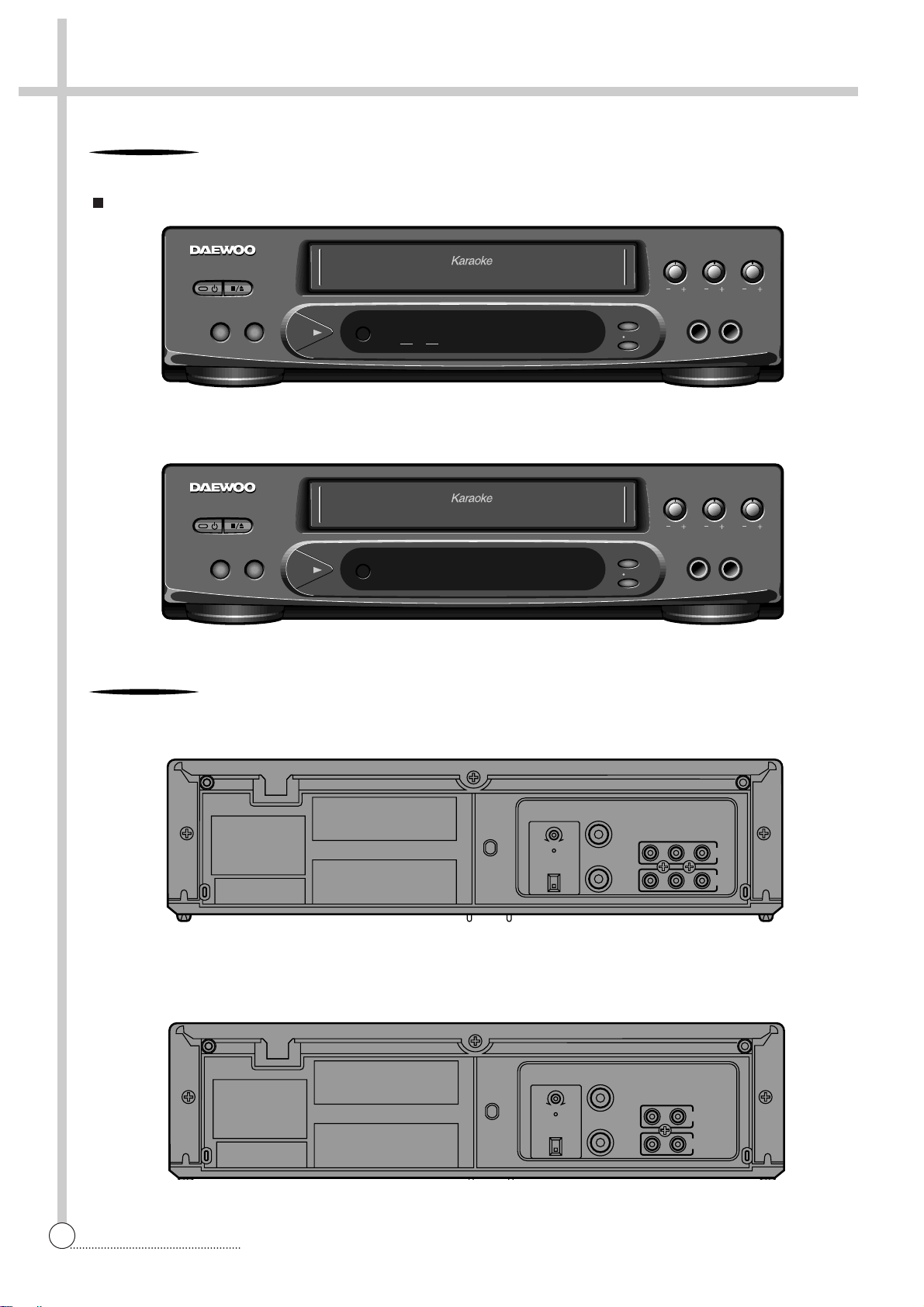
1. CONTROL AND FUNCTIONS
FRONT
DV-K11WZ-PB/A
DV-K11WY-PB (Hi-Fi)
DV-K11WZ-QB/A (NORMAL)
REAR
2
PLAY
AUTO REPEAT
REC
DIGITAL ECHO
VOL 1 VOL 2
MIC 1 MIC 2
PAUSE/STILL
REW PLAY FF
L Hi-Fi R
CST.IN NTSC A.REPEAT REC
DV-K11W
POWER STOP/EJECT
NTSC PLAY BACK RECORDING • HIGH SPEED REWIND
#
PLAY
AUTO REPEAT
REC
DIGITAL ECHO
VOL 1 VOL 2
MIC 1 MIC 2
PAUSE/STILL
REW PLAY FF CST.IN NTSC A.REPEAT REC
DV-K11W
POWER STOP/EJECT
NTSC PLAY BACK RECORDING • HIGH SPEED REWIND
#
RF OUT
CH.R CH.L
TEST
ON
OFF
ANT. IN
VIDEO AUDIO
LR
IN
OUT
RF OUT
CH.R CH.L
TEST
ON
OFF
ANT. IN
VIDEO AUDIO
IN
OUT
Page 6
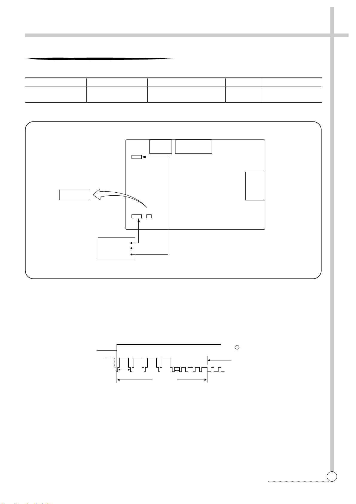
SERVO CIRCUIT ADJUSTMENT METHOD
VIDEO HEAD SWITCHING POSITION
! Connection Method
@ Adjustment Procedure
1. Play back the test tape.(STAIR STEP DP-2)
2. Set the oscilloscope in the chop mode. Connect CH1 to the SW pulse(PT01 PIN#), and CH2 to the VIDEO
OUT(R305 ) and trigger the scope with signal from CH1.
3. Adjust R595 to the positive rising edge of SW PULSE at 6.5H±0.5H from the V-SYNC.
2. ELECTRICAL ADJUSTMENT
3
Adjustment Parts Checking Point Measuring Equipment Mode Test Tape
R305 DP-2
R595
PT01 PIN ¤Ø
Oscilloscope PLAY
(STAIR STEP)
CH1
CH2
1H
0.5H
6.5H ± 0.5H
VERTICAL SYNC
SW 30Hz
(PT01 PIN)
(R305)
TRIGGER
3
R305
PHONE
JACK
MODULATOR
POWER
6.5H±0.5H
PT01 R595
MODULE
TOP VIEW
OSCILLOSCOPE
CH-1
CH-2
Page 7
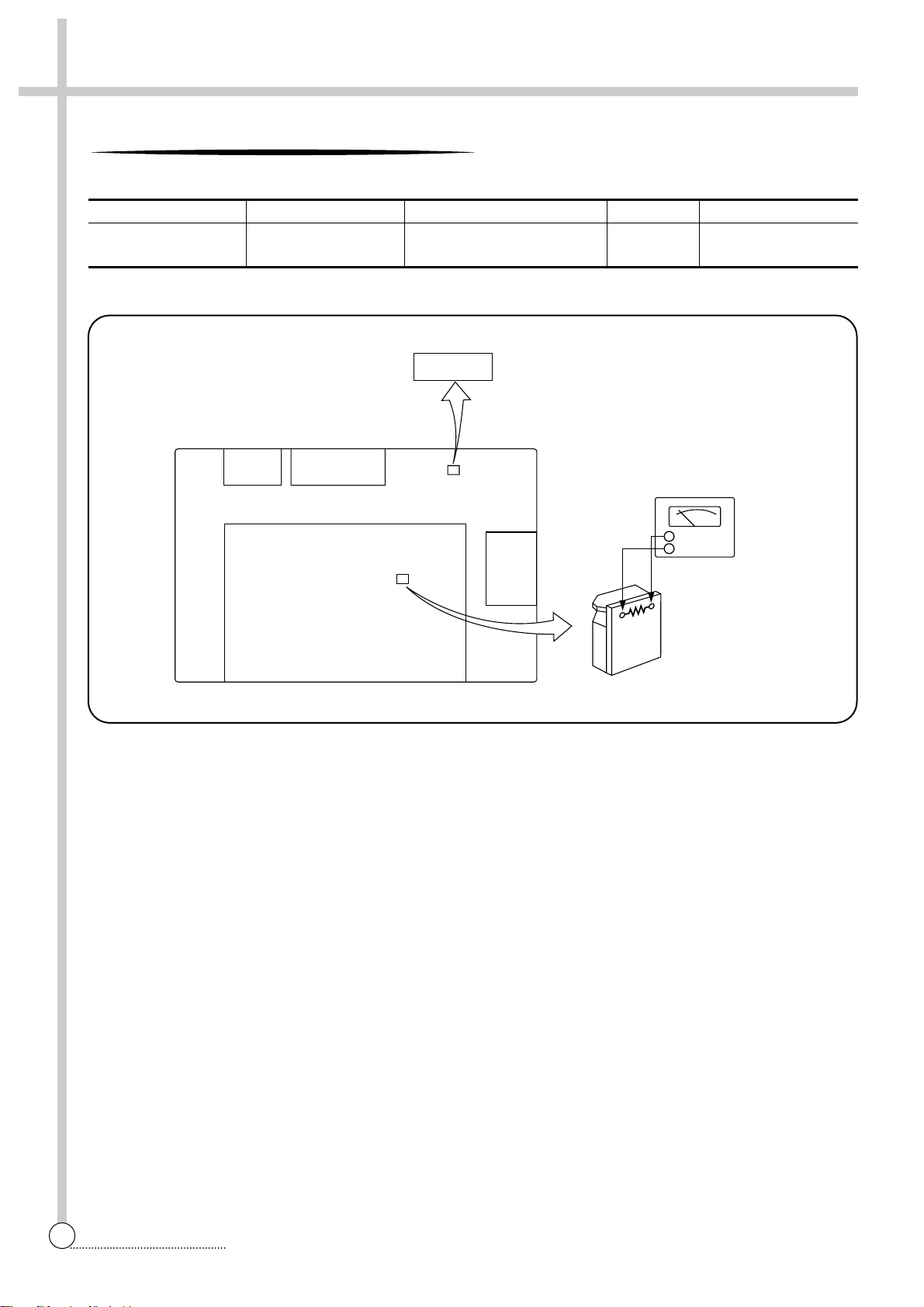
AUDIO CIRCUIT ADJUSTMENT METHOD
AUDIO RECORD BIAS
! Connection Method
@ Adjustment Procedure
1. Set the power on mode.
2. Set the input to open mode
3. Connect the Audio level meter to R01
4. After inserting a blank tape, record in SP mode.
5. Adjust R292 to obtain 3.0 mVrms.
4
Adjustment Parts Checking Point Measuring Equipment Test Tape Input Signal
R292
A/C Head PCB
Audio level meter Rec None signal
R01
3.0mVrms
PHONE
JACK
MODULATOR
DECK ASSY
A/C HEAD
R292
POWER
MODULE
A/CHEAD
Audio LEVEL METER
+
–
R01
Page 8
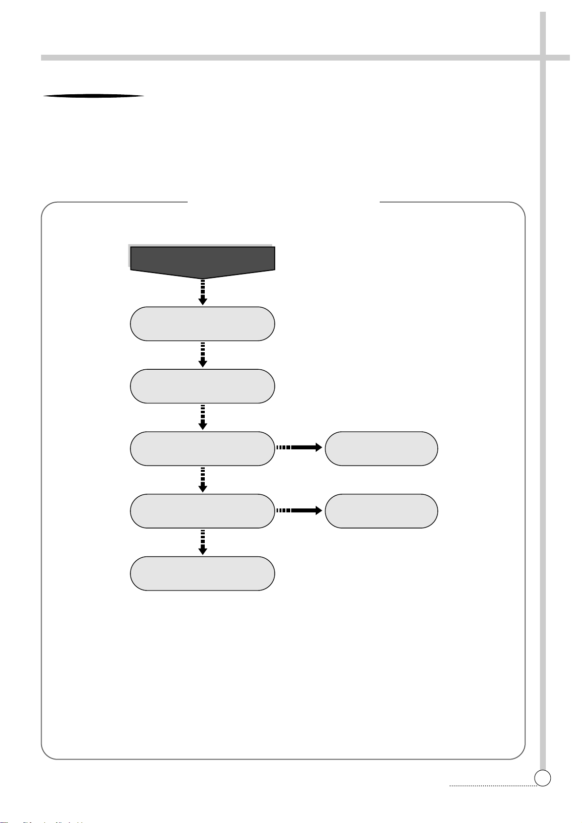
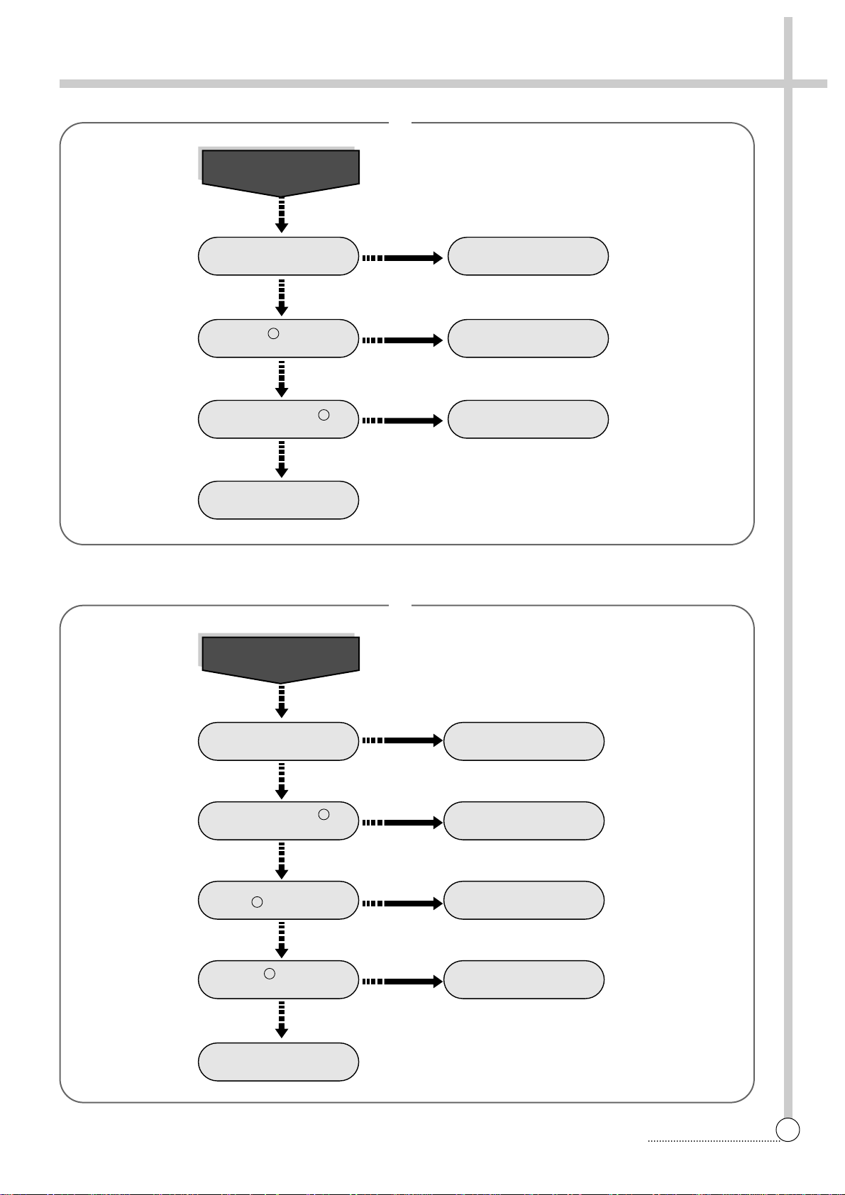
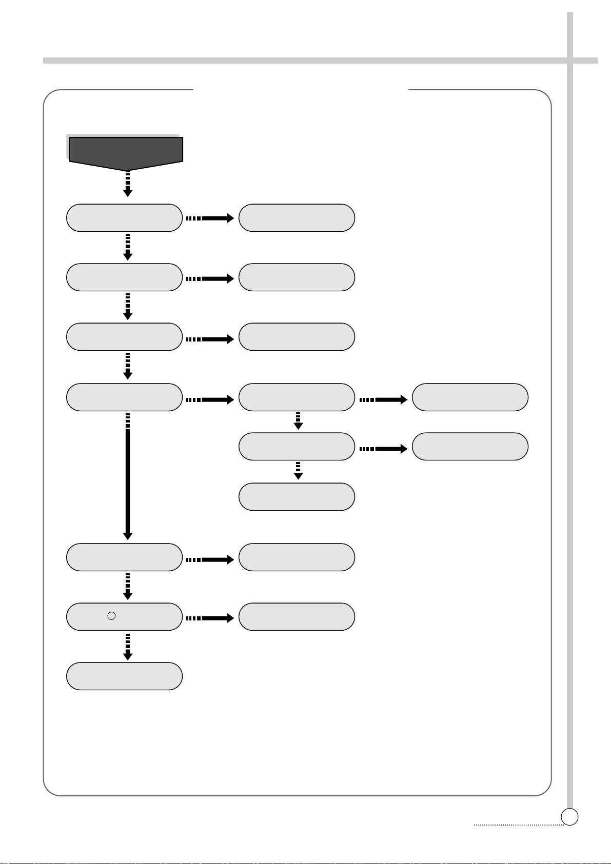
3. TROUBLE SHOOTING FLOW CHART
POWER CIRCUIT
• When change the parts which are out of order, first, remove the power plug from the socket and then discharge the
voltage across between both terminals of C807. (Use an external scores of KΩresistance)
• When check the primary circuit by using the oscilloscopes insulate the oscilloscope surely. (Use the isulating
transformer) and must connect GND into the primary GND), (But there is no connection when check the secondary
circuit).
• When change SM801(POWER MODULE), check FUSE and Cement resistance surely.
5
YES
NO
NO
YES
YES
YES
YES
Prepare the instrument
connecting the insulating trans.
Check F801 FUSE
Is voltage applied to D801?
Is voltage applied to the
both terminals of C807?
Check power module
Check D801, L801
Check R802
NO output Voltage
Page 9
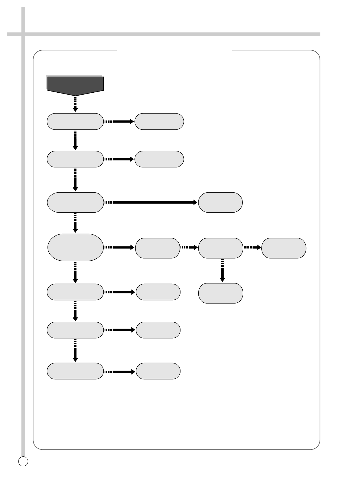
6
Is voltage supplied
Via CN11?
The voltage of #1 of
IC11 is 5.7V and stable
The voltage of #1 of IC11
fluctuate
in 4.8V~5.7V
Measure resistance
between GND of CN21
and each terminal
of CN21
The 12DC of each
wire of T11 is ok
Primary parts is ok
Secondary parts ok
Change T11
Change parts
out of order
YES
NO
YES
Resistance >> 100Ω
YES
YES
NO
Check F801, L801,
D802
NO
Check the secondary
circuit
YES
YES
Check the pattern
and T11, L11, IC11
NO
NO
Terminal open and
measure the output
Voltage
Change parts
out of order
The voltage
is ok
Check the
parts outside
module
Check the Diode,
Condenser inside
Module
NO
NO
No Voltage
output
Page 10
SERVO SYSCON CIRCUIT
7
58
The voltage of pin
of IC601 is not
changed.
Is CTL pulse input
to pin IC501
7
20
Check and
re-adjust the
Path of Deck.
Check circuit
adjacent to IC601
Check C503, C504,
C506
check R539, C518
Check IC601
YES
YES
YES
YES
YES
YES
YES
NO
NO NO
NO
NO
NO
Noise appears
although adjusting
tracking.
Is CTL pulse out
from pin of IC601.
Noise shakes up
and down on the
screen.
Adjust
tracking
CTL HEAD height is
normal and there is
not dust.
Adjust the HEAD
height and remove
dust
Noise appears
although change
cassette tape.
Playback picture
is not good.
A
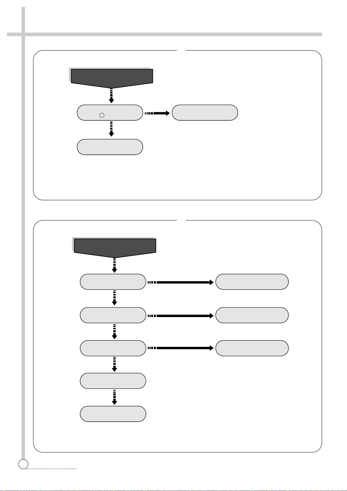
Page 11
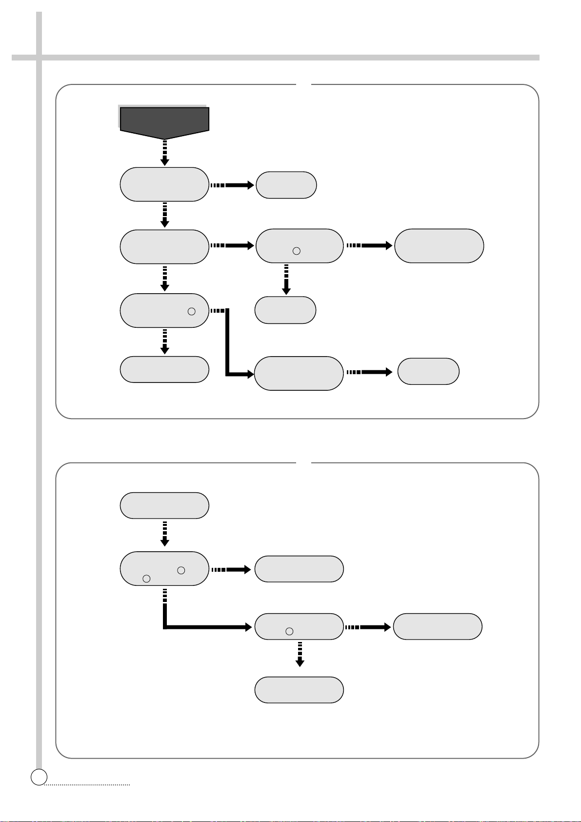
8
Playback picture
is not good.
Noise appears
on the screen
on the whole.
Is Enve.wavefrom
supplied to at pin of
PT01
4
Are SW pulse
applied to
HeadAmp circuit?
Check video circuit.
Check flow A
Is SW pulse supplied
from pin of IC601?
23
Check D.PG input
and connector.
Check pattern
Check connector, Head
Amp and Head dust.
Change head
YES
NO
NO
YES
YES
YES
YES
NO
NO
B
Auto stop during
playback
Is Reel pulse
applied to pin and
of IC601?
7
14
Check reel sensor.
Is D.FG applied to
pin of IC601
Check connector
D.FG circuits.
Check IC601
YES
YES
NO
YES
NO
17
C
Page 12
9
Is Motor 12V supplied?
Is pin D.FG of
IC601 supplied.
Is pin D.PWM (pin )
of IC601 supplied?
Check connector
and Motor.
17
30
Check
POWER MODULE
Check C509, R523
Check IC601
YES
YES
YES
NO
NO
NO
Drum M/T loading stops.
D
Is the input of pin
of PJ502 2V-3.5V?
Is pin of PJ502 2.5V
Is pin (C.PWM)
of IC601 Supplied?
Check connector
and Motor
4
Check power circuit.
Check circuit of R515,
R516, R517.
Check R541, R542
Check IC601
YES
YES
YES
YES
YES
NO
NO
NO
NO
Is Motor 12V supplied?
Capstan M/T loading stops.
31
6
E
Page 13
10
Is C. Sync applied to
pin of IC601?
Check Motor.
Check C. Sync of
IC 401 and Pattern
NO
YES
NO
Drum M/T and Capstan M/T rotate
at regular speed. (In REC mode)
8
F
Is EVER 5V supplied?
Does X601 crystal osciliate?
Is CAM SW DATA Correct?
Check IC502.
Check IC 601.
Check power circuit.
Check IC601 and X601.
Recheck connector
and CAM SW contact.
YES
YES
YES
YES
NO
NO
NO
Emergency mode when plugging
(Power cord)
G
Page 14
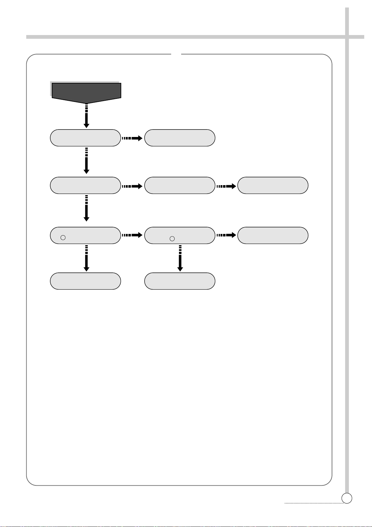
11
Cassette is not
inserted.
Is Motor 12V supplied?
Check power
circuit
CAM DATA is changed
when CST IN?
Is 5V applied to
pin of IC502 when CST IN?
Chek IC502
Check connector. Check DECK part.
Is 5V supplied at
pin of IC601?
Check PATTERN
Check IC601
NO
YES
YES
YES
NO NO
NO NO
YES
4
37
H
Page 15
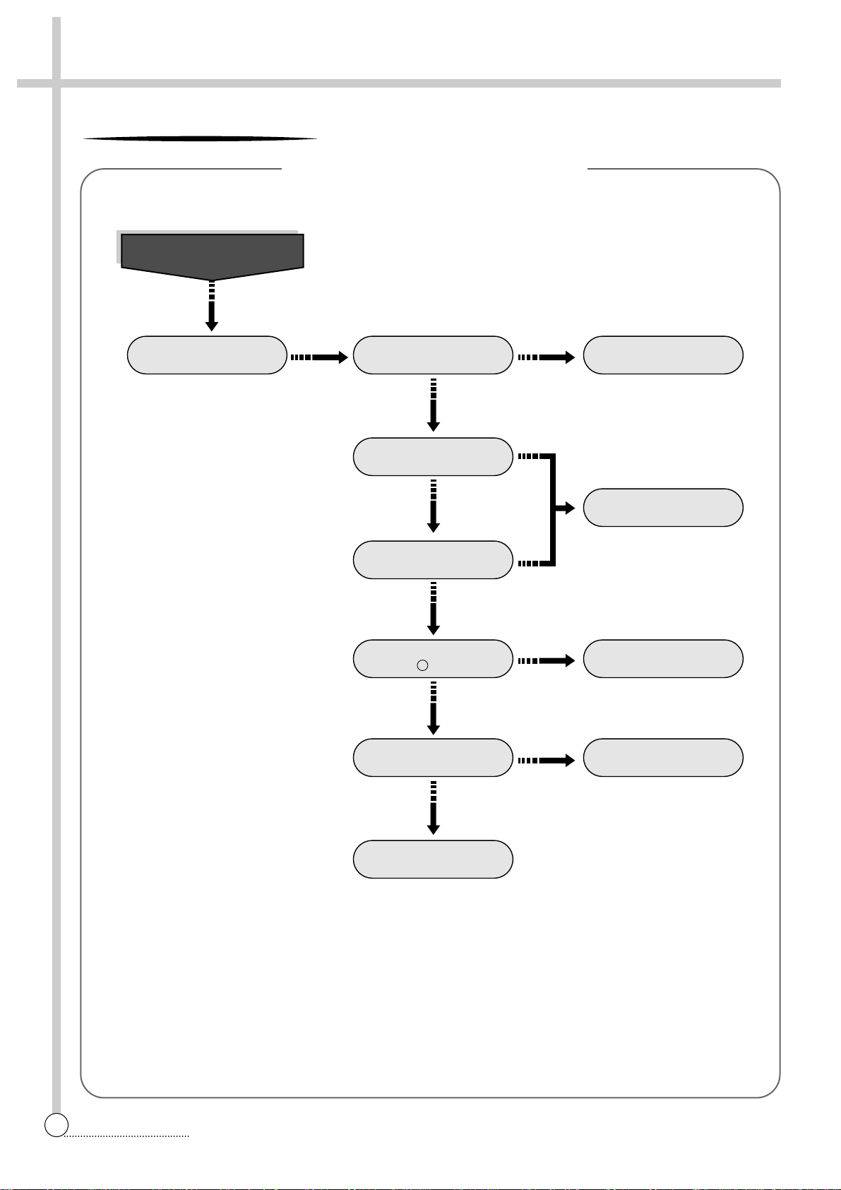
12
AUDIO CIRCUIT (NORMAL)
No sound in the playback mode.
Is the output at pin‘
of IC201?
Is 9V applied to pin &
of IC201?
Check power circuit.
Is 5V applied to
1of IC201?
Is there Audio output
at pin of IC201?
Check PJ504
and HEAD.
Check circuit adjacent
to R211, R212
NO NO
YES
YES
YES
YES
NO
NO
Is pin=of IC201 0V?
NO
Check IC 601
Is pin # of IC201
GND?
Check IC201
YES
NO
10
Page 16
13
Is the signal applied to
pin 6 of IC201?
Is 5V applied to
pin = of IC201?
Is there output at pin “
of IC201?
Does T201 oscillate?
Check IC601.
Check IC201.
Is the voltage above 10V
at pin # of T201?
Check T201
Is record current
3.0mVrms?
Is pin of IC201 0V?
Clean HEAD.
Asjust Record current.
Check IC201.
NO
YES
YES
YES
YES
YES
NO
NO
NO
NO
No sound in the playback
mode after recording
Check circuit adjacent
R209, R210, C207
Check Q201
collector:above 10V
Base: 0V
Check Q202 and T201.
NO
NO
Check Q201.
NO
1
Page 17

14
AUDIO CIRCUIT (HI-FI)
No sound in the E-E mode.
Is 12V applied to pin
a of IC901?
Is signal input into pin ^, &
of IC901 in LINE mode?
Check
PHONE jack
YES
YES
YES
NO
NO
Is 5V applied to pin 3
g of IC901?
NO
Check
POWER circuit
Is 5V and clock data applied
to pin 4, 5 of IC901?
Check IC601
YES
NO
Check
PHONE Jack
YES
Is there output at
pin “, ‘ of IC901?
Change IC901
NO
Page 18

15
Is the ENVE level of
C919 more than 120mVp-p?
Is A.SW PULSE input into
pin J of IC901?
Is 5V and clock data applied
to pin 4, 5 of IC901?
Is signal input into pin S, k
of IC901
Check pin = of IC601
Check IC601
Is there output at
s, K of IC901?
Is there output at
pin “, ‘ of IC901
Check PHONE jack
Change IC901.
NO
YES
YES
YES
YES
NO
NO
NO
No Hi-Fi Sound
in playback mode
Check the ICH01
of PRE-AMP circuit
Check CK13, CM13
NO
NO
YES
Page 19

16
VIDEO CIRCUIT
Is video signal input
into pin of IC301?
31
Is signal output from
pin of IC301?
Is 5V supplied to pin
and of IC301?
26
54
Check
power circuit
Is Serial clock and data
signal input into
pin , of IC301?
Check
IC601 , pin
1
Check RF out Check Line out
YES
YES
YES
NO
NO NO
14 15
NO
YES
Is QV SYNC(H) supplied to
anode of D301 at 5 volts?
YES
Check IC601
Check PHONE jack
27
2
Page 20

17
Is the video signal from pin of IC301?
NO
YES
Check PHONE jack
31
Is ON/OFF 5V supplied to pin and
pin of IC301 at 5volts?
NO
YES
Check 5V CIRCUIT
(IC801, Q802, Q803)
26
54
Is REC(H) supplied to anode of
DA01 at 4.2 volt?
NO
YES
Check IC601 Pin
Is the down-converted color signal
obtained from pin of IC301?
NO
YES
Change IC301
2
Is the down-converted color signal
from pin of IC301 fed to RA04?
YES
Check ICA01 and pattern
2
To HEAD AMP IC
NO
NO
YES
Check IC302
44
Is the down-converted color signal
from pin of IC301 fed to pin of IC301?
55 56
Page 21

18
NO
YES
Check PHONE jack
and pattern
Is ON/OFF 5V supplied to pin
and pin of IC301 at 5volts?
NO
YES
Check ON/OFF 5V CIRCUIT
(IC801, Q802, Q803)
Is REC(H) supplied to anode of
DA01 at 4.2volt?
NO
YES
Check IC601 Pin
Is the video signal from pin
of IC301 fed to pin of IC301?
NO
YES
Check IC301
Is the luminance signal from pin
of IC301 fed to pin of IC301?
YES
Check C302
31
26
31
38
35
36
Is the luminace signal from pin
of IC301 fed to pin of IC301?
NO
Is QV SYNC (H) supplied to
anode of D301 at 0 volt?
Check QV SYNCChange IC301
NO
47
52
YES
YES
Check record EQ circuit
To HEADAMP IC
NO
NO
Is the video signal obtained from
pin of IC301?
44
54
Is the modulating luminance signal
from pin of IC301 fed to pin of ICA01?
52 15
Page 22

19
Is PB-FM signal from HEA DAMP
fed to pin of ICA01?
NO
YES
Check HEAD AMP circuit
Is ON/OFF 5V supplied to pin and
pin of IC301 at 5volts?
NO
YES
Check ON/OFF 5V CIRCUIT.
26
Is REC(H) supplied to anode of
DA01 at 0volt?
NO
YES
Check IC601 Pin
Is Y-FM signal from pin of
ICA01 fed to pin of IC301?
NO
YES
Check PB EQ CIRCUIT
(QA01, QA02, QA03)
Is the luminance signal from pin
of IC301 fed to pin of IC301?
Check IC301
11
51
47
38
YES
Is the luminance signal from pin of IC301
fed to pin of IC301
Check IC302
38
35
YES
Is the luminance signal from of IC301
fed to pin of IC301?
Change IC301
35
27
YES
Check RF out
NO
NO
NO
11
Check Line out
44
54
Page 23

20
Is the PAL color signal from pin of
ICA01 fed to pin of IC301 through
AMP circuit?
NO
YES
Check HEAD AMP circuit
Is ON/OFF 5V supplied to pin and
pin of IC301 at 5volts?
NO
YES
Check ON/OFF 5V CIRCUIT
Is QV SYNC supplied to anode of
D301 at 0 volts?
NO
YES
Check QV SYNC
Is the PAL color signal from pin
of IC301 fed to pin of IC302?
Check IC301 pin , serial
clock and data input
YES
Is the signal from pin
of IC301 fed to pin
of IC301
Check IC302
YES
11
53
26
53
55
55
56
Is color signal output from
pin of IC301?
Change IC301
27
YES
Check RF out
NO
NO
NO
Check Line out
Is the signal from pin of
IC301 fed to pin of IC301
Check IC301
YES
56
23
NO
54
1514
Page 24

21
Is the miexd modulating luminance
signal and down converted color signal
obtained from pin of ICA301?
NO
YES
Check REC Y EQ and
RA04 and pattern
Is ON/OFF 5V supplied to pin of
ICA01 at 5volts?
NO
YES
Check ON/OFF 5V CIRCUIT
Is REC (H) supplied to pin
of ICA01 at 4.2volts?
NO
YES
Check IC601 Pin
Is the signal from pin of ICA01?
Check ICA01
YES
To HEAD
10
15
11
1
NO
44
Page 25

4. WA VEFORMS ON VIDEO CIRCUIT
WAVEFORMS OF THE LUMINANCE AND COLOR IN THE RECORD MODE (Color bar
input)
22
¤ VIDEO INPUT SIGNAL
(500mV/10ms)
Pin R of IC301
(PAL Color bar input: 1.0Vp-p)
¤Ł CCD INPUT SIGNAL
(100mV/10ms)
Pin y of IC301 (0.5Vp-p)
¤ØCCD OUTPUT SIGNAL
(100mV/10ms)
Pin Y of IC301 (0.5Vp-p)
¤ŒMODULATOR FM
(200mV/10ms)
Pin s of IC301 (900mVp-p)
¤ºREC CURRENT
(1V/10ms)
Pin ! of ICA01 (3.5Vp-p)
¤ FSC
(500mV/10ms)
pin * of IC301
(fsc=4.43MHz: 1.0Vp-p)
¤ C.SYNC
(1V/10ms)
Pin % of IC401
C.SYNC: 4Vp-p
¤ DOWN-CONVERTED
COLOR SIGNAL
(100mV/10ms)
Pin f of IC301
(PAL Color: 350mVp-p)
Page 26

WAVEFORMS OF THE PAL LUMINANCE AND COLOR IN THE PB MODE (DP-1 test
tape)
23
¤ PLAYBACK ENVE
(200mV/5ms)
Pin S of IC301
¤Ł CCD INPUT SIGNAL
(100mV/10ms)
Pin y of IC301
¤ØCCD OUTPUT SIGNAL
(100mV/10ms)
Pin Y of IC301
¤ŒVIDEO OUTPUT SIGNAL
(500mV/10ms)
Pin W of IC301
¤ºCOLOR BURST SIGNAL
(100mV/10ms)
Pin f of IC301
¤ PLAYBACK COLOR
(100mV/10ms)
Pin + of IC301
Page 27

WAVEFORMS OF THE SERVO/SYSCON CIRCUIT
24
£ 1V/10ms £ 1V/10ms £ 1V/10ms
£ 1V/10ms
£ 1V/10ms
£ 1V/10ms
£ 1V/10ms
£ 1V/10ms
Page 28

5. µ-COM PORT
25
No Port I/O Port Name Port Function Initial
1 P40 O V. CLK VIDEO SERIAL CLOCK
2 P41 O V. DATA VIDEO SERIAL DATA
3 P42 O SP (L), EP (M), LP (H)
4 P43 O Amute_H AUDIO MUTE OUTPUT
5 P44 O PWR ON (L) POWER ON (L) OUTPUT
6 P45 I/O HiFi_dat HIFI IC CONTROL I
2
C BUS DATA
7 P46 I S_REEL.P SUPPLY REEL PULSE INPUT
8 P47 I C.SYNC COMPOSITE SYNC INPUT FOR SYNC DETECT
9 P30 O SLOW STEP SLOW STEP OUTPUT
10 P31 O CAP I CTL (L) CAPSTAN CURRENT LIMIT CONTROL OUTPUT
11 P32 O CAP REV (H) CAPSTAN ROTATE DIRECTION OUTPUT
12 P33 I C.SYNC COMPOSITE SYNC INPUT (REC ➝ REFERENCE)
13 P34 I REMOTE REMOCON SIGNAL INPUT
14 P35 I T_REEL.P TAKE-UP REEL PULSE INPUT
15 P36 I V.SYNC VERTICAL SYNC INPUT FOR NTSC/PAL SEL.
16 P37 O PB (L)
17 P64 I D.FG DRUM FG INPUT
18 P65 I C.FG CAPSTAN FG INPUT
19 P66 1 C.FG CAPSTAN FG INPUT
20 P67 1 PB. CTL PLAY BACK CONTROL SIGNAL INPUT
21 TEST I Vcc (+5V)
22 P00 O QV.SYNC QUASI V.SYNC OUTPUT IN SPECIAL PB MODE
23 P01 O V.SWP VIDEO HEAD SWITCHING PULSE OUTPUT
24 P02 O A.SWP AUDIO HEAD SWITCHING PULSE OUTPUT
25 P03 O PWR/STB LED POWER/STAND-BY LED OUTPUT
26 P04 O Rewind (L) LED REWIND LED OUTPUT
27 P05 O Play LED PLAY LED OUTPUT
28 P06 O FF (R) LED FAST FORWARD LED OUTPUT
29 P07 O Cassette-in LED Cassette-in LED OUTPUT
30 PWM0 O D.PWM DRUM PWM OUTPUT
31 PWM1 O C.PWM CAPSTAN PWM OUTPUT
32 VSS I GND GND
Page 29

26
No Port I/O Port Name Port Function Initial
33 P27 O Auto Repeat LED Auto Repeat LED OUTPUT
34 P26 O Record LED Record LED OUTPUT
35 P25 O No-col-kil (H) TV/VCR LED OUTPUT
36 P24 O EE (L) EE MODE OUTPUT
37 P23 O NOT USED
38 P22 O HIFI_CLK HIFI IC CONTROL I
2
C BUS CLOCK
39 P21 O TV (H)/VCR (L) INPUT SELECTION OUTPUT
40 P20 O REC CTL RECORD CONTROL SIGNAL OUTPUT
41 P10 O LM ON (H) LOADING MOTOR DRIVE LOGIC
42 P11 O LM +/– LOADING MOTOR DRIVE LOGIC
43 P12 O 60Hz/50Hz NTSC OR PAL DETECT OUTPUT
44 P13 O REC (H) REC MODE OUTPUT
45 CLK NOT USED
46 RESET I RESET RESET INPUT
47 X1 I OSC IN 10MHz OSC INPUT
48 X2 O OSC OUT 10MHz OSC OUTPUT
49 Vss I GND GND
50 P63 I Mesecam (H) Mesecam (H) input ports
51 P62 I OPTION 2 Play only/MONO REC/HIFI REC
52 P61 I T.END (L) END SENSOR INPUT
53 P60 I T.END (L) END SENSOR INPUT
54 P57 I CAM 1 CAM Input 1 (CAM A,B,D)
55 P56 I CAM 2 CAM Input 2 (CAM C, REC safety)
56 P55 I KEY 1 KEY Input 1 (pwr, st/ej, a/r, ply)
57 P54 I PG DLY PG DELAY ADJUST INPUT
58 P53 I TRK DLY PATH ADJUST INPUT
59 P52 I PG DLY PG DELAY ADJUST INPUT
60 P51 I ENVE. DET DC ENVE. INPUT FOR AUTO TRACKING
61 P50 I OPTION 1 DRUM & NTSC/PAL/AUTO SELECTION INPUT
62 Vref I AVcc A/D CONVERTER REFERENCE VOLTAGE
63 A.GND I GND A/D CONVERTER GND
64 Vcc I Vcc Vcc (+5V)
Page 30

27
6. CIRCUIT DIAGRAM
CONNECTION DIAGRAM
Page 31

28
POWER CIRCUIT DIAGRAM
Page 32

29
SERVO/SYSCON CIRCUIT DIAGRAM
Page 33

30
VIDEO & HEAD-AMP CIRCUIT DIAGRAM
Page 34

31
AUDIO CIRCUIT DIAGRAM
Page 35

32
HI-FI AUDIO CIRCUIT DIAGRAM
Page 36

33
KARAOKE CIRCUIT DIAGRAM
Page 37

34
LOGIC SW CIRCUIT DIAGRAM
Page 38

37
8. DISASSEMBLY
PACKING ASS'Y
No. Part No. Part Name Q'ty Description Remark
1 97P4921800 PAD FRONT/BACK 1 EPS
2 97P4803100 POLYBAG FOR SET 1 P.E FOAM
3 97P8040700 BOX CARTON 1
EX300*SCP150*EX300
4 97P9560000 MANUAL OWNERS 1 ART PAPER
5 97P880RP15 CABLE RF 1 PAL 1.5M
6 97P0424100 COVER ACCESSORY 1 LD-PE T0.1
7 97P1R2BU03 REMOCON HANDSET AS 1 VR-F2BU
8 97P7500001 BATTERY 2 AAM 1.5V
Page 39

38
SET ASS'Y
No. Part No. Part Name Q'ty Description Remark
1 97P0463300 COVER TOP 1 SECC T0.7+PT FC23227-C
2 7173401212 SCREW TAPPTITE 3 TT2 BIN 4x12 BL MFZN
COVER/T FIX
3 7173401211 SCREW TAPPTITE 3 TT2 BIN 4x12 MFZN DECK FIX
4 7174301011 SCREW TAPPTITE 1 TT2 RND 3x10 MFZN DECK FIX
5 97PB0887D– DECK TOTAL AS 1 VDN-7400/DV-F8F3N
6 97PD170200 PCB MAIN AS 1 DV-K11W
7 7173401211 SCREW TAPPTITE 2 TT2 BIN 4x12 MFZN
BOARD/A FIX
8 97P0716200 BOARD ANT(HI-FI) 1 HI-PS(HB)
9 97P6900910 CORD POWER AS 1 UL/CSA YH396-42V
10 97P4602700 CLAMP CORD 1 NYLON 66 BLK 5280N
11 97PD609100 CHASSIS MAIN 1 HI-PS(HB)+SBR 80 BLK
12 7173401211 SCREW TAPPTITE 2 TT2 BIN 4x12 MFZN
PANEL AS FIX
13 97P2440200 BRKT F/L 1 SECC T1.6
14 97PD179900 PCB LOGIC AS 1 DV-K11W
15 97PD170100 PCB JACK MIC AS 1
DV-K11W
16 7173401211 SCREW TAPPTITE 1 TT2 BIN 4x12 MFZN
PCB JACK MIC FIX
17 97PD174600 PANEL FRONT AS 1 DV-K11W
18 97P0363420 COVER BOTTOM 1 SECC T0.5
19 7174301011 SCREW TAPPTITE 7 TT2 RND 3x10 MFZN
COVER/B FIX
20 97P1349800 KNOB VOLUME 3 ABS
21 97PD170000 PCB VOLUME AS 1 DV-K11W
PCB VOLUME FIX
22 7174300811 SCREW TAPPTITE 3 TT2 RND 3x8 MFZN
23 97P0467400 COVER PREAMP 1 ET T0.3
24 7174301011 SCREW TAPPTITE 1 TT2 RND 3x10 MFZN C/P FIX
Page 40

39
PAN ASS'Y
No. Part No. Part Name Q'ty Description Remark
1 97P0315700 PANEL FRONT 1 HI-PS
2 97P1618300 WINDOW FRONT 1 PMMA
3 97P1349600 KNOB FUNCTION 1
ABS
4 97P1711600 INDICATOR POWER 2 GE-PS
5 97P1816500 DOOR F/L 1 ABS
6 97P3040000 SPRING F/L DOOR 1 SWPB
7 97P1711500 INDICATOR LED 1 GP-PS
8 97P1349700 KNOB A/REC 1 ABS
9 97P3119500 RING VOLUME 3 ABS
10 97P1502800 BADGE DAEWOO 1 AL
Page 41

9. ELECTRICAL P ARTS LIST
STANDARD PART NUMBER CODING
•••••• RESISTOR CODING
1. Fixed Resistor Coding
2. Semi-Fixed Resistor
Coding
40
Type of Resistor
C Composition Resistor
D Carbon Resistor
F Fusible Resistor
K Ceramic Resistor
N Metal Film Resistor
S Metal-Oxide Film
Resistor
W Wire Wound Resistor
X Cement Resistor
Y Chip Resistor
Type of Resistor
Code Wattage
–A 1/6W
–8 1/8W
–4 1/4W
–2 1/2W
01 1W
02 2W
Distance
Code Distance
A 2.5 mm
B 5.0 mm
C 7.5 mm
D 10.0 mm
E 12.5 mm
F 15.0 mm
G 17.5 mm
H 20.0 mm
G 17.5 mm
H 20.0 mm
J 22.5 mm
K 25.0 mm
X Auto Insertion
Z Auto Insertion
Tolerance
Symbol
Tolerance
F ±1%
G ±2%
J ±5%
K ±10%
M ±20%
N ±30%
Value
Example
478..............0.47Ω
479................4.7Ω
470.................47Ω
471...............470Ω
472..............4.7KΩ
473 ..............47KΩ
R
Meterial Shape Knob Code
Pin Length Value
(Same as Fixed Type)
Knob
Type
VERTICAL
HORIZONTAL
VERTICAL
HORIZONTAL
VERTICAL
HORIZONTAL
CARBON
FILM
METAL
GRAZE
CARBON
SOLID
1
6
5
WITH 1 11
WITH 3 13
WITH 1 61
WITH 3 63
WITH 1 51
WITH 3 53
WITHOUT 2 12
WITHOUT 4 14
WITHOUT 2 62
WITHOUT 4 64
WITHOUT 2 52
WITHOUT 4 54
R
V
Page 42

•••••• CAPACITOR CODING
1. Normal
2. Temperature Compensation
•••••• FUSE CODING
41
Type
Code Type
A Aluminum
B Barrier Layer
C Ceramic
E Electrolytic
L Line Across
M Mylar
S Styrol
N Metalized Polyester
Q Mica
Oil
T Tantal
Voltage
Code Voltage
0J 6.3V
1A 10V
1C 16V
1D 20V
1E 25V
1V 35V
1G 40V
1H 50V
1J 63V
2A 100V
2B 125V
2C 160V
2D 200V
2E 250V
2F 315V
Distance
(Same As
Fixed
Resistor)
Value
(Same as Fixed
Resistor)
Shape
or
Characteristic
Tolerance
(Same as Fixed
Resistor)
Characteristic
Capacitance Temperature
Coefficient (ppm/˚C) Coefficient (ppm/˚C)
A +100 F ±15
B +30 G ±30
C0 H ±60
H –30 J ±120
L –80 K ±250
P –150 L ±500
R –220 M ±1000
S –330 N ±2500
T –470
U –750
V –1000
SI +350~
–1000
Distance
(Same as Fixed
Resistor)
Voltage
(Same as Normal)
Value
(Same as Fixed Resistor)
Tolerance
(Same as Fixed Resistor)
Type
F Fiber
G Glass Tube
L Lead Type
Glass Tube
T Temperature
W Wire
C Ceramic
P Plastic
Size
A MF41 4.6x16
B MF51 5.2x20
C MF60 6.3x30
D MF61 6.3x31.8
E MF01 10.3x38.1
F MF04 14.3x50.8
G MF05 20.5x76.2
Voltage
1 AC125V
2 AC250V
3 125/250V
Regulation Value
(Same as Fixed Resistor)
Characteristics
Page 43

PCB MAIN AS
42
LOC. PART CODE PART NAME PART-DESC
CN11 97P6284000 CONN WAFER YFAW025-105 ANGLE 3.5X4
CN21 97P6284300 CONN WAFER YFAW025-108 ANGLE 3.5X4
C15 CH1TEE472M C CER A AC 2.5KV 4700PF M AA AC250
C16 CH1TEE472M C CER A AC 2.5KV 4700PF M AA AC250
C22 CEXF1A471F C ELE CTRO 10V RX 470MF 10X1 6
C24 CEXF1E681F C ELE CTRO 25V RX 680MF 13X20
DZ12 DZZ6R8BM-- DIODE ZENER UZ-6.8BM AUTO
D11 DBYV26EL-- DIODE BYV26EL-5700 1000 V 1A
D21 DD3L20U--- DIODE D3L20U 200V 2.5A
D22 DUF5404LS- DIODE UF5404L-5702 400V 3A
IC11 1T0P214YA1 IC PO WER SW PWR-TOP214YA1
L12 56X0000007 COIL BEAD BI-4865(5TS) BASE
L23 5PB13857-- COIL BEAD BI3857(AXIAL)
PC11 1LTV817AB-
IC PH OTO COUPLER
LTV817M CTR 80-160
R13 RS01Y334J- R M-O XIDE FILM 1W 330K OHM J
R27 RS01B391JS R M-O XIDE FILM 1W 390 OHM J SMALL
T11 57M8282199 TRANS SMPS TSW-K11W
C11 HCBK104KCA C CHI P CERA 50V X7R 0.1MF K 212
C17 HCBK104KCA C CHI P CERA 50V X7R 0.1MF K 212
C27 HCFK104ZCA C CHI P CERA 50V Y5V 0.1MF Z 212
C28 HCFK104ZCA C CHI P CERA 50V Y5V 0.1MF Z 212
R11 HRFT103JCA R CHI P 1/10 10K OHM J 2012
R12 HRFT689JCA R CHIP 1/10 6.8 OHM J 2012
R21 HRFT201JCA R CHIP 1/10 200 OHM J 2012
R22 HRFT103JCA R CHIP 1/10 10K OHM J 2012
R23 HRFT181JCA R CHIP 1/10 180 OHM J 2012
R24 HRFT102GCA R CHIP 1/10 1K OHM G 2012
R25 HRFT121GCA R CHIP 1/10 120 OHM G 2012
R26 HRFT821GCA R CHIP 1/10 820 OHM G 2012
C12 CBXB3A470J C CERA 1KV SL 47PF J HR
C13 CEXF1C470F C ELECTRO 16V RX 47MF 5X11
C14 CCXB3A102K C CERA 1KV B 1000PF K (TAPPING
C18 CCXB3A102K C CERA 1KV B 1000PF K (TAPPING
C23 CEXF1A101F C ELECTRO 10V RX 100MF 6.3X11
C26 CEXF1H220V C ELECTRO 50V RSS 22MF (5X11) TP
IC21 1KA431AZ-- IC REGULATOR KA431AZ
L21 56C220K686 COILCHOKE 22UH K 27.5X0.4D
L22 56C220K686 COILCHOKE 22UH K 27.5X0.4D
DZ11 DBZT03C160 DIODEZENER BZT03C160 RA15/7
LOC. PART CODE PART NAME PART-DESC
D12 DZEU01Z--- DIODE EU01Z
U001 97P65141PA PCB POWER 197X197X1.6T/6
C801 CL1UE3104M C LINE ACROSS AC275V 0.1MF M 1.40 WOR
C802 CH1CEB101K C CERA AC 2.5KV 100PF K DEAC250V
C803 CH1CEB101K C CERA AC 2.5KV 100PF K DEAC250V
C804 CH1FEE472M C CERA AC 2.5KV 4700PF M KHAC250
C807 CEXN2G820P C ELECTRO 400V LHS 82MF
C811 CEXF1E331F C ELECTRO 25V RX 330MF 10X20
C812 CEXF1E331F C ELECTRO 25V RX 330MF 10X20
DZ811 DZZP18BM-- DIODEZENER UZP-18B 1W
D505 DS15312H-- LED IR SI5312-H
D505A 97P2339600 HOLDER IR ABS
D801 DS1WBA60-- DIODEBRIDGE S1WBA60
D802 DSVC471D14 VARISTOR SVC471D14A
D803 DSVC471D14 VARISTOR SVC471D14A
F801 5FSCB2022L FUSECERA SEMKO T2AH 250V MF51
ICW01 1ES56028E- IC AUDIO ES56028E (ECHO)
ICW02 1MC4558C-- IC OPAMP MC4558C(KA4558)
ICW03 1MC4558C-- IC OPAMP MC4558C(KA4558)
IC501 1MC4558C-- IC OPAMP MC4558C(KA4558)
IC502 1BA6209--- IC BA6209(ROHM)
IC601 13GKK1Y1SS IC MICOM TMP91C642AN-3208
IC801 1PQ12RF11- IC REGULATOR PQ12RF11I
C902 1BA7755A-- IC SWITCHING BA7755A (HEAD SW)
L801 5PLFSQ2014 FILTER LINE SQ-2014 40MH
PA01 97P6289620 CONNHOU. 00-8370-071-000-80
PJ01 97P6311200 JACKPIN DSP-9406
PJ501 97P8810710 CONNASS'Y "7H-7S,100MM"
PJ502 97P62T112A CONNB/B (PLUG) TKC-GP PLUG 10P
PJ503 97P62T1126 CONNB/B (PLUG) TKC-GP PLUG 6P
PJ504 97P8811618 CONNAS 6H-6S 180MM
PJ505 97P8851209 CONNAS 2H-2S 90MM
PJ601 97P8810D14 CONNAS 13H-13S 140MM
PT01 97P6269000 CONNWAFER 00-8283-0612-00000
PW01 97P8810410 CONNAS (Y10410) 4H-4S 100MM (Y5804)
PW02 97P6269100 CONNWAFER 00-8283-0712-00000
P801 97P62Y02X2 CONNWAFER YFW800 STR 10MM 2P
RF101 97P7211400 MODULATOR RF HSM-UG36A
R802 RX02V229J- R CEMENT 2W 2.2 OHM J
Page 44

43
LOC. PART CODE PART NAME PART-DESC
SW501 5S70101059 SW MICRO SPPB62
S601 97P0S01800 SENSOR REEL SG-239S
S602 97P0S01800 SENSOR REEL SG-239S
S603 TST5811--- TR PHOTO ST-5811(D-RANK)
S603A 97P2338200 HOLDER TR ABS
S604 TST5811--- TR PHOTO ST-5811(D-RANK)
S604A 97P2338200 HOLDER TR ABS
T201 5604020001 COILOSC DEO-004
X601 5XE10R000C CRYSTAL QUARTZ HC-49/U 10.00000MHZ 20P
ICA01 1STV5742-- IC HEADAMP STV5742
ICH01 1STV5742-- IC HEADAMP STV5742
IC301 1HA118201C IC VIDEO HA118201CF
IC302 1MSM7471MS IC CCD MSM7470-71MS
IC401 1NJM2229M- IC SWITCH NJM2229M
IC901 1TDA9614H- IC AUDIO (HI-FI) TDA9614H
CA09 CEXF1A101A C ELECTRO 10V RSM 100MF 6.3X7
CA10 CEXF1A101A C ELECTRO 10V RSM 100MF 6.3X7
CA11 CXSL1H270J C CERA 50V SL 27PF J
CA14 CXSL1H680J C CERA 50V SL 68PF J
CA15 CXSL1H331J C CERA 50V SL 330PF J (TAPPING
CA20 CXSL1H271J C CERA 50V SL 270PF J
CA22 CEXF1H109A C ELECTRO 50V RSM 1MF (4X7)TP
CA23 CXSL1H809D C CERA 50V SL 8PF D
CH10 CEXF1C470A C ELECTRO 16V RSM 47MF (5X7) TP
CK03 CEXF1H228A C ELECTRO 50V RSM 0.22MF (4X7)
CK08 CEXF1H100A C ELECTRO 50V RSM 10MF (5X7) TP
CK10 CMXM2A472J C MYLAR 100V 4700PF J (TP)
CK11 CEXF1H100A C ELECTRO 50V RSM 10MF (5X7) TP
CK12 CEXF1H100A C ELECTRO 50V RSM 10MF (5X7) TP
CK13 CEXF1H100A C ELECTRO 50V RSM 10MF (5X7) TP
CM03 CEXF1H228A C ELECTRO 50V RSM 0.22MF (4X7)
CM08 CEXF1H100A C ELECTRO 50V RSM 10MF (5X7) TP
CM10 CMXM2A472J C MYLAR 100V 4700PF J (TP)
CM11 CEXF1H100A C ELECTRO 50V RSM 10MF (5X7) TP
CM12 CEXF1H100A C ELECTRO 50V RSM 10MF (5X7) TP
CM13 CEXF1H100A C ELECTRO 50V RSM 10MF (5X7) TP
CW02 CEXF1H109A C ELECTRO 50V RSM 1MF (4X7)TP
CW04 CEXF1H109A C ELECTRO 50V RSM 1MF (4X7)TP
CW05 CEXF1C470A C ELECTRO 16V RSM 47MF (5X7) TP
CW06 CXSL1H151J C CERA 50V SL 150PF J
LOC. PART CODE PART NAME PART-DESC
CW07 CEXF1H479A C ELECTRO 50V RSM 4.7MF 4X7
CW08 CEXF1H100A C ELECTRO 50V RSM 10MF (5X7) TP
CW10 CEXF1A470A C ELECTRO 10V RSM 47MF 5X7
CW100 CEXF1C470A C ELECTRO 16V RSM 47MF (5X7) TP
CW103 CEXF1C470A C ELECTRO 16V RSM 47MF (5X7) TP
CW11 CXSL1H151J C CERA 50V SL 150PF J
CW12 CEXF1H100A C ELECTRO 50V RSM 10MF (5X7) TP
CW13 CEXF1H479A C ELECTRO 50V RSM 4.7MF 4X7
CW16 CEXF1A470A C ELECTRO 10V RSM 47MF 5X7
CW18 CEXF1H478A C ELE CTRO50V RSM 0.47MF 4X7
CW20 CEXF1H478A C ELECTRO 50V RSM 0.47MF 4X7
CW21 CMXM2A473J C MYLAR 100V 0.047MF J (TP)
CW22 CMXM2A473J C MYLAR 100V 0.047MF J (TP)
CW24 CMXM2A562J C MYLAR 100V 5600PF J (TP)
CW26 CMXM2A562J C MYLAR 100V 5600PF J (TP)
CW28 CEXF1H109A C ELECTRO 50V RSM 1MF (4X7)TP
CW29 CEXF1H100A C ELECTRO 50V RSM 10MF (5X7) TP
CW30 CEXF1H479A C ELECTRO 50V RSM 4.7MF 4X7
CW32 CEXF1H100A C ELECTRO 50V RSM 10MF (5X7) TP
CW35 CEXF1H479A C ELECTRO 50V RSM 4.7MF 4X7
CW36 CEXF1H479A C ELECTRO 50V RSM 4.7MF 4X7
CW39 CEXF1H479A C ELECTRO 50V RSM 4.7MF 4X7
CW40 CEXF1C470A C ELECTRO 16V RSM 47MF (5X7) TP
CW41 CEXF1H479A C ELECTRO 50V RSM 4.7MF 4X7
CW42 CEXF1H100A C ELECTRO 50V RSM 10MF (5X7) TP
C202 CCXB2H221K C CERA 500V B 220PF K (TAPPING
C203 CEXF1C470A C ELECTRO 16V RSM 47MF (5X7) TP
C204 CMXM2A472J C MYLAR 100V 4700PF J (TP)
C205 CMXM2A682J C MYLAR 100V 6800PF J (TP)
C230 CMXM2A473J C MYLAR 100V 0.047MF J (TP)
C302 CMXM2A103J C MYLAR 100V 0.01MF J (TP)
C303 CXSL1H209C C CERA SL 50V 2PF C
C304 CEXF1H339A C ELECTRO 50V RSM 3.3MF 4X7
C305 CXSL1H330J C CERA 50V SL 33PF J
C307 CEXF1H479A C ELECTRO 50V RSM 4.7MF 4X7
C308 CMXM2A473J C MYLAR 100V 0.047MF J (TP)
C309 CMXM2A473J C MYLAR 100V 0.047MF J (TP)
C310 CMXM2A152J C MYLAR 100V 1500PF J (TP)
C311 CEXF1H229A C ELECTRO 50V RSM 2.2MF (4X7) TP
C312 CXSL1H330J C CERA 50V SL 33PF J
Page 45

44
LOC. PART CODE PART NAME PART-DESC
C313 CXSL1H151J C CERA 50V SL 150PF J
C315 CEXF1H478A C ELECTRO 50V RSM 0.47MF 4X7
C316 CEXF1H108A C ELECTRO 50V RSM 0.1MF 4X7
C320 CEXF1A470A C ELECTRO 10V RSM 47MF 5X7
C321 CEXF1H228A C ELECTRO 50V RSM 0.22MF (4X7)
C322 CEXF0J471V C ELECTRO 6.3V RSS 470MF 8X11.5
C323 CEXF1C470A C ELECTRO 16V RSM 47MF (5X7) TP
C324 CXSL1H809D C CERA 50V SL 8PF D
C325 CEXF1H229A C ELECTRO 50V RSM 2.2MF (4X7) TP
C326 CEXF1H478A C ELECTRO 50V RSM 0.47MF 4X7
C327 CEXF1H229A C ELECTRO 50V RSM 2.2MF (4X7) TP
C328 CEXF1H339A C ELECTRO 50V RSM 3.3MF 4X7
C330 CEXF1H108A C ELECTRO 50V RSM 0.1MF 4X7
C331 CCXF1H473Z C CERA 50V F 0.047MF Z (TAPPIN
C332 CEXF1H339A C ELECTRO 50V RSM 3.3MF 4X7
C335 CXSL1H330J C CERA 50V SL 33PF J
C336 CXSL1H270J C CERA 50V SL 27PF J
C338 CCXF1H473Z C CERA 50V F 0.047MF Z (TAPPIN
C339 CEXF1H228A C ELECTRO 50V RSM 0.22MF (4X7)
C340 CXSL1H151J C CERA 50V SL 150PF J
C341 CEXF1H109A C ELECTRO 50V RSM 1MF (4X7)TP
C345 CEXF1A101A C ELECTRO 10V RSM 100MF 6.3X7
C350 CEXF1A470A C ELECTRO 10V RSM 47MF 5X7
C351 CXSL1H509C C CERA 50V SL 5PF C
C352 CXSL1H300J C CERA 50V SL 30PF J
C353 CXSL1H150J C CERA 50V SL 15PF J
C401 CEXF1H479A C ELECTRO 50V RSM 4.7MF 4X7
C404 CEXF1H100A C ELECTRO 50V RSM 10MF (5X7) TP
C501 CEXF1C470A C ELECTRO 16V RSM 47MF (5X7) TP
C502 CEXF1C470A C ELECTRO 16V RSM 47MF (5X7) TP
C503 CXSL1H101J C CERA 50V SL 100PF J
C504 CEXF1H479A C ELECTRO 50V RSM 4.7MF 4X7
C506 CEXF1C470A C ELECTRO 16V RSM 47MF (5X7) TP
C511 CMXM2A223J C MYLAR 100V 0.022MF J TP
C512 CMXM2A223J C MYLAR 100V 0.022MF J TP
C513 CCXF1H473Z C CERA 50V F 0.047MF Z (TAPPIN
C514 CCXF1H473Z C CERA 50V F 0.047MF Z (TAPPIN
C602 CEXF1C470A C ELECTRO 16V RSM 47MF (5X7) TP
C604 CEXF1C470A C ELECTRO 16V RSM 47MF (5X7) TP
C605 CEXF1H109A C ELECTRO 50V RSM 1MF (4X7)TP
LOC. PART CODE PART NAME PART-DESC
C607 CXCH1H120J C CERA 50V CH 12PF J (TAPPING)
C608 CXCH1H120J C CERA 50V CH 12PF J (TAPPING)
C821 CEXF1H109A C ELECTRO 50V RSM 1MF (4X7)TP
C823 CEXF1C470A C ELECTRO 16V RSM 47MF (5X7) TP
C902 CEXF1C470A C ELECTRO 16V RSM 47MF (5X7) TP
C905 CEXF1H100A C ELECTRO 50V RSM 10MF (5X7) TP
C906 CMXM2A123J C MYLAR 100V 0.012MF J (TP)
C907 CMXM2A473J C MYLAR 100V 0.047MF J (TP)
C909 CMXM2A122J C MYLAR 100V 1200PF J (TP)
C910 CEXF1H339A C ELECTRO 50V RSM 3.3MF 4X7
C911 CEXF1H339A C ELECTRO 50V RSM 3.3MF 4X7
C912 CMXM2A122J C MYLAR 100V 1200PF J (TP)
C913 CEXF1H339A C ELECTRO 50V RSM 3.3MF 4X7
C914 CEXF1H229A C ELECTRO 50V RSM 2.2MF (4X7) TP
C916 CEXF1C470A C ELECTRO 16V RSM 47MF (5X7) TP
C923 CEXF1H229A C ELECTRO 50V RSM 2.2MF (4X7) TP
C924 CCXB1H332K C CERA 50V B 3300PF K (TAPPING
C926 CEXF1C470A C ELECTRO 16V RSM 47MF (5X7) TP
C930 CMXM2A103J C MYLAR 100V 0.01MF J (TP)
F801A 97P460170P CLIPFUSE PFC5000-0702
F801B 97P460170P CLIPFUSE PFC5000-0702
IC602 1K1A7042P- IC SWITCH KIA7042P
LA01 5CPX221J-- COILPEAKING 220UH J (RADIAL)
LA02 5CPX101J-- COILPEAKING PL 100UH J (TAPPING)
LA03 5CPX560J-- COILPEAKING 56UH J (RADIAL)
LA04 5CPX100J-- COILPEAKING PL 10UH J (TAPPING)
LA05 5CPX181J-- COILPEAKING 180UH J (RADIAL)
LA06 5CPX681J-- COILPEAKING 680UH 5MM J RADIAL
LH01 5CPX101J-- COILPEAKING PL 100UH J (TAPPING)
LW01 5CPX101J-- COILPEAKING PL 100UH J (TAPPING)
L201 5CPX681J-- COILPEAKING 680UH 5MM J RADIAL
L301 5CPX120J-- COILPEAKING 12UH J (RADIAL)
L302 5CPX120J-- COILPEAKING 12UH J (RADIAL)
L303 5CPX180J-- COILPEAKING 18UH J (RADIAL)
L304 5CPX101J-- COILPEAKING PL 100UH J (TAPPING)
L305 5CPX101J-- COILPEAKING PL 100UH J (TAPPING)
L306 5CPX820J-- COILPEAKING 82UH J (RADIAL)
L307 5CPX101J-- COILPEAKING PL 100UH J (TAPPING)
L308 5CPX680J-- COILPEAKING 68UH J (RADIAL)
L309 5CPX101J-- COILPEAKING PL 100UH J (TAPPING)
Page 46

45
LOC. PART CODE PART NAME PART-DESC
L310 5CPX330J-- COILPEAKING 33UH J (RADIAL)
L311 5CPX330J-- COILPEAKING 33UH J (RADIAL)
L312 5CPX820J-- COILPEAKING 82UH J (RADIAL)
L313 5CPX271J-- COILPEAKING 270UH J RADIAL
L901 5CPX223K-- COILPEAKING 22MH K TAPPING
L902 5CPX101J-- COILPEAKING PL 100UH J (TAPPING)
L903 5CPX101J-- COILPEAKING PL 100UH J (TAPPING)
L904 5CPX101J-- COILPEAKING PL 100UH J (TAPPING)
QA01 TZTA1266Y- TR KTA1266Y- (AUTO)(1015Y)
QA02 TZTC3198Y- TR KTC3198Y-(1815Y)(AUTO)
QA03 TZTC3198Y- TR KTC3198Y-(1815Y)(AUTO)
QA05 TZTC3198Y- TR KTC3198Y-(1815Y)(AUTO)
QA06 TZSR2002-- TR KSR2002 (AUTO)
QH01 TZTC3198Y- TR KTC3198Y-(1815Y)(AUTO)
QW01 TZTC3198Y- TR KTC3198Y-(1815Y)(AUTO)
QW02 TZRC104M-- TR KRC104M AUTO
Q201 TZTC2236Y- TR KTC2236-Y(AUTO)
Q202 TZTA1273Y- TR KTA1273Y(966Y)
Q203 TZRC104M-- TR KRC104M AUTO
Q301 TZSR2002-- TR KSR2002 (AUTO)
Q302 TZRC104M-- TR KRC104M AUTO
Q303 TZTA1266Y- TR KTA1266Y- (AUTO)(1015Y)
Q304 TZRC104M-- TR KRC104M AUTO
Q305 TZTC3198Y- TR KTC3198Y-(1815Y)(AUTO)
Q306 TZTA1266Y- TR KTA1266Y- (AUTO)(1015Y)
Q501 TZRC104M-- TR KRC104M AUTO
Q502 TZSR2001-- TR KSR2001 (AUTO)
Q802 TZRC104M-- TR KRC104M AUTO
Q803 TZTC3205Y- TR KTC3205Y (2236Y)
R292 RV5426204M R SEMI FIXED H200K-5X3-6Y-PC-MS
R595 RV5426503M R SEMI FIXED H50K-5X3-6Y-PC-MS
X301 5XE4R433TB CRYSTAL QUARTZ HC-49/U 4.433619MHZ 15P
CA01 CBZP1C103M C CERA SEMI 16V Y5S 0.01MF M(AXIAL
CA02 CBZP1C103M C CERA SEMI 16V Y5S 0.01MF M(AXIAL
CA03 CCZF1H104Z C CERA HIKF 50V 0.1MF ZAXIAL
CA04 CCZF1H104Z C CERA HIKF 50V 0.1MF ZAXIAL
CA05 CBZP1C103M C CERA SEMI 16V Y5S 0.01MF M(AXIAL
CA06 CBZP1C103M C CERA SEMI 16V Y5S 0.01MF M(AXIAL
CA07 CBZP1C103M C CERA SEMI 16V Y5S 0.01MF M(AXIAL
CA12 CBZP1C103M C CERA SEMI 16V Y5S 0.01MF M(AXIAL
LOC. PART CODE PART NAME PART-DESC
CA13 CBZP1C103M C CERA SEMI 16V Y5S 0.01MF M(AXIAL
CA16 CBZP1C103M C CERA SEMI 16V Y5S 0.01MF M(AXIAL
CA19 CCZF1H104Z C CERA HIKF 50V 0.1MF ZAXIAL
CH01 CBZP1C103M C CERA SEMI 16V Y5S 0.01MF M(AXIAL
CH02 CBZP1C103M C CERA SEMI 16V Y5S 0.01MF M(AXIAL
CH03 CCZF1H104Z C CERA HIKF 50V 0.1MF ZAXIAL
CH04 CCZF1H104Z C CERA HIKF 50V 0.1MF ZAXIAL
CH06 CBZP1C103M C CERA SEMI 16V Y5S 0.01MF M(AXIAL
CH08 CBZP1C103M C CERA SEMI 16V Y5S 0.01MF M(AXIAL
CH09 CBZP1C103M C CERA SEMI 16V Y5S 0.01MF M(AXIAL
CK01 CBZP1C103M C CERA SEMI 16V Y5S 0.01MF M(AXIAL
CK09 CCZF1H104Z C CERA HIKF 50V 0.1MF ZAXIAL
CM09 CCZF1H104Z C CERA HIKF 50V 0.1MF ZAXIAL
CW102 CCZF1H104Z C CERA HIKF 50V 0.1MF ZAXIAL
CW14 CCZF1H104Z C CERA HIKF 50V 0.1MF ZAXIAL
CW17 CBZP1C103M C CERA SEMI 16V Y5S 0.01MF M(AXIAL
CW19 CBZP1C103M C CERA SEMI 16V Y5S 0.01MF M(AXIAL
CW23 CCZB1H271K C CERA 50V B 270PF K (AXIAL)
CW25 CCZF1H104Z C CERA HIKF 50V 0.1MF ZAXIAL
CW27 CCZB1H271K C CERA 50V B 270PF K (AXIAL)
C208 CBZP1C103M C CERA SEMI 16V Y5S 0.01MF M(AXIAL
C217 85801065GY WIRECOPPER AWG22 1/0.65 TINCOATIN
C301 CBZP1C103M C CERA SEMI 16V Y5S 0.01MF M(AXIAL
C306 CCZB1H221K C CERA 50V B 220PF K (AXIAL)
C314 CBZF1E223Z C CERA Y5V 25V 0.022MF ZAXIAL
C317 CBZP1C103M C CERA SEMI 16V Y5S 0.01MF M(AXIAL
C318 CCZF1H104Z C CERA HIKF 50V 0.1MF ZAXIAL
C319 CBZP1C103M C CERA SEMI 16V Y5S 0.01MF M(AXIAL
C329 CCZF1H104Z C CERA HIKF 50V 0.1MF ZAXIAL
C333 CBZF1E223Z C CERA Y5V 25V 0.022MF ZAXIAL
C334 CBZP1C103M C CERA SEMI 16V Y5S 0.01MF M(AXIAL
C342 CBZP1C103M C CERA SEMI 16V Y5S 0.01MF M(AXIAL
C344 CBZP1C103M C CERA SEMI 16V Y5S 0.01MF M(AXIAL
C346 CBZP1C103M C CERA SEMI 16V Y5S 0.01MF M(AXIAL
C347 CBZP1C103M C CERA SEMI 16V Y5S 0.01MF M(AXIAL
C348 CBZP1C103M C CERA SEMI 16V Y5S 0.01MF M(AXIAL
C349 CBZP1C103M C CERA SEMI 16V Y5S 0.01MF M(AXIAL
C355 CCZF1H104Z C CERA HIKF 50V 0.1MF ZAXIAL
C357 CCZB1H181K C CERA 50V B 180PF K (AXIAL)
C402 CCZB1H101K C CERA 50V B 100PF K (AXIAL)
Page 47

46
LOC. PART CODE PART NAME PART-DESC
C403 CCZB1H102K C CERA 50V B 1000PF K (AXIAL)
C405 CCZB1H102K C CERA 50V B 1000PF K (AXIAL)
C505 CCZB1H221K C CERA 50V B 220PF K (AXIAL)
C507 CCZB1H102K C CERA 50V B 1000PF K (AXIAL)
C508 CCZB1H102K C CERA 50V B 1000PF K (AXIAL)
C509 CCZB1H102K C CERA 50V B 1000PF K (AXIAL)
C510 CCZB1H102K C CERA 50V B 1000PF K (AXIAL)
C515 CCZF1H104Z C CERA HIKF 50V 0.1MF ZAXIAL
C516 CCZF1H104Z C CERA HIKF 50V 0.1MF ZAXIAL
C517 CBZP1C103M C CERA SEMI 16V Y5S 0.01MF M(AXIAL
C518 CCZF1H104Z C CERA HIKF 50V 0.1MF ZAXIAL
C519 CCZF1H104Z C CERA HIKF 50V 0.1MF ZAXIAL
C520 CBZP1C103M C CERA SEMI 16V Y5S 0.01MF M(AXIAL
C521 CBZP1C103M C CERA SEMI 16V Y5S 0.01MF M(AXIAL
C601 CBZP1C103M C CERA SEMI 16V Y5S 0.01MF M(AXIAL
C603 CBZP1C103M C CERA SEMI 16V Y5S 0.01MF M(AXIAL
C606 CCZF1H104Z C CERA HIKF 50V 0.1MF ZAXIAL
C609 CCZF1H104Z C CERA HIKF 50V 0.1MF ZAXIAL
C822 CCZF1H104Z C CERA HIKF 50V 0.1MF ZAXIAL
C901 CBZP1C103M C CERA SEMI 16V Y5S 0.01MF M(AXIAL
C915 CBZP1C103M C CERA SEMI 16V Y5S 0.01MF M(AXIAL
C917 CBZP1C103M C CERA SEMI 16V Y5S 0.01MF M(AXIAL
C918 CCZB1H221K C CERA 50V B 220PF K (AXIAL)
C919 CBZP1C103M C CERA SEMI 16V Y5S 0.01MF M(AXIAL
C920 CBZP1C103M C CERA SEMI 16V Y5S 0.01MF M(AXIAL
C921 CCZF1H104Z C CERA HIKF 50V 0.1MF ZAXIAL
DA01 DZN4148--- DIODE 1N4148 AUTO 52MM
DA02 DZN4148--- DIODE 1N4148 AUTO 52MM
DW01 DZN4148--- DIODE 1N4148 AUTO 52MM
DZ501 DZZ6R2BM-- DIODEZENER UZ6.2BM (AUTO)
DZ812 DZZ5R1B--- DIODEZENER UZ-5.1B (UNIZON)
D301 DZN4148--- DIODE 1N4148 AUTO 52MM
D501 DZN4148--- DIODE 1N4148 AUTO 52MM
D502 DZN4148--- DIODE 1N4148 AUTO 52MM
D503 DZN4148--- DIODE 1N4148 AUTO 52MM
D504 DZN4148--- DIODE 1N4148 AUTO 52MM
D506 DZN4148--- DIODE 1N4148 AUTO 52MM
D821 DZN4148--- DIODE 1N4148 AUTO 52MM
D822 DZN4148--- DIODE 1N4148 AUTO 52MM
D824 DZN4003--- DIODE IN4003
LOC. PART CODE PART NAME PART-DESC
D825 DZN4003--- DIODE IN4003
L921 5PB13857-- COIL BEADBI3857(AXIAL)
RA01 RD-AZ820J- R CAR BON FILM1/6 82 OHM J
RA02 RD-AZ104J- R CAR BON FILM1/6 100K OHM J
RA03 RD-AZ183J- R CAR BON FILM1/6 18K OHM J
RA04 RD-AZ913J- R CAR BON FILM1/6 91K OHM J
RA05 RD-AZ821J- R CAR BON FILM1/6 820 OHM J
RA06 RD-AZ102J- R CAR BON FILM1/6 1K OHM J
RA07 RD-AZ222J- R CAR BON FILM1/6 2.2K OHM J
RA08 RD-AZ222J- R CAR BON FILM1/6 2.2K OHM J
RA09 RD-AZ391J- R CAR BON FILM1/6 390 OHM J
RA10 RD-AZ391J- R CAR BON FILM1/6 390 OHM J
RA11 RD-AZ122J- R CAR BON FILM1/6 1.2K OHM J
RA12 RD-AZ562J- R CAR BON FILM1/6 5.6K OHM J
RA13 RD-AZ222J- R CAR BON FILM1/6 2.2K OHM J
RA14 RD-AZ561J- R CAR BON FILM1/6 560 OHM J
RA15 RD-AZ471J- R CAR BON FILM1/6 470 OHM J
RA16 RD-AZ821J- R CAR BON FILM1/6 820 OHM J
RA17 RD-AZ102J- R CAR BON FILM1/6 1K OHM J
RA18 RD-AZ102J- R CAR BON FILM1/6 1K OHM J
RA19 RD-AZ222J- R CAR BON FILM1/6 2.2K OHM J
RA20 RD-AZ621J- R CAR BON FILM1/6 620 OHM J
RA24 RD-AZ122J- R CAR BON FILM1/6 1.2K OHM J
RA25 RD-AZ102J- R CAR BON FILM1/6 1K OHM J
RH01 RD-AZ271J- R CAR BON FILM1/6 270 OHM J
RH02 RD-AZ102J- R CAR BON FILM1/6 1K OHM J
RH03 RD-AZ102J- R CAR BON FILM1/6 1K OHM J
RH04 RD-AZ222J- R CAR BON FILM1/6 2.2K OHM J
RH05 RD-AZ682J- R CAR BON FILM1/6 6.8K OHM J
RH06 RD-AZ104J- R CAR BON FILM1/6 100K OHM J
RH09 RD-AZ102J- R CAR BON FILM1/6 1K OHM J
RH10 RD-AZ473J- R CAR BON FILM1/6 47K OHM J
RK04 RD-AZ103J- R CAR BON FILM1/6 10K OHM J
RK10 RD-AZ221J- R CAR BON FILM1/6 220 OHM J
RK12 RD-AZ183J- R CAR BON FILM1/6 18K OHM J
RM04 RD-AZ103J- R CAR BON FILM1/6 10K OHM J
RM10 RD-AZ221J- R CAR BON FILM1/6 220 OHM J
RM12 RD-AZ223J- R CAR BON FILM1/6 22K OHM J
RW01 RD-AZ102J- R CAR BON FILM1/6 1K OHM J
RW02 RD-AZ473J- R CAR BON FILM1/6 47K OHM J
Page 48

47
LOC. PART CODE PART NAME PART-DESC
RW03 RD-AZ153J- R CAR BON FILM1/6 15K OHM J
RW04 RD-AZ102J- R CAR BON FILM1/6 1K OHM J
RW05 RD-AZ473J- R CAR BON FILM1/6 47K OHM J
RW06 RD-AZ153J- R CAR BON FILM1/6 15K OHM J
RW07 RD-AZ472J- R CAR BON FILM1/6 4.7K OHM J
RW08 RD-AZ332J- R CAR BON FILM1/6 3.3K OHM J
RW09 RD-AZ561J- R CAR BON FILM1/6 560 OHM J
RW10 RD-AZ473J- R CAR BON FILM1/6 47K OHM J
RW11 RD-AZ472J- R CAR BON FILM1/6 4.7K OHM J
RW12 RD-AZ473J- R CAR BON FILM1/6 47K OHM J
RW13 RD-AZ472J- R CAR BON FILM1/6 4.7K OHM J
RW14 RD-AZ561J- R CAR BON FILM1/6 560 OHM J
RW15 RD-AZ223J- R CAR BON FILM1/6 22K OHM J
RW16 RD-AZ103J- R CAR BON FILM1/6 10K OHM J
RW17 RD-AZ103J- R CAR BON FILM1/6 10K OHM J
RW18 RD-AZ103J- R CAR BON FILM1/6 10K OHM J
RW19 RD-AZ103J- R CAR BON FILM1/6 10K OHM J
RW20 RD-AZ753J- R CAR BON FILM1/6 75K OHM J
RW21 RD-AZ752J- R CAR BON FILM1/6 7.5K OHM J
RW22 RD-AZ753J- R CAR BON FILM1/6 75K OHM J
RW23 RD-AZ752J- R CAR BON FILM1/6 7.5K OHM J
RW24 RD-AZ153J- R CAR BON FILM1/6 15K OHM J
RW25 RD-AZ103J- R CAR BON FILM1/6 10K OHM J
RW26 RD-AZ153J- R CAR BON FILM1/6 15K OHM J
RW27 RD-AZ302J- R CAR BON FILM1/6 3K OHM J
RW28 RD-AZ153J- R CAR BON FILM1/6 15K OHM J
RW29 RD-AZ103J- R CAR BON FILM1/6 10K OHM J
RW30 RD-AZ153J- R CAR BON FILM1/6 15K OHM J
RW31 RD-AZ153J- R CAR BON FILM1/6 15K OHM J
RW32 RD-AZ472J- R CAR BON FILM1/6 4.7K OHM J
RW33 RD-AZ104J- R CAR BON FILM1/6 100K OHM J
RW34 RD-AZ473J- R CAR BON FILM1/6 47K OHM J
RW35 RD-AZ222J- R CAR BON FILM1/6 2.2K OHM J
RW36 RD-AZ222J- R CAR BON FILM1/6 2.2K OHM J
RW39 RD-AZ911J- R CAR BON FILM1/6 910 OHM J
RW40 RD-AZ472J- R CAR BON FILM1/6 4.7K OHM J
RW41 RD-AZ472J- R CAR BON FILM1/6 4.7K OHM J
RW42 RD-AZ911J- R CAR BON FILM1/6 910 OHM J
RW50 RD-AZ473J- R CAR BON FILM1/6 47K OHM J
RW52 RD-AZ471J- R CAR BON FILM1/6 470 OHM J
LOC. PART CODE PART NAME PART-DESC
RW53 RD-AZ101J- R CAR BON FILM1/6 100 OHM J
RW54 RD-AZ102J- R CAR BON FILM1/6 1K OHM J
RW55 RD-AZ102J- R CAR BON FILM1/6 1K OHM J
R213 RD-4Z519J- R CAR BON FILM1/4 5.1 OHM J
R216 RD-AZ472J- R CAR BON FILM1/6 4.7K OHM J
R217 RD-AZ472J- R CAR BON FILM1/6 4.7K OHM J
R218 RD-AZ153J- R CAR BON FILM1/6 15K OHM J
R301 RD-AZ103J- R CAR BON FILM1/6 10K OHM J
R302 RD-AZ821J- R CAR BON FILM1/6 820 OHM J
R303 RD-AZ182J- R CAR BON FILM1/6 1.8K OHM J
R304 RD-AZ273J- R CAR BON FILM1/6 27K OHM J
R305 RD-AZ221J- R CAR BON FILM1/6 220 OHM J
R306 RD-4Z391J- R CAR BON FILM1/4 390 OHM J
R307 RD-AZ750J- R CAR BON FILM1/6 75 OHM J
R308 RD-AZ102J- R CAR BON FILM1/6 1K OHM J
R309 RD-AZ750J- R CAR BON FILM1/6 75 OHM J
R310 RD-AZ222J- R CAR BON FILM1/6 2.2K OHM J
R311 RD-AZ154J- R CAR BON FILM1/6 150K OHM J
R312 RD-AZ154J- R CAR BON FILM1/6 150K OHM J
R313 RD-AZ152J- R CAR BON FILM1/6 1.5K OHM J
R314 RD-AZ682J- R CAR BON FILM1/6 6.8K OHM J
R315 RD-AZ182J- R CAR BON FILM1/6 1.8K OHM J
R316 RD-AZ271J- R CAR BON FILM1/6 270 OHM J
R317 RD-AZ102J- R CAR BON FILM1/6 1K OHM J
R318 RD-AZ272J- R CAR BON FILM1/6 2.7K OHM J
R319 RD-AZ101J- R CAR BON FILM1/6 100 OHM J
R320 RD-AZ911J- R CAR BON FILM1/6 910 OHM J
R321 RD-AZ472J- R CAR BON FILM1/6 4.7K OHM J
R322 RD-AZ272J- R CAR BON FILM1/6 2.7K OHM J
R323 RD-AZ103J- R CAR BON FILM1/6 10K OHM J
R324 RD-AZ103J- R CAR BON FILM1/6 10K OHM J
R325 RD-AZ103J- R CAR BON FILM1/6 10K OHM J
R327 RD-AZ472J- R CAR BON FILM1/6 4.7K OHM J
R328 RD-AZ472J- R CAR BON FILM1/6 4.7K OHM J
R329 RD-AZ225J- R CAR BON FILM1/6 2.2M OHM J
R330 RD-AZ272J- R CAR BON FILM1/6 2.7K OHM J
R333 RD-AZ472J- R CAR BON FILM1/6 4.7K OHM J
R340 RD-AZ103J- R CAR BON FILM1/6 10K OHM J
R402 RD-AZ684J- R CAR BON FILM1/6 680K OHM J
R403 RD-AZ103J- R CAR BON FILM1/6 10K OHM J
Page 49

48
LOC. PART CODE PART NAME PART-DESC
R404 RD-AZ103J- R CAR BON FILM1/6 10K OHM J
R405 RD-AZ333J- R CAR BON FILM1/6 33K OHM J
R501 RD-AZ273J- R CAR BON FILM1/6 27K OHM J
R502 RD-AZ201J- R CAR BON FILM1/6 200 OHM J
R504 RD-AZ912J- R CAR BON FILM1/6 9.1K OHM J
R505 RD-AZ472J- R CAR BON FILM1/6 4.7K OHM J
R506 RD-AZ105J- R CAR BON FILM1/6 1M OHM J
R507 RD-AZ221J- R CAR BON FILM1/6 220 OHM J
R508 RD-AZ752J- R CAR BON FILM1/6 7.5K OHM J
R509 RD-AZ473J- R CAR BON FILM1/6 47K OHM J
R510 RD-AZ472J- R CAR BON FILM1/6 4.7K OHM J
R511 RD-AZ391J- R CAR BON FILM1/6 390 OHM J
R512 RD-AZ472J- R CAR BON FILM1/6 4.7K OHM J
R513 RD-AZ752J- R CAR BON FILM1/6 7.5K OHM J
R514 RD-AZ103J- R CAR BON FILM1/6 10K OHM J
R515 RD-AZ153J- R CAR BON FILM1/6 15K OHM J
R516 RD-AZ332J- R CAR BON FILM1/6 3.3K OHM J
R517 RD-AZ103J- R CAR BON FILM1/6 10K OHM J
R518 RD-AZ273J- R CAR BON FILM1/6 27K OHM J
R519 RD-AZ201J- R CAR BON FILM1/6 200 OHM J
R520 RD-AZ103J- R CAR BON FILM1/6 10K OHM J
R521 RD-AZ102J- R CAR BON FILM1/6 1K OHM J
R523 RD-AZ103J- R CAR BON FILM1/6 10K OHM J
R524 RD-AZ102J- R CAR BON FILM1/6 1K OHM J
R525 RD-AZ103J- R CAR BON FILM1/6 10K OHM J
R526 RD-AZ473J- R CAR BON FILM1/6 47K OHM J
R527 RD-AZ102J- R CAR BON FILM1/6 1K OHM J
R528 RD-AZ103J- R CAR BON FILM1/6 10K OHM J
R529 RD-AZ473J- R CAR BON FILM1/6 47K OHM J
R531 RD-AZ202G- R CAR BON FILM1/6 2K OHM G
R532 RD-AZ202J- R CAR BON FILM1/6 2K OHM J
R533 RD-AZ392J- R CAR BON FILM1/6 3.9K OHM J
R534 RD-AZ103J- R CAR BON FILM1/6 10K OHM J
R535 RD-AZ912G- R CAR BON FILM1/6 9.1K OHM G
R536 RD-AZ392G- R CAR BON FILM1/6 3.9K OHM G
R537 RD-AZ152J- R CAR BON FILM1/6 1.5K OHM J
R538 RD-AZ202G- R CAR BON FILM1/6 2K OHM G
R539 RD-AZ474J- R CAR BON FILM1/6 470K OHM J
R540 RD-AZ102J- R CAR BON FILM1/6 1K OHM J
R541 RD-AZ182J- R CAR BON FILM1/6 1.8K OHM J
LOC. PART CODE PART NAME PART-DESC
R542 RD-AZ182J- R CAR BON FILM1/6 1.8K OHM J
R543 RD-AZ101J- R CAR BON FILM1/6 100 OHM J
R544 RD-AZ101J- R CAR BON FILM1/6 100 OHM J
R545 RD-AZ332J- R CAR BON FILM1/6 3.3K OHM J
R547 RD-AZ304J- R CAR BON FILM1/6 300K OHM J
R548 RD-AZ304J- R CAR BON FILM1/6 300K OHM J
R549 RD-AZ301J- R CAR BON FILM1/6 300 OHM J
R550 RD-AZ301J- R CAR BON FILM1/6 300 OHM J
R551 RD-AZ102J- R CAR BON FILM1/6 1K OHM J
R553 RD-AZ472J- R CAR BON FILM1/6 4.7K OHM J
R554 RD-AZ472J- R CAR BON FILM1/6 4.7K OHM J
R602 RD-AZ103J- R CAR BON FILM1/6 10K OHM J
R603 RD-AZ472J- R CAR BON FILM1/6 4.7K OHM J
R604 RD-AZ562J- R CAR BON FILM1/6 5.6K OHM J
R605 RD-AZ472J- R CAR BON FILM1/6 4.7K OHM J
R606 RD-AZ472J- R CAR BON FILM1/6 4.7K OHM J
R608 RD-AZ103J- R CAR BON FILM1/6 10K OHM J
R609 RD-AZ103J- R CAR BON FILM1/6 10K OHM J
R610 RD-AZ332J- R CAR BON FILM1/6 3.3K OHM J
R611 RD-AZ103J- R CAR BON FILM1/6 10K OHM J
R620 RD-AZ331J- R CAR BON FILM1/6 330 OHM J
R621 RD-AZ331J- R CAR BON FILM1/6 330 OHM J
R622 RD-AZ331J- R CAR BON FILM1/6 330 OHM J
R623 RD-AZ331J- R CAR BON FILM1/6 330 OHM J
1R624 RD-AZ331J- R CAR BON FILM1/6 330 OHM J
R625 RD-AZ331J- R CAR BON FILM1/6 330 OHM J
R626 RD-AZ331J- R CAR BON FILM1/6 330 OHM J
R627 RD-AZ331J- R CAR BON FILM1/6 330 OHM J
R801 RD-2Z565J- R CAR BON FILM1/2 5.6M OHM J
R821 RD-AZ103J- R CAR BON FILM1/6 10K OHM J
R822 RD-4Z681J- R CAR BON FILM1/4 680 OHM J
R905 RD-AZ335J- R CAR BON FILM1/6 3.3M OHM J
R906 RD-AZ621J- R CAR BON FILM1/6 620 OHM J
R908 RD-AZ273J- R CAR BON FILM1/6 27K OHM J
R909 RD-AZ563J- R CAR BON FILM1/6 56K OHM J
R910 RD-AZ203J- R CAR BON FILM1/6 20K OHM J
R911 RD-AZ184J- R CAR BON FILM1/6 180K OHM J
R912 RD-AZ822J- R CAR BON FILM1/6 8.2K OHM J
R913 RD-AZ302J- R CAR BON FILM1/6 3K OHM J
R914 RD-AZ682J- R CAR BON FILM1/6 6.8K OHM J
U301 97P65141MA PCB M AIN330X246X1.6T (F11W-PD)
Page 50

49
PCB LOGIC AS
LOC. PART CODE PART NAME PART-DESC
J02 97P8810716 CONNAS "7H-7S, 160MM"
RV01 5V1203011B VR ROTARY V09HC015FB20K
RV02 5V1203011B VR ROTARY V09HC015FB20K
LOC. PART CODE PART NAME PART-DESC
RV03 5V1203011B VR ROTARY V09HC015FB20K
UV01 97P65141VA PCB VOLUME 164X164X1.6T/8(DV-K11W)
PCB VOLUME AS
LOC. PART CODE PART NAME PART-DESC
B001 97P2339200 HOLDER LED ABS
B002 97P2315000 HOLDER LED ABS-780/HF-380
DL701 DSMV7311C- LED LAMP SMV7311C GREEN BULE
DL702 DSR5411H-- LED SR-5411H (RED)
DL703 DSMV7311C- LED LAMP SMV7311C GREEN BULE
DL704 DSMV1311K- LED LAMP SMV1311K RED BULK
DL705 DSMV7311C- LED LAMP SMV7311C GREEN BULE
DL706 DSMV1311K- LED LAMP SMV1311K RED BULK
DL707 DSMV7311C- LED LAMP SMV7311C GREEN BULE
DL708 DSMV7311C- LED LAMP SMV7311C GREEN BULE
P701 97P6272100
CONNWAFER (ANGLE)
00-8283-1311-00000
RH701 1DHR38---- IC UNIT R/RECEIVER DHR38 (FO=38KHZ)PREAMP
Q701 TZTC3198Y- TR KTC3198Y-(1815Y)(AUTO)
SW701 5S50101Z90 SW TACT SKHV10910A
SW702 5S50101Z90 SW TACT SKHV10910A
SW703 5S50101Z90 SW TACT SKHV10910A
SW704 5S50101Z90 SW TACT SKHV10910A
SW705 5S50101Z90 SW TACT SKHV10910A
LOC. PART CODE PART NAME PART-DESC
SW706 5S50101Z90 SW TACT SKHV10910A
SW707 5S50101Z90 SW TACT SKHV10910A
SW708 5S50101Z90 SW TACT SKHV10910A
C702 CBZP1C103M C CERA SEMI 16V Y5S 0.01MF M(AXIAL
R701 RD-AZ331J- R CARBON FILM 1/6 330 OHM J
R705 RD-AZ621J- R CARBON FILM 1/6 620 OHM J
R706 RD-AZ102J- R CARBON FILM 1/6 1K OHM J
R707 RD-AZ161J- R CARBON FILM 1/6 160 OHM J
R708 RD-AZ221J- R CARBON FILM 1/6 220 OHM J
R709 RD-AZ361J- R CARBON FILM 1/6 360 OHM J
R710 RD-AZ511J- R CARBON FILM 1/6 510 OHM J
R711 RD-AZ432J- R CARBON FILM 1/6 4.3K OHM J
R712 RD-AZ102J- R CARBON FILM 1/6 1K OHM J
R713 RD-AZ161J- R CARBON FILM 1/6 160 OHM J
R714 RD-AZ221J- R CARBON FILM 1/6 220 OHM J
R715 RD-AZ361J- R CARBON FILM 1/6 360 OHM J
U701 97P65141UA PCB UNION 330X246X1.6T (K11W-PD)
LOC. PART CODE PART NAME PART-DESC
JV01 97P6312900 JACKMIC HTJ064-11D(G)
JV02 97P6312900 JACKMIC HTJ064-11D(G)
LOC. PART CODE PART NAME PART-DESC
PJ01 97P6268800 CONNWAFER 00-8283-0412-00000
PCB JACK MIC AS
Page 51

50
MONO AUDIO OPTION TABLE (DV-K11WZ-QB/A)
LOC. PART CODE PART NAME PART-DESC
IC201 1BA7790LSK IC AU DIOBA7790LS
PA01 97P6289590 CONN HOU.00-8370-041-000-80
PJ01 97P6307500 JACK PINDSPM-8907-04
C202 CCXB2H221K C CER A500V B 220PF K (TAPPING
C203 CEXF1C470A C ELE
CTRO16V RSM 47MF (5X7) TP
C204 CMXM2A472J C MYL AR100V 4700PF J (TP)
C205 CMXM2A682J C MYL AR100V 6800PF J (TP)
C206 CEXF1H479A C ELE CTRO50V RSM 4.7MF 4X7
C207 CEXF1H108A C ELE CTRO50V RSM 0.1MF 4X7
C209 CEXF1H108A C ELE CTRO50V RSM 0.1MF 4X7
C210 CEXF1E220A C ELE CTRO25V RSM 22MF 6.3X7
C211 CMXM2A822J C MYL AR100V 8200PF J (TP)
C212 CEXF1H100A C ELE
CTRO50V RSM 10MF (5X7) TP
C213 CEXF1H339A C ELE CTRO50V RSM 3.3MF 4X7
C214 CCXB1H182K C CER A50V B 1800PF K (APPING
C216 CEXF1C470A C ELE
CTRO16V RSM 47MF (5X7) TP
C217 CEXF1C470A C ELE
CTRO16V RSM 47MF (5X7) TP
C218 CEXF1H479A C ELE CTRO50V RSM 4.7MF 4X7
C219 CMXM2A822J C MYL AR100V 8200PF J (TP)
C221 CMXM2A103J C MYL AR100V 0.01MF J (TP)
C222 CMXM2A103J C MYL AR100V 0.01MF J (TP)
C230 CMXM2A473J C MYL AR100V 0.047MF J (TP)
L201 5CPX681J-- COIL
PEAKING680UH 5MM J RADIAL
L202 5CPX223K-- COIL PEAKING22MH K TAPPING
L205 5CPX103J-- COIL
PEAKING10MH 5MM J RADIAL
Q201 TZTC2236Y- TR KTC2236-Y(AUTO)
Q202 TZTA1273Y- TR KTA1273Y(966Y)
Q203 TZRC104M-- TR KRC104M AUTO
Q204 TZTC3198Y- TR KTC3198Y-(1815Y)(AUTO)
LOC. PART CODE PART NAME PART-DESC
Q205 TZRC104M-- TR KRC104M AUTO
C208 CBZP1C103M C CER
A SEMI16V Y5S 0.01MF M(AXIAL
C223 CCZB1H102K C CER A50V B 1000PF K (AXIAL)
R201 RD-AZ102J- R CAR BON FILM1/6 1K OHM J
R202 RD-AZ181J- R CAR BON FILM1/6 180 OHM J
R203 RD-AZ123J- R CAR BON FILM1/6 12K OHM J
R204 RD-AZ434J- R CAR BON FILM1/6 430K OHM J
R205 RD-AZ103J- R CAR BON FILM1/6 10K OHM J
R206 RD-AZ122J- R CAR BON FILM1/6 1.2K OHM J
R207 RD-AZ472J- R CAR BON FILM1/6 4.7K OHM J
R208 RD-AZ105J- R CAR BON FILM1/6 1M OHM J
R209 RD-AZ683J- R CAR BON FILM1/6 68K OHM J
R210 RD-AZ133J- R CAR BON FILM1/6 13K OHM J
R211 RD-AZ471J- R CAR BON FILM1/6 470 OHM J
R212 RD-AZ103J- R CAR BON FILM1/6 10K OHM J
R213 RD-4Z519J- R CAR BON FILM1/4 5.1 OHM J
R214 RD-AZ102J- R CAR BON FILM1/6 1K OHM J
R215 RD-AZ472J- R CAR BON FILM1/6 4.7K OHM J
R216 RD-AZ472J- R CAR BON FILM1/6 4.7K OHM J
R217 RD-AZ472J- R CAR BON FILM1/6 4.7K OHM J
R218 RD-AZ153J- R CAR BON FILM1/6 15K OHM J
R219 RD-AZ271J- R CAR BON FILM1/6 270 OHM J
R221 RD-AZ223J- R CAR BON FILM1/6 22K OHM J
R222 RD-AZ103J- R CAR BON FILM1/6 10K OHM J
R223 RD-AZ152J- R CAR BON FILM1/6 1.5K OHM J
R224 RD-AZ562J- R CAR BON FILM1/6 5.6K OHM J
R225 RD-AZ183J- R CAR BON FILM1/6 18K OHM J
R226 RD-AZ243J- R CAR BON FILM1/6 24K OHM J
R227 RD-AZ472J- R CAR BON FILM1/6 4.7K OHM J
Page 52

Service Manual
DAEWOO ELECTRONICS CO., LTD
OVERSEAS SERVICE DEPT.
DEAWOO ELECTRONICS CO., LTD
686, AHYEON-DONG MAPOGU,
SEOUL, KOREA.
C.P.O. BOX 8003 SEOUL KOREA
TELEX: DWELEC K28177-8
CABLE:"DAEWOOELEC"
FAX: +82.2.364-5588
TEL: +82.2.360-7114, 8114
http://www.dwe.daewoo.co.kr
VERSION 1.0 PRINTED DATE: APR.1997
 Loading...