

Page 1

DAEWOO ELECTRONICS CO., LTD.
Service Manual
MODEL : DV-F882DY-C
DV-F882DY-A
DV-F882DY-C
DV-F882DY-A
DV-F882DY-M
DV-F882PY-D
DV-F802D-CP
DV-F802D-AP/
DV-F802P-DP
Page 2

SPECIFICATIONS
SYSTEM
Video signal PAL standard colour
PAL/SECAM
channel memory 55 positions
UHF output signal 30-39 CH (adjustable)
73±3dBuV
VIDEO
Input: Video Line in 1.0Vp-p
75 ohms unbalanced, sync.
negative
Output: Video line out 75 ohms unbalanced, sync.
negative
Signal to noise ratio More than 43dB (SP)
Horizontal resolution 230 lines
AUDIO
Input: Audio Line in Impedance: more than
50Kohm
–8 dBm, unbalanced
Output: Audio line out Impedance: less than 1Kohm
–6 dBm, unbalanced
Frequency response 100 Hz-8KHz
Hi-Fi, 20Hz-20kHz
Signal to noise ratio More than 38 dB
Hi-Fi More than 60dB
Audio Distortion Less than 3% (SP)
Hi-Fi Less than 0.5%
TAPE TRANSPOR T
Tape width 12.65mm (1/2")
Tape speed 23.39mm/sec
Maximum recording time 360 min, with E-180 tape (LP)
FF. REW time Approx 4 min (E-180)
GENERAL
Power requirements AC 230V 50Hz
Power consumption 19W
Nicam 20W
DIMENSIONS
Set size (WxHxD) 360x90x312 mm
Carton size (WxHxD) 445x180x412 mm
Weight (gross) 5.4Kg
Channel coverage
SYSTEM PAL,SECAM-B/G
PAL,SECAM-B/G,D/K PAL-I
HYPER BAND
VHF Ch 2~12
UHF Ch 21~69
Channel CATV Ch X,Y,Z UHF Ch 21~69
SI~S41
IN/OUTPUT JACK TYPE
Model EUROPE
JACK
SCART Type
TYPE
Page 3
• Safety Check after Servicing
Examine the area surrounding the repaired location for damage or deterioration. Observe that screws, parts and wires
have been returned to original positions. Afterwards, perform the following tests and confirm the specified values in order
to verify compliance with safety standards.
1. Insulation resistance test
Confirm the specified insulation resistance or greater between power cord plug prongs and externally exposed parts of
the set (RF terminals, antenna terminals, video and audio input and output terminals, microphone jacks, earphone
jacks, etc.). See table below.
2. Dielectric strength test
Confirm specified dielectric strength or greater between power cord plug prongs and exposed accessible parts of the
set (RF terminals, antenna terminals, video and audio input and output terminals, microphone jacks, earphone jacks,
etc.) See table below.
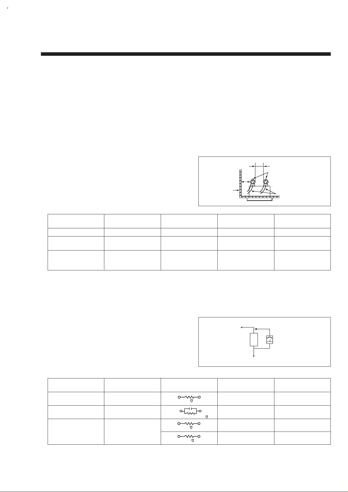
3. Clearance distance
When replacing primary circuit components, confirm
specified clearance distance (d), (d') between soldered
terminals, and between terminals and surrounding
metalic parts. See table below.
Table 1: Rating for selected areas
* Class II model only.
Note: This table is unofficial and for reference only. Be sure to confirm the precise values for your particular country and
locality.
4. Leakage current test
Confirm specified or lower leakage current between B (earth ground, power cord plug prongs) and externally exposed
accessible parts (RF terminals, antenna terminals, video and audio input and output terminals, microphone jacks,
earphone jacks, etc.)
Measuring Method: (Power ON)
Insert load Z between B (earth ground, power cord plug
prongs) and exposed accesible parts. Use and AC
voltmeter to measure across both terminals of load Z.
See figure 2 and following table.
Table 2: Leakage current ratings for selected areas
Note: This table is unofficial and for reference only. Be sure to confirm the precise values for your particular country and
locality.
Fig. 2
AC Line Voltage Region
Insulation Dielectric Clearance
Resistance Strength Distance (d), (d')
100V Japan ≥ 1 MΩ/500 VDC 1kV AC 1 minute ≥ 3 mm
110 to 130V
USA &
– – –
900V AC 1 minute ≥ 3.2mm
Canada
* 110 to 130 V Europe ≥ 4 MΩ/500 V DC 3 kV AC 1 minute ≥ 6 mm (d)
200 to 240 V Australia ≥ 8 mm (d')
(a: Power cord)
AC Line Voltage Region
Earth Ground
Load Z Leakage Current (i)
(B) to:
100V Japan ¡ ≤ 1m A rms
Exposed accessible
parts
110 to 130 V USA & ¡ ≤ 0.5 m A rms Exposed accessible
parts
¡ ≤ 0.7 m A peak Antenna earth
110 to 130 V Europe ¡ ≤ 2 m A dc terminals
200 to 240 V Australia ¡ ≤ 0.7 m A peak
Other terminals
¡ ≤ 2 m A dc
Fig. 1
1k
1.5k
1.5kµF
2k
50k
d
Primary circuit termimals
Chassis
d'
a
Exposed
accessible
part
Z
Earth Ground
power cord plug prongsB
AC Voltmter
(high impedance)
Page 4

TABLE OF CONTENTS
SECTION 1. CONTROLS AND FUNCTIONS..........................................................................................................2
SECTION 2. ELECTRICAL ADJUSTMENTS
2-1. SERVO CIRCUIT ADJUSTMENT METHOD..................................................................................................................... 3
2-2. AUDIO CIRCUIT ADJUSTMENT METHOD......................................................................................................................4
2-3. IF MODULE CIRCUIT ADJUSTMENT METHOD..............................................................................................................5
SECTION 3. TROUBLE SHOOTING FLOW CHART
3-1. POWER CIRCUIT.............................................................................................................................................................16
3-2. LOGIC CIRCUIT............................................................................................................. .................................................. 18
3-3. SERVO-SYSCON CIRCUIT.............................................................................................................................................20
3-4. AUDIO CIRCUIRT (NORMAL) .........................................................................................................................................25
3-5. AUDIO CIRCUIT (HI-FI)....................................................................................................................................................27
3-6. VIDEO CIRCUIT ...............................................................................................................................................................29
SECTION 4. CIRCUIT DIAGRAM
4-1. CONNECTION DIAGRAM (DV-F802 SERIES)................................................................................................................39
4-2. CONNECTION DIAGRAM (DV-F882 SERIES)................................................................................................................40
4-3. POWER CIRCUIT.............................................................................................................................................................41
4-4. SERVO-LOGIC CIRCUIT.................................................................................................................................................42
4-5. LOGIC CIRCUIT (DV-F802 SERIES)...............................................................................................................................43
4-6. LOGIC CIRCUIT II (DV-F882 SERIES) ............................................................................................................................44
4-7. HEADAMP CIRCUIT........................................................................................................................................................45
4-8. VIDEO CIRCUIT ...............................................................................................................................................................46
4-9. HI-FI AUDIO CIRCUIT......................................................................................................................................................47
4-10. PIF NICAM CIRCUIT......................................................................................................................................................48
4-11. PIF/MPX CIRCUIT..........................................................................................................................................................49
4-12. PIF CIRCUIT...................................................................................................................................................................50
4-13. OSD CIRCUIT ................................................................................................................................................................51
4-14. VPS/PDC CIRCUIT........................................................................................................................................................52
4-15. IN/OUT SW CIRCUIT I...................................................................................................................................................53
4-16. IN/OUT SW CIRCUIT II..................................................................................................................................................54
4-17.REMOCON CIRCUIT......................................................................................................................................................55
SECTION 5. VOLT AGE CHAR TS.................................................................................................................................56
SECTION 6. COMPONENTS LOCA TION GUIDE ON PCB BOTTOM VIEW........................................64
SECTION 7. DIS ASSEMBLY ........................................................................................................................................69
SECTION 8. ELECTRICAL P AR TS LIST..................................................................................................................73
1
Page 5
SECTION 1. CONTROLS AND FUNCTIONS
2
PLAY
STOP
POWER
EJECT
REC/OTR
REW
FF
=
POWER
EJECT
REC/OTR
REW
FF
PLAY
STOP
VIDEO L –AUDIO– R
CHANNEL
B.L.U.E D.I.A.M.O.N.D
RAPID REWIND SYSTEM
=
REC/OTR
POWER EJECT
õ CH.TRK.ö
PLAY
REW F.F
STOP
DV-F882 Series
DV-F802 Series
FRONT
REAR
EURO-AV
RF OUT
TV
CH.H CH.L
TEST
ON
OFF
ANT. IN
Page 6
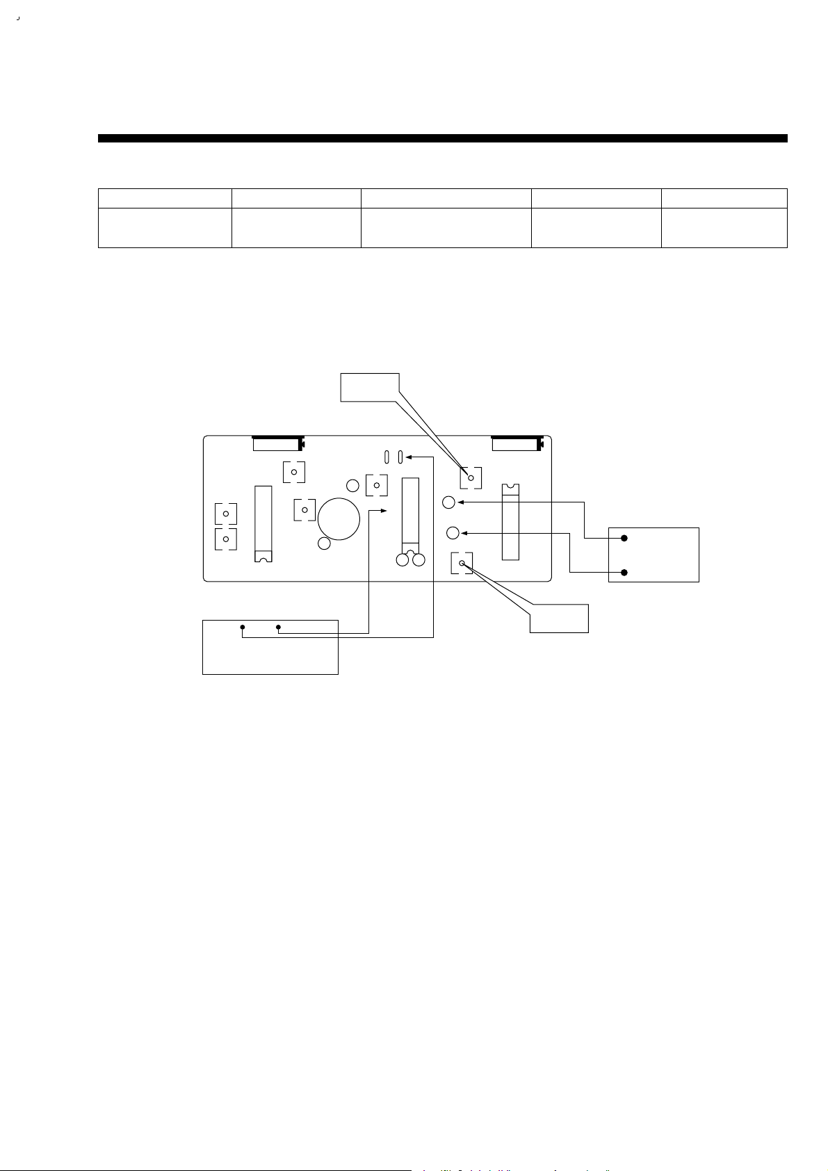
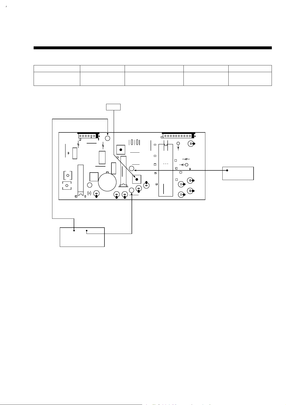
2-1. SERVO CIRCUIT ADJUSTMENT METHOD
1. PLAYBACK PHASE
• Connection Method
• Adjustment Procedure
1) Play back the test tape.(DP-2)
2) Set the oscilloscope to the CHOP mode. Connect CH1 to the SW PULSE (PT01 PIN ¤Ø).
3) Insert PATH JIG and Press “REC” button on the remote controller.
4) Check the position of the V-sync from the rising edge of the SW pulse.
(Standard: 6.5H±0.5H)
SECTION 2. ELECTRICAL ADJUSTMENT
Adjustment Parts Checking Point Measuring Equipment Mode Test Tape
JPT01
DP-2
Check
PT01 PIN ¤Ø
Oscilloscope Play
Modulator
JPT01
CH-1
OSCILLOSCOPE
CH-2
PT01
TOP VIEW
PATH JIG
6
3
Page 7
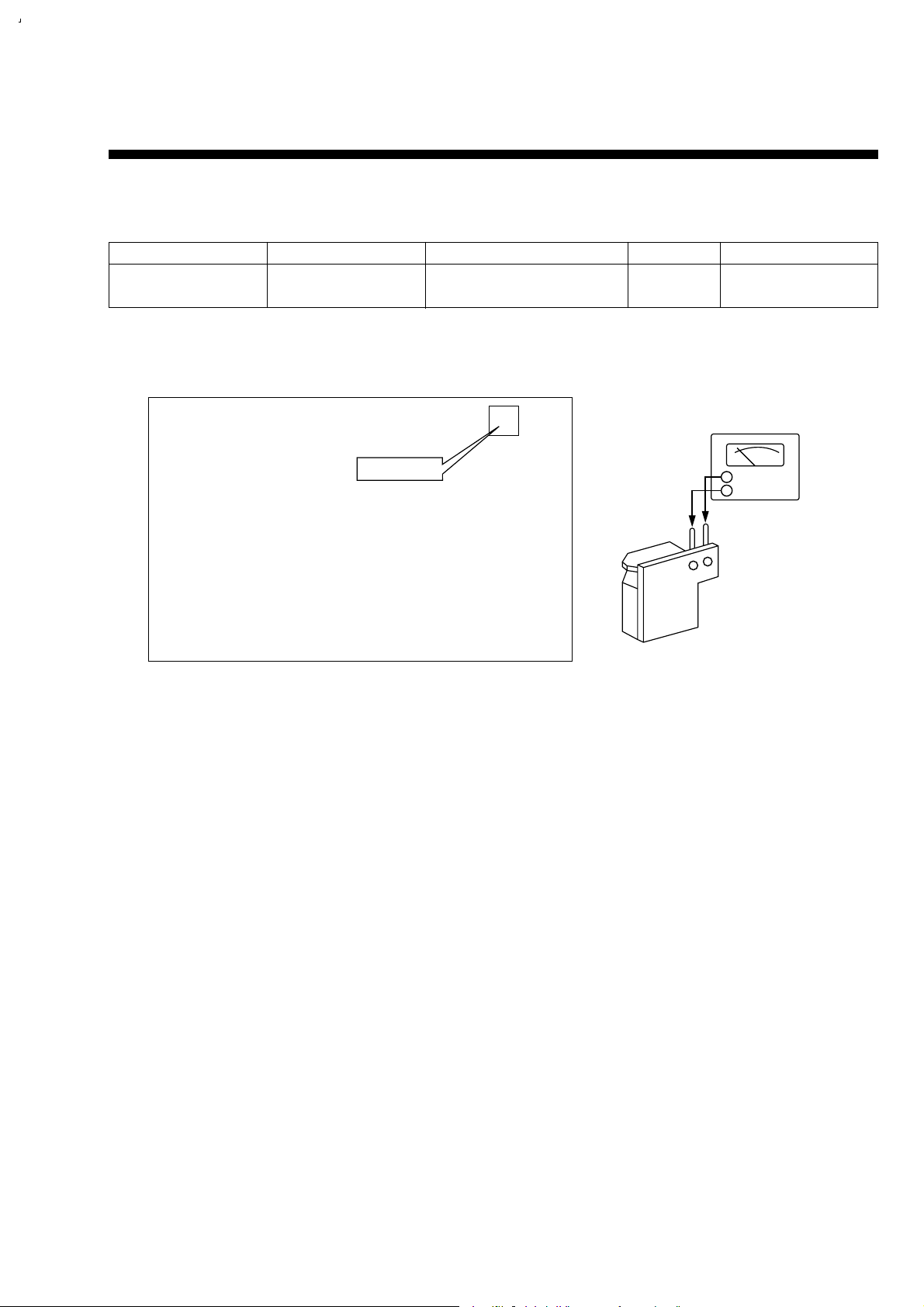
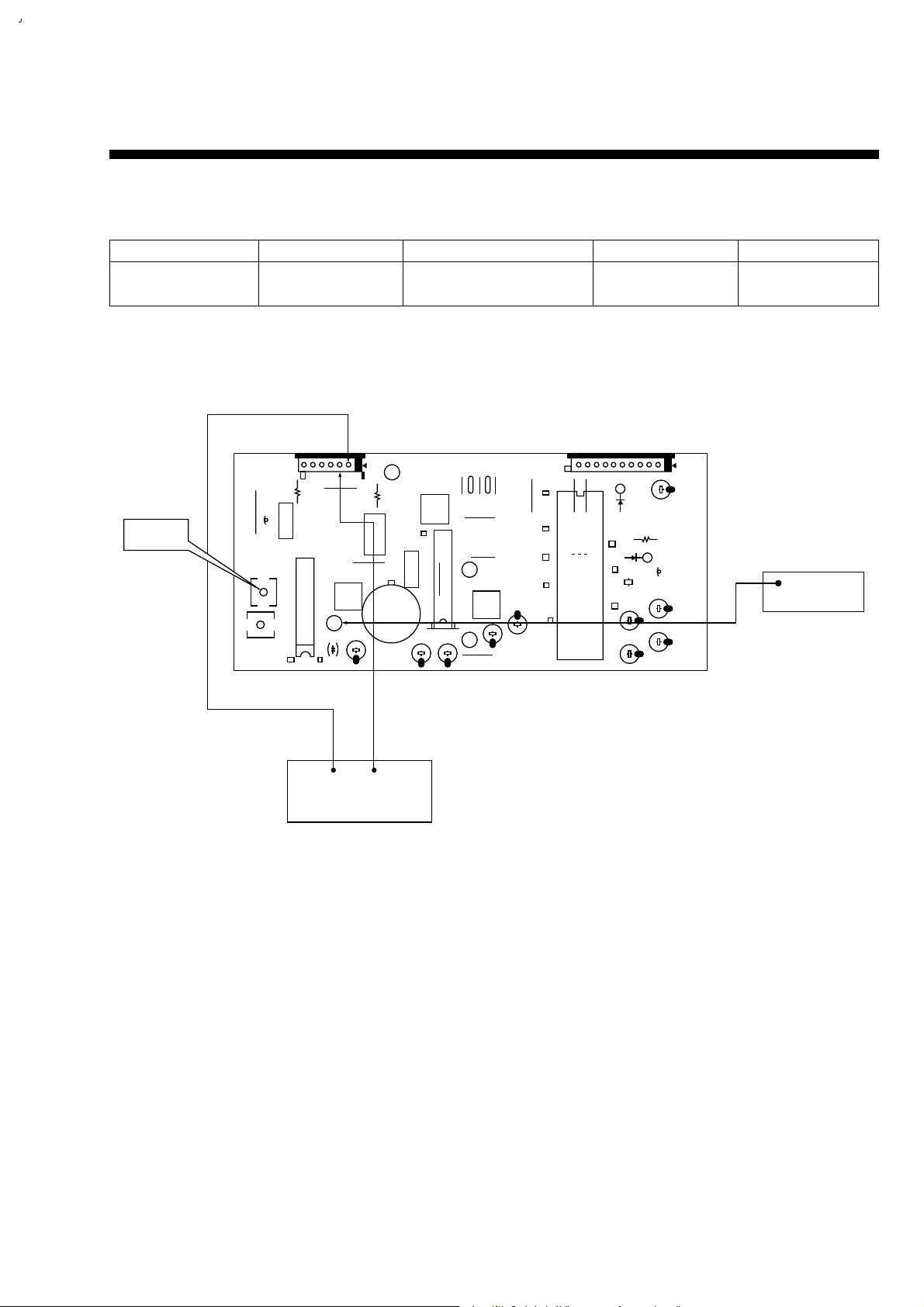
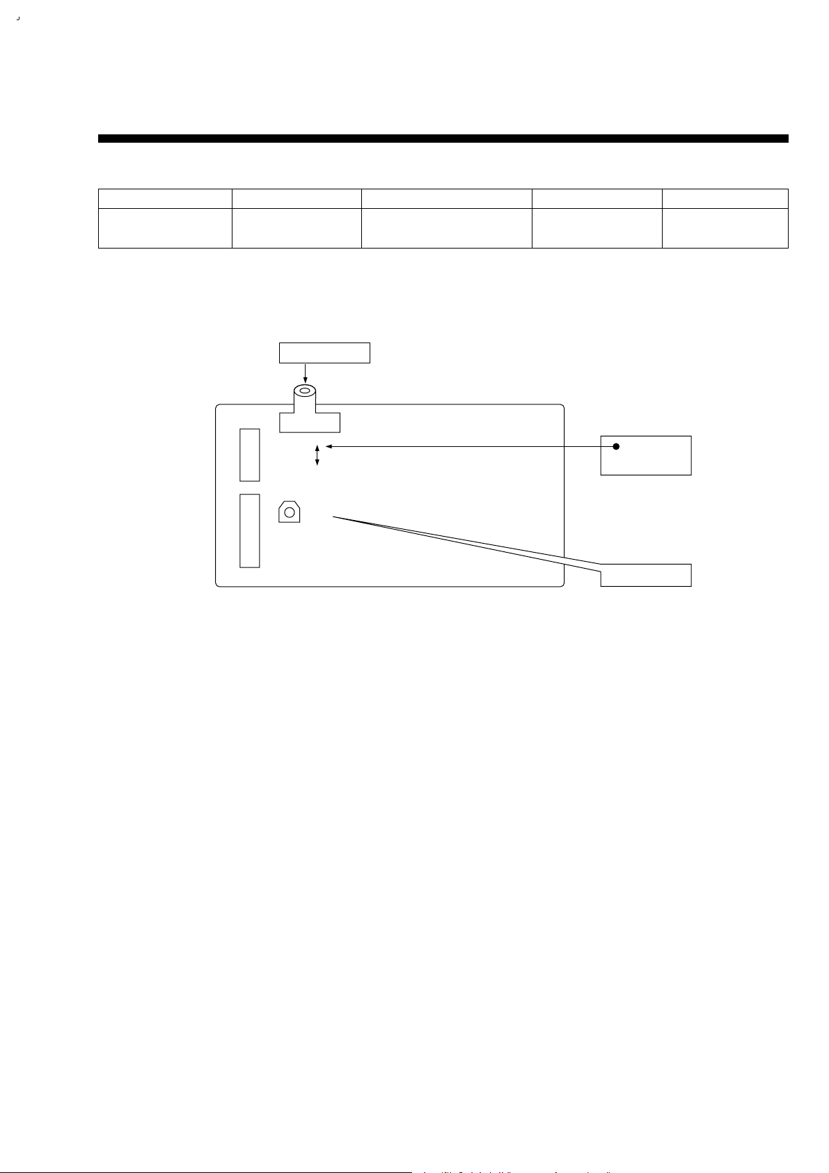
2-2. AUDIO CIRCUIT ADJUSTMENT METHOD
1. AUDIO RECORD BIAS
• Connection Method
• Adjustment Procedure
1) Set the TV/LINE to LINE mode.
2) Set the input to open mode
3) Connect the Audio level meter to both TP1 and TP2
4) After inserting a blank tape, record in SP mode.
5) Adjust R290 to obtain 3.0 mVrms.
4
TOP VIEW
R290
3.0mVrms
+
–
A/CHEAD
TP2
(–)
TP1
(+)
Audio LEVEL METER
S/N: 97P65064HA
HEAD AMP PCB
Adjustment Parts Checking Point Measuring Equipment Test Tape Input Signal
R290
A/C Head PCB
Audio level meter Rec None signal
TP1(+), TP2(-)
Page 8
5
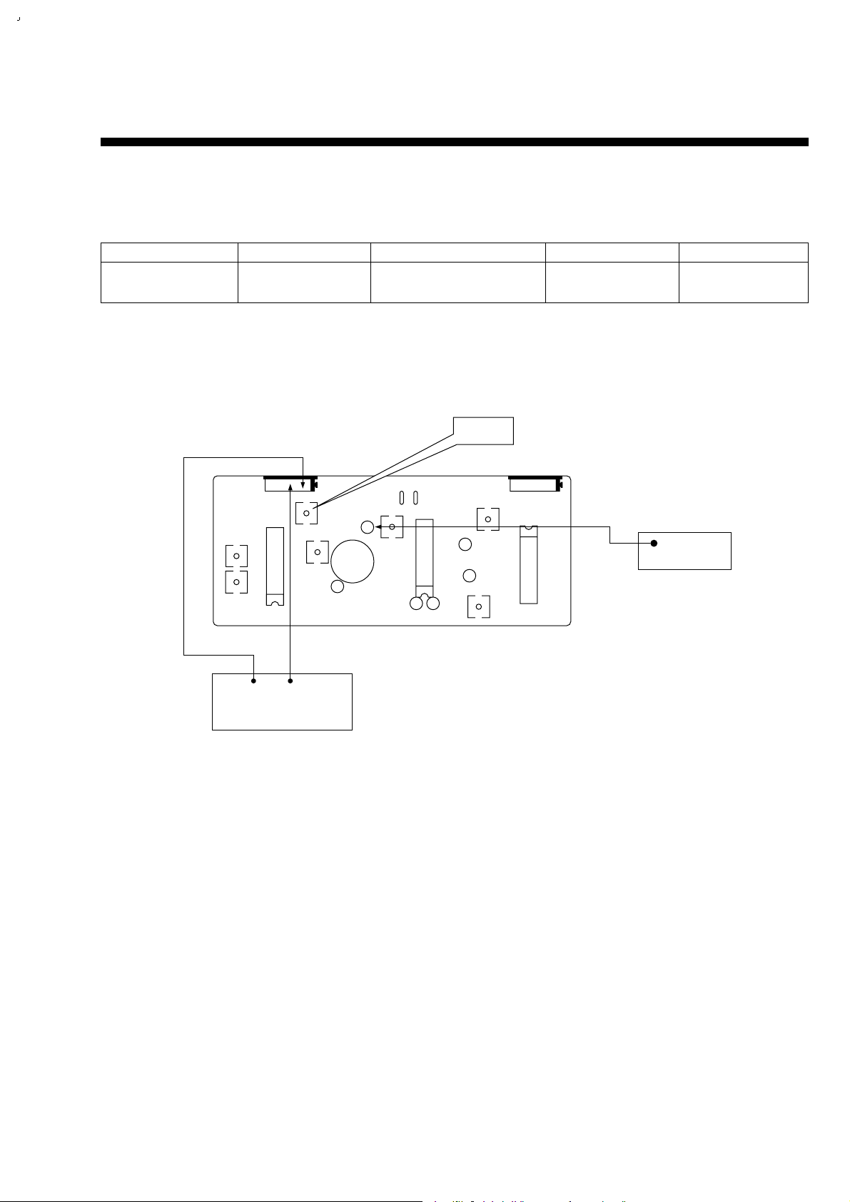
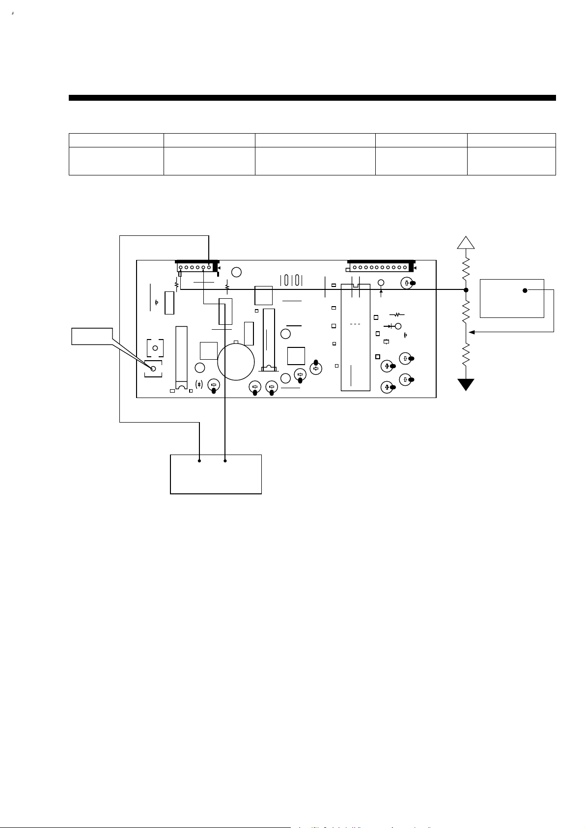
2-3. IF MODULE CIRCUIT ADJUSTMENT METHOD
2-3-1. P AL B/G 2 CARRIER SYSTEM
1. 32.4MHz TRAP
• Connection Method
• Adjustment Procedure
1) Supply +12V to pin No.1, and GND to Pin No 2. of 102
2) Connect the signal generator output to pin 3 and GND to pin 2 of P102.
3) Connect the oscilloscope to TP1.
4) Adjust L101 until the level of signal becomes minimum.
P102
L104
L105
IC101
#3
#2
L101
TP1
L108
TP2
L103
Z101
TP6 TP7
IC102
TP3
L109
P101
IC103
L110
TP4
minimum
CH-1
Oscilloscope
GND
OUT
#3
PIF PCB (Component Side)
SIGNAL
GENERATOR
fc: 32.4 MHz (No modulation)
Output Level: 80dBµV (75Ω loaded)
#2
Adjustment Parts Checking Point Measuring Equipment Condition of Adj. Input Signal
L101 TP1
Oscilloscope
EE Mode
Refer to the
Signal Gen followings
Page 9
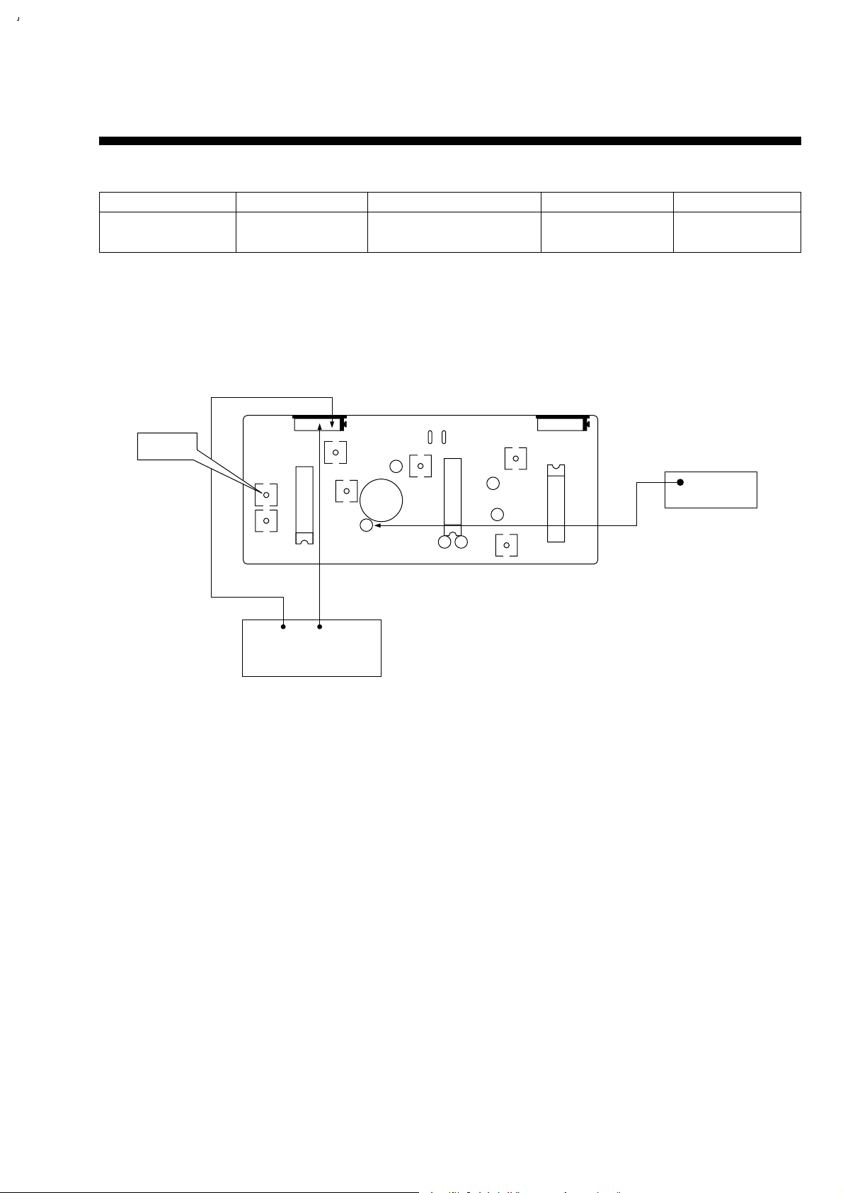
2. PIF COIL
• Connection Method
• Adjustment Procedure
1) Supply +12V to pin No.1, and GND to Pin No 2. of 102
2) Connect the signal generator output to pin 3 and GND to pin 2 of P102.
3) Connect the oscilloscope to TP2.
4) Adjust L104 to obtain the minimum DC voltage of TP2.
6
P102
L104
L105
IC101
#3
#2
L101
TP1
L108
TP2
L103
Z101
TP6 TP7
IC102
TP3
L109
P101
IC103
L110
TP4
CH-1
Oscilloscope
GND
OUT
minimum
#3
PIF PCB (Component Side)
SIGNAL
GENERATOR
fc: 38.9MHz
Output Level: 80dBµV (75Ω loaded)
#2
Adjustment Parts Checking Point Measuring Equipment Condition of Adj. Input Signal
L104 TP2
Oscilloscope
EE Mode
Refer to the
Signal Gen followings
Page 10
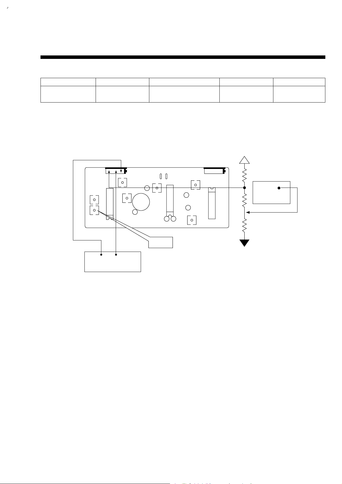
3. AFT COIL
• Connection Method
• Adjustment Procedure
1) Supply +12V to pin No.1, and GND to Pin No 2. of 102
2) Connect the signal generator output to pin 3 and GND to pin 2 of P102.
3) Connect the Test circuit to pin No. 7 of P102
4) Connect the oscilloscope to “A” point and GND
5) Adjust L105 to obtain 2.3V DC Voltage at the "A" point
7
P102
L104
L105
IC101
#3
#2
L101
TP1
L108
TP2
L103
Z101
TP6 TP7
IC102
TP3
L109
P101
IC103
L110
TP4
2.3±0.5V
CH-1
Oscilloscope
GND
OUT
#3
#7
PIF PCB (Component Side)
#2
#7
SIGNAL
GENERATOR
fc: 38.9MHz, fm: 15.625KHz (30% AM Modulation)
Output level: 80dBµV (75Ω loaded)
43kΩ
33kΩ
18kΩ
"A"
Vcc+12V
GND
(Test circuit)
Adjustment Parts Checking Point Measuring Equipment Condition of Adj. Input Signal
L105 “A” point
Oscilloscope
EE Mode
Refer to the
Signal Gen. followings
Page 11
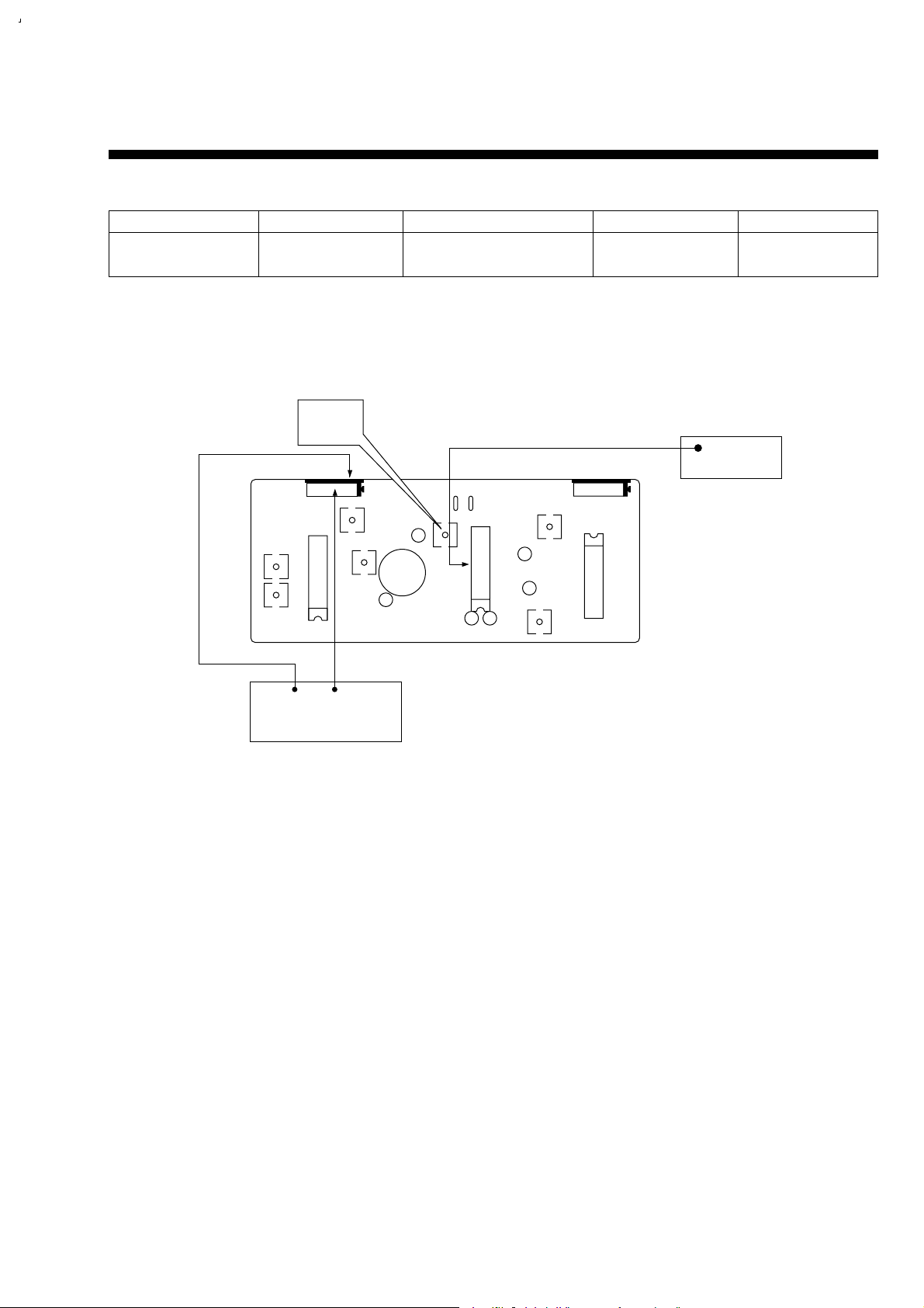
4. SOUND CARRIER
• Connection Method
• Adjustment Procedure
1) Supply +12V to pin No. 1, and GND to pin No. 2 of P102
Supply +5V to pin No. 3, and GND to pin No. 1 of P101
2) Connect the signal generator output to pin 3 and GND to pin 2 of 102.
3) Connect the oscilloscope to pin NO.15 of IC102.
4) Adjust L108 to obtain the minimum Noise, minimum Level of pin NO.15 of IC102.
8
P102
L104
L105
IC101
L101
TP1
L108
TP2
L103
Z101
TP6 TP7
IC102
TP3
L109
P101
IC103
L110
TP4
minimum
noise
level
CH-1
Oscilloscope
GND
OUT
PIF PCB (Component Side)
SIGNAL
GENERATOR
fc: 38.9MHz, fm: 15.625KHz (30% AM Modulation)
Output level: 80dBµV (75Ω loaded)
#3
#2
#2
Adjustment Parts Checking Point Measuring Equipment Condition of Adj. Input Signal
L190 IC102 #15
Oscilloscope
EE Mode
Refer to the
Signal Gen. followings
Page 12
5. LEFT, RIGHT SOUND
• Connection Method
• Adjustment Procedure
1) Supply +12V to pin No. 1, and GND to pin No. 2 of P102
Supply +5V to pin No. 3, and GND to pin No. 1 of P101
2) Connect the signal generator output to pin NO.15 of IC102 and GND.
3) Connect the oscilloscope to TP3, TP4.
4) Adjust L109 to obtain the maximum level of TP3.
5) Adjust L110 to obtain the maximum level of TP4.
9
P102
L104
L105
IC101
L101
TP1
L108
TP2
L103
Z101
TP6 TP7
IC102
TP3
L109
P101
IC103
L110
TP4
CH-1
Oscilloscope
CH-2
GND
OUT
LEFT
RIGHT
PIF PCB (Component Side)
SIGNAL
GENERATOR
fc: 5.5MHz (LEFT) fm: 1KHz (50KHz FM Modulation)
5.74MHz (RIGHT)
Output level: 100dBµV (75Ω loaded)
GND
#15
#15
Adjustment Parts Checking Point Measuring Equipment Condition of Adj. Input Signal
L109 (LEFT) TP3 Oscilloscope
EE Mode
Refer to the
L110 (RIGHT) TP4 Signal Gen. followings
Page 13

6. RF AGC
• Connection Method
• Adjustment Procedure
1) Turn on the VCR, Tuning CH21 (471.25MHz)
2) Connect the signal generator output to ANT INPUT of RF 102 (Modulator)
3) Connect the oscilloscope to JPT02
4) Adjust R190 to obtain 6.0±0.2V DC.
10
CH-1
Oscilloscope
MAIN PCB
RF Signal : PAL B/G (Color Bar or 100% white)
CH : 21 CH (471.25MHz)
UHF BAND
RF102
RF101 JPT02
RF103
R190
6.0±0.2V
Input Level : 70±1 dBµV
(75Ω Loaded)
RF OUT PM5418
Modulator ANT IN
Adjustment Parts Checking Point Measuring Equipment Condition of Adj. Input Signal
R190 JPT02
Oscilloscope
EE Mode
Refer to the
PM5418 Gen. followings
Page 14
2-3-2. P AL B/G, I NICAM SYSTEM
1. PIF COIL (NICAM)
• Connection Method
• Adjustment Procedure
1) Supply +12V DC to Pin No.1, and GND to Pin No 2. of 102
2) Connect the signal generator output to pin 3 and GND to pin 2 of P102.
3) Connect the oscilloscope to TP2.
4) Adjust L104 to obtain the minimum DC voltage of TP2.
11
97P651111A
P102
P101
TP1
CH-1
Oscilloscope
SIGNAL
GENERATOR
GND
OUT
fc: 39.5MHz (I)
38.9MHz (B/G)
Output Level: 80dBµV (75Ω loaded)
minimum
#2
#3
R103
J1
L104
L105
Z101
C107
C106
IC101
TP2
J4
C115
TP3
J19
IC102
L108
J7
J12
J13
J15
C181
D101
R163
L112
X102
30 27
D102
C153
C182
C176C178
TP4
J11
J10
J9
J8
IC104
J6
L103
Adjustment Parts Checking Point Measuring Equipment Condition of Adj. Input Signal
L104 TP2
Oscilloscope
EE Mode
Refer to the
Signal Gen. followings
Page 15
2. AFT COIL
• Connection Method
• Adjustment Procedure
1) Supply +12V DC to Pin No.1, and GND to Pin No 2. of 102
2) Connect the signal generator output to pin 3 and GND to pin 2 of P102.
3) Connect the test circuit to pin No.7 of P102
4) Connect the oscilloscope to “A” point and GND
5) Adjust L105 to obtain 2.3V DC voltage at the "A" point
12
97P651111A
P102
P101
TP1
SIGNAL
GENERATOR
GND
OUT
fc: 39.5MHz (I)
fc: 38.9MHz (B/G)
fm: 15.625KHz (30% AM MODULATION)
Output Level:80 dBµV (75Ω loaded)
2.3±0.5V
#2
#3
R103
J1
L104
L105
Z101
C107
C106
IC101
L103
TP2
J4
C115
TP3
J19
IC102
L108
J7
J14
J12
J13
J15
C181
D101
R163
L112
X102
30 27
D102
C153
C182
C176C178
TP4
J11
J10
J9
J8
IC104
J6
CH-1
Oscilloscope
#7
43kΩ
33kΩ
18kΩ
(Test circuit)
Vcc+12V
GND
"A"
Adjustment Parts Checking Point Measuring Equipment Condition of Adj. Input Signal
L105 “A” point
Oscilloscope
EE Mode
Refer to the
Signal Gen. followings
Page 16
3. SOUND CARRIER (NICAM)
• Connection Method
• Adjustment Procedure
1) Supply +12V DC to Pin No.1 and GND to pin No. 2 of P102
2) Supply +5V DC to Pin No.3 GND to Pin No. 1 of P101.
3) Connect the signal generator output to pin 3 and GND to pin 2 of p102
4) Connect the oscilloscope to TP3.
5) Adjust L108 to obtain the minimum noise, minimum level of TP3.
13
97P651111A
P102
P101
TP1
CH-1
Oscilloscope
SIGNAL
GENERATOR
GND
OUT
fc: 39.5MHz (I)
38.9MHz (B/G)
fm: 15.625KHz (30% AM MODULATION)
Output Level:80 dBµV (75Ω loaded)
minimum
noise
level
#3
R103
S2
J3
J1
L104
L105
Z101
C107
C106
IC101
L103
TP2
J4
C115
J19
IC102
L108
J7
J14
J12
J13
J15
C161
D101
R163
L112
X102
30 27
D102
C155
C182
C176C178
TP4
J11
J10
J9
J8
IC104
J6
TP3
#3#2
#2
Adjustment Parts Checking Point Measuring Equipment Condition of Adj. Input Signal
L108 TP3
Oscilloscope
EE Mode
Refer to the
Signal Gen followings
Page 17
4. 5.5 (6.0) MHz SOUND
• Connection Method
• Adjustment Procedure
1) Supply +5V DC to Pin No.3 GND to Pin No. 1 of P101.
2) Connect the signal generator output to TP3 and GND to TP1.
3) Connect the oscilloscope to TP4.
4) Adjust L109 to obtain the maximum level of TP4.
14
97P651111A
P102
P101
TP1
CH-1
Oscilloscope
SIGNAL
GENERATOR
GND
OUT
fc: 6.0MHz (I)
5.5MHz (B/G)
fm: 1KHz (50kHz FM MODULATION)
Output Level: 100dBµV (75Ω loaded)
L109
#3
R103
J1
L104
L105
Z101
C107
C106
IC101
L103
TP2
J4
C115
J19
IC102
L108
J7
J14
J12
J13
J15
C181
D101
R163
L112
X102
30 27
D102
C153
C182
C176C178
TP4
J11
J10
J9
J8
IC104
J6
TP3
Adjustment Parts Checking Point Measuring Equipment Condition of Adj. Input Signal
L109 TP4
Oscilloscope
EE Mode
Refer to the
Signal Gen followings
Page 18
5. RF AGC
• Connection Method
• Adjustment Procedure
1) Turn on the VCR. Tuning CH21 (471.25MHz)
2) Connect the signal generator output (PM5418 pattern Gen) to ANT INPUT of RF102 (Modulator)
3) Connect the oscilloscope to JPT02
4) Adjust R190 to obtain 6.0±0.2V DC.
15
CH-1
Oscilloscope
MAIN PCB
RF Signal : PAL B/G (Color Bar or 100% white)
CH : 21 CH (471.25MHz)
UHF BAND
RF102
RF101 JPT02
RF103
R190
6.0±0.2V
Input Level : 60 dBµV (I)
63 dBµV (B/G)
(75 ohm Loaded)
RF OUT PM5418
Modulator ANT IN
Adjustment Parts Checking Point Measuring Equipment Condition of Adj. Input Signal
R190 JPT02
Oscilloscope
EE Mode
Refer to the
PM5418 Gen followings
Page 19
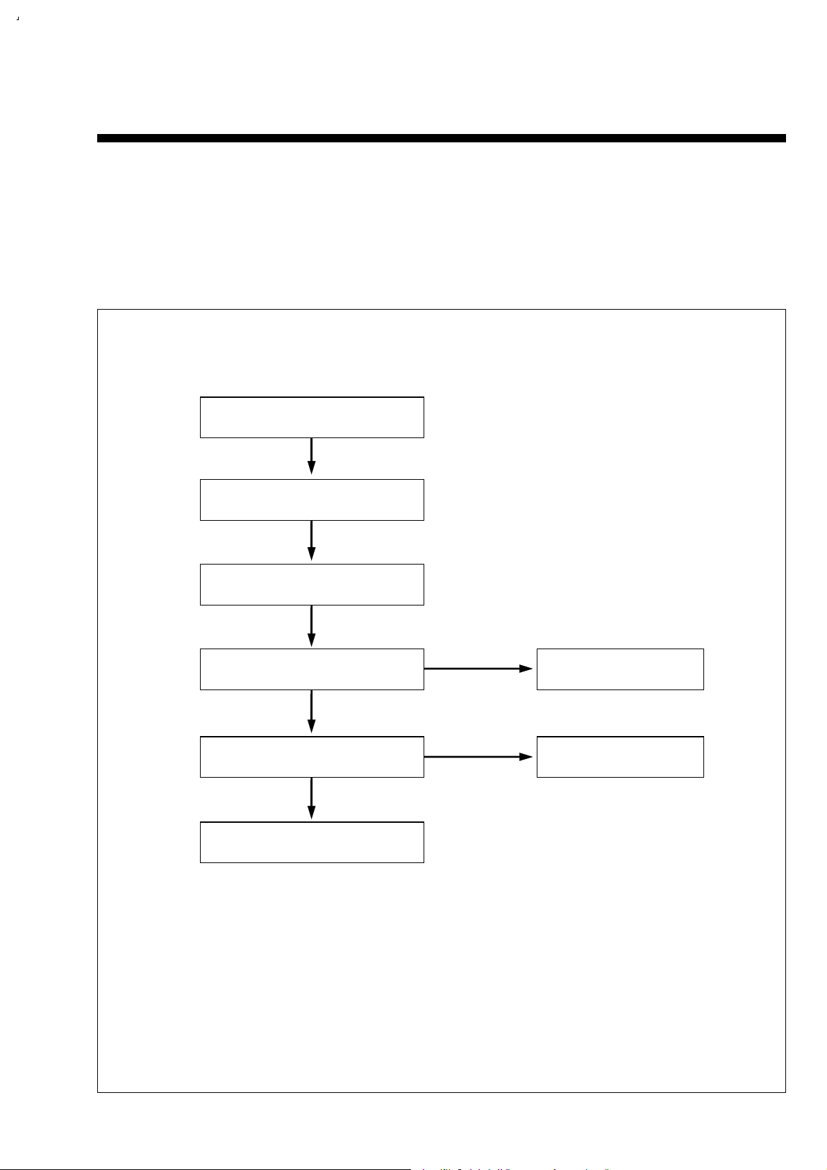
SECTION 3. TROUBLE SHOOTING FLOW CHAR T
3-1. POWER CIRCUIT
• When change the parts which are out of order, first, remove the power plug from the socket and then discharge the
voltage across between both terminals of C807. (Use an external scores of KΩresistance)
• When check the primary circuit by using the oscilloscopes insulate the oscilloscope surely. (Use the isulating
transformer) and must connect GND into the primary GND), (But there is no connection when check the secondary
circuit).
• When change IC801, check FUSE and Cement resistance surely.
16
Prepare the instrument
connecting the insulating trans.
Check F801 FUSE
Is voltage applied to D801?
Is voltage applied to the
both terminals of C807?
Check power module
Check D801, L801 & L802
Check R802
NO
NO
YES
YES
YES
YES
YES
NO output Voltage
A. CHECKING THE PRIMARY CIRCUIT.
Page 20
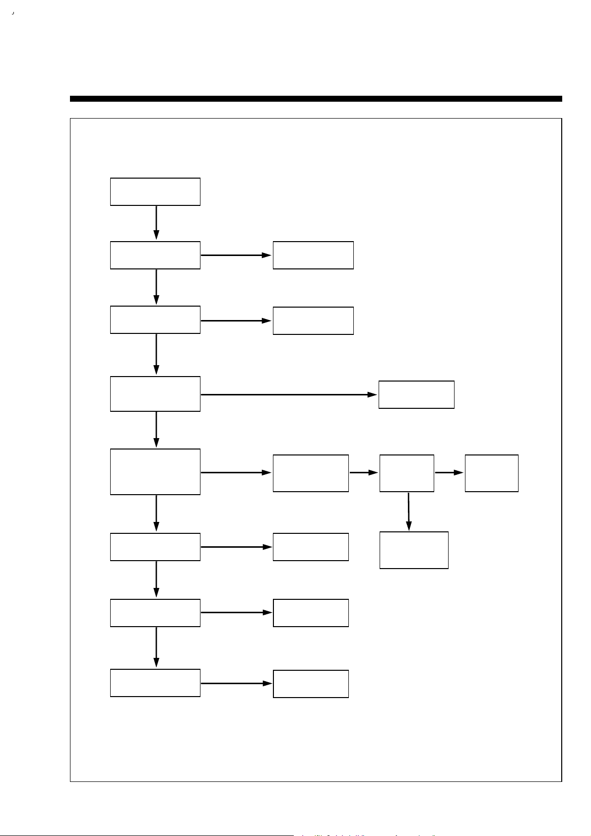
17
No Voltage
output
Is voltage supplied
Via CN11?
The voltage of #1 of
IC11 is 5.7V and stable
The voltage of #1 of IC11
fluctuate
in 4.8V~5.7V
Measure resistance
between GND of CN21
and each terminal
of CN21
The 12DC of each
wire of T11 is ok
Primary parts is ok
Secondary parts ok
Change T11
Change parts
out of order
YES
NO
YES
Resistance >> 100
YES
YES
NO
NO
Check F801, L801,
L802, D802
NO
Check the secondary
circuit
YES
Check the pattern
and T11, L12, IC11
NO
Terminal open and
measure the output
Voltage
Change parts
out of order
NO
The voltage
is ok
Check the
parts outside
module
Check the Diode,
Condenser inside
Module
NO
YES
B. POWER MODULE (M801) CHECK
Page 21
3-2. LOGIC CIRCUIT
18
Digitron does
not operate.
Is +5V supplied to
pin of IC701?
8
Is -28V supplied to
pin of IC701?
11
Are -20 and -16.5V
supplied to pin and
of G701?
1
35
Are CLK signals
supplied to pin ), I
and i, of IC701?
Is 5V at pin of
IC701?
7
Check X701
Check IC701
and change.
check power circuit
Is +5.8V supplied
from D713 cathod
Is -28V at D650
anode
Check D814 and
primary power circuit.
Check the connector
and pattern.
Check the power
module
Check IC601
Change
Change
YES
YES
YES
YES
YES
YES
NO
NO
NO
NO
NO
NO
NO
NO
YES
A.
Page 22
19
Digitron is lit keys do
not operate.
Is each key pulse
applied to pin ,
and of IC701?
2 3
12 13
Check key matrix
circuit.
Check the pin serial of
pin , ~ of IC701.
19 22 24
Power compensation
does not operated.
When mains is
unplugged is 3.6V at
pin and of IC601?
26 81
Is signal applied to
pin and of IC601?
42 43
Is 5V at pin of IC601
37
Check IC601
Check C623
Check x602
Check reset circuit
IC604
NO
YES
YES
YES
YES
NO
NO
NO
B.
C.
B.
C.
Page 23
20
91
The voltage of pin
of IC601 is not
changed.
Is CTL pulse input
to pin and of
IC601
71 72
73
Check and
re-adjust the
Path of Deck.
Check circuit
adjacent to IC601
Check C508, C509
check R518
and C511
Check IC601
YES
YES
YES
YES
YES
YES
YESNO
NO NO
NO
NO
NO
A.
Playback picture
is not good.
Noise appears
although adjusting
tracking.
Is CTL pulse out
from pin of IC601.
Noise shakes up
and down on the
screen.
Adjust
tracking
CTL HEAD height is
normal and there is
not dust.
Adjust the HEAD
height and remove
dust
Noise appears
although change
cassette tape.
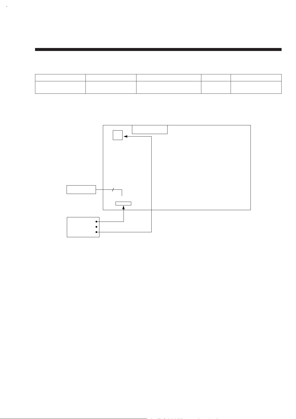
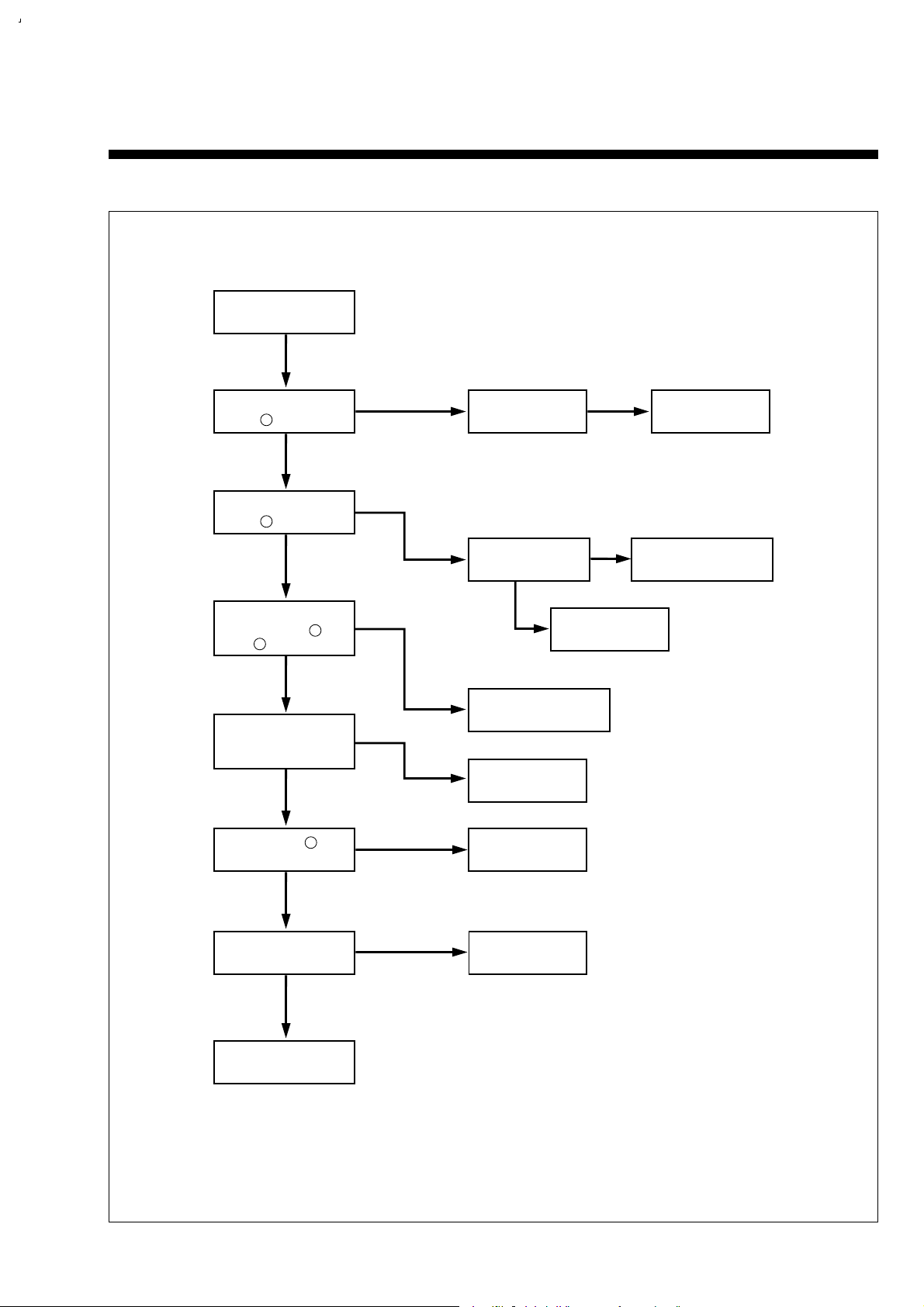
3-3. SERVO SYSCON CIRCUIT
Page 24
21
Playback picture
is not good.
Noise appears
on the screen
on the whole.
Is Enve.wavefrom
supplied to at pin of
PT01
4
Are SW pulse and
HA SW applied to
HeadAmp circuit?
Check video circuit.
Auto stop during
playback
Is Reel pulse
applied to pin and
of IC601?
5
6
Check flow A
Is SW pulse supplied
from pin of IC601?
18
Check D.PG input
and connector.
Check pattern
Check connector, Head
Amp and Head dust.
Change head
Check reel sensor.
Is D.FG applied to
pin of IC601
Check connector
D.FG circuits.
Check IC601
YES
NO
YES
YES
YES
YES
YES
YES
NO NO
NO
NO
NO
YES
NO
67
B.
C.
Page 25
22
Drum M/T loading stops.
Is Motor 12V supplied?
Is pin D.FG of
IC601 supplied.
Is pin D.PWM (pin )
of IC601 supplied?
Check connector
and Motor.
Is the input of pin
of P501 2V-3.5V?
Is pin of P601 2.5V
Is pin (C.PWM)
of IC601 Supplied?
Check connector
and Motor
67
4
1
18
3
Check Q851 of
power circuit.
Check C505, R506, R507
and C516
Check IC601
Check power circuit.
Check circuit of R510,
R511, R512.
Check R508, R509
Check IC601
YES
YES
YES
YES
YES
YES
YES
YES
NO
NO
NO
NO
NO
NO
NO
Capstan M/T loading stops.
Is Motor 12V supplied?
D.
E.
Page 26
23
Drum M/T and Capstan M/T rotate
at regular speed. (In REC mode)
Is C. Sync applied to
pin of IC601?
93
Check Motor.
Check C. Sync of
VIDEO IC and Pattern
Emergency mode when plugging
(Power cord)
Is EVER 5V supplied?
Does X601 crystal osciliate?
Do S/DATA, CLK and RDY
Signals of IC601 exchange
with IC701
Is CAM SW DATA Correct?
Check IC602.
Check IC 601.
Check power circuit.
Check IC601 and X601.
Check IC701 when S.RDY Signal
is supplied.
Check IC601 when S.RDY Signal
is not supplied.
Recheck connector
and CAM SW contact.
NO
YES
YES
YES
YES
YES
YES
NO
NO
NO
NO
NO
F.
G.
Page 27
24
Cassette is not
inserted.
Is Motor 12V supplied?
Check Q851 of power
circuit
CAM DATA is changed
when CST IN?
Is 5V applied to
pin of IC602 when CST IN?
4
Chek IC602
Check connector. Check DECK part.
Is 5V supplied at
pin of IC601?
Check PATTERN
45
Check IC601
H.
NO
YES
YES
YES
NO NO
NO NO
YES
Page 28

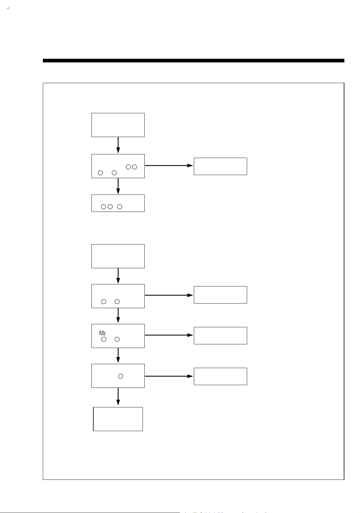
3-4. AUDIO CIRCUIT (NORMAL)
25
No sound in the playback mode.
Is the output at pin “, ‘
of IC201?
Is 12V applied to pin a
of IC201?
Check power circuit.
Is 5V applied to pin 3, g
of IC201?
Is pin of IC201 10V
4
Is there Audio output
pin of IC201?
29
Is pin of IC202 GND?
2
Check Pattern
and AC Head.
Chack IC601.
Check IC202
NO
YES
NO
YES
YES
YES
YES
NO
NO
NO
A. Troubleshooting of PB mode
Is 5V and clock data applied to pin 4, 5 of IC201?
YES
NO
Page 29

26
Is signal input into
pin @, # of IC201 in TV mode
Is signal input into pin ^, & of
IC201 in LINE mode
Is 5V applied to pin $
of IC202?
Is the signal applied to
pin @ of IC202?
Does T230 oscillate?
Check SCART jack
Check SYSCON
Is the signal applied to
pin T of IC201?
Is the voltage above 10V
at pin of T230
Check Q232
collector:above 10V
Base:0V
Check T230
Is record current
3.0mVms?
Is pin of IC201 0V?
35
Clean HEAD.
Asjust Record current.
Check IC201.
Check IC201.
Check IC201.
NO
YES
YES
YES
YES
YES
YES
NO
NO
NO
YES
NO
NO
NO
NO
YES
3
B. Troubleshooting of REC mode
No sound in the playback
mode after recording
Check PIF circuit
Check IC202.
Check IC201.
NO
NO
Page 30

3-5. AUDIO CIRCUIT (Hi-Fi)
27
No sound in the E-E mode
Check
POWER circuit
NO
Is 12V applied to pin a
of IC201?
A. Troubleshooting of E-E mode
Is 5V applied to pin 3
g, of IC201?
Is signal input into
pin @, # of IC 201
in TV mode?
Is signal input into
pin ^, & of IC 201
in LINE mode?
Check
PIF circuit
NO
Check
SCART jack
NO
Is 5V and clock data
applied to pin 4, 5
of IC201?
Check SYSCON
NO
Is there output at
pin “, ‘ of IC201?
NO
Change IC201
NO
Check Q203 base; 5V
collector; 0V
Check SYSCON
NO
Check Q200, Q201, Q202
base; 0V
Change Q200, Q201, Q202
NO
Check SCART Jack
YES
YES
YES
YES
YES
YES
YES
YES
Page 31

28
No Hi-Fi Sound
in playback mode
Is the ENVE level of
JPT02 more than 120mVp-p?
Is A.SW PULSE input into
pin of IC201?
Is 5V and clock data applied
to pin , of IC201?
Is signal input into pin ,
of IC201
Check pin of IC601
Is there output at
, of IC201?
Check CK13,CM13
Is there output at
pin , of IC201
SCART JACK check
Change IC201
YES
YES
YES
YES
YES
NO
NO
NO
NO NO
B. Troubleshooting of Hi-Fi PB and REC mode
NO
Check the ICB01
of PRE-AMP circuit
61
20
14 15
Check IC601
51 64
52 63
21 22
Page 32

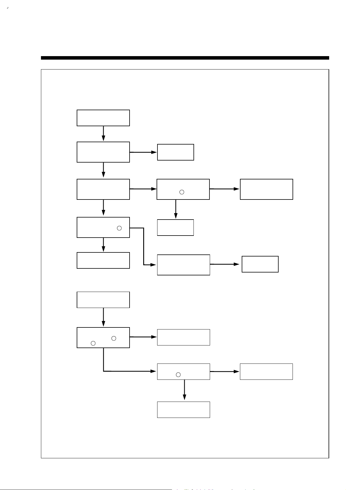
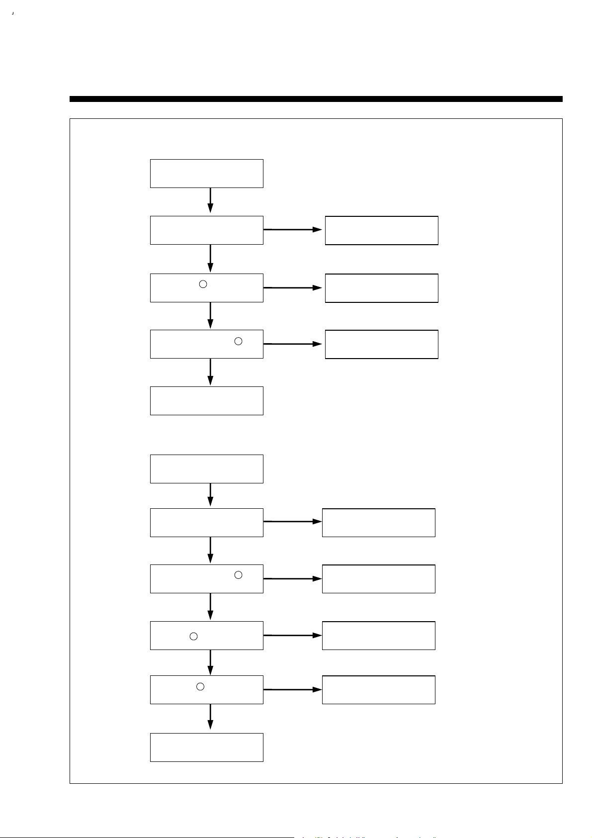
3-6. VIDEO CIRCUIT
29
Is video signal input
into pin and of IC151?
12 13
Is E12V supplied at
pin of IC151
16
Is signal output from
pin of IC151?
14
Is signal input into
pin of IC301?
12
Is signal output from
pin of IC301?
16
Check PIF circuit
and A/V jack.
Check ever 12V
Check IC151 and
adjacent circuit.
Check connector,
PCB pattern
Is 5V supplied to pin
and of IC301?
34
13
Check
power circuit
Check IC301
pin EE
Check
IC601 pin
29
Change IC301
Is signal input from
ICS01 pin?
10
Is signal output from
ICS01 pin?
8
Check pattern,
connector and Q303.
Check OSD circuit
Check RF out Check Line out
YES
YES
YES
YES
YES
YES
YES
YES
NO
NO
NO
NO
NO NO
H
L
A.EE MODE Picture N.G
NO
YES
Page 33

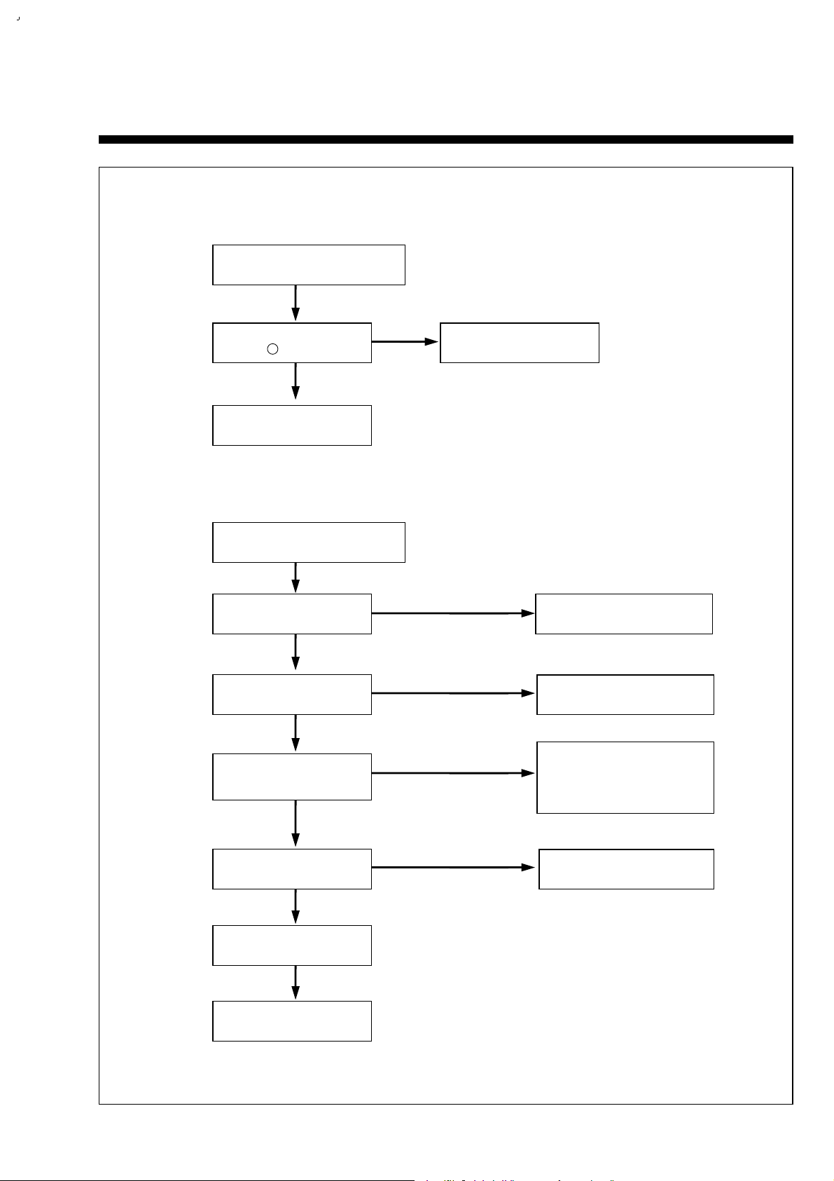
30
Is 5V supplied at ICS01 and pins?
Check oscillation of ICS01 ,
Check serial data (ICS01 pin)
Change ICS01 and check OSD circuit.
Check ON/OFF 5V
Check XS01 (17.7MHz)
Check IC601.
3
16 17
4 5
20
Is 5V supplied at
ICS01 and pins?
7
Is serial data input into
ICS01 pin
3 4 5
Check oscillation
of ICS01
16 17
Change ICS01
Check ON/OFF 5V
Check IC601.
Check LS01,CS01
and CS02.
YES
YES
NO
NO
NO
NO
NO
NO
YES
YES
YES
B . OSD Character N.G
20 7
C. OSD Character N.G
Page 34

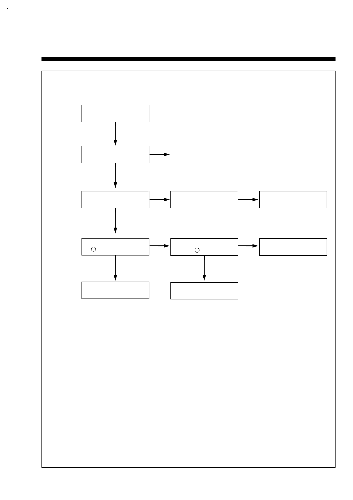
31
Is the video signal from pin of IC151
fed to pin of IC301?
NO
YES
Check C158 and pattern
14
12
Is ON/OFF 5V supplied to pin and
pin of IC301 at 5volts?
NO
YES
Check ON/OFF 5V
13
34
Is EE(L) supplied to anode of
D302 at zero volt?
NO
YES
Check EE(L)
Is the down-converted colour signal
obtained from pin of IC301?
NO
YES
Change IC301
38
Is the down-converted colour signal
from pin of IC301 fed to pin of P101?
YES
Check pattern
38 3
To HEADAMP circuit
D.REC COLOUR NG
NO
Page 35

32
Is the video signal from pin of IC151
fed to pin of IC301?
NO
YES
Check C158 and pattern
Is ON/OFF 5V supplied to pin
and pin of IC301 at 5volts?
NO
YES
Check ON/OFF 5V
Is EE(L) supplied to anode of
D310 at 0volt?
NO
YES
Check EE(L)
Is the video signal from pin
of IC301 fed to pin of IC301?
NO
YES
Is Q302 and R310 correct?
Is the luminance signal from pin
of IC301 fed to pin of IC301?
YES
Check C302
E.REC Luminance NG
14
12
13
34
12
4
Change damaged
components
Change IC301
NO
YES
5
4
Is the luminace signal from pin
of IC301 fed to pin of IC301?
NO
Is TRICK (H) supplied to
anode of D309 at zero volt?
Check TRICK (H)Change IC301
NO
YES
5
2
YES
Is the modulating luminance signal
from pin of IC301 fed to pin of P101?
YES
Check record EQ circuit
To HEADAMP circuit
2 5
NO
NO
Page 36

33
Is Y-FM signal from HEADAMP
fed to pin of P101
NO
YES
Check HEADAMP circuit
Is ON/OFF 5V supplied to pin and
pin of IC301 at 5volts?
NO
YES
Check ON/OFF 5V
13
34
Is EE(L) supplied to anode of
D310 at 5volt?
NO
YES
Check EE(L)
Is Y-FM signal from pin of
P101 fed to pin of IC301?
NO
YES
Check C353
Is the luminance signal from pin
of IC301 fed to pin of IC301?
Change IC301
F. PB luminance NG
1
2
1
1
4
YES
Is the luminance signal from pin
fed to pin of IC301 through Q302?
Check Q302 and R310
4
5
YES
Is the luminance signal from
fed to pin of IC301?
Change IC301
5
16
YES
To OSD circuit
NO
NO
NO
Page 37

34
Is the signal HEADAMP circuit
fed to pin of P101?
NO
YES
Check HEADAMP circuit
Is the PAL colour signal from pin of
P101 fed to pin of IC301 through
AMP circuit?
NO
YES
Check AMP circuit
Is ON/OFF 5V supplied to pin and
pin of IC301 at 5volts?
NO
YES
Check ON/OFF 5V
Is EE (L) supplied to anode of
D310 at 5 volts?
NO
YES
Check EE (L)
Is the PAL colour signal from pin
of IC301 fed to pin and pin
of IC301?
Check X301
G. PB Colour NG
3
YES
Is the signal from pin and
pim of IC301 fed to pin and
pin of IC302 respectively?
Change IC301
YES
Is the signal obtained
from pin of ic302?
Check IC302
3
38
13
34
38
23 24
23
24
4
2
21
YES
Is the signal from pin
of IC302 fed to pin through
pin of IC301?
Check IC301 and R333
21
28
29
YES
is colour rotary suppied
to pin of IC301?
Check IC301 colour rotary
17
YES
To OSD circuit
NO
NO
NO
NO
NO
Page 38

35
Is the modulating luminance
signal from pin of P102
fed to pin of ICA01?
NO
YES
Check CA32 and pattern
NO
YES
Check pattern
Is ON/OFF 5V supplied to pin of
ICA01 at 5volts?
NO
YES
Check ON/OFF 5V
Is REC (H) supplied to pin
of ICA01 at 5volts?
NO
YES
Check REC (H)
Is TRICK (H) supplied to anode
of DA01 at zero volts?
Check TRICK (H)
H. REC HEADAMP NG
YES
Is the signal from pin and
pin fed to pin (SP mode)
and pin (LP mode) of ICA01?
Check ICA01
YES
To HEAD
15
5
11
Is the down converted color
signal from pin 3 of P102
fed to pin of ICA01?
5
10
7
10
11 17
18
NO
NO
Page 39

36
Is the siganl from heads fed to pin
and pin (LP mode) or pin and
pin (SP mode) of P101?
NO
YES
Check drum and
deck mechanism
I. REC HEADAMP NG
3
7
5
1
* ICA01:LA7416
IS ON/OFF 5V from pin of
P102 supplied to pin of
ICA01 at 5volts?
NO
YES
Check ON/OFF 5V
15
10
Is REC (H) from pin of P102
supplied to pin of ICA01
at zero volt?
NO
YES
Check REC (H)
7
8
Is H.A SW from pin of
P102 supplied to pin of ICA01
NO
YES
Check H.A SW
4
4
Is video sw from pin of
P102 supplied to pin of ICA01?
NO
YES
Check video SW
5
5
Is the signal from pin and pin
(LP mode) or pin and pin (SP mode)
fed to pin of ICA01?
NO
YES
Change ICA01
1 3
5 7
10
Is the signal from pin fed to
pin of P102
NO
YES
Check PB EQ
10
1
To VIDEO circuit
* • REC (H) : "HIGH" in the record mode
"LOW" in the EE and PB mode.
* • H. A SW : "LOW" in the SP mode.
"HIGH" in the LP mode.
* • TRICK(H) : "HIGH" in the trick play.
"LOW" except trickplay.
Page 40

37
1 VIDEO INPUT SIGNAL
(50mV/10ms)
2 VIDEO OUTPUT SIGNAL
(50mV/10ms)
3 COLOR BURST SIGNAL
(50mV/10ms)
4 AFTER CCD Y
(100mV/10ms)
5 CLAMP INPUT SIGNAL
(100mV/10ms)
6 BGP OUTPUT TERMINAL
(1V/10ms)
7 TJ313 C.SYNC
(1V/10ms)
8 PB. FSC
(200mV/0.1µs)
9 PLAYBACK COLOR
(100mV/10µs)
10TEST ENVE
PLAYBACK (SP MODE)
11 TJ391 MODULATION FM
SIGNAL (20mV/50ms)
Page 41

38
SERVO-LOGIC CIRCUIT WA VEFORM
12 DRUM FG
(1V/5ms)
15 CAPSTAN FG
(1V/5ms)
13 DRUM PG
(2V/5ms)
FM mecha CAM DATA
14 CTL AMP OUT
(1V/5ms)
Mode
CAM
CAM A CAM B CAM C CAM D
Eject H H H L
High-REW H H L L
STAND H H L H
IDLE H L L H
REV H L H H
SLOW L L L H
STOP/PLAY L H H H
FF/REW L L H H
FLOAT H H H H
Page 42

39
SECTION 4. CIRCUIT DIAGRAM
4-1. CONNECTION DIAGRAM CIRCUIT(DV-F802 Series)
Page 43

40
4-2. CONNECTION DIAGRAM CIRCUIT(DV-F882 Series)
Page 44

41
4-3. POWER CIRCUIT
Page 45

42
4-4. SERVO-LOGIC CIRCUIT
Page 46

43
4-5. LOGIC CIRCUIT(DV -F802 Series)
Page 47
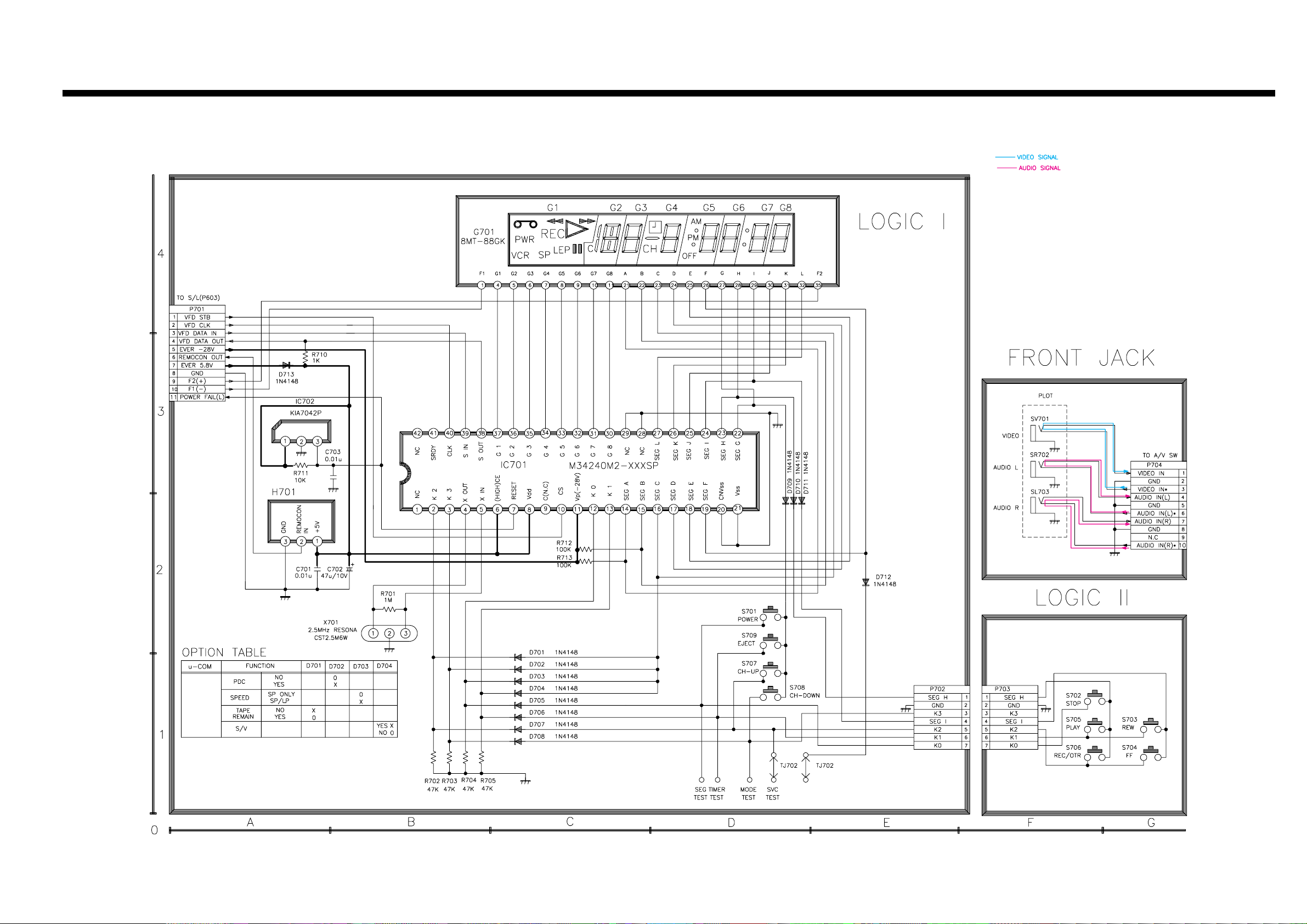
44
4-6. LOGIC CIRCUIT(DV -F882Series)
Page 48

45
4-7. HEAD-AMP CIRCUIT
Page 49

46
4-8. VIDEO CIRCUIT
Page 50

47
4-9. Hi-Fi AUDIO
Page 51

48
4-10. PIF NICAM MODULE
Page 52

49
4-11. PIF/MPX CIRCUIT(2 CARRIER)
Page 53

50
4-12. PIF CIRCUIT
Page 54

51
4-13. OSD CIRCUIT
Page 55

52
4-14. VPS/PDC CIRCUIT
Page 56

53
4-15. IN/OUT SW CIRCUIT I
Page 57

54
4-16. IN/OUT SW CIRCUIT II
Page 58

55
4-17. REMOCON CIRCUIT(DV -F882D)
Page 59

SECTION 5. VOLT AGE CHAR TS
V oltage Charts
1. IC151 (MC14053B)
PIN NO
MODE
REC PB REMARK
1 0 0 Conditions
2 0 0 : Line input
3 1.1 1.1 and PB mode
4 1.1 1.1
500
600
700
800
56
2. ICS01 (168K88E6ML)
PIN NO
MODE
REC PB REMARK
1 2.4 2.3 Conditions
2 2.3 2.3 : No signal
3 2.1 2.2
4 2.5 2.5
5 1.4 0.9
6 4.9 4.9
7 4.9 4.9
8 2.3 2.7
9 3.6 3.6
10 1.7 2.7
PIN N
MODE
REC PB REMARK
11 0 0
12 0 0
13 0 0
14 0 0
15 4.9 4.9
16 2.3 2.3
17 2.3 2.3
18 1 1.7
19 1 1.7
20 4.9 4.9
PIN NO
MODE
REC PB REMARK
9 2.3 2.3
10 0 0
11 2.3 2.3
12 0.7 0.7
13 1.1 1.1
14 1.1 1.1
15 0 0
16 2.3 2.3
Page 60
57
3. IC701 (M34240M2-XXXSP)
PIN NO
MODE
REC
10
20
30
4 2.8
5 2.4
65
75
85
90
10 0.5
11 -28
12 0
13 0
14 -17.2
15 -14.1
16 -17.1
17 -20
18 -17
19 -17
20 0
21 0
PIN NO
MODE
REC
22 -7.8
23 -20
24 -23
25 -23
26 -24
27 -24
28 0
29 0
30 -21
31 -21
32 -21
33 -21
34 -21
35 -21
36 -21
37 -21
38 0
39 0
40 5
41 0
42 0
Page 61

58
IC301 DC VOLTAGE (LA7437)
PIN NO
MODE
REC PB
1 3 2.2
2 3 2.8
344
4 2.5 2.1
5 3 2.7
6 4.4 2
7 4.8 2
8 4.8 4.8
9 2.4 2.8
10 1.8 1.5
11 3.1 3.1
12 4 2.8
13 4.8 4.8
14 0 4.2
15 3.1 4
16 1.5 1
17 5.2 0
18 2 2
19 0 0
20 1 1
21 2.2 0
PIN NO
MODE
REC PB
22 0 0
23 2.5 2.4
24 2.2 2.4
25 0 0
26 2 2.4
27 0 0
28 1.8 1.8
29 2.4 0
30 0 0
31 3.8 3.8
32 2.5 2.5
33 2 2
34 4.8 4.8
35 0 1.5
36 2.8 1.6
37 2.8 1.6
38 2 2.2
39 1.8 2
40 4.4 2
41 1.5 0.8
42 0 0
IC302 DC VOLTAGE (LA89970)
PIN NO
MODE
REC PB
100
2 2.5 2.4
355
4 2.5 2.4
500
6 2.5 2.2
700
8 1.4 1
900
10 2.4 0
11 0 1.4
PIN NO
MODE
REC PB
12 0 0
13 2 2
14 2 0
15 5 0
16 0 0
17 5 5
18 8.8 8.8
19 5 4.8
20 0 0
21 1.4 1.4
22 0 0
Page 62

59
ICS02 DC VOLTAGE (LVA519S)
ICS02 DC VOLTAGE (LVA519S)
PIN NO
MODE
REC PB
1 2.0 3.6
2 2.0 2.0
300
400
5 0.9 0.9
600
7 0 4.9
8 2.7 0
900
10 2.2 3.5
11 0 3.5
12 0 1.6
13 2.5 2.5
14 5 4.5
15 5 5
PIN NO
MODE
REC PB
16 0 1.6
17 0 4
18 0 0
19 2.0 3.6
20 0.7 0
21 0 4.0
22 2.0 3.6
23 0.7 0
24 0 4.0
25 0 0
26 0 0
27 0.7 0
28 2.2 3.6
29 0 0
30 0.7 0
PIN NO
MODE
REC PB
132
2 1.5 1.4
3 1.5 2
4 0.5 3.8
500
6 2.3 1.2
750
855
955
Page 63

60
IC201 (HI-FI AUDIO, TDA9614H)
PIN NO
MODE
REC PB
1 3.8 3.8
2 3.8 3.8
3 3.8 3.8
4 3.8 3.8
5 3.8 3.8
6 3.8 3.8
7 3.8 3.8
8 3.8 3.8
9 3.8 3.8
10 3.8 3.8
11 3.8 3.8
12 0 5
13 5 5
14 5 5
15 5 5
16 0 0
17 3.8 3.8
18 6 6
19 6 6
20 6 6
21 6 6
22 6 6
23 - 24 - 25 5.5 5.5
26 5.5 5.5
27
28 3.8 3.8
29 3.8 3.8
30 0 0
31 3.8 3.8
32 0 5
PIN NO
MODE
REC PB
33 6 6
34 3.8 3.8
35 3.8 3.8
36 3.8 3.8
37 3.8 3.8
38 3.8 3.8
39 3.8 3.8
40 3.8 3.8
41 2 42 3.8 3.8
43 0 0
44 2 45 3.8 3.8
46 3.8 3.8
47 3.8 3.8
48 3.8 3.8
49 3.8 3.8
50 12 12
51 3.8 3.8
52 3.3 3.8
53 3.8 3.8
54 0 0
55 0.6 0.6
56 1.2 1.2
57 1.9 1.9
58 5 5
59 3.8 3.8
60 0 0
61 PULSE PULSE
62 5 HI-FI: 5
NOR: 0
63 3.3 3.8
64 3.8 4.3
Page 64

61
ICB01 (AUDIO HEAD AMP, BA7743s)
AUDIO PART TR
PIN NO
MODE
REC PB
1 1.2 1.2
2 0.5 4.4
3 0.4 1.2
4 2.8 2.8
500
600
755
8 2 3.4
9 3 2.8
10 5 5
11 SP :0 SP :0
LP :5 LP :5
12 PULSE PULSE
PIN NO
MODE
REC PB
13 4.8 5
14 4 0
15 4 0
16 0 0.8
17 0 0.5
18 0 0
19 0 0.5
20 0 0.8
21 0 0
22 4 0
23 0.5 0
24 0.8 0
Tr NO
PORT
COLLECTOR BASE EMITTER
Q200 0 (0) 0 (1.5) 0 (0)
Q201 0 (0) 0 (1.5) 0 (0)
Q202 0 (0) 0 (1.5) 0 (0)
Q203 0 (1.5) 5 (0.5) 5
Q204 0 (0) 0.7 (0) 0 (0)
Q232 12 (0.5) 0 (0.5) 0 (0)
Q233 12 (0) 12 (12) 12 (12)
Q234 0 (12) 4.4 (0) 0 (0)
IC202 (NORMAL AUDIO SWITCHING, BA7755A)
PIN NO
MODE
REC PB
11212
200
300
4 4.4 0.5
599
Page 65

62
9. IC601 ( µ-COM)
NO NAME ASSIGNMENT ACTIVE
1 CTL/TEST CONTROL PULSE TEST PORT PULSE
2 VS/SHARP E.E. : VS TUNING, PULSE
PLAYBACK : SHARPNESS
3 CAP PWM CAPSTAN CONTROL PWM PULSE
OUTPUT
4 DRUM PWM DRUM CONTROL PWM PULSE
OUTPUT
5 S/REEL SUPLY REEL PULSE INPUT PULSE
6 T/REEL TAKE-UP REEL PULSE INPUT PULSE
7 MUTE 1 AUDIO/PIF MUTE 1 HIGH
8 DUAL DUAL HIGH
9 TAPE START TAPE START SENSOR LOW
DATA INPUT
10 N.C
11 REMOCON REMOCON DATA INPUT PORT PULSE
12 CAP. I. LIM CAPSTAN I.CONTROL LOW
13 CAP F/R CAPSTAN FWD/RVS L/H
14 PB (L) PLAY LOW LOW
15 C.ROTARY COLOR ROTARY PULSE
16 H.A/SWP HEAD AMP SWITCHING PULSE
17 ENVE/COMP ENVELOPE COMPARE PULSE
18 V.SWP VIDEO SWITCHING PULSE
19 Q-Vsync Q-Vsync PULSE/L
20 AUDIO SW AUDIO SWITCHING PULSE
21 TRICK/H TRICK/HIGH HIGH
22 REC (L) REC : LOW LOW
23 SP (H) SP : HIGH HIGH
24 LP (H) LP : HIGH HIGH
25 NICAM/A2 NICAM, A2
26 Vcc Vcc
27 A MUTE (2) AUDIO MUTE 2
28 POWER FAIL POWER FAIL PORT LOW
29 EE (L) E.E : LOW LOW
30 OSD STB OSD STROBE LOW
31 NTSC (H) NTSC : HIGH HIGH
32 LP TRICK LP TRICK HIGH
33 TV/VCR TV/VCR : PORT H/L
34 POWER/ON POWER ON/OFF CONTROL L/H
PORT
35 NUMA GND
36 NUMB GND
NO NAME ASSIGNMENT ACTIVE
37 RESET RESET INPUT PORT LOW
38 Xin 16MHZ OSC IN
39 Xout 16MHZ OSC OUT
40 CLK/SEL RESET : 32KHZ OSCILLATION LOW
41 Vss GND
42 Xcin 32.768KHZ OSC IN
43 Xcout 32.768KHz OSC OUT
44 TV/LINE TV/LINE : PORT H/L
45 LM/ON LOADING MOTOR ON HIGH
46 LM F/R LOADING MOTOR FWD/RVS L/H
47 CST/DOWN CASSETTE DOWN OUT LOW
48 REC SAFETY REC SAFETY SW DATA INPUT LOW
49 CAM A CAM A DATA INPUT LOW
50 CAM B CAM B DATA INPUT LOW
51 CAM C CAM C DATA INPUT LOW
52 CAM D CAM D DATA INPT LOW
53 VL BAND LOW : HIGH OUT HIGH
54 VH BAND HIGH : HIGH OUT HIGH
55 VU BAND UHF : HIGH OUT HIGH
56 AFT DEFEAT PAL TUNING : HIGH
AFT DEFEAT ON OUTPUT
57 STEREO STEREO: HIGH HIGH
58 VPS DATA VPS CONTROL : SERIAL DATA SERIAL
59 VPS CLK
VPS CONTROL : SERIAL CLOCK
SERIAL
60
EEPROM STB
EEPROM STORBE HIGH
61
EEPROM CLK
EEPROM SERIAL CLOCK SERIAL
62 EEPROM EEPROM SERIAL DATA SERIAL
DATA
63 A/V CLOCK A/V CONTROL SERIAL CLOCK SERIAL
64 A/V DATA A/V CONTROL SERIAL DATA SERIAL
65 AMP Vcc AMP Vcc
66 DRUM/PG DRUM PG INPUT PULSE
67 DRUM/FG DRUM FG INPUT PULSE
68 CAP/FG CAPSTAN FG INPUT PULSE
69 Vref OUT AMP REFERENCE Vcc
70 Vref In AMP REFERENCE Vcc
71 CLAMPF REFERENCE TO CTL CIRCUIT
72 CLAMPR REFERENCE TO CTL CIRCUIT
73 CTLAMPout REFERENCE TO CTL CIRCUIT
74 AMPC REFERENCE TO CTL CIRCUIT
75 CTLAMPin REFERENCE TO CTL CIRCUIT
76 CTL+SWout REFERENCE TO CTL CIRCUIT
Page 66

Tr NO.
PORTS
EMITTER
COLLECTOR
BASE
Q851 12.5 (12.6) 14.3 (14.1) 13.1 (13.1)
Q852 12.6 (12.7) 14.3 (14.1) 13.2 (13.3)
Q853 0 (0) 5.3 (0) 0 (5.2)
11. POWER PART TR
PORTS EMITTER COLLECTOR BASE
Tr NO. PB REC PB REC PB REC
QS02 2.46 1.47 4.89 4.89 3.1 2.1
Q302 2.8 1.68 0 0 2.1 0.97
Q303 1.948 2 4.95 4.97 2.56 2.67
Q305 4.96 4.96 4.97 4.88 4.23 5
Q311 3.46 2.42 0 0 2.74 1.7
10. VIDEO/OSD PART TR
Tr NO.
PORTS
EMITTER
COLLECTOR
BASE
Q854 0 (0) 0 (12.6) 5.4 (0)
Q855 12.6 (12.6) 12.6 (0.8) 11.9 (12.6)
Q856 5.0 (1.4) 5.9 (6.0) 5.7 (0.8)
Tr NO.
PORTS
EMITTER COLLECTOR BASE
Q604 4.9 (4.9) 4.9 (0.2) 4.3 (5)
Q603 1.0 (3.3) 0.1 (0) 0.4 (2.0)
12. SERVO PART TR
63
NO NAME ASSIGNMENT ACTIVE
76 CTL+SWout REFERENCE TO CTL CIRCUIT
77 CTL + REFERENCE TO CTL CIRCUIT
78 CTL- REFERENCE TO CTL CIRCUIT
79 GND GND
80 GND GND
81 Vcc Vcc
82
A/D Reference
REFERENCE Vcc
83 TAPE END TAPE END SENSOR LOW
DATA INPUT
84 CANAL + (L) CANAL : LOW INPUT LOW
85 PIF/ON VPS STANBY PIF ON HIGH
86 V.ENVE VIDEO DC ENVE A/D
87 RF AGC RF AGC
88 DRUM/SEL SYSTEM DRUM SELECT A/D
NO NAME ASSIGNMENT ACTIVE
89 BRKADJ SLOW BREAK ADJUST A/D
90 PGADJ PG DLAY ADJUST A/D
91 PATH PATH ADJUST A/D
92 AFT AFT INPUT PORT A/D
93 C.SYNC C.SYNC INPUT PORT PULSE
94 VFD DATA VFD SERIAL DATA OUT SERIAL
OUT
95 VFD DATA IN VFD SERIAL DATA IN SERIAL
96 VFD CLOCK VFD SERIAL CLOCK OUT SERIAL
97 VFD STB VFD STROBE LOW
98
OSD DATA OUT
OSD SERIAL DATA OUT SERIAL
99 N.C
100 OSD CLK OSD SERIAL CLOCK SERIAL
PLAY (PW OFF)
Page 67

69
SECTION 7. DIS ASSEMBLY
7-1. P ACKING AS (DV-F802Series)
No. Part Code Part Name Q'ty Description Re
1 97PB0935S- SET TOTAL AS 1
2 97P4803100 POLY BAG FOR SET 1 P.E FOAM
3 97P4920800 PAD LEFT/RIGHT 1 EPS
4 97P5040700 BOX CARTON 1
EX300 X SCP150 X E X 300
5 97P9531607 MANUAL OWNERS 1 ART PAPER
6 97P880RP15 CABLE RF 1 PAL 1.5M
7 47P7500001 BATTERY 2 AAM 1.5V
8 97P0424100 COVER ACCESSORY 1 LD-PE T0.1
9 97P1R2BC14
REMOCON HANDSET AS
1 VR-F2BT
Page 68

70
7-2. P ACKING AS (DV-F882Series)
No. Part Code Part Name Q'ty Description Re
1 97P4921200 PAD RIGHT/LEFT 1 EPS
2 97P4803100 POLY BAG FOR SET 1 P.E FOAM
3 97PB0959S SET TOTAL ASS'Y 1
4 97P5039900 BOX CARTON 1
EX300ƒNSCP150ƒNEX300
5 97P8804213 CABLE RF 1 PAL 1.5M
6 486A716200 BATTERY 2 AAA
7 97P0424100 COVER ACCESSORY 1 LE-PE T0.1
8 97P1R3BC13
REMOCON HANDSET AS
1 VR-F3BC
9 97P9560000 MANUSL OWNERS 1 ART PAPER (F882D)
Page 69

71
7-3. SET TOT AL AS (DV-F882 Series)
No. Part Code Part Name Q'ty Description Re
1 97P0608400 CHASSIS MAIN 1 ABS(HB)
2 97PD130800 PANEL FRONT AS 1
3 97PD132600 PCB LOGIC AS 1
4 97PD130300 PCB MAIN AS 1
5 97PB0588D- DECK TOTAL AS 1
6 97PB181500 PCB HEAD AMP AS 1
7 97PB208800 PCB A/V SW AS 1
8 97P0710710 BOARD ANT 1 HI-PS
9 97P0800600 LEG 2 SBR 80 BLK
10 97P0455710 COVER TOP 1 SECC T0.6+PVC T0.15
11 97P0455810 COVER BOTTOM 1 SECC T0.4
12 7173401211 SCREW TAPPTITE 3 TT2 BIN 4X12 MFZN
DEC
13 7173401211 SCREW TAPPTITE 2 TT2 BIN 4X12 MFZN
BOAR
14 7173401012 SCREW TAPTITE 5 TT2 BIN 4X10 BK MFZN
COVE
15 7174301011 SCREW TAPPTITE 3 TT2 RND 3X10 MFZN
C/BO
16 7173401211 SCREW TAPPTITE 2 TT2 BIN 4X12 MFZN
BRK
17 7274300811 SCREW TAPPTITE 1 TT2 BIN 4X12 MFZN
B/
18 7274300811 SCREW TAPPTITE 1 TT3 RND 3X6 MFZN
PREA
19 97P2440200 BRKT F/L 1 SECC T1.6
20 97P2441400 BRKT DECK 1 SECC T1.6
21 97P4213100 CUSHION F/L 2 EVA
22 97P4213500 CUSHION BRKT 1 EVA B
23 97P4213600 CUSHION B/D 1 EVA
Page 70

72
7-4. SET TOT AL AS (DV-F802 SERIES)
No. Part Code Part Name Q'ty Description Re
1 97P0608401 CHASSIS MAIN 1 HI-PS(HB)
2 97PC166300 PANEL FRONT AS 1
3 97PD106700 PCB LOGIC AS 1
4 97PD106600 PCB MAIN AS 1
5 97PB0666D- DECK TOTAL AS 1
6 97PB210300 PCB HEAD AMP AS 1
7 97PB210200 PCB A/V SW AS 1
8 97P0714100 BOARD ANT 1 HI-PS(HB)
9 97P0800600 LEG 2 SBR 80 BLK
10 97P0455710 COVER TOP 1 SECC T0.6+PVC T0.15
11 97P0455810 COVER BOTTOM 1 SECC T0.4
12 7173401211 SCREW TAPPTITE 3 TT2 BIN 4X12 MFZN
DEC
13 7173401411 SCREW TAPPTITE 2 TT2 BIN 4X12 MFZN
BOAR
14 7173401012 SCREW TAPTITE 5 TT2 BIN 4X10 BK MFZN
COVE
15 7174301011 SCREW TAPPTITE 3 TT2 RND 3X10 MFZN
C/BO
16 7173401211 SCREW TAPPTITE 2 TT2 BIN 4X12 MFZN
BRK
17 7174300611 SCREW TAPPTITE 1 TT2 BIN 4X12 MFZN B/
18 97P2440200 BRKT F/L 1 SECC T1.6
19 97P2441400 BRKT DECK 1 SECC T1.6
20 97P4213100 CUSHION F/L 2 EVA
21 97P4213500 CUSHION BRKT 1 EVA B
22 97P4213600 CUSHION B/D 1 EVA
Page 71

73
8-1. ST ANDARD PART NUMBER CODING
1. Fixed Resistor Coding
2. Semi-Fixed Resistor Coding
SECTION 8. ELECTRICAL P AR TS LIST
8-1-1. RESISTOR CODING
Type of Resistor
C Composition Resistor
D Carbon Resistor
F Fusible Resistor
K Ceramic Resistor
N Metal Film Resistor
S Metal-Oxide Film
Resistor
W Wire Wound Resistor
X Cement Resistor
Y Chip Resistor
Type of Resistor
Code Wattage
–A 1/6W
–8 1/8W
–4 1/4W
–2 1/2W
01 1W
02 2W
Distance
Code Distance
A 2.5 mm
B 5.0 mm
C 7.5 mm
D 10.0 mm
E 12.5 mm
F 15.0 mm
G 17.5 mm
H 20.0 mm
G 17.5 mm
H 20.0 mm
J 22.5 mm
K 25.0 mm
X Auto Insertion
Z Auto Insertion
Tolerance
Symbol
Tolerance
F ±1%
G ±2%
J ±5%
K ±10%
M ±20%
N ±30%
Value
Example
478..............0.47Ω
479................4.7Ω
470.................47Ω
471...............470Ω
472..............4.7KΩ
473 ..............47KΩ
Meterial Shape Knob Code
Pin Length Value
(Same as Fixed Type)
Knob
Type
VERTICAL
HORIZONTAL
VERTICAL
HORIZONTAL
VERTICAL
HORIZONTAL
CARBON
FILM
METAL
GRAZE
CARBON
SOLID
1
6
5
WITH 1 11
WITH 3 13
WITH 1 61
WITH 3 63
WITH 1 51
WITH 3 53
WITHOUT 2 12
WITHOUT 4 14
WITHOUT 2 62
WITHOUT 4 64
WITHOUT 2 52
WITHOUT 4 54
R
R
V
Page 72

74
1. Normal
2. Temperature Compensation
8-1-2. CAP ACITOR CODING
8-1-3. FUSE CODING
Type
F Fiber
G Glass Tube
L Lead Type
Glass Tube
T Temperature
W Wire
C Ceramic
P Plastic
Size
A MF41 4.6x16
B MF51 5.2x20
C MF60 6.3x30
D MF61 6.3x31.8
E MF01 10.3x38.1
F MF04 14.3x50.8
G MF05 20.5x76.2
Voltage
1 AC125V
2 AC250V
3 125/250V
Type
Code Type
A Aluminum
B Barrier Layer
C Ceramic
E Electrolytic
L Line Across
M Mylar
S Styrol
N Metalized Polyester
Q Mica
Oil
T Tantal
Voltage
Code Voltage
0J 6.3V
1A 10V
1C 16V
1D 20V
1E 25V
1V 35V
1G 40V
1H 50V
1J 63V
2A 100V
2B 125V
2C 160V
2D 200V
2E 250V
2F 315V
Characteristic
Capacitance Temperature
Coefficient (ppm/˚C) Coefficient (ppm/˚C)
A +100 F ±15
B +30 G ±30
C0 H ±60
H –30 J ±120
L –80 K ±250
P –150 L ±500
R –220 M ±1000
S –330 N ±2500
T –470
U –750
V –1000
SI +350~
–1000
Distance
(Same As
Fixed
Resistor)
Value
(Same as Fixed
Resistor)
Shape
or
Characteristic
Tolerance
(Same as Fixed
Resistor)
Distance
(Same as Fixed
Resistor)
Voltage
(Same as Normal)
Value
(Same as Fixed Resistor)
Tolerance
(Same as Fixed Resistor)
Regulation Value
(Same as Fixed Resistor)
Characteristics
Page 73

8-2. ELECTRICAL P AR TS LIST
PCB MAIN AS
75
REF. PART CODE PART NAME PART DESCRIPTION
CS01 HCLK240JCA C CHIP CERA 50V SL 24PF J 2012
CS02 HCLK240JCA C CHIP CERA 50V SL 24PF J 2012
CS03 HCLK121JCA C CHIP CERA 50V SL 120PF J 2012
CS04 HCFK103ZCA C CHIP CERA 50V Y5V 0.01MF Z 2012
CS05 CEXF1H228V C ELECTRO 50V RSS 0.22MF (5X11) TP
CS06 HCQK180JCA C CHIP CERA 50V CH 18PF J 2012
CS07 HCQK180JCA C CHIP CERA 50V CH 18PF J 2012
CS08 CEXF1C470A C ELECTRO 16V RSM 47MF (6.3X7) TP
CS11 HCFK103ZCA C CHIP CERA 50V Y5V 0.01MF Z 2012
CS12 CEXF1H100V C ELECTRO 50V RSS 10MF (5X11) TP
CS14 HCLK560JCA C CHIP CERA 50V SL 56PF J 2012
CS15 HCFK104ZCA C CHIP CERA 50V Y5V 0.1MF Z 2012
CS16 CEXF1H109V C ELECTRO 50V RSS 1MF (5X11) TP
CS17 CMXM2A223J C MYLAR 100V 0.022MF J TP
CS18 CMXM2A332J C MYLAR 100V 3300PF J TP
CS19 CZXC1H561J C CERA MONOLITHIC 50V NPO 560PF J
CS20 HCFK103ZCA C CHIP CERA 50V Y5V 0.01MF Z 2012
CS21 HCLK201JCA C CHIP CERA 50V SL 200PF J 2012
CS22 HCLK201JCA C CHIP CERA 50V SL 200PF J 2012
CS23 HCLK201JCA C CHIP CERA 50V SL 200PF J 2012
CS24 CEXF1E220V C ELECTRO 25V RSS 22MF 5X11
C111 CEXF1H100A C ELECTRO 50V RSM 10MF 6.3X7
C171 HCFK103ZCA C CHIP CERA 50V Y5V 0.01MF Z 2012
C172 CEXF1E470V C ELECTRO 25V RSS 47MF (5X11) TP
C173 CEXF1H228V C ELECTRO 50V RSS 0.22MF (5X11) TP
C174 HCFK103ZCA C CHIP CERA 50V Y5V 0.01MF Z 2012
C175 HCFK103ZCA C CHIP CERA 50V Y5V 0.01MF Z 2012
C176 HCFK103ZCA C CHIP CERA 50V Y5V 0.01MF Z 2012
C177 CEXF1H478V C ELECTRO 50V RSS 0.47MF (5X11) TP
C178 HCFK103ZCA C CHIP CERA 50V Y5V 0.01MF Z 2012
C179 CEXF1E470V C ELECTRO 25V RSS 47MF (5X11) TP
C182 HCFK103ZCA C CHIP CERA 50V Y5V 0.01MF Z 2012
C183 CMXM2A104J C MYLAR 100V 0.1MF J TP
C184 CMXM2A104J C MYLAR 100V 0.1MF J TP
C185 CMXM2A104J C MYLAR 100V 0.1MF J TP
C186 HCQK131JCA C CHIP CERA 50V CH 130PF J 2012
C188 HCFK103ZCA C CHIP CERA 50V Y5V 0.01MF Z 2012
C189 CEXF1E470V C ELECTRO 25V RSS 47MF (5X11) TP
C190 HCFK103ZCA C CHIP CERA 50V Y5V 0.01MF Z 2012
REF. PART CODE PART NAME PART DESCRIPTION
C191 CEXF1E470V C ELECTRO 25V RSS 47MF (5X11) TP
C192 CEXF1C101V C ELECTRO 16V RSS 100MF (6.3X11) TP
C193 CEXF1H109V C ELECTRO 50V RSS 1MF (5X11) TP
C194 CEXF1H109V C ELECTRO 50V RSS 1MF (5X11) TP
C195 HCFK104ZCA C CHIP CERA 50V Y5V 0.1MF Z 2012
C234 CMXM2A473J C MYLAR 100V 0.047MF J TP
C241 CEXF1H109A C ELECTRO 50V RSM 1MF (4X7) TP
C242 CEXF1H109A C ELECTRO 50V RSM 1MF (4X7) TP
C243 CEXF1C479A C ELECTRO 16V RSM 4.7MF 4*7
C301 HCLK680JCA C CHIP CERA 50V SL 68PF J 2012
C302 CEXF1H109A C ELECTRO 50V RSM 1MF (4X7) TP
C304 HCLK201JCA C CHIP CERA 50V SL 200PF J 2012
C305 HCQK150JCA C CHIP CERA 50V CH 15PF J 2012
C306 HCLK161JCA C CHIP CERA 50V SL 160PF J 2012
C307 HCLK430JCA C CHIP CERA 50V SL 43PF J 2012
C308 HCLK201JCA C CHIP CERA 50V SL 200PF J 2012
C309 HCLK360JCA C CHIP CERA 50V SL 36PF J 2012
C310 HCFK103ZCA C CHIP CERA 50V Y5V 0.01MF Z 2012
C311 CBZP1C103M C CERA SEMI 16V Y5S 0.01MF M (AXIAL)
C312 HCLK391JCA C CHIP CERA 50V SL 390PF J 2012
C314 CEXF1H479V C ELECTRO 50V RSS 4.7MF (5*11) TP
C315 HCFK223ZCA C CHIP CERA 50V Y5V 0.022MF Z 2012
C317 HCFK103ZCA C CHIP CERA 50V Y5V 0.01MF Z 2012
C318 CEXF1C470A C ELECTRO 16V RSM 47MF (6.3X7) TP
C319 CEXF1H100V C ELECTRO 50V RSS 10MF (5X11) TP
C320 HCFK103ZCA C CHIP CERA 50V Y5V 0.01MF Z 2012
C321 CEXF1C470A C ELECTRO 16V RSM 47MF (6.3X7) TP
C322 CEXF1H109A C ELECTRO 50V RSM 1MF (4X7) TP
C323 CEXF1H109A C ELECTRO 50V RSM 1MF (4X7) TP
C324 HCFK103ZCA C CHIP CERA 50V Y5V 0.01MF Z 2012
C325 HCFK223ZCA C CHIP CERA 50V Y5V 0.022MF Z 2012
C326 CEXF1C470A C ELECTRO 16V RSM 47MF (6.3X7) TP
C327 HCFK103ZCA C CHIP CERA 50V Y5V 0.01MF Z 2012
C328 CEXF1C470A C ELECTRO 16V RSM 47MF (6.3X7) TP
C329 HCFK104ZCA C CHIP CERA 50V Y5V 0.1MF Z 2012
C330 CEXF1C470A C ELECTRO 16V RSM 47MF (6.3X7) TP
C331 HCFK103ZCA C CHIP CERA 50V Y5V 0.01MF Z 2012
C332 CEXF1H109A C ELECTRO 50V RSM 1MF (4X7) TP
C336 HCFK103ZCA C CHIP CERA 50V Y5V 0.01MF Z 2012
Page 74

76
REF. PART CODE PART NAME PART DESCRIPTION
C337 HCFK103ZCA C CHIP CERA 50V Y5V 0.01MF Z 2012
C338 HCFK103ZCA C CHIP CERA 50V Y5V 0.01MF Z 2012
C339 HCLK121JCA C CHIP CERA 50V SL 120PF J 2012
C340 CEXF1H108A C ELECTRO 50V RSM 0.1MF 4X7
C343 CMXM2A223J C MYLAR 100V 0.022MF J TP
C344 HCFK473ZCA C CHIP CERA 50V Y5V 0.047MF Z 2012
C345 CEXF1H109A C ELECTRO 50V RSM 1MF (4X7) TP
C346 CEXF1C470A C ELECTRO 16V RSM 47MF (6.3X7) TP
C347 HCFK103ZCA C CHIP CERA 50V Y5V 0.01MF Z 2012
C348 CEXF1H109A C ELECTRO 50V RSM 1MF (4X7) TP
C349 CMXM2A223J C MYLAR 100V 0.022MF J TP
C350 CEXF1H109A C ELECTRO 50V RSM 1MF (4X7) TP
C351 CMXM2A473J C MYLAR 100V 0.047MF J TP
C352 HCFK473ZCA C CHIP CERA 50V Y5V 0.047MF Z 2012
C353 CBZP1C103M C CERA SEMI 16V Y5S 0.01MF M (AXIAL)
C354 CEXF1C470A C ELECTRO 16V RSM 47MF (6.3X7) TP
C357 CEXF1C470A C ELECTRO 16V RSM 47MF (6.3X7) TP
C358 HCFK223ZCA C CHIP CERA 50V Y5V 0.022MF Z 2012
C362 CEXF1C470A C ELECTRO 16V RSM 47MF (6.3X7) TP
C363 HCFK103ZCA C CHIP CERA 50V Y5V 0.01MF Z 2012
C501 HCFK103ZCA C CHIP CERA 50V Y5V 0.01MF Z 2012
C502 HCBK102KCA C CHIP CERA 50V X7R 1000PF K 2012
C504 CEXF1H100A C ELECTRO 50V RSM 10MF 6.3X7
C505 CEXF1H100A C ELECTRO 50V RSM 10MF 6.3X7
C506 CEXF1C470A C ELECTRO 16V RSM 47MF (6.3X7) TP
C507 CEXF1H100A C ELECTRO 50V RSM 10MF 6.3X7
C508 CEXF1H109A C ELECTRO 50V RSM 1MF (4X7) TP
C509 CEXF1H109A C ELECTRO 50V RSM 1MF (4X7) TP
C510 HCFK104ZCA C CHIP CERA 50V Y5V 0.1MF Z 2012
C511 HCBK102KCA C CHIP CERA 50V X7R 1000PF K 2012
C512 HCBK102KCA C CHIP CERA 50V X7R 1000PF K 2012
C513 CMXM2A223J C MYLAR 100V 0.022MF J TP
C514 CMXM2A223J C MYLAR 100V 0.022MF J TP
C515 HCFK103ZCA C CHIP CERA 50V Y5V 0.01MF Z 2012
C516 HCFK103ZCA C CHIP CERA 50V Y5V 0.01MF Z 2012
C517 HCFK103ZCA C CHIP CERA 50V Y5V 0.01MF Z 2012
C518 CEXF1A471V C ELECTRO 10V RSS 470MF 8X11.5
C551 HCFK104ZCA C CHIP CERA 50V Y5V 0.1MF Z 2012
C601 CEXF1C470A C ELECTRO 16V RSM 47MF (6.3X7) TP
C602 CEXF1C470A C ELECTRO 16V RSM 47MF (6.3X7) TP
C603 CEXF1C470A C ELECTRO 16V RSM 47MF (6.3X7) TP
C605 CEXF1C470A C ELECTRO 16V RSM 47MF (6.3X7) TP
REF. PART CODE PART NAME PART DESCRIPTION
C606 HCQK180JCA C CHIP CERA 50V CH 18PF J 2012
C607 HCQK180JCA C CHIP CERA 50V CH 18PF J 2012
C608 HCQK220JCA C CHIP CERA 50V CH 22PF J 2012
C609 HCQK220JCA C CHIP CERA 50V CH 22PF J 2012
C610 HCFK103ZCA C CHIP CERA 50V Y5V 0.01MF Z 2012
C611 CEXF1A471V C ELECTRO 10V RSS 470MF 8X11.5
C616 HCLK101JCA C CHIP CERA 50V SL 100PF J 2012
C617 HCLK101JCA C CHIP CERA 50V SL 100PF J 2012
C618 HCLK101JCA C CHIP CERA 50V SL 100PF J 2012
C619 CEXF1E470V C ELECTRO 25V RSS 47MF (5X11) TP
C620 HCFK103ZCA C CHIP CERA 50V Y5V 0.01MF Z 2012
C621 CMXM2A103J C MYLAR 100V 0.01MF J (TP)
C622 CMXM2A103J C MYLAR 100V 0.01MF J (TP)
C623 CDXA0H104K C SUPER 5.5V 0.1F TAPING
C630 CEXF1C470A C ELECTRO 16V RSM 47MF (6.3X7) TP
C631 HCFK104ZCA C CHIP CERA 50V Y5V 0.1MF Z 2012
C633 HCFK104ZCA C CHIP CERA 50V Y5V 0.1MF Z 2012
C634 HCFK104ZCA C CHIP CERA 50V Y5V 0.1MF Z 2012
C635 HCFK103ZCA C CHIP CERA 50V Y5V 0.01MF Z 2012
C660 HCFK104ZCA C CHIP CERA 50V Y5V 0.1MF Z 2012
C661 HCFK104ZCA C CHIP CERA 50V Y5V 0.1MF Z 2012
C663 CBZP1C103M C CERA SEMI 16V Y5S 0.01MF M (AXIAL)
C664 HCFK103ZCA C CHIP CERA 50V Y5V 0.01MF Z 2012
C665 HCFK103ZCA C CHIP CERA 50V Y5V 0.01MF Z 2012
C667 HCLK101JCA C CHIP CERA 50V SL 100PF J 2012
C673 HCFK103ZCA C CHIP CERA 50V Y5V 0.01MF Z 2012
C674 HCLK101JCA C CHIP CERA 50V SL 100PF J 2012
C801 CL1UE3104M C LINE ACROSS 275V AC 1.40 SERIES U/C/V
C802 CH1HEB101M C CERA AC AC250V 100PF M U/C/V/S/N/
C803 CH1HEB101M C CERA AC AC250V 100PF M U/C/V/S/N/
C804 CH1FEE472M C CERA AC AC250V 4700PF M U/C/V KH
C807 CEXN2G820P C ELECTRO 400V LHS 82MF
C810 CEXF1H470V C ELECTRO 50V RSS 47MF (6.3*11) TP
C817 CEXF1E102F C ELECTRO 25V RX 1000MF 13X25
C818 CEXF1E331F C ELECTRO 25V RX 330MF 10X20
C825 CEXF1A102F C ELECTRO 10V RX 1000MF 10X20
C832 CCXF1H103Z C CERA 50V F 0.01MF Z (TAPPING)
C851 CEXF1H470V C ELECTRO 50V RSS 47MF (6.3*11) TP
C852 CEXF1E470V C ELECTRO 25V RSS 47MF (5X11) TP
C854 CEXF1E470V C ELECTRO 25V RSS 47MF (5X11) TP
C855 CEXF1E470V C ELECTRO 25V RSS 47MF (5X11) TP
C856 CEXF1E470V C ELECTRO 25V RSS 47MF (5X11) TP
Page 75

77
REF. PART CODE PART NAME PART DESCRIPTION
C857 CEXF1E470V C ELECTRO 25V RSS 47MF (5X11) TP
C858 CEXF1C470A C ELECTRO 16V RSM 47MF (6.3X7) TP
C859 CEXF1C470A C ELECTRO 16V RSM 47MF (6.3X7) TP
D301 DZN4148--- DIODE 1N4148 AUTO 52MM
D302 DZN4148--- DIODE 1N4148 AUTO 52MM
D303 DZN4148--- DIODE 1N4148 AUTO 52MM
D304 DZN4148--- DIODE 1N4148 AUTO 52MM
D305 DZN4148--- DIODE 1N4148 AUTO 52MM
D306 DZN4148--- DIODE 1N4148 AUTO 52MM
D307 DZN4148--- DIODE 1N4148 AUTO 52MM
D310 DZN4148--- DIODE 1N4148 AUTO 52MM
D601 DZN4148--- DIODE 1N4148 AUTO 52MM
D602 DZN4003--- DIODE IN4003
D603 DZN4003--- DIODE IN4003
D604 DZN4003--- DIODE IN4003
D605 DZZ3R9B--- DIODE ZENER DZ 3R9B (3R9) (AUTO)
D606 DS1R481T-- LED IR SIR-48IT
D606A 97P2334200 HOLDER LED SENSORPOM
D607 DZZ7R5BM-- DIODE ZENER UZ-7.5BM
D608 DZA105R1L- DIODE ZENER MA 1051L (5R1)
D609 DZN4003--- DIODE IN4003
D650 DZZ3R9B--- DIODE ZENER DZ 3R9B (3R9) (AUTO)
D801 DS1WBA60-- DIODE BRIDGE S1WBA60
D820 DZZP33BM-- DIODE ZENER UZP-33B 1W
D851 1KA33V---- IC ZENER KA33V
D852 DZZ13BL--- DIODE ZENER UZ-13BL
D853 DZZ13BL--- DIODE ZENER UZ-13BL
D854 DZN4003--- DIODE IN4003
D855 DZZ5R6BM-- DIODE ZENER DZ 5.6BM (AUTO)
D857 DZN4148--- DIODE 1N4148 AUTO 52MM
F01A 97P2316600 HOLDER AC CORD NYLON66 UL/CSA
F801A 97P460170P CLIP FUSE PFC5000-0702
F801B 97P460170P CLIP FUSE PFC5000-0702
ICS01 168K88E6ML IC OSD M35013-053SP (88E6ML)
ICS02 1LVA519S-- IC LVA519S (SYNC.SEPARATOR)
IC301 1LA7437--- IC VIDEO (PAL) LA7437
IC302 1LC89970-- IC VIDEO LC89970 PAL CCD
IC601 168KF8U8TS IC MICOM M37774M5H-519GP (F8U8TS)
IC602 1BA6209--- IC BA6209
IC603 14JN93C66- IC EEPROM AT93C66
IC604 1MN1380L--
IC COMPARATOR(RESET)
MN1380-L(RESET IC)
JPT01 85801065GY WIRE COPPER AWG22 1/0.65 TIN COATING
REF. PART CODE PART NAME PART DESCRIPTION
JPT02 85801065GY WIRE COPPER AWG22 1/0.65 TIN COATING
JPT03 85801065GY WIRE COPPER AWG22 1/0.65 TIN COATING
LS01 5CPX101J-- COIL PEAKING PL 100UH J (TAPPING)
LS02 5CPX150J-- COIL PEAKING 15UH J RADIAL
LS03 5CPX100J-- COIL PEAKING PL 10UH J (TAPPING)
L171 5CPX101J-- COIL PEAKING PL 100UH J (TAPPING)
L172 HLM100K01B L CHIP MULTI 10UH MLF3216C100KT
L173 5CPX100J-- COIL PEAKING PL 10UH J (TAPPING)
L301 5CPX330J-- COIL PEAKING 33UH J RADIAL
L302 5CPX330J-- COIL PEAKING 33UH J RADIAL
L303 5CPX271J-- COIL PEAKING 270UH J RADIAL
L304 5CPX820J-- COIL PEAKING 82UH J RADIAL
L305 5CPX100J-- COIL PEAKING PL 10UH J (TAPPING)
L306 5CPX100J-- COIL PEAKING PL 10UH J (TAPPING)
L309 5CPX330J-- COIL PEAKING 33UH J RADIAL
L310 5CPX100J-- COIL PEAKING PL 10UH J (TAPPING)
L312 5CPX100J-- COIL PEAKING PL 10UH J (TAPPING)
L801 5PLFSQ2014 FILTER LINE SQ-2014 40MH
L802 5PLFSQ2014 FILTER LINE SQ-2014 40MH
L803 56C220K686 COIL CHOKE 22UH K 27.5X0.4D
L804 56C220K686 COIL CHOKE 22UH K 27.5X0.4D
M801 97PB216300
AUTO VOLT REGULATOR
DV-F542DY-RF/D
PL101 97P62T02BF CONN B/B TUC-PP PLUG 2.0MM 15P
PL102 97P62T02BA CONN B/B TUC-PP PLUG 2.0MM 10P
PT01 97P6269000 CONN WAFER 00-8283-0612-00000
P101 97P62G02BL CONN B/B GB200 PLUG 2.0MM 20P
P106 97P62G02B5 CONN B/B GB200 PLUG 2.0MM 5P
P107 97P62G02BH CONN B/B GB200 PLUG 2.0MM 17P
P201 97P8851210 CONN AS (Y51210) 2H-2S 100MM
P501 97P6291736 CONN WAFER TKC-M08P-B1
P601 97P6291741 CONN WAFER TKC-M18P-B1
P603 97P8810B14 CONN AS (Y10B14) 11H-11S 140MM
P801 97P62Y02X2 CONN WAFER YFW800 STR 10MM 2P
QS02 TZTA1266Y- TR KTA1266Y- (AUTO)(1015Y)
Q171 TZSR1001-- TR KSR1001 (AUTO)
Q172 TZTA1273Y- TR KTA1273Y(966Y)
Q173 TZSR1001-- TR KSR1001 (AUTO)
Q174 TZSR1001-- TR KSR1001 (AUTO)
Q175 TZSR1001-- TR KSR1001 (AUTO)
Q176 TZSR2004-- TR KSR 2004 (TAPPING)
Q177 TZSR2004-- TR KSR 2004 (TAPPING)
Page 76

78
REF. PART CODE PART NAME PART DESCRIPTION
Q179 TZTK30AGR- FET KTK30A-GR (AUTO)
Q183 TZSR1001-- TR KSR1001 (AUTO)
Q184 TZTC3198Y- TR KTC3198Y-(1815Y) (AUTO)
Q187 TZSR1001-- TR KSR1001 (AUTO)
Q188 TZTA1273Y- TR KTA1273Y(966Y)
Q200 TZTC3203Y- TR KTC3203Y (2120Y)
Q201 TZTC3203Y- TR KTC3203Y (2120Y)
Q202 TZTC3203Y- TR KTC3203Y (2120Y)
Q203 TZTA1266Y- TR KTA1266Y- (AUTO)(1015Y)
Q205 TZTA1266Y- TR KTA1266Y- (AUTO)(1015Y)
Q302 TZTC3198Y- TR KTC3198Y-(1815Y) (AUTO)
Q303 TZTA1266Y- TR KTA1266Y- (AUTO)(1015Y)
Q305 TZTC3198Y- TR KTC3198Y-(1815Y) (AUTO)
Q311 TZTA1266Y- TR KTA1266Y- (AUTO)(1015Y)
Q603 TZTA1266Y- TR KTA1266Y- (AUTO)(1015Y)
Q604 TZTA1266Y- TR KTA1266Y- (AUTO)(1015Y)
Q851 TZTC3205Y- TR KTC3205Y (2236Y)
Q852 TZTC3205Y- TR KTC3205Y (2236Y)
Q853 TZSR1004-- TR KSR1004 (AUTO)
Q854 TZSR1004-- TR KSR1004 (AUTO)
Q855 TZTA1273Y- TR KTA1273Y(966Y)
Q856 TZTC3205Y- TR KTC3205Y (2236Y)
RS01 RD-2Z391J- R CARBON FILM 1/2 390 OHM J
RS02 HRFT753JCA R CHIP 1/10 75K OHM J 2012
RS03 HRFT472JCA R CHIP 1/10 4.7K OHM J 2012
RS10 RD-AZ562J- R CARBON FILM 1/6 5.6K OHM J
RS11 HRFT205JCA R CHIP 1/10 2M OHM J 2012
RS12 HRFT123FCA R CHIP 1/10 12K OHM F 2012
RS13 HRFT273JCA R CHIP 1/10 27K OHM J 2012
RS14 HRFT272JCA R CHIP 1/10 2.7K OHM J 2012
RS15 HRFT222JCA R CHIP 1/10 2.2K OHM J 2012
RS16 HRFT222JCA R CHIP 1/10 2.2K OHM J 2012
RS20 HRFT561JCA R CHIP 1/10 560 OHM J 2012
R121 HRFT102JCA R CHIP 1/10 1K OHM J 2012
R122 HRFT103JCA R CHIP 1/10 10K OHM J 2012
R124 HRFT183JCA R CHIP 1/10 18K OHM J 2012
R170 HRFT114JCA R CHIP 1/10 110K OHM J 2012
R171 HRFT433JCA R CHIP 1/10 43K OHM J 2012
R172 HRFT333JCA R CHIP 1/10 33K OHM J 2012
R173 RD-AZ183J- R CARBON FILM 1/6 18K OHM J
R174 HRFT222JCA R CHIP 1/10 2.2K OHM J 2012
REF. PART CODE PART NAME PART DESCRIPTION
R176 HRFT103JCA R CHIP 1/10 10K OHM J 2012
R178 HRFT105JCA R CHIP 1/10 1M OHM J 2012
R179 HRFT272JCA R CHIP 1/10 2.7K OHM J 2012
R182 HRFT103JCA R CHIP 1/10 10K OHM J 2012
R183 HRFT752JCA R CHIP 1/10 7.5K OHM J 2012
R184 HRFT103JCA R CHIP 1/10 10K OHM J 2012
R185 HRFT303JCA R CHIP 1/10 30K OHM J 2012
R186 HRFT103JCA R CHIP 1/10 10K OHM J 2012
R188 HRFT122JCA R CHIP 1/10 1.2K OHM J 2012
R190 RV5426103E R SEMI FIXED H10K-5X3-6Y-PC-GS
R191 HRFT103JCA R CHIP 1/10 10K OHM J 2012
R195 HRFT202JCA R CHIP 1/10 2K OHM J 2012
R198 HRFT564JCA R CHIP 1/10 560K OHM J 2012
R199 HRFT334JCA R CHIP 1/10 330K OHM J 2012
R200 RD-AZ102J- R CARBON FILM 1/6 1K OHM J
R221 HRFT102JCA R CHIP 1/10 1K OHM J 2012
R222 HRFT102JCA R CHIP 1/10 1K OHM J 2012
R223 RD-AZ472J- R CARBON FILM 1/6 4.7K OHM J
R224 RD-AZ102J- R CARBON FILM 1/6 1K OHM J
R225 HRFT333JCA R CHIP 1/10 33K OHM J 2012
R241 HRFT104JCA R CHIP 1/10 100K OHM J 2012
R242 HRFT104JCA R CHIP 1/10 100K OHM J 2012
R243 RD-AZ152J- R CARBON FILM 1/6 1.5K OHM J
R244 HRFT102JCA R CHIP 1/10 1K OHM J 2012
R301 HRFT202JCA R CHIP 1/10 2K OHM J 2012
R302 HRFT181JCA R CHIP 1/10 180 OHM J 2012
R303 HRFT681JCA R CHIP 1/10 680 OHM J 2012
R304 HRFT511JCA R CHIP 1/10 510 OHM J 2012
R305 HRFT473JCA R CHIP 1/10 47K OHM J 2012
R307 HRFT471JCA R CHIP 1/10 470 OHM J 2012
R308 HRFT221JCA R CHIP 1/10 220 OHM J 2012
R309 HRFT132JCA R CHIP 1/10 1.3K OHM J 2012
R310 HRFT472JCA R CHIP 1/10 4.7K OHM J 2012
R312 HRFT472JCA R CHIP 1/10 4.7K OHM J 2012
R313 HRFT102JCA R CHIP 1/10 1K OHM J 2012
R316 HRFT272JCA R CHIP 1/10 2.7K OHM J 2012
R317 HRFT681JCA R CHIP 1/10 680 OHM J 2012
R319 RD-AZ563J- R CARBON FILM 1/6 56K OHM J
R320 HRFT103JCA R CHIP 1/10 10K OHM J 2012
R322 RD-AZ101J- R CARBON FILM 1/6 100 OHM J
R324 RD-AZ102J- R CARBON FILM 1/6 1K OHM J
Page 77

79
REF. PART CODE PART NAME PART DESCRIPTION
R327 HRFT102JCA R CHIP 1/10 1K OHM J 2012
R328 HRFT103JCA R CHIP 1/10 10K OHM J 2012
R330 HRFT103JCA R CHIP 1/10 10K OHM J 2012
R331 HRFT103JCA R CHIP 1/10 10K OHM J 2012
R333 HRFT681JCA R CHIP 1/10 680 OHM J 2012
R334 HRFT222JCA R CHIP 1/10 2.2K OHM J 2012
R336 HRFT822JCA R CHIP 1/10 8.2K OHM J 2012
R337 HRFT102JCA R CHIP 1/10 1K OHM J 2012
R340 RD-AZ472J- R CARBON FILM 1/6 4.7K OHM J
R341 HRFT472JCA R CHIP 1/10 4.7K OHM J 2012
R355 HRFT182JCA R CHIP 1/10 1.8K OHM J 2012
R356 HRFT101JCA R CHIP 1/10 100 OHM J 2012
R390 HRFT103JCA R CHIP 1/10 10K OHM J 2012
R391 HRFT103JCA R CHIP 1/10 10K OHM J 2012
R501 HRFT332JCA R CHIP 1/10 3.3K OHM J 2012
R502 HRFT221JCA R CHIP 1/10 220 OHM J 2012
R504 RD-AZ103J- R CARBON FILM 1/6 10K OHM J
R505 HRFT273JCA R CHIP 1/10 27K OHM J 2012
R506 RD-AZ103J- R CARBON FILM 1/6 10K OHM J
R507 HRFT472JCA R CHIP 1/10 4.7K OHM J 2012
R508 RD-AZ182J- R CARBON FILM 1/6 1.8K OHM J
R509 HRFT182JCA R CHIP 1/10 1.8K OHM J 2012
R510 HRFT103JCA R CHIP 1/10 10K OHM J 2012
R511 HRFT332JCA R CHIP 1/10 3.3K OHM J 2012
R512 HRFT153JCA R CHIP 1/10 15K OHM J 2012
R513 HRFT103JCA R CHIP 1/10 10K OHM J 2012
R514 HRFT473JCA R CHIP 1/10 47K OHM J 2012
R515 HRFT103JCA R CHIP 1/10 10K OHM J 2012
R516 HRFT473JCA R CHIP 1/10 47K OHM J 2012
R517 HRFT103JCA R CHIP 1/10 10K OHM J 2012
R518 HRFT474JCA R CHIP 1/10 470K OHM J 2012
R519 HRFT273JCA R CHIP 1/10 27K OHM J 2012
R520 RD-AZ103J- R CARBON FILM 1/6 10K OHM J
R521 RD-AZ103J- R CARBON FILM 1/6 10K OHM J
R522 RD-AZ103J- R CARBON FILM 1/6 10K OHM J
R601 HRFT103JCA R CHIP 1/10 10K OHM J 2012
R602 HRFT103JCA R CHIP 1/10 10K OHM J 2012
R603 HRFT103JCA R CHIP 1/10 10K OHM J 2012
R604 RD-AZ103J- R CARBON FILM 1/6 10K OHM J
R605 HRFT152JCA R CHIP 1/10 1.5K OHM J 2012
R606 HRFT154JCA R CHIP 1/10 150K OHM J 2012
R607 RD-AZ471J- R CARBON FILM 1/6 470 OHM J
R608 RD-AZ471J- R CARBON FILM 1/6 470 OHM J
REF. PART CODE PART NAME PART DESCRIPTION
R609 RD-AZ471J- R CARBON FILM 1/6 470 OHM J
R610 RD-AZ471J- R CARBON FILM 1/6 470 OHM J
R611 HRFT103JCA R CHIP 1/10 10K OHM J 2012
R612 HRFT103JCA R CHIP 1/10 10K OHM J 2012
R613 HRFT103JCA R CHIP 1/10 10K OHM J 2012
R614 HRFT103JCA R CHIP 1/10 10K OHM J 2012
R615 HRFT153JCA R CHIP 1/10 15K OHM J 2012
R616 HRFT153JCA R CHIP 1/10 15K OHM J 2012
R617 HRFT102JCA R CHIP 1/10 1K OHM J 2012
R618 HRFT153JCA R CHIP 1/10 15K OHM J 2012
R619 HRFT302JCA R CHIP 1/10 3K OHM J 2012
R620 HRFT103JCA R CHIP 1/10 10K OHM J 2012
R621 HRFT472JCA R CHIP 1/10 4.7K OHM J 2012
R622 HRFT472JCA R CHIP 1/10 4.7K OHM J 2012
R623 HRFT104JCA R CHIP 1/10 100K OHM J 2012
R624 RD-4Z106J- R CARBON FILM 1/4 10M OHM J
R625 HRFT105JCA R CHIP 1/10 1M OHM J 2012
R626 HRFT511JCA R CHIP 1/10 510 OHM J 2012
R628 HRFT154JCA R CHIP 1/10 150K OHM J 2012
R629 RD-AZ102J- R CARBON FILM 1/6 1K OHM J
R631 RD-AZ102J- R CARBON FILM 1/6 1K OHM J
R633 HRFT102JCA R CHIP 1/10 1K OHM J 2012
R634 HRFT102JCA R CHIP 1/10 1K OHM J 2012
R635 RD-AZ102J- R CARBON FILM 1/6 1K OHM J
R636 RD-AZ201J- R CARBON FILM 1/6 200 OHM J
R637 HRFT273JCA R CHIP 1/10 27K OHM J 2012
R638 RD-AZ201J- R CARBON FILM 1/6 200 OHM J
R639 RD-AZ273J- R CARBON FILM 1/6 27K OHM J
R640 RD-AZ103J- R CARBON FILM 1/6 10K OHM J
R642 RS02Y399J- R M-OXIDE FILM 2W 3.9 OHM J
R651 RD-AZ103J- R CARBON FILM 1/6 10K OHM J
R652 RD-AZ133J- R CARBON FILM 1/6 13K OHM J
R660 RD-AZ101J- R CARBON FILM 1/6 100 OHM J
R670 HRFT103JCA R CHIP 1/10 10K OHM J 2012
R671 HRFT519JCA R CHIP 1/10 5.1 OHM J 2012
R673 RD-AZ103J- R CARBON FILM 1/6 10K OHM J
R674 RD-AZ103J- R CARBON FILM 1/6 10K OHM J
R676 RD-AZ151J- R CARBON FILM 1/6 150 OHM J
R677 RD-AZ151J- R CARBON FILM 1/6 150 OHM J
R681 RD-AZ102J- R CARBON FILM 1/6 1K OHM J
R801 RC-2Z565K0 R CARBON COMP 1/2 5.6M OHM K
R802 RX02V229J- R CEMENT 2W 2.2 OHM J
R803 RC-2Z565K0 R CARBON COMP 1/2 5.6M OHM K
Page 78

80
REF. PART CODE PART NAME PART DESCRIPTION
R851 RD-4Z122J- R CARBON FILM 1/4 1.2K OHM J
R852 RD-4Z622J- R CARBON FILM 1/4 6.2K OHM J
R853 RD-4Z622J- R CARBON FILM 1/4 6.2K OHM J
R855 RD-AZ472J- R CARBON FILM 1/6 4.7K OHM J
R856 HRFT103JCA R CHIP 1/10 10K OHM J 2012
R857 HRFT472JCA R CHIP 1/10 4.7K OHM J 2012
R858 RD-AZ511J- R CARBON FILM 1/6 510 OHM J
R862 HRFT303JCA R CHIP 1/10 30K OHM J 2012
SW601 5S70101059 SW MICRO SPPB62
S601 97P0S01800 SENSOR REEL SG-239S
S602 97P0S01800 SENSOR REEL SG-239S
REF. PART CODE PART NAME PART DESCRIPTION
S603 TRPT38PB3F TR PHOTO RPT-38PB3F
S603A 97P2332600
HOLDER TAPE SENSOR
POM
S604 TRPT38PB3F TR PHOTO RPT-38PB3F
S604A 97P2332600
HOLDER TAPE SENSOR
POM
U001 97P65064MA PCB MAIN 330X246X1.6T(F8A2D-CH)
XS01 5XE17R734E CRYSTAL QUARTZ
HC-49/U 17.734476MHZ 30PP
X301 5XE4R4336B CRYSTAL QUARTZ
HC-49/U 4.433619MHZ 15PPM
X601 5XJ16R000F CRYSTAL QUARTZ
ATS-49/U 16.000000MHZ 50P
X602 5XZR03276G CRYSTAL QUARTZ SO-26 32.768000KHZ 10PPM
YU205 97P880U205 CONN AS (US PIN) STR-ANG 50MM
REF. PART CODE PART NAME PART DESCRIPTION
RF101 97P7605700 TUNER VARACTOR TEKE4-005B (120A)
RF102 97P7211000 MODULATOR RF MCB8-UG36B
RF103 97PB395500 PCB IF MODULE AS DV-F8A2D-CH
RJ27 HRF8000-EA R CHIP 1/8 0 OHM 3216
R192 HRFT103JCA R CHIP 1/10 10K OHM J 2012
REF. PART CODE PART NAME PART DESCRIPTION
R194 HRFT103JCA R CHIP 1/10 10K OHM J 2012
R680 RD-AZ473J- R CARBON FILM 1/6 47K OHM J
F01 97P6900910
CORD POWER AS(EUROP
KKP-419C+BS201R+2.36TX2
IC601 168KF8U8TS IC MICOM
M37774M5H-519GP (F8U8TS)
1.
2 CARRIER ONLY
PCB MAIN OPTION T ABLE
REF. PART CODE PART NAME PART DESCRIPTION
RF101 97P7605700 TUNER VARACTOR TEKE4-005B (120A)
RF102 97P7211000 MODULATOR RF MCB8-UG36B
RF103 97PB217100 PCB IF MODULE AS DV-F802D-AR/I
RJ26 HRF8000-EA R CHIP 1/8 0 OHM 3216
JP278 85801065GY WIRE COPPER AWG22 1/0.65 TIN COATING
REF. PART CODE PART NAME PART DESCRIPTION
R192 HRFT122JCA R CHIP 1/10 1.2K OHM J 2012
R194 HRFT122JCA R CHIP 1/10 1.2K OHM J 2012
R679 RD-AZ473J- R CARBON FILM 1/6 47K OHM J
F01 97P6900910
CORD POWER AS(EUROP KKP-419C+BS201R+2.36TX2
IC601 168KF8U8TS IC MICOM
M37774M5H-519GP (F8U8TS)
2.
B/G NICAM ONLY
REF. PART CODE PART NAME PART DESCRIPTION
RF101 97P7606400 TUNER VARACTOR DT2-IV15P
RF102 97P7210600 MODULATOR RF MCB8-UB36B
RF103 97PB217100 PCB IF MODULE AS DV-F802D-AR/I
RJ26 HRF8000-EA R CHIP 1/8 0 OHM 3216
JP278 85801065GY WIRE COPPER AWG22 1/0.65 TIN COATING
REF. PART CODE PART NAME PART DESCRIPTION
R192 HRFT122JCA R CHIP 1/10 1.2K OHM J 2012
R194 HRFT122JCA R CHIP 1/10 1.2K OHM J 2012
R679 RD-AZ473J- R CARBON FILM 1/6 47K OHM J
F01 97PA4B2210 CORD POWER AS BRITISH HOUSING
IC601 168KF8W2TS IC MICOM M37774M5H-525GP
3.
I NICAM ONLY
REF. PART CODE PART NAME PART DESCRIPTION
DN01 DZN4148--- DIODE 1N4148 AUTO 52MM
REF. PART CODE PART NAME PART DESCRIPTION
DN03 DZN4148--- DIODE 1N4148 AUTO 52MM
4.
NTSC PLA Y BACK OPTION
Page 79

81
PCB IF MODULE AS (2 CARRIER)
REF. PART CODE PART NAME PART DESCRIPTION
C101 CCXF1H103Z C CERA 50V F 0.01MF Z (TAPPING)
C104 CCXF1H103Z C CERA 50V F 0.01MF Z (TAPPING)
C105 CCXB1H102K C CERA 50V B 1000PF K (TAPPING)
C106 CMXM2A104J C MYLAR 100V 0.1MF J TP
C107 CEXF1H478V C ELECTRO 50V RSS 0.47MF (5X11) TP
C109 CEXF1H478V C ELECTRO 50V RSS 0.47MF (5X11) TP
C111 CCXF1H103Z C CERA 50V F 0.01MF Z (TAPPING)
C112 CEXF1E470V C ELECTRO 25V RSS 47MF (5X11) TP
C113 CCXF1H103Z C CERA 50V F 0.01MF Z (TAPPING)
C114 CCXF1H103Z C CERA 50V F 0.01MF Z (TAPPING)
C115 CEXF1H479V C ELECTRO 50V RSS 4.7MF (5*11) TP
C116 CMXM2A102J C MYLAR 100V 1000PF J TP
C117 CMXM2A102J C MYLAR 100V 1000PF J TP
C120 CEXF1H229V C ELECTRO 50V RSS 2.2MF (5X11) TP
C121 CEXF1H229V C ELECTRO 50V RSS 2.2MF (5X11) TP
C122 CCXF1H103Z C CERA 50V F 0.01MF Z (TAPPING)
C123 CEXF1C101V C ELECTRO 16V RSS 100MF (6.3X11) TP
C124 CEXF1H100V C ELECTRO 50V RSS 10MF (5X11) TP
C125 CMXM2A103J C MYLAR 100V 0.01MF J (TP)
C126 CMXM2A104J C MYLAR 100V 0.1MF J TP
C127 CEXF1C101V C ELECTRO 16V RSS 100MF (6.3X11) TP
C128 CMXM2A182J C MYLAR 100V 1800PF J TP
C129 CXCH1H181J C CERA 50V CH 180PF J (TAPPING)
C130 CEXF1H229V C ELECTRO 50V RSS 2.2MF (5X11) TP
C131 CEXF1H229V C ELECTRO 50V RSS 2.2MF (5X11) TP
C132 CEXF1H229V C ELECTRO 50V RSS 2.2MF (5X11) TP
C133 CMXM2A103J C MYLAR 100V 0.01MF J (TP)
C134 CMXM2A103J C MYLAR 100V 0.01MF J (TP)
C137 CXSL1H181J C CERA 50V SL 180PF J
C138 CXCH1H809D C CERA 50V CH 8PF D (TAPPING)
C139 CXSL1H471J C CERA 50V SL 470PF J (TAPPING)
IC101 1LA7530N-- IC LA7530N
IC102 1TDA3857-- IC AUDIO TDA3857
IC103 1TDA9845-- IC RF TDA9845
JW0B WP-1YW900Y WIRE LEAD AWG22 1/0.65 YW 10-90-10
L101 56B440K466 COIL PIF DRF-1336
L103 56C159K635 COIL CHOKE TRF-3615 1.5 UH CAN
L104 56B139K463 COIL PIF TRF-1335
REF. PART CODE PART NAME PART DESCRIPTION
L105 56E139K467 COIL AFT DRF-1334
L106 5CPX829K-- COIL PEAKING 8.2UH K RADIAL
L107 56C159K635 COIL CHOKE TRF-3615 1.5 UH CAN
L108 56B139K463 COIL PIF TRF-1335
L109 58M0000003 COIL FILTER TRF-5R50
L110 58M0000004 COIL FILTER TRF-5R74
L111 5CPX472J-- COIL PEAKING 4700UH 5MM J RADIAL
L112 56T40R4666 COIL TRAP 40.4MHZ CERAMIC TRAP
L113 5CPX478M-- COIL PEAKING 0.47UH M RADIAL
P101 97P6284400 CONN WAFER YFAW025-09 FLAT ANGLE
P102 97P6284200 CONN WAFER YFAW025-07 FLAT ANGLE
Q102 TZTC3198Y- TR KTC3198Y-(1815Y) (AUTO)
R107 RD-AZ132J- R CARBON FILM 1/6 1.3K OHM J
R108 RD-AZ182J- R CARBON FILM 1/6 1.8K OHM J
R113 RD-AZ392J- R CARBON FILM 1/6 3.9K OHM J
R114 RD-AZ681J- R CARBON FILM 1/6 680 OHM J
R115 RD-AZ680J- R CARBON FILM 1/6 68 OHM J
R116 RD-AZ102J- R CARBON FILM 1/6 1K OHM J
R117 RD-AZ750J- R CARBON FILM 1/6 75 OHM J
R118 RD-AZ132J- R CARBON FILM 1/6 1.3K OHM J
R119 RD-AZ561J- R CARBON FILM 1/6 560 OHM J
R120 RD-AZ561J- R CARBON FILM 1/6 560 OHM J
R121 RD-AZ472J- R CARBON FILM 1/6 4.7K OHM J
R122 RD-AZ302J- R CARBON FILM 1/6 3K OHM J
R123 RD-AZ471J- R CARBON FILM 1/6 470 OHM J
R124 RD-AZ821J- R CARBON FILM 1/6 820 OHM J
R125 RD-AZ202J- R CARBON FILM 1/6 2K OHM J
R126 RD-AZ471J- R CARBON FILM 1/6 470 OHM J
R127 RD-AZ222J- R CARBON FILM 1/6 2.2K OHM J
R131 RD-AZ472J- R CARBON FILM 1/6 4.7K OHM J
R132 RD-AZ472J- R CARBON FILM 1/6 4.7K OHM J
U101 97P651101A PCB IF MODULE 247X139X1.6T/4 (F802D-CR)
X101 5XE10R000C CRYSTAL QUARTZ HC-49/U
10.00000MHZ 20PPM
Z101 5PF1814B-- FILTER SAW F1814B
Z102 5PTPS55MB- FILTER CERA TPS-5.5MB
Z103 5PCB5R500A FILTER CERA SFSH5.5MCB 5.5MHZ
Z104 5PSFE574MC FILTER CERA SFE 5.74MC
Page 80

82
PCB IF MODULE AS (NICAM)
REF. PART CODE PART NAME PART DESCRIPTION
C101 HCBK103KCA C CHIP CERA 50V X7R 0.01MF K 2012
C102 HCBK103KCA C CHIP CERA 50V X7R 0.01MF K 2012
C103 HCBK103KCA C CHIP CERA 50V X7R 0.01MF K 2012
C104 HCBK103KCA C CHIP CERA 50V X7R 0.01MF K 2012
C105 HCBK102KCA C CHIP CERA 50V X7R 1000PF K 2012
C106 CMXM2A104J C MYLAR 100V 0.1MF J TP
C107 CEXF1H478V C ELECTRO 50V RSS 0.47MF (5X11) TP
C109 CEXF1H478V C ELECTRO 50V RSS 0.47MF (5X11) TP
C111 HCBK103KCA C CHIP CERA 50V X7R 0.01MF K 2012
C112 CEXF1E470V C ELECTRO 25V RSS 47MF (5X11) TP
C115 CEXF1E470V C ELECTRO 25V RSS 47MF (5X11) TP
C117 HCQK102JCA C CHIP CERA 50V CH 1000PF J 2012
C118 CEXF1H479V C ELECTRO 50V RSS 4.7MF (5*11) TP
C122 HCBK103KCA C CHIP CERA 50V X7R 0.01MF K 2012
C123 CEXF1H339V C ELECTRO 50V RSS 3.3MF (5X11) TP
C150 HCQK391JCA C CHIP CERA 50V CH 390PF J 2012
C151 HCBH104KCA C CHIP CERA 25V X7R 0.1MF K 2012
C152 HCBK104KCA C CHIP CERA 50V X7R 0.1MF K 2012
C153 CEXF1H100V C ELECTRO 50V RSS 10MF (5X11) TP
C154 HCQK100JCA C CHIP CERA 50V CH 10PF J 2012
C155 CEXF1E470V C ELECTRO 25V RSS 47MF (5X11) TP
C156 HCBH104KCA C CHIP CERA 25V X7R 0.1MF K 2012
C157 HCBK223KCA C CHIP CERA 50V X7R 0.022MF K 2012
C158 HCBK223KCA C CHIP CERA 50V X7R 0.022MF K 2012
C159 CMXM2A104J C MYLAR 100V 0.1MF J TP
C161 HCBH104KCA C CHIP CERA 25V X7R 0.1MF K 2012
C162 CEXF1E470V C ELECTRO 25V RSS 47MF (5X11) TP
C163 HCBK223KCA C CHIP CERA 50V X7R 0.022MF K 2012
C165 CMXM2A104J C MYLAR 100V 0.1MF J TP
C166 CEXF1E470V C ELECTRO 25V RSS 47MF (5X11) TP
C167 HCBH104KCA C CHIP CERA 25V X7R 0.1MF K 2012
C168 HCBH104KCA C CHIP CERA 25V X7R 0.1MF K 2012
C169 HCBH104KCA C CHIP CERA 25V X7R 0.1MF K 2012
C170 HCBH104KCA C CHIP CERA 25V X7R 0.1MF K 2012
C171 HCQK101JCA C CHIP CERA 50V CH 100PF J 2012
C172 HCQK101JCA C CHIP CERA 50V CH 100PF J 2012
C173 HCBK223KCA C CHIP CERA 50V X7R 0.022MF K 2012
C174 HCBH104KCA C CHIP CERA 25V X7R 0.1MF K 2012
C175 HCBH104KCA C CHIP CERA 25V X7R 0.1MF K 2012
REF. PART CODE PART NAME PART DESCRIPTION
C176 CEXF1H109V C ELECTRO 50V RSS 1MF (5X11) TP
C177 HCBH104KCA C CHIP CERA 25V X7R 0.1MF K 2012
C178 CEXF1H100V C ELECTRO 50V RSS 10MF (5X11) TP
C179 HCQK221JCA C CHIP CERA 50V CH 220PF J 2012
C180 HCBH104KCA C CHIP CERA 25V X7R 0.1MF K 2012
C181 CEXF1E470V C ELECTRO 25V RSS 47MF (5X11) TP
C182 CEXF1H100V C ELECTRO 50V RSS 10MF (5X11) TP
C183 CEXF1H100V C ELECTRO 50V RSS 10MF (5X11) TP
C187 HCQK100JCA C CHIP CERA 50V CH 10PF J 2012
D101 DZBB405--- DIODE VARACTOR BB405
D102 DZN4148--- DIODE 1N4148 AUTO 52MM
IC101 1LA7530N-- IC LA7530N
IC102 1TDA3857-- IC AUDIO TDA3857
IC104 1SAA7283ZP IC RF SAA7283ZP (NICAM)
L103 56C139K627 COIL CHOKE TRF-3813 1.3 UH CAN
L104 56B139K463 COIL PIF TRF-1335
L105 56E139K467 COIL AFT DRF-1334
L106 5CPX829K-- COIL PEAKING 8.2UH K RADIAL
L108 56B139K463 COIL PIF TRF-1335
L112 5CPX689K-- COIL PEAKING 6.8UH 5MM K RADIAL
L113 HLL129K00B L CHIP LEADLESS 1.2UH K NL322522T
P101 97P6284600 CONN WAFER YFAW025-11 FLAT ANGLE
P102 97P6284200 CONN WAFER YFAW025-07 FLAT ANGLE
Q101 TZTC3197-- TR KTC3197 (AUTO)(388A)
Q102 TZTC3198Y- TR KTC3198Y-(1815Y) (AUTO)
R101 HRFT680JCA R CHIP 1/10 68 OHM J 2012
R102 HRFT102JCA R CHIP 1/10 1K OHM J 2012
R103 RD-AZ221J- R CARBON FILM 1/6 220 OHM J
R104 HRFT562JCA R CHIP 1/10 5.6K OHM J 2012
R105 HRFT561JCA R CHIP 1/10 560 OHM J 2012
R106 HRFT270JCA R CHIP 1/10 27 OHM J 2012
R107 HRFT132JCA R CHIP 1/10 1.3K OHM J 2012
R108 HRFT182JCA R CHIP 1/10 1.8K OHM J 2012
R113 HRFT392JCA R CHIP 1/10 3.9K OHM J 2012
R116 HRFT750JCA R CHIP 1/10 75 OHM J 2012
R117 RD-AZ102J- R CARBON FILM 1/6 1K OHM J
R118 HRFT222JCA R CHIP 1/10 2.2K OHM J 2012
R120 HRFT561JCA R CHIP 1/10 560 OHM J 2012
R123 HRFT471JCA R CHIP 1/10 470 OHM J 2012
Page 81

83
REF. PART CODE PART NAME PART DESCRIPTION
R152 HRFT102JCA R CHIP 1/10 1K OHM J 2012
R153 HRFT101JCA R CHIP 1/10 100 OHM J 2012
R154 HRFT100JCA R CHIP 1/10 10 OHM J 2012
R155 HRFT472JCA R CHIP 1/10 4.7K OHM J 2012
R156 HRFT104JCA R CHIP 1/10 100K OHM J 2012
R157 HRFT102JCA R CHIP 1/10 1K OHM J 2012
R159 HRFT104JCA R CHIP 1/10 100K OHM J 2012
R161 HRFT102JCA R CHIP 1/10 1K OHM J 2012
R162 HRFT684JCA R CHIP 1/10 680K OHM J 2012
REF. PART CODE PART NAME PART DESCRIPTION
R163 RD-AZ220J- R CARBON FILM 1/6 22 OHM J
R164 HRFT105JCA R CHIP 1/10 1M OHM J 2012
R165 HRFT223JCA R CHIP 1/10 22K OHM J 2012
R166 HRFT229JCA R CHIP 1/10 2.2 OHM J 2012
R167 HRFT103JCA R CHIP 1/10 10K OHM J 2012
R168 HRFT104JCA R CHIP 1/10 100K OHM J 2012
U001 97P651111A PCB IF MODULE 247X139X1.6T/3(802D-AR/I)
X102 5XE08R192C CRYSTAL QUARTZ HC-49/U 8.192MHZ 20PPM
1.
B/G NICAM ONLY
PCB IF MODULE (NICAM) OPTION T ABLE
REF. PART CODE PART NAME PART DESCRIPTION
C108 HCQK560JCA C CHIP CERA 50V CH 56PF J 2012
L102 56C708K618 COIL CHOKE TRF-9018 (0.7UH)
L109 58M0000003 COIL FILTER TRF-5R50
R114 HRFT681JCA R CHIP 1/10 680 OHM J 2012
REF. PART CODE PART NAME PART DESCRIPTION
R115 HRFT101JCA R CHIP 1/10 100 OHM J 2012
Z101 5PF1814B-- FILTER SAW F1814B
Z102 5PTPS55MB- FILTER CERA TPS-5.5MB
Z103 5PCB5R500A FILTER CERA SFSH5.5MCB 5.5MHZ
2.
I NICAM ONLY
REF. PART CODE PART NAME PART DESCRIPTION
C108 HCQK470JCA C CHIP CERA 50V CH 47PF J 2012
L102 58C0000035 COIL CHOKE TRF-1448Q
L109 56B609J683 COIL FILTER TRF-6R00
R114 HRFT272JCA R CHIP 1/10 2.7K OHM J 2012
REF. PART CODE PART NAME PART DESCRIPTION
R115 HRFT151JCA R CHIP 1/10 150 OHM J 2012
Z101 5PF1815B-- FILTER SAW F1815B(PAL-I)
Z102 5PTPS60MB- FILTER CERA TPS-6.0MB
Z103 5PCB6R000A FILTER CERA SFSH6.0MCB 6.0MHZ
Page 82

84
PCB A/V-1 SW AS
REF. PART CODE PART NAME PART DESCRIPTION
CV01 CMXM2A104J C MYLAR 100V 0.1MF J TP
CV02 CMXM2A104J C MYLAR 100V 0.1MF J TP
CV03 CCXF1H103Z C CERA 50V F 0.01MF Z (TAPPING)
CV04 CEXF1C470A C ELECTRO 16V RSM 47MF (6.3X7) TP
CV05 CMXM2A333J C MYLAR 100V 0.033MF J TP
CV06 CMXM2A222J C MYLAR 100V 2200PF J TP
C151 CCXB1H101K C CERA 50V B 100PF K (TAPPING)
C152 CCXB1H101K C CERA 50V B 100PF K (TAPPING)
C153 CEXF1C470A C ELECTRO 16V RSM 47MF (6.3X7) TP
C154 CCXF1H103Z C CERA 50V F 0.01MF Z (TAPPING)
C156 CEXF1H109A C ELECTRO 50V RSM 1MF (4X7) TP
C158 CEXF1C100A C ELECTRO 16V RSM 10MF 5X7
C159 CEXF1C100A C ELECTRO 16V RSM 10MF 5X7
C160 CEXF1C100A C ELECTRO 16V RSM 10MF 5X7
C161 CEXE0J221S C ELECTRO 6.3V RSA 220MF 6.3X7
C162 CEXF1C101A C ELECTRO 16V RSM 100MF (6.3X7) TP
C163 CCXB1H101K C CERA 50V B 100PF K (TAPPING)
C164 CEXE0J221S C ELECTRO 6.3V RSA 220MF 6.3X7
C165 CEXE0J221S C ELECTRO 6.3V RSA 220MF 6.3X7
C166 CEXF1H109A C ELECTRO 50V RSM 1MF (4X7) TP
C167 CCXB1H101K C CERA 50V B 100PF K (TAPPING)
C168 CEXE0J221S C ELECTRO 6.3V RSA 220MF 6.3X7
D151 DZZ13BL--- DIODE ZENER UZ-13BL
D152 DZZ13BL--- DIODE ZENER UZ-13BL
D153 DZA105R1L- DIODE ZENER MA 1051L (5R1)
D154 DZA105R1L- DIODE ZENER MA 1051L (5R1)
D155 DZA105R1L- DIODE ZENER MA 1051L (5R1)
D156 DZA105R1L- DIODE ZENER MA 1051L (5R1)
D157 DZZ13BL--- DIODE ZENER UZ-13BL
D163 DZN4148--- DIODE 1N4148 AUTO 52MM
D164 DZN4148--- DIODE 1N4148 AUTO 52MM
D165 DZN4148--- DIODE 1N4148 AUTO 52MM
D166 DZN4148--- DIODE 1N4148 AUTO 52MM
ICV01 12HV5649-- IC VPS (PDC) SDA5649
REF. PART CODE PART NAME PART DESCRIPTION
JL01 97P6310500 SOCKET RGB DSR9404B (BLACK)
JL02 97P6310500 SOCKET RGB DSR9404B (BLACK)
LV01 5CPX101J-- COIL PEAKING PL 100UH J (TAPPING)
L151 5CPZ229K02 COIL PEAKING LAL02TB 2.2UH M AXIAL
L152 5CPZ229K02 COIL PEAKING LAL02TB 2.2UH M AXIAL
L153 5CPX101J-- COIL PEAKING PL 100UH J (TAPPING)
PL04 97P62T01BA CONN B/B TUC-PX RECEP 2.0MM 10P
PL103 97P62T01BF CONN B/B TUC-PX RECEP 2.0MM 15P
Q151 TZSR1001-- TR KSR1001 (AUTO)
Q152 TZSR1004-- TR KSR1004 (AUTO)
Q161 TZTA1266Y- TR KTA1266Y- (AUTO)(1015Y)
Q162 TZTA1266Y- TR KTA1266Y- (AUTO)(1015Y)
RV01 RD-AZ332J- R CARBON FILM 1/6 3.3K OHM J
RV04 RD-AZ105J- R CARBON FILM 1/6 1M OHM J
RV05 RD-AZ104J- R CARBON FILM 1/6 100K OHM J
RV07 RD-AZ682J- R CARBON FILM 1/6 6.8K OHM J
RV08 RD-AZ125J- R CARBON FILM 1/6 1.2M OHM J
RV10 RD-AZ125J- R CARBON FILM 1/6 1.2M OHM J
RV11 RD-AZ682J- R CARBON FILM 1/6 6.8K OHM J
R151 RD-AZ472J- R CARBON FILM 1/6 4.7K OHM J
R152 RD-AZ472J- R CARBON FILM 1/6 4.7K OHM J
R153 RD-AZ750J- R CARBON FILM 1/6 75 OHM J
R155 RD-AZ103J- R CARBON FILM 1/6 10K OHM J
R156 RD-AZ103J- R CARBON FILM 1/6 10K OHM J
R158 RD-AZ104J- R CARBON FILM 1/6 100K OHM J
R159 RD-AZ102J- R CARBON FILM 1/6 1K OHM J
R160 RD-AZ472J- R CARBON FILM 1/6 4.7K OHM J
R161 RD-AZ103J- R CARBON FILM 1/6 10K OHM J
R163 RD-AZ750J- R CARBON FILM 1/6 75 OHM J
R165 RD-2Z391J- R CARBON FILM 1/2 390 OHM J
R166 RD-2Z391J- R CARBON FILM 1/2 390 OHM J
R167 RD-AZ750J- R CARBON FILM 1/6 75 OHM J
R168 RD-AZ750J- R CARBON FILM 1/6 75 OHM J
UV01 97P65064AA PCB A/V SW 330X164X1.6T/4(F802D-CR)
Page 83

85
REF. PART CODE PART NAME PART DESCRIPTION
JP001 85801065GY WIRE COPPER AWG22 1/0.65 TIN COATING
JP002 85801065GY WIRE COPPER AWG22 1/0.65 TIN COATING
REF. PART CODE PART NAME PART DESCRIPTION
JP003 85801065GY WIRE COPPER AWG22 1/0.65 TIN COATING
2.
DV-F802 SERIES
1.
DV-F882 SERIES
PCB A/V-1 SW OPTION TABLE
REF. PART CODE PART NAME PART DESCRIPTION
PL05 97P6271700
CONN WAFER (ANGLE)
00-8283-0911-00000
Page 84

86
PCB A/V-II SW AS
REF. PART CODE PART NAME PART DESCRIPTION
CL01 CCXF1H103Z C CERA 50V F 0.01MF Z (TAPPING)
CL02 CEXF1C470A C ELECTRO 16V RSM 47MF (6.3X7) TP
CL03 CEXF1H338V C ELECTRO 50V RSS 0.33MF (5X11) TP
CL04 CEXF1C470A C ELECTRO 16V RSM 47MF (6.3X7) TP
CL05 CEXF1H109V C ELECTRO 50V RSS 1MF (5X11) TP
CL06 CEXF1H109A C ELECTRO 50V RSM 1MF (4X7) TP
CL07 CEXF1H109V C ELECTRO 50V RSS 1MF (5X11) TP
CL08 CEXE0J221S C ELECTRO 6.3V RSA 220MF 6.3X7
CL09 CEXE0J221S C ELECTRO 6.3V RSA 220MF 6.3X7
CL10 CEXF1C100A C ELECTRO 16V RSM 10MF 5X7
CL11 CEXF0J221V C ELECTRO 6.3V RSS 220MF 6.3X11
CL12 CEXF0J221V C ELECTRO 6.3V RSS 220MF 6.3X11
CL21 CEXF1C100A C ELECTRO 16V RSM 10MF 5X7
CL22 CXSL1H101J C CERA 50V SL 100PF J
CL23 CEXF1H109A C ELECTRO 50V RSM 1MF (4X7) TP
CL24 CXSL1H101J C CERA 50V SL 100PF J
CL25 CEXF1C100A C ELECTRO 16V RSM 10MF 5X7
CL26 CXSL1H101J C CERA 50V SL 100PF J
CL27 CEXF1H109V C ELECTRO 50V RSS 1MF (5X11) TP
CL28 CXSL1H101J C CERA 50V SL 100PF J
CL29 CEXF1C100A C ELECTRO 16V RSM 10MF 5X7
CL30 CXSL1H101J C CERA 50V SL 100PF J
CL31 CEXF1C100A C ELECTRO 16V RSM 10MF 5X7
CL32 CXSL1H101J C CERA 50V SL 100PF J
CL33 CEXF1H109A C ELECTRO 50V RSM 1MF (4X7) TP
CL34 CXSL1H101J C CERA 50V SL 100PF J
CL35 CEXF1H109A C ELECTRO 50V RSM 1MF (4X7) TP
CL36 CXSL1H101J C CERA 50V SL 100PF J
DL01 DZN4148--- DIODE 1N4148 AUTO 52MM
DL02 DZZ13BL--- DIODE ZENER UZ-13BL
DL03 DZZ13BL--- DIODE ZENER UZ-13BL
DL04 DZZ13BL--- DIODE ZENER UZ-13BL
DL05 DZZ13BL--- DIODE ZENER UZ-13BL
DL21 DZA105R1L- DIODE ZENER MA 1051L (5R1)
DL22 DZN4148--- DIODE 1N4148 AUTO 52MM
DL23 DZA105R1L- DIODE ZENER MA 1051L (5R1)
DL24 DZN4148--- DIODE 1N4148 AUTO 52MM
DL25 DZA105R1L- DIODE ZENER MA 1051L (5R1)
DL26 DZN4148--- DIODE 1N4148 AUTO 52MM
DL27 DZA105R1L- DIODE ZENER MA 1051L (5R1)
DL28 DZN4148--- DIODE 1N4148 AUTO 52MM
REF. PART CODE PART NAME PART DESCRIPTION
DL29 DZA105R1L- DIODE ZENER MA 1051L (5R1)
DL30 DZN4148--- DIODE 1N4148 AUTO 52MM
DL31 DZA105R1L- DIODE ZENER MA 1051L (5R1)
DL32 DZN4148--- DIODE 1N4148 AUTO 52MM
DL33 DZA105R1L- DIODE ZENER MA 1051L (5R1)
DL34 DZN4148--- DIODE 1N4148 AUTO 52MM
DL35 DZA105R1L- DIODE ZENER MA 1051L (5R1)
DL36 DZN4148--- DIODE 1N4148 AUTO 52MM
ICL01 1BA7630S-- IC SWITCH A/V BA7630S
ICV01 1SDA5649-- IC CONVERTER SDA5649
LL01 5CPX101J-- COIL PEAKING PL 100UH J (TAPPING)
LL02 5CPX101J-- COIL PEAKING PL 100UH J (TAPPING)
LL21 5CPZ229K02 COIL PEAKING LAL02TB 2.2UH M AXIAL
LL22 5CPZ229K02 COIL PEAKING LAL02TB 2.2UH M AXIAL
LL23 5CPZ229K02 COIL PEAKING LAL02TB 2.2UH M AXIAL
LL24 5CPZ229K02 COIL PEAKING LAL02TB 2.2UH M AXIAL
PL03 97P62T01BF CONN B/B TUC-PX RECEP 2.0MM 15P
QL01 TZTA1266Y- TR KTA1266Y- (AUTO)(1015Y)
QL02 TZTA1266Y- TR KTA1266Y- (AUTO)(1015Y)
QL03 TZTA1266Y- TR KTA1266Y- (AUTO)(1015Y)
QL04 TZSR1004-- TR KSR1004 (AUTO)
QL05 TZSR2001-- TR KSR2001 (AUTO)
QL06 TZSR1001-- TR KSR1001 (AUTO)
QL07 TZSR1001-- TR KSR1001 (AUTO)
QL08 TZSR2001-- TR KSR2001 (AUTO)
RL01 RD-AZ750J- R CARBON FILM 1/6 75 OHM J
RL02 RD-AZ750J- R CARBON FILM 1/6 75 OHM J
RL03 RD-AZ472J- R CARBON FILM 1/6 4.7K OHM J
RL04 RD-AZ472J- R CARBON FILM 1/6 4.7K OHM J
RL05 RD-AZ472J- R CARBON FILM 1/6 4.7K OHM J
RL06 RD-AZ472J- R CARBON FILM 1/6 4.7K OHM J
RL07 RD-2Z391J- R CARBON FILM 1/2 390 OHM J
RL08 RD-4Z331J- R CARBON FILM 1/4 330 OHM J
RL09 RD-4Z331J- R CARBON FILM 1/4 330 OHM J
RL10 RD-2Z391J- R CARBON FILM 1/2 390 OHM J
RL11 RD-2Z391J- R CARBON FILM 1/2 390 OHM J
RL12 RD-AZ750J- R CARBON FILM 1/6 75 OHM J
RL13 RD-AZ750J- R CARBON FILM 1/6 75 OHM J
RL14 RD-AZ223J- R CARBON FILM 1/6 22K OHM J
RL15 RD-AZ473J- R CARBON FILM 1/6 47K OHM J
RL16 RD-AZ750J- R CARBON FILM 1/6 75 OHM J
Page 85

87
REF. PART CODE PART NAME PART DESCRIPTION
RL21 RD-AZ472J- R CARBON FILM 1/6 4.7K OHM J
RL22 RD-AZ472J- R CARBON FILM 1/6 4.7K OHM J
RL23 RD-AZ101J- R CARBON FILM 1/6 100 OHM J
REF. PART CODE PART NAME PART DESCRIPTION
RL24 RD-AZ101J- R CARBON FILM 1/6 100 OHM J
UL01 97P650646A PCB A/V SW II 330X164X1.6T/4(F802D-AR/I
1.
DV-F882 SERIES
PCB A/V-2 SW OPTION TABLE
REF. PART CODE PART NAME PART DESCRIPTION
PL05 97P6271700
CONN WAFER (ANGLE)
00-8283-0911-00000
2.
DV-F802 SERIES
REF. PART CODE PART NAME PART DESCRIPTION
JPL01 85801065GY WIRE COPPER AWG22 1/0.65 TIN COATING
JPL02 85801065GY WIRE COPPER AWG22 1/0.65 TIN COATING
REF. PART CODE PART NAME PART DESCRIPTION
JPL03 85801065GY WIRE COPPER AWG22 1/0.65 TIN COATING
PCB LOGIC I AS (DV -F882 SERIES)
REF. PART CODE PART NAME PART DESCRIPTION
C701 CBZP1C103M C CERA SEMI 16V Y5S 0.01MF M (AXIAL)
C702 CEXF1C470A C ELECTRO 16V RSM 47MF (6.3X7) TP
C703 CBZP1C103M C CERA SEMI 16V Y5S 0.01MF M (AXIAL)
D701 DZN4148--- DIODE 1N4148 AUTO 52MM
D705 DZN4148--- DIODE 1N4148 AUTO 52MM
D706 DZN4148--- DIODE 1N4148 AUTO 52MM
D707 DZN4148--- DIODE 1N4148 AUTO 52MM
D708 DZN4148--- DIODE 1N4148 AUTO 52MM
D709 DZN4148--- DIODE 1N4148 AUTO 52MM
D710 DZN4148--- DIODE 1N4148 AUTO 52MM
D711 DZN4148--- DIODE 1N4148 AUTO 52MM
D712 DZN4148--- DIODE 1N4148 AUTO 52MM
D713 DZN4148--- DIODE 1N4148 AUTO 52MM
GH01 97P2331900 HOLDER DIGITRON PP
G701 D8MT88GK-- DIGITRON(V.F.D) 8MT-88GK
H701 1GP3U771R-
IC UNIT R/RECEIVER
GP3U771R
IC701 1M34240M2- IC DRIVER M34240M2-011SP
IC702 1K1A7042P- IC SWITCH KIA7042P
P701 97P6271900
CONN WAFER (ANGLE)
00-8283-1111-00000
P702 97P6269100 CONN WAFER 00-8283-0712-00000
REF. PART CODE PART NAME PART DESCRIPTION
R701 RD-AZ105J- R CARBON FILM 1/6 1M OHM J
R702 RD-AZ473J- R CARBON FILM 1/6 47K OHM J
R703 RD-AZ473J- R CARBON FILM 1/6 47K OHM J
R704 RD-AZ473J- R CARBON FILM 1/6 47K OHM J
R705 RD-AZ473J- R CARBON FILM 1/6 47K OHM J
R706 85801065GY WIRE COPPER AWG22 1/0.65 TIN COATING
R707 85801065GY WIRE COPPER AWG22 1/0.65 TIN COATING
R708 85801065GY WIRE COPPER AWG22 1/0.65 TIN COATING
R709 85801065GY WIRE COPPER AWG22 1/0.65 TIN COATING
R710 RD-AZ102J- R CARBON FILM 1/6 1K OHM J
R711 RD-AZ103J- R CARBON FILM 1/6 10K OHM J
R712 RD-AZ104J- R CARBON FILM 1/6 100K OHM J
R713 RD-AZ104J- R CARBON FILM 1/6 100K OHM J
S701 5S50101089 SW TACT SKHH10910A
S707 5S50101089 SW TACT SKHH10910A
S708 5S50101089 SW TACT SKHH10910A
S709 5S50101089 SW TACT SKHH10910A
U701 97P65136LA PCB LOGIC I 330X197X1.6T/4(F882D-CR)
X701 5PCST2R50M RESONATOR CERA CST2.50MGW
Page 86

88
PCB LOGIC II AS (DV-F882 SERIES)
REF. PART CODE PART NAME PART DESCRIPTION
P703 97P8810714 CONN AS (Y10714) 7H-7S 140MM
S702 5S50101089 SW TACT SKHH10910A
S703 5S50101089 SW TACT SKHH10910A
S704 5S50101089 SW TACT SKHH10910A
REF. PART CODE PART NAME PART DESCRIPTION
S705 5S50101089 SW TACT SKHH10910A
S706 5S50101089 SW TACT SKHH10910A
U702 97P65140UA PCB LOGIC II AS 197X164X1.6T/4(F882DY-CM)
PCB FRONT A/V AS
REF. PART CODE PART NAME PART DESCRIPTION
PL07 97P6311300 JACK PIN DSP-9407A
REF. PART CODE PART NAME PART DESCRIPTION
P704 97P885X074 CONN AS 9H-10S 430MM
PCB LOGIC AS (DV-802 SERIES)
REF. PART CODE PART NAME PART DESCRIPTION
C701 CBZP1C103M C CERA SEMI 16V Y5S 0.01MF M (AXIAL)
C702 CEXF1C470A C ELECTRO 16V RSM 47MF (6.3X7) TP
C703 CBZP1C103M C CERA SEMI 16V Y5S 0.01MF M (AXIAL)
D701 DZN4148--- DIODE 1N4148 AUTO 52MM
D705 DZN4148--- DIODE 1N4148 AUTO 52MM
D706 DZN4148--- DIODE 1N4148 AUTO 52MM
D707 DZN4148--- DIODE 1N4148 AUTO 52MM
D708 DZN4148--- DIODE 1N4148 AUTO 52MM
D709 DZN4148--- DIODE 1N4148 AUTO 52MM
D710 DZN4148--- DIODE 1N4148 AUTO 52MM
D711 DZN4148--- DIODE 1N4148 AUTO 52MM
D712 DZN4148--- DIODE 1N4148 AUTO 52MM
D713 DZN4148--- DIODE 1N4148 AUTO 52MM
GH01 97P2331900 HOLDER DIGITRON PP
G701 D8MT88GK-- DIGITRON(V.F.D) 8MT-88GK
H701 1GP3U771R- IC UNIT R/RECEIVER GP3U771R
C701 1M34240M2- IC DRIVER M34240M2-011SP
IC702 1K1A7042P- IC SWITCH KIA7042P
P701 97P6271900
CONN WAFER (ANGLE)
00-8283-1111-00000
R701 RD-AZ105J- R CARBON FILM 1/6 1M OHM J
R702 RD-AZ473J- R CARBON FILM 1/6 47K OHM J
R703 RD-AZ473J- R CARBON FILM 1/6 47K OHM J
REF. PART CODE PART NAME PART DESCRIPTION
R704 RD-AZ473J- R CARBON FILM 1/6 47K OHM J
R705 RD-AZ473J- R CARBON FILM 1/6 47K OHM J
R706 85801065GY WIRE COPPER AWG22 1/0.65 TIN COATING
R707 85801065GY WIRE COPPER AWG22 1/0.65 TIN COATING
R708 85801065GY WIRE COPPER AWG22 1/0.65 TIN COATING
R709 85801065GY WIRE COPPER AWG22 1/0.65 TIN COATING
R710 RD-AZ102J- R CARBON FILM 1/6 1K OHM J
R711 RD-AZ103J- R CARBON FILM 1/6 10K OHM J
R712 RD-AZ104J- R CARBON FILM 1/6 100K OHM J
R713 RD-AZ104J- R CARBON FILM 1/6 100K OHM J
R715 RD-AZ102J- R CARBON FILM 1/6 1K OHM J
S701 5S50101089 SW TACT SKHH10910A
S702 5S50101089 SW TACT SKHH10910A
S703 5S50101089 SW TACT SKHH10910A
S704 5S50101089 SW TACT SKHH10910A
S705 5S50101089 SW TACT SKHH10910A
S706 5S50101089 SW TACT SKHH10910A
S707 5S50101089 SW TACT SKHH10910A
S708 5S50101089 SW TACT SKHH10910A
S709 5S50101089 SW TACT SKHH10910A
U701 97P65112LA PCB LOGIC 330X164X1.6T/2 (F802D-CR)
X701 5PCST2R50M RESONATOR CERA CST2.50MGW
Page 87

89
PCB HEAD AMP AS
REF. PART CODE PART NAME PART DESCRIPTION
B001 97P0462300
CASE SHIELD PREAMP
ET T0.4
B002 97P0462400
COVER SHIELD PREAMP
ET T0.3
CA01 HCFK104ZCA C CHIP CERA 50V Y5V 0.1MF Z 2012
CA02 HCFK104ZCA C CHIP CERA 50V Y5V 0.1MF Z 2012
CA03 HCFK104ZCA C CHIP CERA 50V Y5V 0.1MF Z 2012
CA04 HCFK104ZCA C CHIP CERA 50V Y5V 0.1MF Z 2012
CA05 HCFK103ZCA C CHIP CERA 50V Y5V 0.01MF Z 2012
CA06 HCFK103ZCA C CHIP CERA 50V Y5V 0.01MF Z 2012
CA07 HCFK103ZCA C CHIP CERA 50V Y5V 0.01MF Z 2012
CA08 HCFK103ZCA C CHIP CERA 50V Y5V 0.01MF Z 2012
CA09 HCFK103ZCA C CHIP CERA 50V Y5V 0.01MF Z 2012
CA10 HCFK103ZCA C CHIP CERA 50V Y5V 0.01MF Z 2012
CA11 CBZP1C103M C CERA SEMI 16V Y5S 0.01MF M (AXIAL)
CA12 HCFK103ZCA C CHIP CERA 50V Y5V 0.01MF Z 2012
CA13 CEXF1C470A C ELECTRO 16V RSM 47MF (6.3X7) TP
CA14 HCLK560JCA C CHIP CERA 50V SL 56PF J 2012
CA15 HCLK509CCA C CHIP CERA 50V SL 5PF C 2012
CA16 HCQK509CCA C CHIP CERA 50V CH 5PF C 2012
CA17 HCFK103ZCA C CHIP CERA 50V Y5V 0.01MF Z 2012
CA18 CEXF1H109A C ELECTRO 50V RSM 1MF (4X7) TP
CA19 HCFK103ZCA C CHIP CERA 50V Y5V 0.01MF Z 2012
CA20 CEXE0J221S C ELECTRO 6.3V RSA 220MF 6.3X7
CA21 CEXF1A101A C ELECTRO 10V RSM 100MF 6.3X7
CA22 HCFK103ZCA C CHIP CERA 50V Y5V 0.01MF Z 2012
CA23 CEXF1A101A C ELECTRO 10V RSM 100MF 6.3X7
CA24 HCLK680JCA C CHIP CERA 50V SL 68PF J 2012
CA25 HCFK103ZCA C CHIP CERA 50V Y5V 0.01MF Z 2012
CA26 HCFK103ZCA C CHIP CERA 50V Y5V 0.01MF Z 2012
CA27 CXSL1H180J C CERA 50V SL 18PF J
CA28 HCFK103ZCA C CHIP CERA 50V Y5V 0.01MF Z 2012
CA30 HCLK331JCA C CHIP CERA 50V SL 330PF J 2012
CA31 HCFK104ZCA C CHIP CERA 50V Y5V 0.1MF Z 2012
CA32 CBZP1C103M C CERA SEMI 16V Y5S 0.01MF M (AXIAL)
CA33 HCLK300JCA C CHIP CERA 50V SL 30PF J 2012
CA34 HCFK103ZCA C CHIP CERA 50V Y5V 0.01MF Z 2012
CA35 CBZP1C103M C CERA SEMI 16V Y5S 0.01MF M (AXIAL)
CA36 HCFK103ZCA C CHIP CERA 50V Y5V 0.01MF Z 2012
CA37 HCLK509CCA C CHIP CERA 50V SL 5PF C 2012
CB01 HCFK103ZCA C CHIP CERA 50V Y5V 0.01MF Z 2012
REF. PART CODE PART NAME PART DESCRIPTION
CB02 HCFK103ZCA C CHIP CERA 50V Y5V 0.01MF Z 2012
CB03 HCFK103ZCA C CHIP CERA 50V Y5V 0.01MF Z 2012
CB04 HCFK103ZCA C CHIP CERA 50V Y5V 0.01MF Z 2012
CB05 CEXF1H109A C ELECTRO 50V RSM 1MF (4X7) TP
CB07 HCFK104ZCA C CHIP CERA 50V Y5V 0.1MF Z 2012
CB08 HCLK101JCA C CHIP CERA 50V SL 100PF J 2012
CB09 CEXF1H109A C ELECTRO 50V RSM 1MF (4X7) TP
CB10 HCBK102KCA C CHIP CERA 50V X7R 1000PF K 2012
CB11 HCLK101JCA C CHIP CERA 50V SL 100PF J 2012
CB12 HCBK102KCA C CHIP CERA 50V X7R 1000PF K 2012
CB13 HCLK101JCA C CHIP CERA 50V SL 100PF J 2012
CB14 CEXF1H109A C ELECTRO 50V RSM 1MF (4X7) TP
CB15 CEXF1C470A C ELECTRO 16V RSM 47MF (6.3X7) TP
CB16 HCFK103ZCA C CHIP CERA 50V Y5V 0.01MF Z 2012
CK01 CEXF1H109A C ELECTRO 50V RSM 1MF (4X7) TP
CK02 HCLK101JCA C CHIP CERA 50V SL 100PF J 2012
CK05 CEXF1H109A C ELECTRO 50V RSM 1MF (4X7) TP
CK06 HCLK101JCA C CHIP CERA 50V SL 100PF J 2012
CK07 CEXF1C100A C ELECTRO 16V RSM 10MF 5X7
CK08 CEXF1C100A C ELECTRO 16V RSM 10MF 5X7
CK09 HCFK104ZCA C CHIP CERA 50V Y5V 0.1MF Z 2012
CK10 CMXM2A472J C MYLAR 100V 4700PF J TP
CK11 CEXF1C100A C ELECTRO 16V RSM 10MF 5X7
CK12 CEXF1C100A C ELECTRO 16V RSM 10MF 5X7
CK13 CEXF1C100A C ELECTRO 16V RSM 10MF 5X7
CM01 CEXF1H109A C ELECTRO 50V RSM 1MF (4X7) TP
CM02 HCLK101JCA C CHIP CERA 50V SL 100PF J 2012
CM05 CEXF1H109A C ELECTRO 50V RSM 1MF (4X7) TP
CM06 HCLK101JCA C CHIP CERA 50V SL 100PF J 2012
CM07 CEXF1C100A C ELECTRO 16V RSM 10MF 5X7
CM08 CEXF1C100A C ELECTRO 16V RSM 10MF 5X7
CM09 HCFK104ZCA C CHIP CERA 50V Y5V 0.1MF Z 2012
CM10 CMXM2A472J C MYLAR 100V 4700PF J TP
CM11 CEXF1C100A C ELECTRO 16V RSM 10MF 5X7
CM12 CEXF1C100A C ELECTRO 16V RSM 10MF 5X7
CM13 CEXF1C100A C ELECTRO 16V RSM 10MF 5X7
C201 HCFK103ZCA C CHIP CERA 50V Y5V 0.01MF Z 2012
C202 CEXF1A471V C ELECTRO 10V RSS 470MF 8X11.5
C203 CEXF1C100A C ELECTRO 16V RSM 10MF 5X7
Page 88

90
REF. PART CODE PART NAME PART DESCRIPTION
C204 CEXF1C100A C ELECTRO 16V RSM 10MF 5X7
C205 CEXF1C100A C ELECTRO 16V RSM 10MF 5X7
C206 CMXM2A123J C MYLAR 100V 0.012MF J TP
C207 CMXM2A473J C MYLAR 100V 0.047MF J TP
C208 CMXM2A223J C MYLAR 100V 0.022MF J TP
C209 CMXM2A122J C MYLAR 100V 1200PF J TP
C210 CEXF1H339A C ELECTRO 50V RSM 3.3MF 4X7
C211 CEXF1H339A C ELECTRO 50V RSM 3.3MF 4X7
C212 CMXM2A122J C MYLAR 100V 1200PF J TP
C213 CEXF1E479A C ELECTRO 25V RSM 4.7MF
C214 CEXF1H229V C ELECTRO 50V RSS 2.2MF (5X11) TP
C215 HCFK103ZCA C CHIP CERA 50V Y5V 0.01MF Z 2012
C216 CEXF1C101V C ELECTRO 16V RSS 100MF (6.3X11) TP
C217 CCXF1H103Z C CERA 50V F 0.01MF Z (TAPPING)
C218 HCLK201JCA C CHIP CERA 50V SL 200PF J 2012
C219 CCXF1H103Z C CERA 50V F 0.01MF Z (TAPPING)
C220 HCFK103ZCA C CHIP CERA 50V Y5V 0.01MF Z 2012
C222 HCLK220JCA C CHIP CERA 50V SL 22PF J 2012
C223 CEXF1H229A C ELECTRO 50V RSM 2.2MF (4X7) TP
C224 HCBK332KCA C CHIP CERA 50V X7R 3300PF K 2012
C225 CMXM2A682J C MYLAR 100V 6800PF J TP
C226 CEXE0J221S C ELECTRO 6.3V RSA 220MF 6.3X7
C227 HCFK104ZCA C CHIP CERA 50V Y5V 0.1MF Z 2012
C228 CEXF1C221V C ELECTRO 16V RSS 220MF (8X11.5) TP
C229 HCFK103ZCA C CHIP CERA 50V Y5V 0.01MF Z 2012
C230 CMXM2A682J C MYLAR 100V 6800PF J TP
C231 CEXF1E220V C ELECTRO 25V RSS 22MF 5X11
C232 CEXF1C470A C ELECTRO 16V RSM 47MF (6.3X7) TP
C233 CMXM2A472J C MYLAR 100V 4700PF J TP
C235 CCXB2H221K C CERA 500V B 220PF K (TAPPING)
DA02 DZN4148--- DIODE 1N4148 AUTO 52MM
D201 DZN4148--- DIODE 1N4148 AUTO 52MM
D202 DZN4003--- DIODE IN4003
ICA01 1LA7416--- IC PREAMP LA7416 4CH PRE/REC AMP
ICB01 1BA7743S-- IC AUDIO BA7743S (PREAMP)
IC201 1TDA9614H- IC AUDIO (HI-FI) TDA9614H
IC202 1BA7755A-- IC SWITCHING BA7755A (HEAD SW)
JPT01 85801065GY WIRE COPPER AWG22 1/0.65 TIN COATING
JPT02 85801065GY WIRE COPPER AWG22 1/0.65 TIN COATING
LA01 5CPX100J-- COIL PEAKING PL 10UH J (TAPPING)
LA02 5CPX391J-- COIL PEAKING 390UH J RADIAL
LA03 5CPX101J-- COIL PEAKING PL 100UH J (TAPPING)
REF. PART CODE PART NAME PART DESCRIPTION
LA04 5CPX101J-- COIL PEAKING PL 100UH J (TAPPING)
LA05 5CPX180J-- COIL PEAKING 18UH J RADIAL
LA06 5CPX560J-- COIL PEAKING 56UH J RADIAL
LA07 5CPX100J-- COIL PEAKING PL 10UH J (TAPPING)
LA08 5CPX181J-- COIL PEAKING 180UH J RADIAL
LB01 5CPX101J-- COIL PEAKING PL 100UH J (TAPPING)
L201 56Z223J402 COIL PEAKING PC-6S-223J
L202 5CPX101J-- COIL PEAKING PL 100UH J (TAPPING)
L203 5CPX101J-- COIL PEAKING PL 100UH J (TAPPING)
L204 5CPX101J-- COIL PEAKING PL 100UH J (TAPPING)
L205 5CPX101J-- COIL PEAKING PL 100UH J (TAPPING)
L230 5CPX101J-- COIL PEAKING PL 100UH J (TAPPING)
P101 97P6289650 CONN WAFER 10P FPC
P102 97P62G01BL CONN B/B GB200 RECEP 2.0MM 20P
P103 97P62G01BH CONN B/B GB200 RECEP 2.0MM 17P
P104 97P62G01B5 CONN B/B GB200 RECEP 2.0MM 5P
QA01 TZTA1266Y- TR KTA1266Y- (AUTO)(1015Y)
QA02 TZTC3198Y- TR KTC3198Y-(1815Y) (AUTO)
QA03 TZTC3198Y- TR KTC3198Y-(1815Y) (AUTO)
QA04 TZTC3198Y- TR KTC3198Y-(1815Y) (AUTO)
QA05 TZTC3198Y- TR KTC3198Y-(1815Y) (AUTO)
QA06 TZTA1266Y- TR KTA1266Y- (AUTO)(1015Y)
Q204 TZTC3203Y- TR KTC3203Y (2120Y)
Q232 TZTC3205Y- TR KTC3205Y (2236Y)
Q233 TZTA1273Y- TR KTA1273Y(966Y)
Q234 TZSR1004-- TR KSR1004 (AUTO)
RA01 HRFT223JCA R CHIP 1/10 22K OHM J 2012
RA02 HRFT223JCA R CHIP 1/10 22K OHM J 2012
RA03 HRFT302JCA R CHIP 1/10 3K OHM J 2012
RA04 RD-AZ202J- R CARBON FILM 1/6 2K OHM J
RA07 HRFT391JCA R CHIP 1/10 390 OHM J 2012
RA08 HRFT102JCA R CHIP 1/10 1K OHM J 2012
RA09 HRFT222JCA R CHIP 1/10 2.2K OHM J 2012
RA10 HRFT221JCA R CHIP 1/10 220 OHM J 2012
RA11 HRFT562JCA R CHIP 1/10 5.6K OHM J 2012
RA12 HRFT393JCA R CHIP 1/10 39K OHM J 2012
RA13 HRFT153JCA R CHIP 1/10 15K OHM J 2012
RA14 HRFT202JCA R CHIP 1/10 2K OHM J 2012
RA15 HRFT222JCA R CHIP 1/10 2.2K OHM J 2012
RA16 HRFT391JCA R CHIP 1/10 390 OHM J 2012
RA17 HRFT333JCA R CHIP 1/10 33K OHM J 2012
RA18 HRFT683JCA R CHIP 1/10 68K OHM J 2012
Page 89

91
REF. PART CODE PART NAME PART DESCRIPTION
RA19 HRFT202JCA R CHIP 1/10 2K OHM J 2012
RA20 HRFT102JCA R CHIP 1/10 1K OHM J 2012
RA21 HRFT202JCA R CHIP 1/10 2K OHM J 2012
RA22 RD-AZ102J- R CARBON FILM 1/6 1K OHM J
RA23 HRFT222JCA R CHIP 1/10 2.2K OHM J 2012
RA24 HRFT391JCA R CHIP 1/10 390 OHM J 2012
RA25 HRFT102JCA R CHIP 1/10 1K OHM J 2012
RA26 HRFT621JCA R CHIP 1/10 620 OHM J 2012
RA27 HRFT271JCA R CHIP 1/10 270 OHM J 2012
RA28 HRFT222JCA R CHIP 1/10 2.2K OHM J 2012
RA29 HRFT271JCA R CHIP 1/10 270 OHM J 2012
RA30 HRFT102JCA R CHIP 1/10 1K OHM J 2012
RA31 HRFT472JCA R CHIP 1/10 4.7K OHM J 2012
RA32 HRFT102JCA R CHIP 1/10 1K OHM J 2012
RA33 HRFT103JCA R CHIP 1/10 10K OHM J 2012
RB01 HRFT182JCA R CHIP 1/10 1.8K OHM J 2012
RB02 HRFT113JCA R CHIP 1/10 11K OHM J 2012
RB03 HRFT163JCA R CHIP 1/10 16K OHM J 2012
RB04 HRFT224JCA R CHIP 1/10 220K OHM J 2012
RB05 HRFT120JCA R CHIP 1/10 12 OHM J 2012
RB06 HRFT102JCA R CHIP 1/10 1K OHM J 2012
RB07 HRFT102JCA R CHIP 1/10 1K OHM J 2012
RB08 HRFT561JCA R CHIP 1/10 560 OHM J 2012
RB09 HRFT102JCA R CHIP 1/10 1K OHM J 2012
RB10 HRFT561JCA R CHIP 1/10 560 OHM J 2012
RJ001 HRF8000-EA R CHIP 1/8 0 OHM 3216
RJ002 HRF8000-EA R CHIP 1/8 0 OHM 3216
RJ003 HRF8000-EA R CHIP 1/8 0 OHM 3216
RJ004 HRF8000-EA R CHIP 1/8 0 OHM 3216
RJ005 HRF8000-EA R CHIP 1/8 0 OHM 3216
RJ006 HRF8000-EA R CHIP 1/8 0 OHM 3216
RJ007 HRF8000-EA R CHIP 1/8 0 OHM 3216
RJ008 HRF8000-EA R CHIP 1/8 0 OHM 3216
RK02 HRFT392JCA R CHIP 1/10 3.9K OHM J 2012
REF. PART CODE PART NAME PART DESCRIPTION
RK08 HRFT391JCA R CHIP 1/10 390 OHM J 2012
RK09 HRFT104JCA R CHIP 1/10 100K OHM J 2012
RK10 HRFT391JCA R CHIP 1/10 390 OHM J 2012
RK11 HRFT472JCA R CHIP 1/10 4.7K OHM J 2012
RK12 HRFT183JCA R CHIP 1/10 18K OHM J 2012
RM02 HRFT392JCA R CHIP 1/10 3.9K OHM J 2012
RM08 HRFT391JCA R CHIP 1/10 390 OHM J 2012
RM09 HRFT104JCA R CHIP 1/10 100K OHM J 2012
RM10 HRFT391JCA R CHIP 1/10 390 OHM J 2012
RM11 HRFT472JCA R CHIP 1/10 4.7K OHM J 2012
RM12 HRFT223JCA R CHIP 1/10 22K OHM J 2012
R201 HRFT103JCA R CHIP 1/10 10K OHM J 2012
R203 HRFT335JCA R CHIP 1/10 3.3M J 2012
R204 HRFT822JCA R CHIP 1/10 8.2K OHM J 2012
R205 HRFT335JCA R CHIP 1/10 3.3M J 2012
R206 HRFT621JCA R CHIP 1/10 620 OHM J 2012
R207 HRFT821JCA R CHIP 1/10 820 OHM J 2012
R208 HRFT273JCA R CHIP 1/10 27K OHM J 2012
R209 HRFT563JCA R CHIP 1/10 56K OHM J 2012
R210 HRFT433JCA R CHIP 1/10 43K OHM J 2012
R211 HRFT184JCA R CHIP 1/10 180K OHM J 2012
R212 HRFT822JCA R CHIP 1/10 8.2K OHM J 2012
R213 HRFT302JCA R CHIP 1/10 3K OHM J 2012
R214 HRFT103JCA R CHIP 1/10 10K OHM J 2012
R215 HRFT151JCA R CHIP 1/10 150 OHM J 2012
R216 HRFT102JCA R CHIP 1/10 1K OHM J 2012
R231 HRFT100JCA R CHIP 1/10 10 OHM J 2012
R232 HRFT100JCA R CHIP 1/10 10 OHM J 2012
R233 HRFT153JCA R CHIP 1/10 15K OHM J 2012
R234 HRFT472JCA R CHIP 1/10 4.7K OHM J 2012
R235 HRFT472JCA R CHIP 1/10 4.7K OHM J 2012
R290 RV5217204M R SEMI FIXED 200K OHM B V-TYPE
T230 5604020001 COIL OSC DEO-004
UA01 97P65064HA PCB HEADAMP 247X246X1.6T/3(F802D-CR)
Page 90

92
REF. PART CODE PART NAME PART DESCRIPTION
CN11 97P62E08A5 CONN B/B 5034 DIRECT 2.5 5P
CN22 97P62E08A8 CONN B/B 5034 DIRECT 2.5 8P
C11 CMXF2A104K C MYLAR 100V 0.1MF K ECQE
C13 CEXR1E470F C ELECTRO 25V TE 47MF 5X15
C14 CMXL2J104K C MYLAR 630V MEU 0.1MF K
C15 CH1FEE472M C CERA AC AC250V 4700PF M U/C/V KH
C16 CH1FEE472M C CERA AC AC250V 4700PF M U/C/V KH
C17 CCXB3A102K C CERA 1KV B 1000PF K (TAPPING)
C21 CEXF1A221F C ELECTRO 10V RX 220MF 8X11.5
C22 CEXF1J100F C ELECTRO 63V RX 10MF 5X11
C23 CEXF1A471F C ELECTRO 10V RX 470MF 10X16
C24 CEXF1E331F C ELECTRO 25V RX 330MF 10X20
C25 CEXF1J100F C ELECTRO 63V RX 10MF 5X11
C26 CEXF1H220V C ELECTRO 50V RSS 22MF (5X11) TP
C27 CMXM2A104J C MYLAR 100V 0.1MF J TP
C29 CBXF1H104Z C CERA SEMI 50V F 0.1MF Z (TAPPING)
DZ11 DP6KE160L- DIODE ZENER
P6KE160L-5700 600W VWM130
D11 DBYV26E--L DIODE BYV26E 1000V 1A RA 15/7
D12 DZN4148--- DIODE 1N4148 AUTO 52MM
D21 DSB160L--- DIODE SCHOTTKY SB160L-5700 60V 1A
D22 DUF4007L-- DIODE UF4007L-5700 1000V 1A
D23 DBYV27-200 DIODE BYV27/200 200V 2A
REF. PART CODE PART NAME PART DESCRIPTION
D24 DUF5404LS- DIODE UF5404L-5702 400V 3A
D25 DUF4007L-- DIODE UF4007L-5700 1000V 1A
IC11 1T0P214YA1 IC POWER SW PWR-TOP214YA1
IC21 1K1A431--- IC SHUNT KIA431
JP01 85801065GY WIRE COPPER AWG22 1/0.65 TIN COATING
JP02 85801065GY WIRE COPPER AWG22 1/0.65 TIN COATING
L11 56X0000006 COIL BEAD BI 4865(5TS) RADIAL
L12 56X0000003 COIL BEAD BI4865(5TS)
L13 56X0000003 COIL BEAD BI4865(5TS)
L21 56X0000005 COIL BEAD BLI-7.5A
L22 56X0000004 COIL BEAD BC4865
PC11 1LTV817AB- IC PHOTO COUPLER LTV817M CTR 80-160
R12 RD-AZ689J- R CARBON FILM 1/6 6.8 OHM J
R21 RN-2F689JF R METAL FILM 1/2 6.8 OHM J ERX
R23 RD-AZ103J- R CARBON FILM 1/6 10K OHM J
R24 RD-AZ103G- R CARBON FILM 1/6 10K OHM G
R25 RD-AZ182G- R CARBON FILM 1/6 1.8K OHM G
R26 RD-AZ822G- R CARBON FILM 1/6 8.2K OHM G
R27 RD-4Z152J- R CARBON FILM 1/4 1.5K OHM J
T11 57M8282195 TRANS SMPS TSW-522
U001 97P65076PA PCB POWER 197X197X1.6T/6(K522)
PCB POWER AS
 Loading...