

Daewoo DV-F803M Schematic

SPECIFICATIONS
SYSTEM
Video signal NTSC/M-PAL
Channel coverage VHF Channel 2-13
UHF Channel 14-69
CATV Channels A1-A5, A8, A-W, W+1, W+1-W+84
VHF output signal Channel 3 or 4 (selectable)
VIDEO
Input: Video line in Phono-type connector 1.0V (p-p)
75 ohms unbalanced, sync. negative
Output: Video line out Phono-type connector 1.0V (p-p)
75 ohms unbalanced, sync. negative
Signal to noise ratio More than 43dB (SP)
Horizontal resolution 220 lines
AUDIO
Input: Audio line in Phono-type connector 47K ohms
–8 dBm, unbalanced
Output: Audio line out Phono-type connector less than 1K ohms
–6 dBm (More than 47K ohms load), unbalanced
Normal Hi-Fi
Frequency response 100Hz-10KHz (SP) 20Hz-20KHz (SP)
Signal to noise ratio More than 40dB More than 60dB
Audio Distortion Less than 3% (SP) Less than 0.5% (SP)
Dynamic Range More than 80dB
TAPE TRANSPOR T
Tape width 12.65mm (1/2")
Tape speed NTSC SP: 33.35 mm/sec, EP: 11.12 mm/sec.
Maximum recording time 480 min, with T-160 tape (NTSC EP)
FF. REW time Approx 5 min (T-120)
GENERAL
Power requirements 110-240V, 50/60Hz
Power consumption 19W (Hi-Fi)
16W (Normal)
DIMENSIONS
Set size (WxHxD) 360x90x312 mm
Carton size (WxHxD) 429x160x395 mm
Weight (gross) 5.4Kg (11.9 lbs)
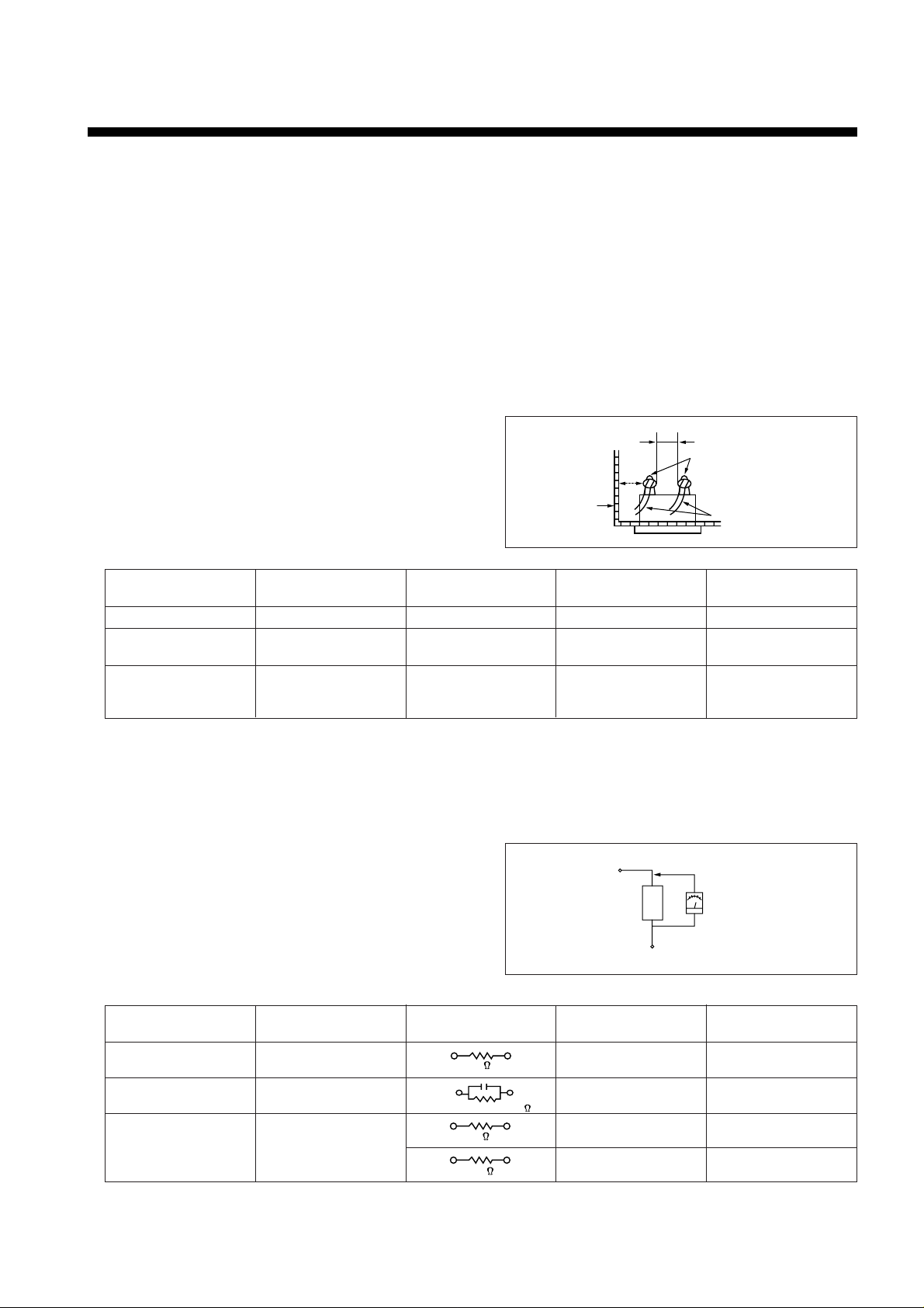
• Safety Check after Servicing
Examine the area surrounding the repaired location for damage or deterioration. Observe that screws, parts and wires
have been returned to original positions. Afterwards, perform the following tests and confirm the specified values in order
to verify compliance with safety standards.
1. Insulation resistance test
Confirm the specified insulation resistance or greater between power cord plug prongs and externally exposed parts of
the set (RF terminals, antenna terminals, video and audio input and output terminals, microphone jacks, earphone
jacks, etc.). See table below.
2. Dielectric strength test
Confirm specified dielectric strength or greater between power cord plug prongs and exposed accessible parts of the
set (RF terminals, antenna terminals, video and audio input and output terminals, microphone jacks, earphone jacks,
etc.) See table below.
3. Clearance distance
When replacing primary circuit components, confirm
specified clearance distance (d), (d') between soldered
terminals, and between terminals and surrounding
metalic parts. See table below.
Table 1: Rating for selected areas
* Class II model only.
Note: This table is unofficial and for reference only. Be sure to confirm the precise values for your particular country and
locality.
4. Leakage current test
Confirm specified or lower leakage current between B (earth ground, power cord plug prongs) and externally exposed
accessible parts (RF terminals, antenna terminals, video and audio input and output terminals, microphone jacks,
earphone jacks, etc.)
Measuring Method: (Power ON)
Insert load Z between B (earth ground, power cord plug
prongs) and exposed accesible parts. Use and AC
voltmeter to measure across both terminals of load Z.
See figure 2 and following table.
Table 2: Leakage current ratings for selected areas
Note: This table is unofficial and for reference only. Be sure to confirm the precise values for your particular country and
locality.
Fig. 2
AC Line Voltage Region
Insulation Dielectric Clearance
Resistance Strength Distance (d), (d')
100V Japan ≥1 MΩ/500 V DC 1kV AC 1 minute ≥ 3 mm
110 to 130V
USA &
– – –
900V AC 1 minute ≥ 3.2mm
Canada
* 110 to 130 V Europe ≥ 4 MΩ/500 V DC 3 kV AC 1 minute ≥ 6 mm (d)
200 to 240 V Australia ≥ 8 mm (d')
(a: Power cord)
AC Line Voltage Region
Earth Ground
Load Z Leakage Current (i)
(B) to:
100V Japan ¡ ≤ 1m A rms
Exposed accessible
parts
110 to 130 V USA & ¡ ≤ 0.5 m A rms Exposed accessible
parts
¡ ≤ 0.7 m A peak Antenna earth
110 to 130 V Europe ¡ ≤ 2 m A dc terminals
200 to 240 V Australia ¡ ≤ 0.7 m A peak
Other terminals
¡ ≤ 2 m A dc
Fig. 1
1k
1.5k
1.5kµF
2k
50k
d
Primary circuit termimals
Chassis
d'
a
Exposed
accessible
part
Z
Earth Ground
power cord plug prongsB
AC Voltmter
(high impedance)

1
TABLE OF CONTENTS
SECTION 1. CONTROLS AND FUNCTIONS......................................................................................................2~4
SECTION 2. ELECTRICAL ADJUSTMENTS
2-1. SERVO CIRCUIT ADJUSTMENT METHOD........................................................................................... .......................... 5
2-2. AUDIO CIRCUIT ADJUSTMENT METHOD..................................................................................................................6~8
2-3. PIF CIRCUIT ADJUSTMENT METHOD............................................................................................. ............................... 9
SECTION 3. TROUBLE SHOOTING FLOW CHART
3-1. POWER CIRCUIT......................................................................................................................................................10~11
3-2. LOGIC CIRCUIT.........................................................................................................................................................12~14
3-3. SERVO-SYSCON CIRCUIT ......................................................................................................................................15~19
3-4. AUDIO CIRCUIRT......................................................................................................................................................20~25
3-5. VIDEO CIRCUIT.........................................................................................................................................................26~31
SECTION 4. BLOCK DIAGRAM............................................................................................................................32~33
SECTION 5. CIRCUIT DIAGRAM
5-1. CONNECTION DIAGRAM.........................................................................................................................................34~37
5-2. POWER CIRCUIT (SMPS).........................................................................................................................................38~39
5-3. SYSCON CIRCUIT...........................................................................................................................................................40
5-4. LOGIC CIRCUIT.........................................................................................................................................................41~44
5-5. PIF & NTS & D/V INPUT SELECTOR CIRCUIT........................................................................................................45~46
5-6. AUTO-DETECT CIRCUIT.................................................................................................................................................47
5-7. VIDEO CIRCUIT ...............................................................................................................................................................48
5-8. AUDIO CIRCUIT...............................................................................................................................................................49
5-9. PRE AMP CIRCUIT..........................................................................................................................................................50
5-10. OSD CIRCUIT ................................................................................................................................................................51
5-11. WAVE FORM...........................................................................................................................................................52~55
SECTION 6. VOLT AGE CHAR T
6-1. IC VOLTAGE.............................................................................................................................................................. 56~64
6-2. TR VOLTAGE.............................................................................................................................................................65~66
SECTION 7. COMPONENTS LOCA TION GUIDE ON PCB (BOTTOM VIEW)
7-1. PCB HEAD-AMP..............................................................................................................................................................67
7-2. PCB SHUTTLE.................................................................................................................................................................68
7-3. PCB MAIN........................................................................................................................................................................ 69
7-4. PCB LOGIC................................................................................................................................................................70~71
7-5. PCB AUTO DETECT........................................................................................................................................................72
SECTION 8. DISASSEMBLY
8-1. PACKING AS.............................................................................................................................................................73~76
8-2. SET TOTAL ASSEMBLY........................................................................................................................................... 77~80
8-3. FRONT PANEL ASSEMBLY.....................................................................................................................................81~84
8-4. SHUTTLE STATION ASSEMBLY....................................................................................................................................86
SECTION 9. ELECTRICAL P AR TS LIST
9-1. STANDARD PART NUMBER CODING ..........................................................................................................................88
9-2. ELECTRICAL PARTS LIST......................................................................................................................................89~110
2
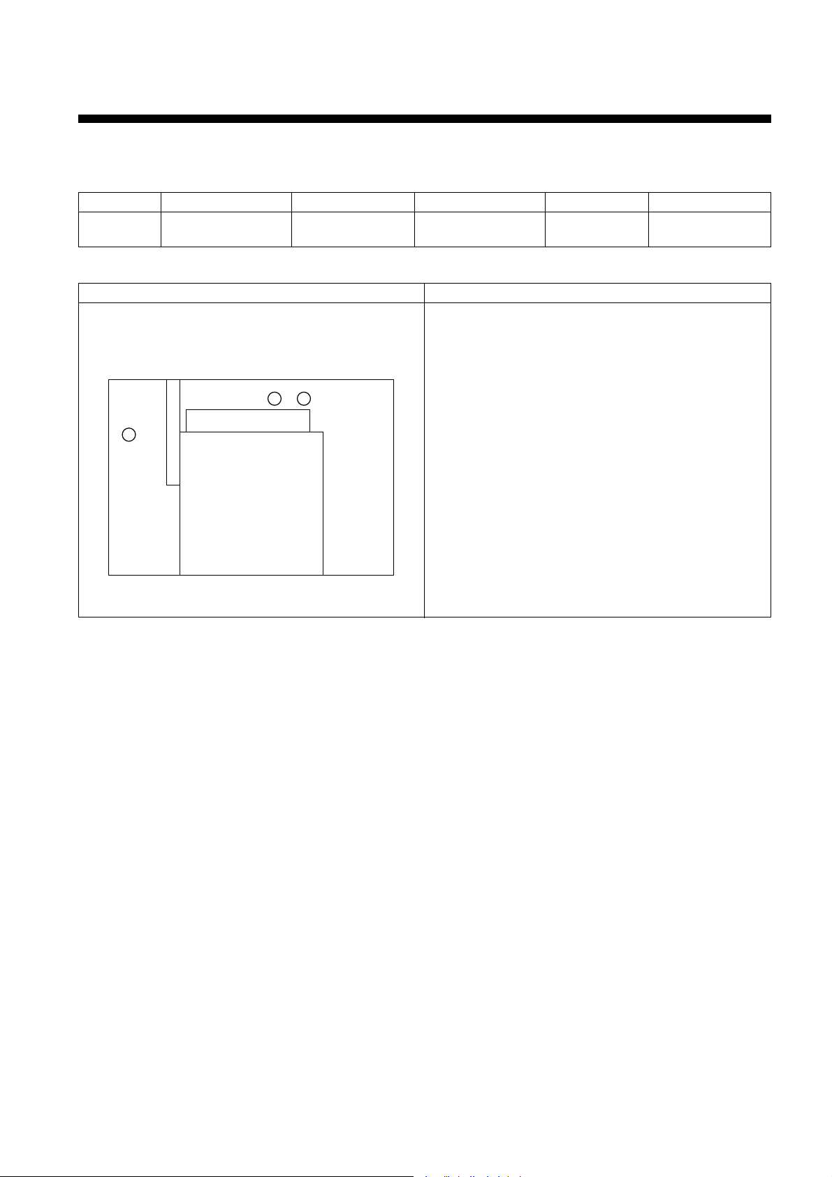
SECTION 1. CONTROLS AND FUNCTIONS
FRONT
DV -F803, 503 SERIES
EJECT
REC
POWER
PLAY
STOP
PAUSE
/STILL
CH.
REW
FF
OPEN
DV -F803
TAPE
NTSC
PAL
R
EJECT
REC
POWER
PLAY
STOP
PAUSE
/STILL
CH.
REW
FF
L
AUDIO
SYSTEM CONVERTION
NTSC
PAL
VIDEO IN
DV -F503
TAPE
NTSC
PAL
VIDEO AUDIO
AUTO
NTSC PAL
VTR SYSTEM
EJECT
REC
POWER
PLAY
STOP
PAUSE
/STILL
CH.
REW
FF
3
DV -F883, 683 SERIES
PAUSE
STILL
STOP
PLAY
CHANNEL
REC
POWER EJECT
F
F
R
E
W
+
–
OPEN
DV -F883
AUDIOVIDEO
TAPE
PALNTSC
LR
PAUSE
STILL
STOP
PLAY
CHANNEL
REC
POWER EJECT
F
F
R
E
W
+
–
SYSTEM
PALNTSC
DV -F683
AUDIOVIDEO
TAPE
PALNTSC
PAUSE
STILL
STOP
PLAY
CHANNEL
REC
POWER EJECT
F
F
R
E
W
+
–
SYSTEM
PALNTSC
4
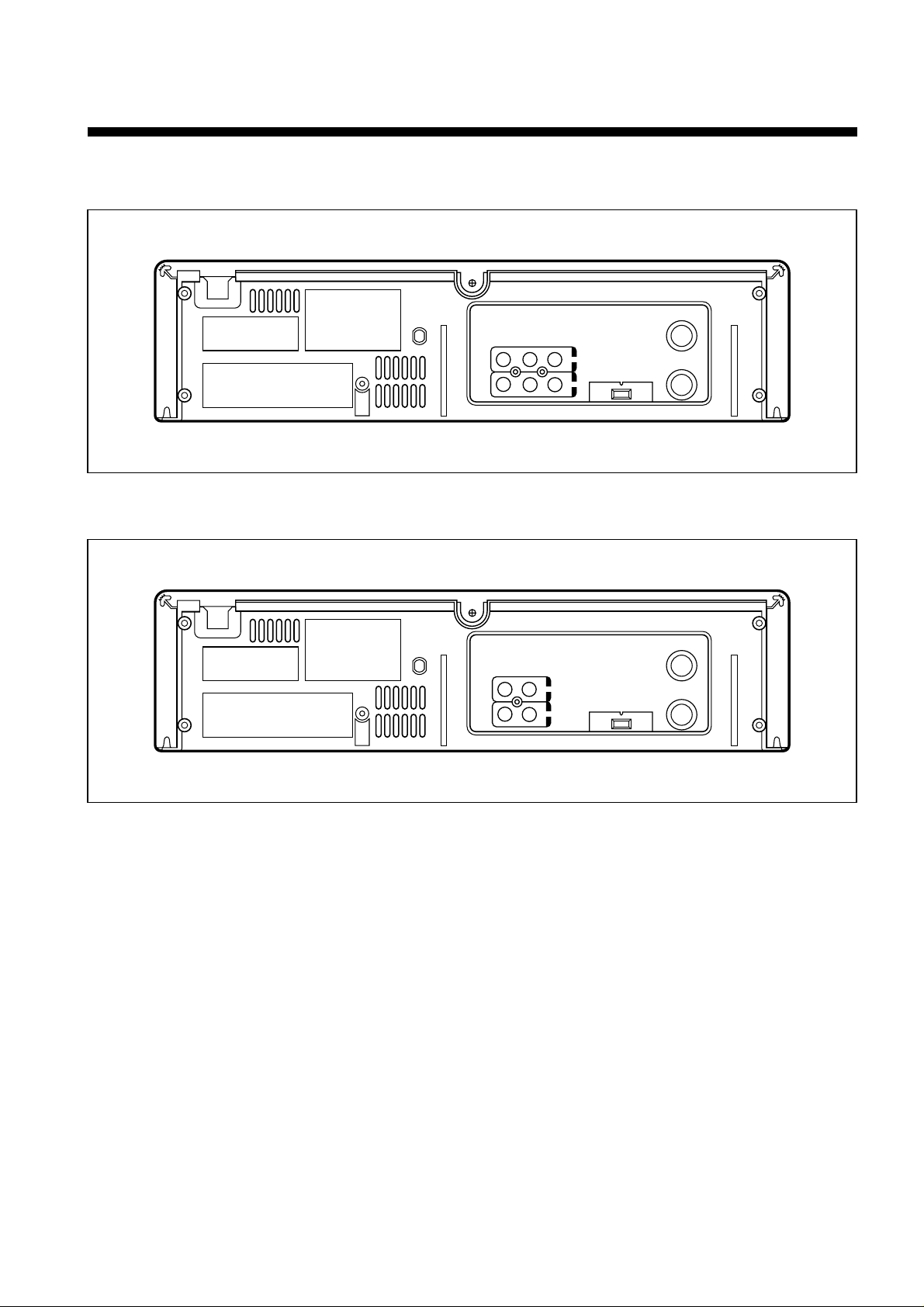
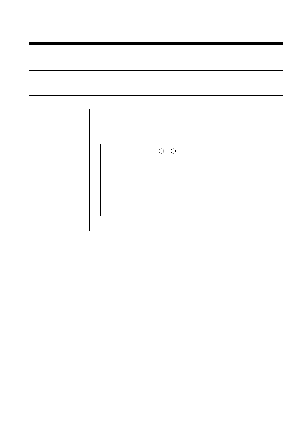
REAR
DV -F883, 803 SERIES
CH.3 CH.4
RF OUT
ANT.IN
OUT
IN
VIDEO AUDIO
LR
DV -F683, 503 SERIES
CH.3 CH.4
RF OUT
ANT.IN
OUT
IN
VIDEO AUDIO

5
SECTION 2. ELECTRICAL ADJUSTMENTS
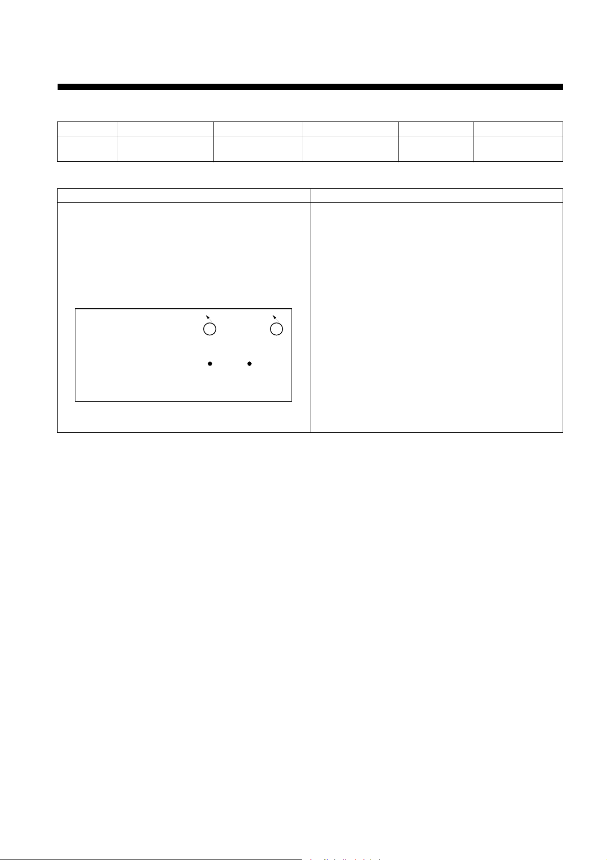
2-1. SERVO CIRCUIT ADJUSTMENT METHOD
1. PB Phase
• Adjustment Procedure
1. Set the oscilloscope to the CHOP mode. Connect the oscilloscope to check point and trigger the scope with CH1.
2. Adjust R595 to position the V-SYNC at 6.5±0.5H from the rising edge of sw pulse.
• Adjustment Inspecition Standard:
6.5±0.5H
Mode Adjustment Parts Check Point Test Equipments Test Tape Input Signal
CH 1: PT01 #
PLAY ! R595 CH 2: VIDEO Oscilloscope
DN-1
OUTPUT JACK
(Color Bar)
Location of Adjustment Parts Observation Waveform
H-Axis: 50us/div V-Axis: CH 1 ¡ 1.0v/div
CH2 ¡ 0.5v/div
MAIN PCB
T
U
HEAD-AMP / AUDIO
3
N
E
R
2 1
DECK
6
2-2. AUDIO CIRCUIT ADJUSTMENT METHOD
1. Audio REC Bias
• Adjustment Procedure
1. Set the TV/LINE to LINE mode
2. Connect the Audio level meter to both TP1 and TP2.
3. After inserting a blank tape, record in SP mode.
4. Adjust R292 to obtain 3.0±0.1mVrms.
• Adjustment Inspecition Standard:
In confirmation of Recording playback frequency characteristics, compared with 1KHz Recording-playback output level,
10KHz Recording-playback output level is higher than the standard, increase the record bias and if lower, decrease it.
Mode Adjustment Parts Check Point Test Equipments Test Tape Input Signal
+: TP1
REC @ R292 –: TP2 Audio level meter Blank tape Without signal
(A/C HEAD PCB)
Location of Adjustment Parts
MAIN PCB
T
U
N
E
HEAD-AMP / AUDIO
R
2 1
DECK
7
2. Audio Playback Frequency Characteristics
• Adjustment Procedure
1. Play back the test tape. Confirm the output level of 7 KHz is in the range of –1±3dB, compared with the output level of 1
KHz.
3. EE LEVEL
• Adjustment Procedure
1. Set the TV/LINE to LINE mode.
2. Connect the Audio signal generator to the AUDIO INPUT JACK.
3. Confirm the Audio output level –6±1.5dBm when you supply 1KHz (–8dBm) to the AUDIO INPUT JACK.
4. Insert a blank tape.
Record and play back the signal of 1KHz (–8dBm) (SP/EP MODE).
5. Confirm the Audio output level and Distortion meet the followings.
1) Audio playback output level
SP: –6±3dBm
EP: SP±3dBm
2) Audio distortion
SP: 3% maximum
4. Confirmation of Recording Playback Frequency Characteristics
• Adjustment Procedure
1. Set the TV/LINE to LINE mode.
2. Connect the Audio signal generator to the AUDIO INPUT JACK and Audio level meter to the AUDIO OUTPUT JACK.
3. Insert a blank tape.
Record the signal of 400 Hz and 10 KHz and 10 KHz in SP mode.
4. The output level of 10 KHz should be within –1±3dB to the output level of 400 Hz in the PLAYBACK mode (SP).
5. Insert a blank tape.
Record the signal of 400 Hz and 5 KHz (–20dBm) in EP mode.
6. The output level of 5 KHz should be within –1±3dB to the output level of 400 Hz in the PLAYBACK mode (EP).
Mode Adjustment Parts Check Point Test Equipments Test Tape Input Signal
Audio level meter
DN-1
PLAY Check NTSC Audio Output
DN-2
Mode Adjustment Parts Check Point Test Equipments Test Tape Input Signal
PLAY Audio level meter
REC
Check NTSC Audio Output
Distortion meter
Blank tape 1KHz -8dBm
Mode Adjustment Parts Check Point Test Equipments Test Tape Input Signal
REC Audio level
PLAY
Check NTSC Audio Output
meter
Blank tape -20 dBm
8
5. Hi-Fi Carrier (DV-F803M/883M)
• Adjustment Procedure
1. Preparation
1) Set the TV/LINE to LINE Mode.
2) Supply the input signal in the OPEN state.
2. Adjustment
1) Set the VCR to the REC Mode (SP).
2) Connect the frequency counter to TP902 (1.3MHz) and TP901 (1.7MHz).
3) Adjust R991 to set the frequency of TP902 for 1.3±0.01MHz.
4) Adjust R993 to set the frequency of TP901 for 1.7±0.01MHz.
3. Adjustment Inspection Standard:
1.3±0.01 MHz (TP902)
1.7±0.01 MHz (TP901)
Mode Adjustment Parts Check Point Test Equipments Test Tape Input Signal
R991 TP902
REC
R993 TP901
Frequency counter Blank Tape No Signal
Location of Adjustment Parts Observation Waveform
Horizontal Axis: S/DIV
Vertical Axis : V/DIV
Hi-Fi/PRE AMP PCB (COMPONENTS SIDE)
(1.3M) (1.7M)
R991 R993
TP902 TP901
9
2-3. PIF CIRCUIT ADJUSTMENT METHOD
1. STEREO (DV-F803M/883M)
• Adjustment Procedure
1. Connect the output of US 5CH (L=1KHz 100% MOD, R=nonsignal) to ANT IN OF TMI.
Then RF signal input is 93dBu.
2. Connect audio output L and R to AC volt meter 1CH and 2 CH.
3. Turn R191, confirm if L output changes.
Fix the minimum point of R output.
* The condition of US 5CH: Color Bar: 87.5% modulation, 72dBuV
Audio: L CH=1KHz, 100% MOD, R CH=nonsignal
Using equipment: Audio Signal Generator, MPX equipment, RF Modulator
• Adjustment Inspecition Standard: The minimum point of R output.
Mode Adjustment Parts Check Point Test Equipments Test Tape Input Signal
EE Audio
MODE
# R191
Output-R
AC Volt meter US 5CH
Location of Adjustment Parts Observation Waveform
MAIN PCB
T
U
HEAD-AMP AND HiFi
3
N
E
R
2 1
DECK
10
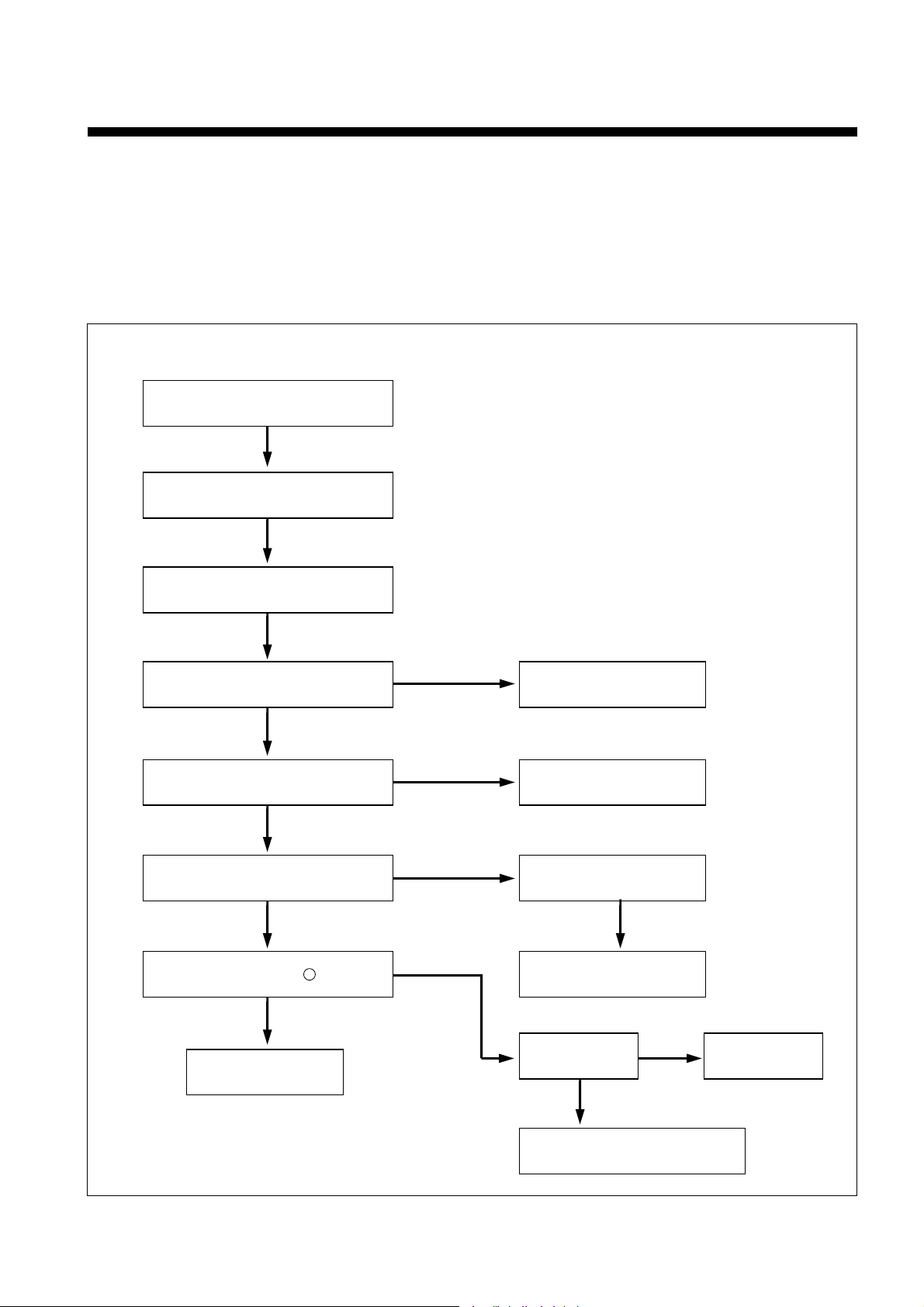
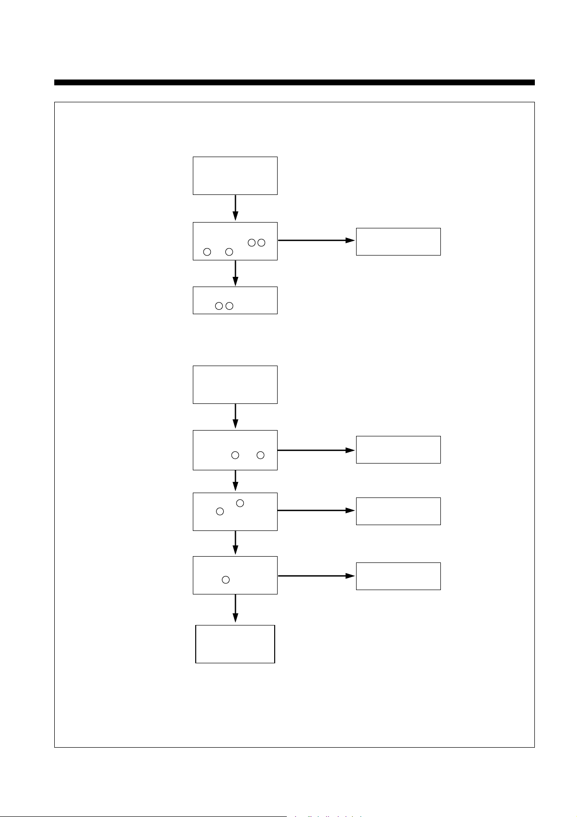
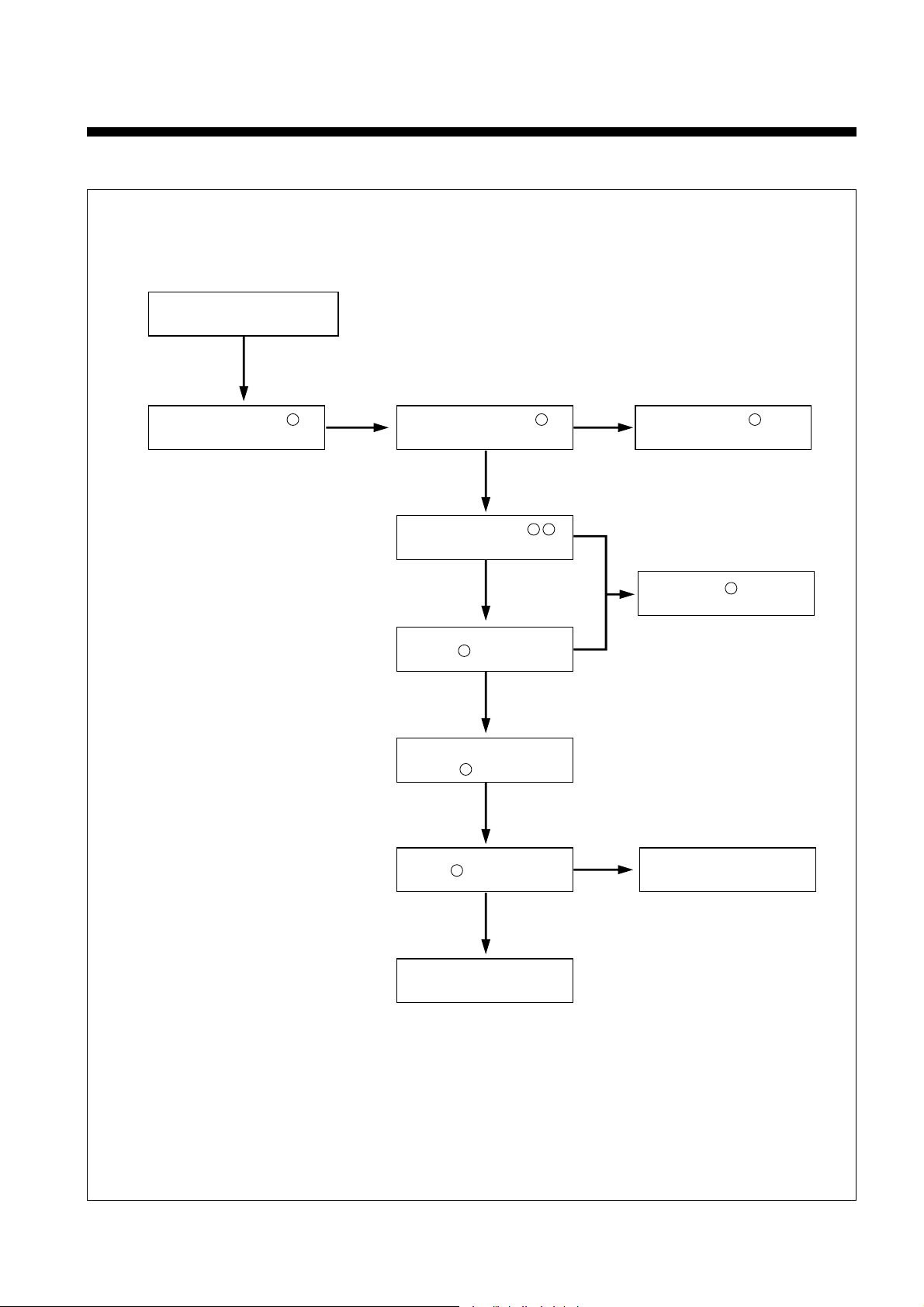
SECTION 3. TROUBLE SHOOTING FLOW CHART
3-1. POWER CIRCUIT
• When change the parts which are out of order, first, remove the power plug from the socket and then discharge the
voltage across between both terminals of C807. (Use an external scores of KΩresistance)
• When check the primary circuit by using the oscilloscopes insulate the oscilloscope surely. (Use the isulating
transformer) and must connect GND into the primary GND (But there is no connection when check the secondary
circuit).
• When change IC801, check FUSE and Cement resistance surely.
Prepare the instrument
connecting the insulating trans.
Check F801 FUSE.
Is voltage applied to D801?
Is voltage applied to the
both terminals of C807?
Check voltage of Q801 Gate.
4
Is voltage output from pin of IC801?
Check Q801.
Check D801, L801 & L802.
Check R802.
Check R803, 805, 823
814, 806 & C817.
Check Q802, 803,
D802, R809.
Check IC801. Change IC801.
Check the Secondary circuit.
NO
NO
NO
NO
NO
YES
YES
YES
YES
YES
YES
YES
YES
NO output Voltage.
A. CHECKING THE PRIMARY CIRCUIT.
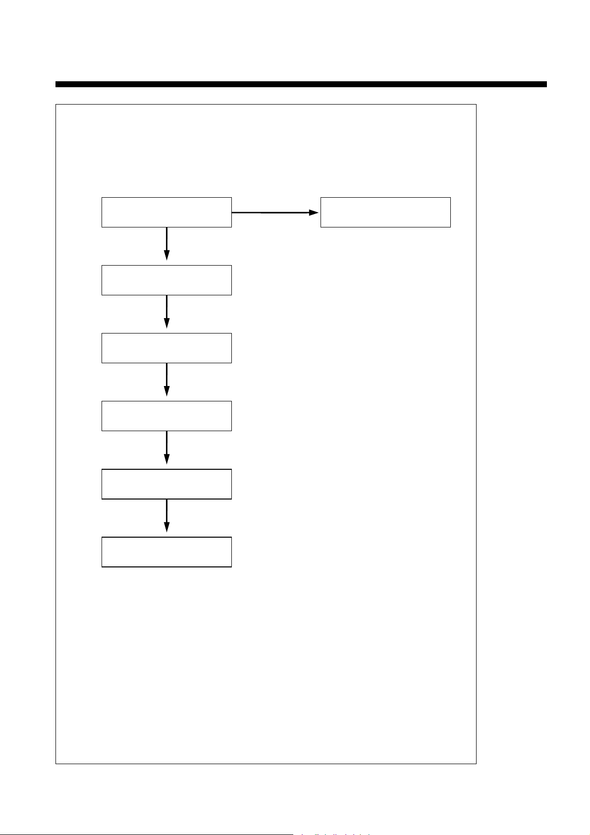
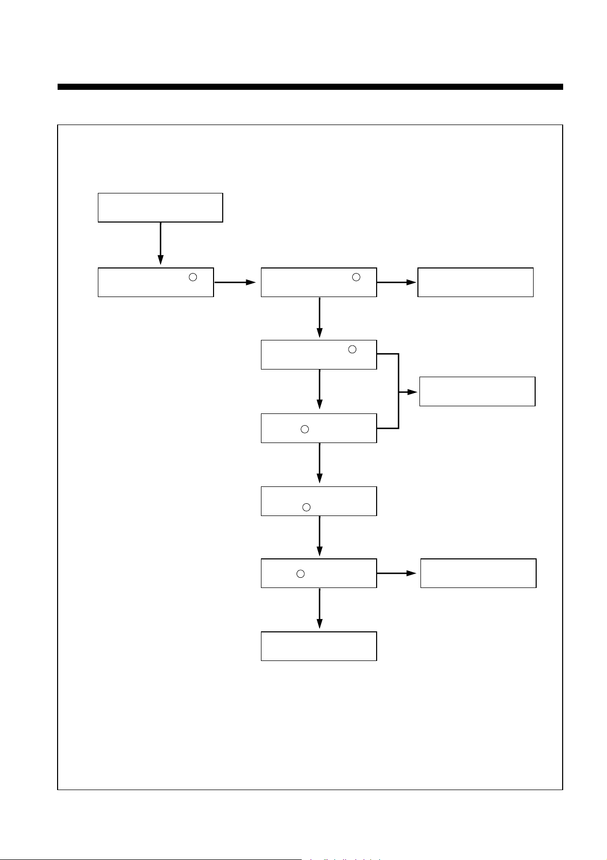
11
IS DZ805, DZ807 Short?
Check each votage.
Check Trans output of
No output stage.
Check the DIODE of
NO output stage.
Check COIL, C of
No output stage.
Check the environmental
terminals of IC801.
Change DZ805, DZ807 and check
IC801 and primary circuit.
YES
NO
YES
YES
YES
YES
B. CHECKING THE SECONDARY CIRCUIT.
12
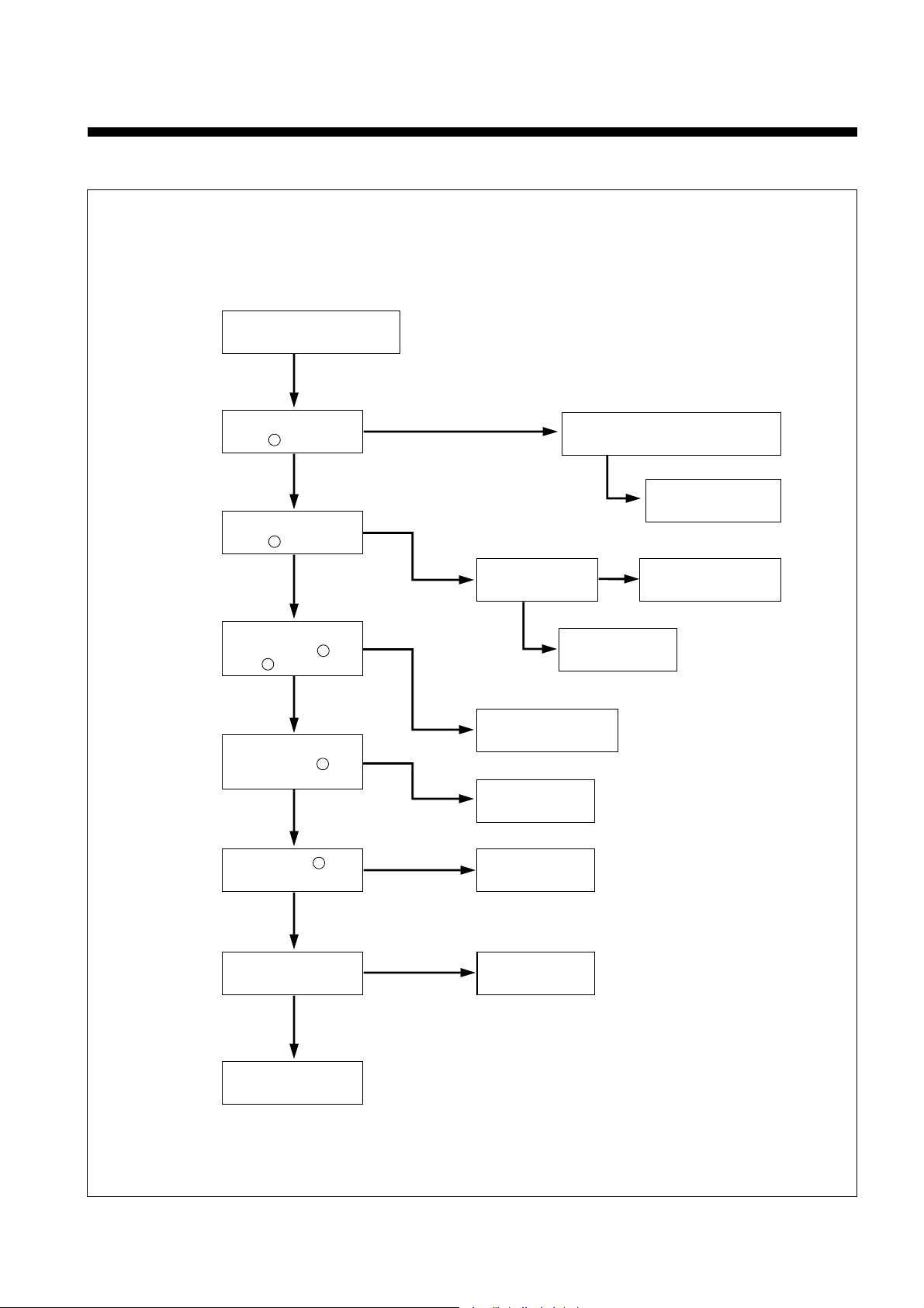
3-2. LOGIC CIRCUIT
Digitron does
not operate & is not good.
Is+5V supplied to
pin of IC701?
8
Is-28V supplied to
pin of IC701?
11
Are -25.8 and -21.2V
supplied to pin and
of G701?
1
46
Are CLK signals
supplied to pin
of IC701?
40
Is 5V at pin of
IC701?
7
Check X701.
Check IC701
and change.
CHECK D815and Primary
power circuit.
Check the
DZ601.
Check D814 and
primary power circuit.
Change DZ601.
Check the Trans output
and DZ601.
Check IC601.
Change IC702.
Change X701.
YES
YES
YES
YES
YES
YES
NO
NO
NO
NO
NO
YES
NO
NO
A.
YES
Check the connector
and pattern.
13
Digitron is lit but
key do
not operate.
Is each key pulse
applied to pin ,
and of IC701?
2 3
12 13
Check key matrix
circuit.
Check the pin serial of
pin , of IC701.
38 39
It has not power-failure
compensation
operation.
When disconnecting
the power cord,is 5.4V
at pin and
of IC601?
26 81
Do pin and
of IC601
oscillate?
42
Is +5V applied to
pin of IC601?
37
Check IC601.
Check C605.
Check X602
environmental circuit.
NO
YES
YES
YES
YES
NO
NO
NO
B.
C.
43
Check the IC606
RESET circuit.
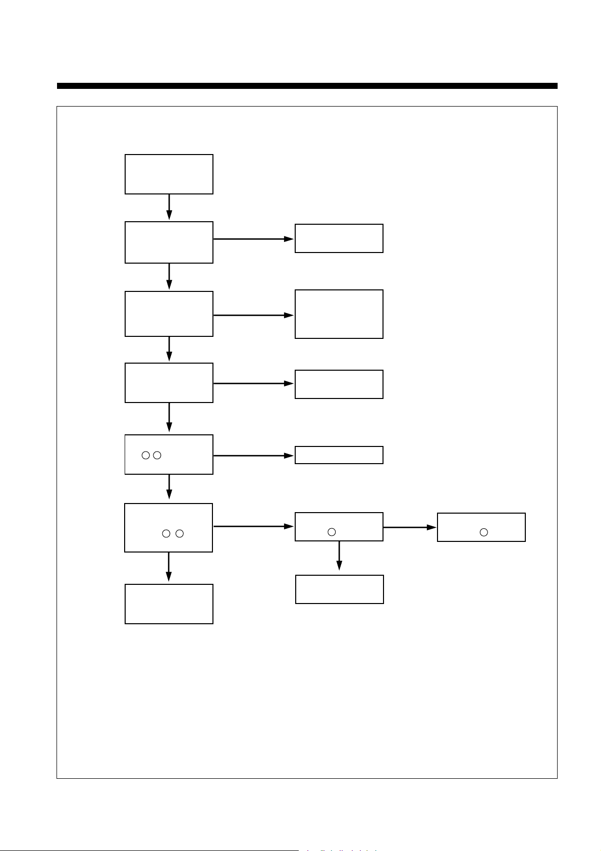
14
When change the
channel broadcast
signal is not received.
Is the external ANT.
connected to RF IN of
VCR and RF OUT
of TV?
Is the Power of VCR
ON and the VCR
indicator lit on the
digitron?
Does the TV channel
correspond to VCR
(3 or 4) channel?
Change and check the
connection of CABLE
Power On and select
the VCR mode by
pressing the
TV/VCR key.
YES
YES
YES
YES
NO
NO
NO
D.
Set the TV channel to
VCR (3 or 4) channel.
Check the Video,
Audio outputsignal of
pin , of
TMI BLOCK.
Check the TMI
BLOCK.
Check IC601
Check the
Video circuit.
Check the
IC601 pin.
Is the output of pin
, of IC601
normal?
100 98
YES
NO
44
14 18
Is the signal applied
to pin of IC151?
NO
YES
NO
YES
14
15
91
The voltage of pin
of IC601 is not
changed.
Is CTL pulse input
to pin and of
IC601?
71 72
73
Check and
re-adjust the
Path of Deck.
Check circuit
adjacent to IC601.
Check R523, R524
C508, C509.
check R518
and C511.
Check IC601.
YES
YES
YES
YES
YES
YES
YESNO
NO NO
NO
NO
NO
A.
Playback picture
is not good.
Noise appears
although adjusting
tracking.
Is CTL pulse applied
to pin of IC601?
Noise shakes up
and down on the
screen.
Adjust
tracking.
CTL HEAD height is
normal and there is
not dust.
Adjust the HEAD
height and remove
dust.
Noise appears
although change
cassette tape.
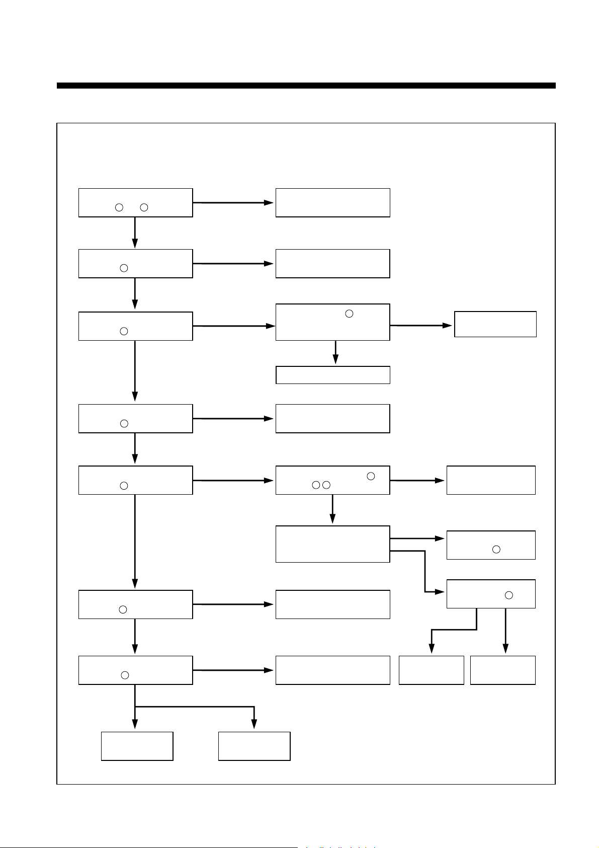
3-3. SERVO SYSCON CIRCUIT
16
Playback picture
is not good.
Noise appears
on the screen
whole.
Is Enve.waveform
supplied to at
pin of PT01?
4
Are SW pulse and
HA SW applied to
HEAD-AMP circuit?
Check VIDEO circuit.
Auto stop during
playback.
Is Reel pulse
applied to pin and
of IC601?
5
6
Check Flow A.
Is SW pulse supplied
from pin of IC601?
18
Check D.PG input
and connector.
Check pattern.
Check connector, Head
Amp and Head dust.
Change Head.
Check REEL
sensor part.
Is D.FG applied to
pin of IC601?
Check connector
and D.FG circuit.
Check IC601.
NO
YES
YES
YES
YES
YES
NO NO
NO
NO
NO
YES
NO
67
B.
C.

17
Drum M/T loading stops.
Is Motor 12V supplied?
Is pin D.FG of
IC601 supplied?
Is pin D.PWM (pin )
of IC601 supplied?
Check connector
and Motor.
Is the input of pin
of P501 2V-3.5V?
Is pin of P601 2.5V?
Is pin (C.PWM)
of IC601 Supplied?
Check connector
and Motor.
67
4
1
18
3
Check power circuit.
Check C505, R506, R507
and C516.
Check IC601.
Check power circuit.
Check circuit of R510,
R511, R512.
Check R508, R509.
Check IC601.
YES
YES
YES
YES
YES
YES
YES
NO
NO
NO
NO
NO
NO
NO
Capstan M/T loading stops.
Is Motor 12V supplied?
D.
E.
18
Drum M/T and Capstan M/T rotate
at regular speed (In REC mode).
Is C. Sync applied to
pin of IC601?
93
Check Motor.
Check C. Sync of
VIDEO IC and Pattern.
Emergency mode when
connecting the Power cord.
Is EVER 5V supplied?
Does X601 crystal oscillate?
Do S/DATA, CLK and RDY
Signals of IC601 exchange
with IC701?
Is CAM SW DATA Correct?
Check IC602.
Check IC 601.
Check power circuit.
Check IC601 and X601.
Check IC701 when CS Signal
is supplied.
Check IC601 when CS Signal
is not supplied.
Recheck connector
and CAM SW contact.
YES
YES
YES
YES
YES
YES
NO
NO
NO
NO
NO
F.
G.
NO
19
Cassette is not
inserted.
Is Motor 12V supplied?
Check power circuit.
Is there the changes
CAM DATA when CST IN?
Is 7.5V applied to pin of
IC602 when CST IN?
4
Chek IC602.
Check connector. Check DECK part.
Is 5V supplied at
pin of IC601?
Check PATTERN.
47
Check IC601.
H.
NO
YES
YES
YES
NO NO
NO NO
YES
20
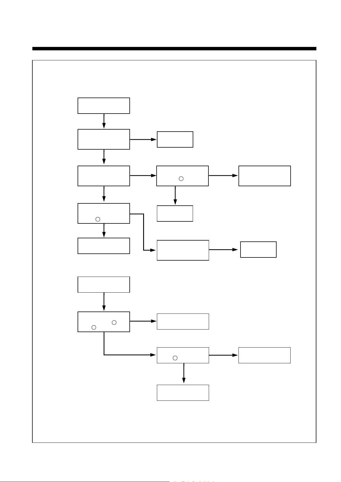
3-4-1. AUDIO CIRCUIT (Hi-Fi)
No
No
No
No sound in the E-E mode
A.
Is 12V applied to pin
of IC901?
Yes
Is 5V applied to pin ,
, of IC901?
Yes
Check
POWER circuit
Check SYSCON circuit
1
16
26 33
No
Is signal input into
pin , of IC901
in LINE mode?
Yes
Check input jack
3
46
Yes
Is there output at
pin , of IC901?
Yes
Check out JACK
Change IC901
No
Is pin of IC901 0V?
36
58 62
No
Is signal input into
pin #, [ of IC901
in TV mode?
Yes
Check IC151

21
No sound in the playback
mode after reccording.
Is the signal applied to
pin of IC901?
46
Is 5V applied to
pin of IC901?
6
Is there output at
pin of IC901?
55
Does T201 oscillate?
Check circuit adjacent
to IC151.
Check IC601.
Check IC901.
Is the voltage above 12V
at pin of T201?
Check Q212
collector:above 12V
Base:0V
Check T201.
Is record current
3.0mVrms?
Is pin of IC901 0V?
2
Clean HEAD.
Asjust Record current.
Check IC901.
Check IC901.
Check Q212, Q213
NO
YES
YES
YES
YES
YES
YES
NO
NO
NO
YES
NO
NO
NO
NO
YES
3
B
22
No
Check C905
No
Check IC601
No
Check the ICH01
of PRE-AMP circuit
No
No Hi-Fi Sound
in playback mode
B.
Is the ENVE level of pin
IC901 more than 280mVp-p?
Yes
Is A SW PULSE input into
pin of IC901?
Yes
Is pin of IC901 5V?
Change IC901
Is the ENVE. input into
pin of IC901?
27
Yes
23
25
Yes
Change
IC901
25
23
3-4-2. NORMAL AUDIO CIRCUIT (Hi-Fi NOMAL P AR T)
No sound in the playback mode.
62
Is the output at pin
of IC901?
Is 12V applied to pin
of IC901?
Check P901 pin and
power circuit.
1
Is 5V applied to pin ,
of IC901?
16
Is pin of P901 0V?
6
Is there Audio output
pin of IC901?
50
Is pin of IC901 GND?
2
Check P601
and AC Head.
Check pin of P902
and power circuit.
Check IC901.
NO
YES
NO
YES
YES
YES
YES
NO
NO
NO
A
8
33
9
24
3-4-3. NORMAL AUDIO CIRCUIT (DV-F683M/503M)
No sound in the playback mode.
22
Is the output at pin
of IC201?
Is 12V applied to pin
of IC201?
Check Q205
7
Is 5V applied to pin
of IC201?
11
Is pin of IC201 0V?
24
Is there Audio output
pin of IC201?
10
Is pin of IC201 GND?
3
Check P601
and AC Head.
Check IC601.
Check IC201.
NO
YES
NO
YES
YES
YES
YES
NO
NO
NO
A
25
No sound in the playback
mode after reccording.
Is the signal applied to
pin of IC901?
16
Is 5V applied to
pin of IC201?
24
Is there output at
pin of IC201?
21
Does T201 oscillate?
Check circuit adjacent
to IC151.
Check IC601.
Check IC201.
Is the voltage above 10 V
at pin of T201?
Check Q201
collector:above 10V
Base:0V
Check T201.
Is record current
3.0mVrms?
Is pin of IC901 0V?
1
Clean HEAD.
Asjust Record current.
Check IC201.
Check IC201.
Check Q201.
NO
YES
YES
YES
YES
YES
YES
NO
NO
NO
YES
NO
NO
NO
NO
YES
3
B
26
3-5. VIDEO CIRCUIT
Is video signal input
into pin and of IC151?
3 5
Is 12V supplied at
pin of IC151?
16
Is signal output from
pin of IC151?
16
Is signal input into
pin of IC301?
13
Is signal output from
pin of IC301?
17
Check PIF circuit
and LINE IN JACK.
Check ON/OFF 12V circuit.
Check IC601 pin.
Tuner mode : H
Line mode : L
Check PCB pattern.
Is 5V supplied to pin
and , of IC301?
14
39
Check
power circuit.
Check D301 (+) port
EE mode : L
PB mode : H
Check
IC601 pin.
29
Check IC301 pin.
Is signal input into
pin of ICS01?
18
Is signal output from
pin of ICS01?
16
Check PCB pattern.
Check OSD circuit.
RF out Line out
YES
YES
YES
YES
YES
YES
YES
YES
NO
NO
NO
NO
NO NO
HIGH
LOW
A.EE MODE PIcture N.G
NO
YES
Change IC151.
Change IC601.
NO
NO
44
41
Change IC301
Check
PCB pattern
HL
18
27
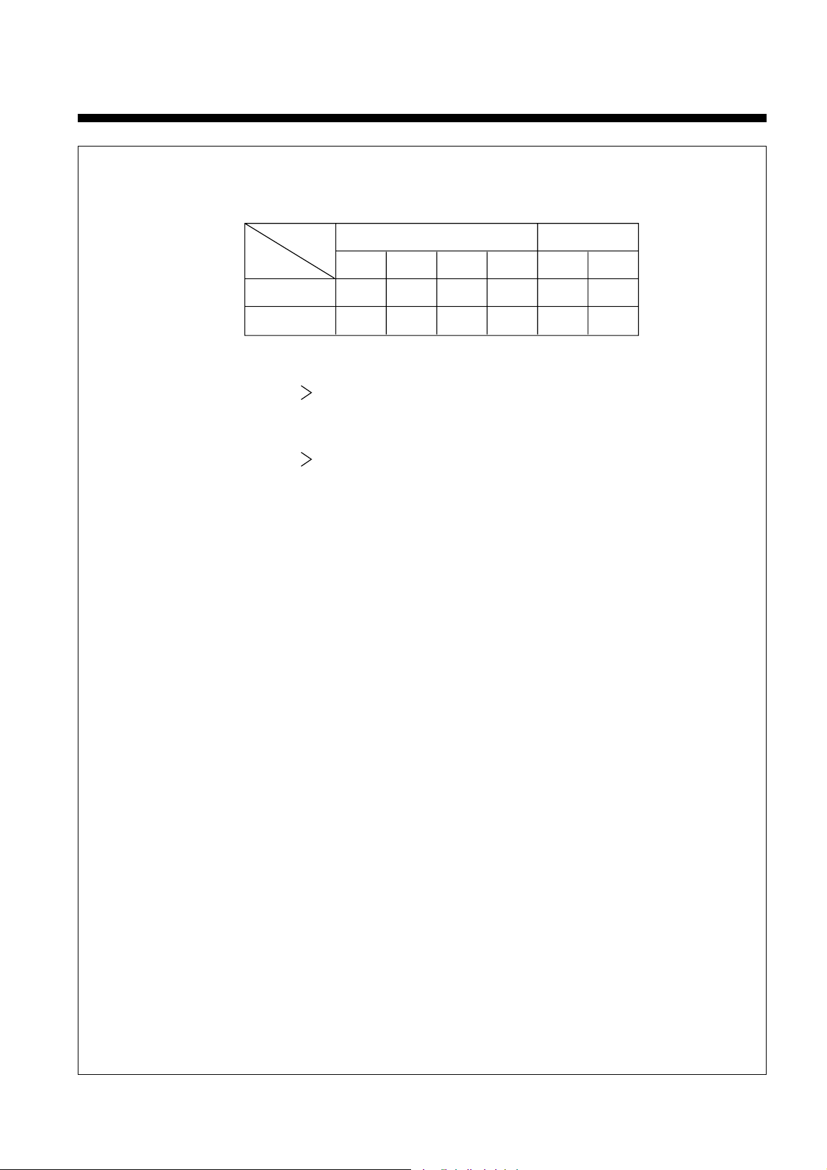
B . MODE TABLE.
PIN NO
IC301 IC302
NTSC MODE
PAL-M MODE
24 30 32 41 5 20
HXHHHH
HXLHHL
IC301 =
IC302 %
IC301 e
IC301 r
IC302 0
IC301 O
60Hz(H)
NAP
NTSC. H/PAL(L)
Filter change 3.58(H)
 Loading...