

Page 1

OSDPC78001
(7 Inch) LCD Color Monitor &
DVD Player
DPC-7800NT (2708ED)
DEC. 2006
Page 2

(7 Inch) LCD Color Monitor & DVD Player
MODEL : DPC-7800NT(2708ED)
CONTENTS
----------------
Specification.......................................................…...............................................…………….…..
Block Diagram...................................…................................................................…………….…..
General Alignment Instruction.......................................................................……….…….....…
2~3
4~5
6
Troubleshooting...........................................................................................…...……………...…..
Printed Circuit Board........................................................................................……………...…...
IC Block Diagram & Description.........................................................................…………..…..
Explode View........................................................................................................…………......….
Schematic Diagram.........................................................................................…………….....…..
7~8
9~13
14~31
32
33~42
Page 3

SPECIFICATION
LCD
Description Condition Unit Limit Nominal
Headphone Output 1kHz 0dB mW 3±2 3
Headphone Noise No Signal mV <1mV <1mV
SPK MAX
Output(DVD)
SPK MAX Output(AV
IN)
LINE OUT Distortion 1kHz 0dB/8ohm % ≤0.3 0.3
REF THD 1kHz 0dB % 3 1
Headphone S/N Infinity zere/-dB/L&R∝ dB ≥50 ≥50
Luminance(MAX) White Signal LUX 300±50 300
Luminance(8step) White Signal LUX 250±50 250
Luminance(MIN) White Signal LUX 100±50 100
L 1kHz 0dB mW 600±100 600
R 1kHz 0dB mW 600±100 600
L 1kHz 0dB mW 600±100 600
R 1kHz 0dB mW 600±100 600
20Hz dB ±3 0
LINE OUT RESP(8ohm)
Headphone RESP
125Hz dB ±3 0
10kHz dB ±3 0
20kHz dB ±3 0
20Hz dB ±3 0
125Hz dB ±3 0
10kHz dB ±3 0
20kHz dB ±3 0
-2-
Page 4

DVD
Description Condition Unit Limit Nominal
Video Signal Level Vp-p 0.7±0.1 0.7
SYNC Level Vp-p 0.3±0.1 0.3
Video out level
75% color bar/75ohm
Vp-p 1.0±0.2 1
Video out level(Unload) 75% color bar Vp-p 2.0±0.2 2
CD 1kHz/0dB/10K V 0.6±0.2 0.7
Audio out level
DVD 1kHz/0dB/10K V 2+0/-0.6 1.5
LINE OUT LEVEL 1kHz/0dB/10K V ≥2.8 3.6
20Hz dB ≤±3 0
FREQ RESP (DVD)
(20Hz~20kHz)
125Hz dB ≤±3 0
10kHz dB ≤±3 0
20kHz dB ≤±3 0
Signal-to-noise radio Infinity zere/-dB/L&R∝
dB ≥60 ≥60
Audio distortion&noise (DVD) 1kHz/0dB/L&R dB ≤-65 -65
Dynamic range (DVD) 1kHz/-60dB dB ≥85 ≥85
R/L Cross sound (DVD) 1kHz/0dB/L&R dB ≥45 ≥45
1kHz Channel unbalance 1kHz/0dB/L&R dB ≤3 0
Power Consumption Standby W ≤1 ≤1
DC 9V Rating W ≤12 ≤12
ECC Entircity A BEX TDV-552 um ≥100 100
Scratch A BEX TDV-541 mm ≥1.6 1.6
Black dot A BEX TDV-545 mm ≥ф0.8 0.8
Finger Print A BEX TDV-545 um ≥ф65 65
Vertical deviation A BEX TDV-533 mm ≥0.6 0.6
Note: Nominal specs represent the design specs. All units should be able to approximate these. Some will exceed
and some may drop slightly below these specs. Limit specs represent the absolute worst condition that might still
be considered acceptable. In no case should a unit fail to meet limit specs.
-3-
Page 5
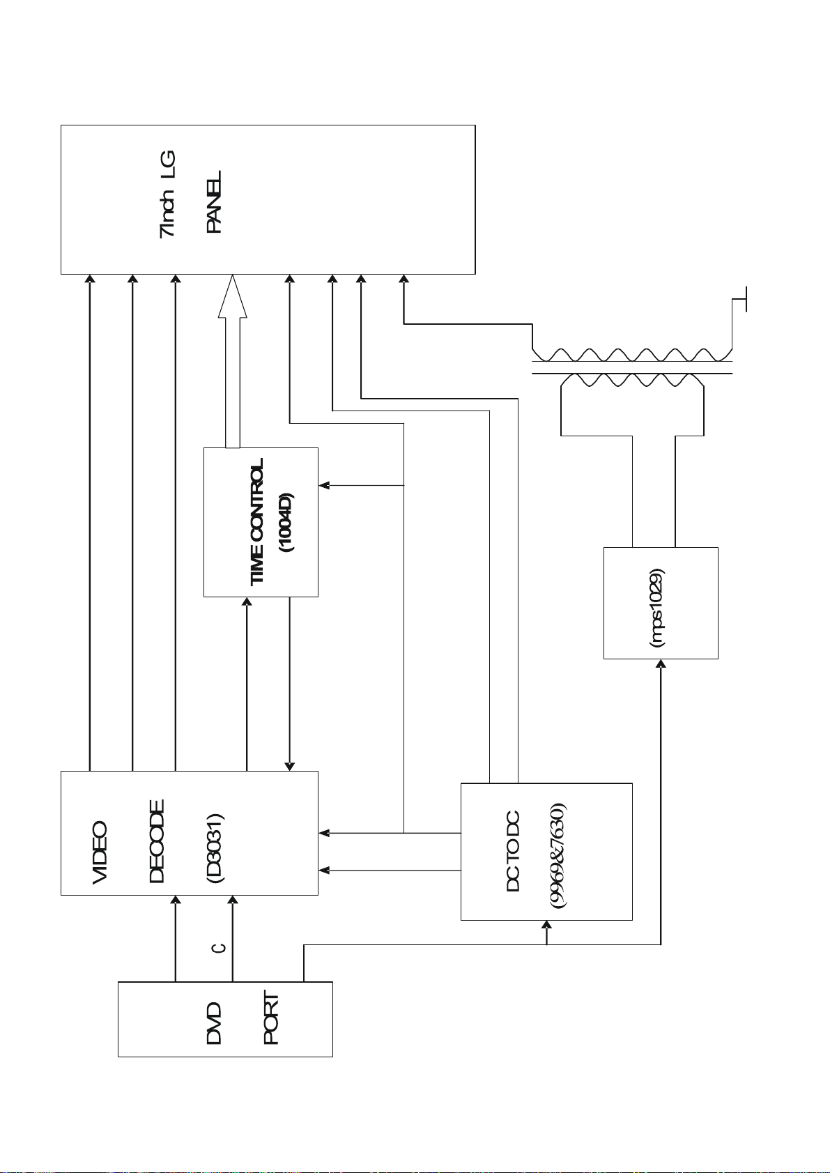
LCD
O
A
C
BLOCK DIAGRAM
DC T
R
G
B
SYNC
FRP
-13V
15V
5V
9V
7.5V
Y
9V
-4-
Page 6
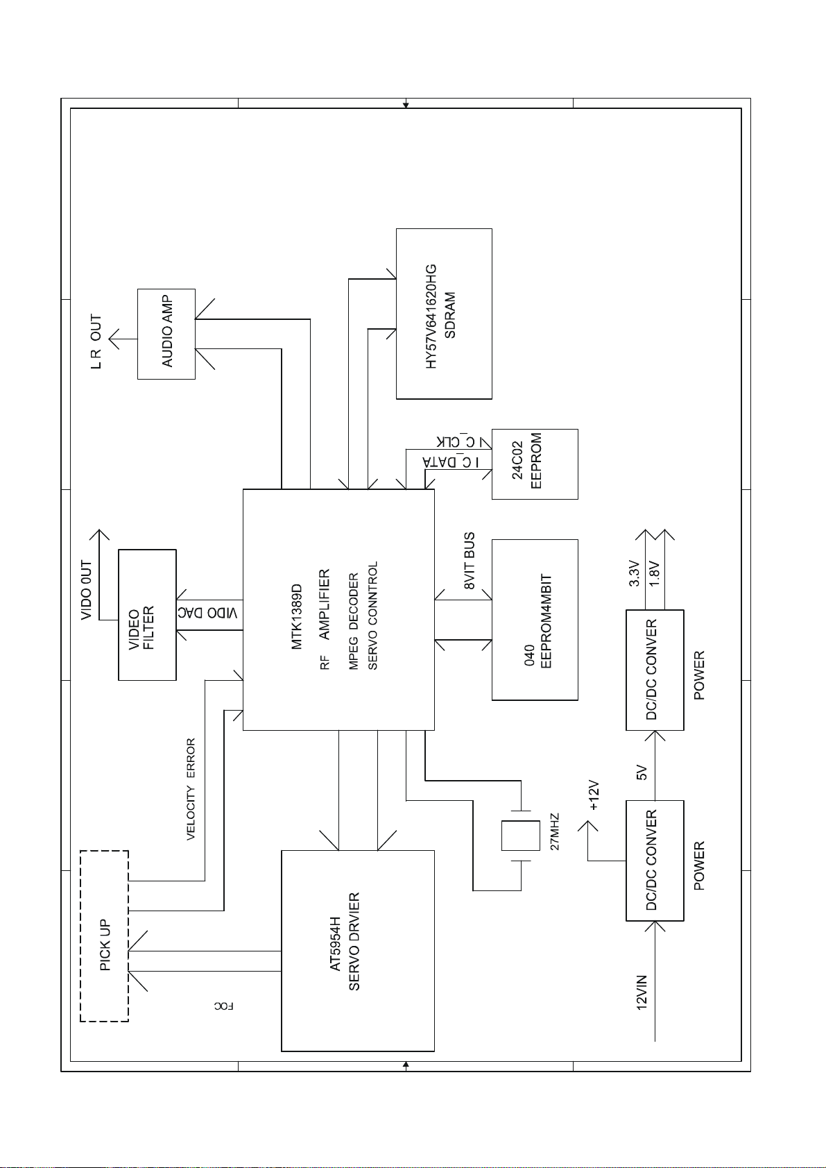
DVD
4332211DDCCBB
A
U
S TRACK
DRIVE
R
4
FE TE DRIVER
SPINDLE
5
SLED
A
5
-5-
Page 7

GENERAL ALIGNMENT INSTRUCTION
The Main PCB of Monitor Modification:
1. Input voltage is 6.8V-16V, input signal is test circuit BY 5418.
2. Adjust VR1 to get horizontal phase shift and test point: 28.9MHz
3. Adjust VRB4 to get good performance..
The main PCB of DVD Modification:
1. Adjust the brightness to the brightest by VR, adjust video pattern’s color to white, test the screen
Brightness is 200±102 LUX.
With luminometer You can adjust R66 to get this standard.
-6-
Page 8

LCD
SYMPTOM CAUSE REMEDY
LCD MONITOR PART
TROUBLESHOOTING
1) Picture distortion
2) No Picture
3) No Picture, Picture no
Good
4) Luminesce no good
5) Color is no good
6) SYNC no good
7) NO Picture
8) Picture no good
& Defective IC T110 (U301).
& Defective IC201 (D3031).
& Defective IC1 (CSC3414A). & Replace IC1 (CSC3414A).
& Defective IC201 MPS1029.
& Defective X201.
& Defective IC101 CSC1004D.
& Defective Q10 EL7630. & Replace Q10 EL7630.
& Defective CON4. & Replace CON4.
& Replace IC T110 (U301).
& Replace IC201 (D3031).
& Replace IC201 MPS1029.
& Replace X201.
& Replace IC101 CSC1004D.
9) Brightness no good
& Defective ICP1 SS9969. & Replace ICP1 SS9969..
-7-
Page 9

DVD
DVD PART
SYMPTOM CAUSE REMEDY
1) No Power
2) No Picture
3) No Sound
4) Sound no good
& Power source is not correct.
The positive and negative does not
match the unit.
& Power button defective.
& Defective T3 (24C02).
& Defective IC MTK1389D E/E.
& Defective U8 (4558D).
& Defective U6 (TDA2822)
& Defective U26 (TEA2025B)
& Defective U8 (4558D).
& Replace power source.
& Charge the position of positive
and negative.
& Replace power button.
& Replace T3 (24C02).
& Replace IC MTK1389D E/E.
& Replace U8 (4558D).
& Replace U6 (TDA2822)
& Replace U26 (TEA2025B)
& Replace U8 (4558D).
5) Can not read DISC
6) No key function
7) No remote control
function
& Defective U6 (TDA2822)
& Defective U26 (TEA2025B)
& Defective U3 (AT5654H).
& PICK-up Laser is defective.
& Replace U6 (TDA2822)
& Replace U26 (TEA2025B)
& Replace U3 (AT5654H)
& Replace pick up.
& Defective IC MTK1389D E/E. & Replace IC MTK1389D E/E.
& Defective IR1.
& Key is Defective.
& Replace IR1.
& Replace keys.
-8-
Page 10
IC201 D3031
INVIN
V
TBRIGHTBRIGHT
S/HS/HS/H
CIN
BLKFRPS/H PULSEGS/H PULSEGS/H PULSEG333534942303127283226292324
B DC DETB OUTG DC DETG OUTR DC DETR OUTSYNC.I
NSYNCOU
T
10BRIGHTBRIGHTSUBBSUB BRIGHTRRGBAMPLITUDE
γ1γ
γ γγγ
IC BLOCK DIAGRAM & DESCRIPTION
2
CONTRAST
PEAK LIMIT
21 2219 203637384846474561
S/H
INV
BRIGH
VREF
SEP
SYNC
SYNCSEP
PICTUREAGC
FILTER
OUT
AGC
CLAMP
COLOR
TRAPH FIL OUT
SW
BGPGEN
PICTURE
AGCAMP
AGCDET
COMP
TRAP
BGP
CLAMP
COLOR
Y/C
P
REG3
N
COMP
Y/C
HPF
P
KIL.LER
N
2
H.FILTER
3
REG2
REG1
41
ACC
COMP
5
ACC.DET
Y/C
APC
VCO
15
14
16
FADJ
VIDEO IN
ACC.FIL
APC.FH
VCO IN
VCO OUT
S/H
394041
EXT B IN
INT/EXTSW
7
SW
MATRIX
G-Y
B-Y
R-Y
DEMOD
P
N
IDENT
KILLER FIL
F/F
SHIFT
PHASE
TINT
13
PAL.SW
V
CC1
V
SYNC IN
1718 43 25 8 12
GNDV
from
4
TINT
IDENTFIL
CC1
V
EXT G IN
EXT R IN
CC1
V
PN
CC2
IE
-14-
Page 11
IC BLOCK DIAGRAM & DESCRIPTION
APC FILTER
IC201 D3031
SYN C IN
S/H PUL S E B
S/H PUL S E G
S/H PUL S E R
BRI G HT
GAMM A 2
GAMM A 1
FRP
SUB BRI GH T B
SUB BRI GH T R
BLK
Vcc 2
252627282930313233343536
24
23
22
21
20
19
B OUT
B DC DET
G OUT
G DC DET
R OUT
R DC DFT
SYNC OUT
SYNC SEP
EXT B IN
EXT G IN
EXT R IN
CONTRAST
37
38
39
40
41
42
V
EE
Vcc1
F AD J
CLAMP
AGC FILTER
AGC OUT
PICTURE
43
44
45
46
47
48
1 2
TR AP
3
VIDEO IN
H FILTER OUT
5 6
4
C IN
COL OR
IDENT FILTER
8 9 10
7
SW
11 12
ACC FILT E R
KIL LER FILTER
PE A K LIMITT ER
RGB AMPLI TUDE
18
GND
17
V C0 OUT
16
15
Vc0 IN
14
TINT
13
R-Y/B-Y PHASE
1. TRAP 13. TINT 25. VCC 2 37. SYNC OUT
2. H FILTER OUT 14. VCO IN 26. BLK 38. SYNC SEP
3. VIDEO IN 15. APC FILTER 27. SUB BRIGHT R 39. EXT B IN
4. IDENT FILTER 16. VCO OUT 28. SUB BRIGHT B 40. EXT G IN
5. C IN 17. GND 29. FRP 41. EXT R IN
6. COLOR 18. VER 30. GAMMA1 42. CONTRAST
7. SW 19. R DC DET 31. GAMMA2 43. VCC1
8. KILLER FILTER 20. R OUT 32. BRIGHT 44. F ADJ
9. PEAK LIMITTER 21. G DC DET 33. S/H PULSE R 45. CLAMP
10. RGB AMPLITUDE 22. G OUT 34. S/H PULSE G 46. AGC FILTER
11. ACC FILTER 23. B DC DET 35. S/H PULSE B 47. AGC OUT
12. R-Y/B-Y PHASE 24. B OUT 36. SYNC IN 48. PICTURE
-15-
Page 12
IC BLOCK DIAGRAM & DESCRIPTION
Q10 SS9969
-16-
Page 13

IC BLOCK DIAGRAM & DESCRIPTION
IC1 CSC3414A
Pin Name Pin Name
1. A OUTPUT 5. B +INPUT
2. A –INPUT 6. B –INPUT
3. A +INPUT 7. B OUTPUT
4. GND 8. V+
-17-
Page 14

IC BLOCK DIAGRAM & DESCRIPTION
ICH1 MP1029EM
Pin Name Pin Name
1. AB 6. DR
2. IL 7. IN
3. BOS 8. OUTL
4. DB 9. PGND
5. EN 10. BSTL 15.
Pin Name Pin Name
11.
12.
13.
14.
BSTR
PGND
OUTR
IN
REF
16.
17.
18.
19.
20.
COMP
FT
OL
FB
AGND
-18-
Page 15

IC BLOCK DIAGRAM & DESCRIPTION
IC101 CSC-1004D
1
2
3
4
5
6
7
8
9
10
11
12
13
14
15
16
IVSYNC
IVIY
IFRST
ICSY
ICOMPS
ICLKC
IOMCLK
OPSI
OPSC
OPOLS
OPOLC
OBLK
ONPO
IOHSY
IOVSY
HVDD
6364
INNP
61 60 59 58
62
IUND
ILNR
57 56 55 545352 51 5049
IOEH_SEL
IQ2H_SEL
ICPI
VSS
OCPO
OOEH
LVDD
OQ2H
OSTH2
OSTH1
OCPH3
OCPH2
OCPH1
48
47
46
45
44
43
42
41
40
39
38
37
36
35
34
33
CSC-1004D
OSRST
OPDA
VSS
OOSCO
IOSCI
HVDD
OCPV
OSTV1
OSTV2
VSS
OOE1
OOE2
OOE3
ITST1
IZ_SEL
IRES 1
IMODE 1
1718 21202322
19
ICPO_SEL
IIMODE
ICPH_SEL
ICPO_SEL
2726252824
IODD_SEL
ICPH_SEL
LVDD
IRES 2
IRES 3
32313029
IIMODE
IAREA_SEL
INPOS2
IVPOS1
IMODE 3
IMODE2
PVI-1004
Pin No.
Pin name
I/O Remarks Pin No.
Pin name I/O Remarks
1 ivsync I schimtt 33 ires1 I pull_down
2 iviy I schimtt 34 iz_sel I pull_down
3 first I schimtt 35 itst1 I AC/DC test
4 icsy I schimtt 36 ooe3 O 3mA
5 icomps I pull_up 37 ooe2 O 3mA
6 iclkc I pull_up 38 ooe1 O 3mA
7 iomclk I/O Bi dir.(3mA)
39 vss
8 opsi O 3mA 40 ostv2 O 3_state(3mA)
9 opsc O 1mA 41 pstv1 O 3_state(3mA)
10 opols O 3mA 42 ocpv O 3mA
11 opolc O 3mA 43 HVDD 5.0V
12 oblk O 1mA 44 iosci I xin (25mhz)
-19-
Page 16

IC BLOCK DIAGRAM & DESCRIPTION
IC101 CSC-1004
13 onpo O 1mA 45 oosco O xout(25mhz)
14 iohsy I/O Bi dir.(3mA)
15 iovsy I/O Bi dir(3mA).
16 HVDD 5.0V 48 osrst O 1mA
17 imode1 I pull_down 49 ocph1 O 6mA
18 imode2 I pull_down 50 ocph2 O 6mA
19 imode3 I pull_down 51 pcph3 O 6mA
20 ivpos1 I pull_down 52 osth1 O 3_state(3mA)
21 ivpos2 I pull_down 53 osth2 O 3_state(3mA)
22 VSS 54 oq2h O 3mA
23 ihpos1 I pull_up 55 LVDD 3.3V
24 ihpos2 I pull_up 56 ooeh O 3mA
25 iarea_sel I pull_up 57 ocpo O 3mA
26 iimode I pull_up 58 VSS
27 icpo_sel I pull_up 59 icpi I
28 icpo_sel I pull_up 60 iq2h_sel I pull_up
29 iodd_sel I pull_up 61 ioeh_sel I pull_up
46 vss
47 opda O 3_state(3mA)
30 LVDD 3.3V 62 ilnr I pull_up
31 ires3 I pull_down 63 iund I pull_up
32 ires2 I pull_down 64 innp I pull_up
-20-
Page 17

IC BLOCK DIAGRAM & DESCRIPTION
ICP1 EL7630
Pin Name
1. LX
2. GND
3. FB
4. ENAB
5. VIN
-21-
Page 18

IC BLOCK DIAGRAM & DESCRIPTION
DVD T3 AT24C02
VCC
GND
WP
SCL
SDA
A2
A1
A0
START
STOP
LOGIC
LOAD
DEVICE
ADDRESS
COMPARATOR
R/W
COMP
LOADINC
DATA WORD
ADDR/COUNTER
SERIAL
CONTROL
LOGIC
EN
H.V. PUMP/TIMING
DATA RECOVERY
EEPROM
X DEC
Y DEC
SERIAL MUX
D
IN
OUT
D
D out/ACK
LOGIC
VCCWPSCLSDA
8 6
7
AT24C02
12
A0A1A2GND
3
PIN
NAME
1. A0 5. SDA
2. A1 6. SCL
PIN
5
4
NAME
3. A2 7. WP
4. GND 8. VCC
-22-
Page 19

IC BLOCK DIAGRAM & DESCRIPTION
DVD U8 4558D
PIN NAME PIN NAME
1.
2.
AOUT
AIN-
5.
6.
BIN+
BIN-
3.
4.
AIN+
V-
7.
8.
-23-
BOUT
V+
Page 20

IC BLOCK DIAGRAM & DESCRIPTION
DVD T2 M12L64164A
-24-
Page 21

IC BLOCK DIAGRAM & DESCRIPTION
T2 M12L64164A
-25-
Page 22

IC BLOCK DIAGRAM & DESCRIPTION
DVD U6 TDA2822
+ Vs
8
Q1
OUT
6
D3
Q6
Q5
D4
Q4
D1
D2
C1
R1
Q9
R2
Q10
CONTROL
Q11
LREE
lQ
D8
R5
Q15
Q14
R3
Q16
R6
C2
Q19
D5
Q22
Q23
Q21
Q20
D10
D11
OUT
T1
GND
5,8,12,13
Q2
Q3
Q7
-
3
Q4
D5
INPUT
INPUT + (1)
N.C.
INPUT - (1)
GND
GND
OUTPUT (1)
N.C.
+V S
Q12Q13
D6 D7
+
1 16
1
2
3
4
5
6
7
8
TDA2822
Q17
+
16
15
14
12
11
10
9
13
INPUT
INPUT + (2)
N.C.
INPUT - (2)
GND
GND
OUTPUT (2)
N.C.
N.C.
Q18
-
14
1G
Q24
Pin Name Pin Name
1. INPUT +(1) 9. N.C.
2. N.C. 10. N.C.
3. INPUT -(1) 11. OUTPUT (2)
4. GND 12. GND
5. GND 13. GND
6. OUTPUT (1) 14. INPUT - (2)
7. N.C. 15. N.C.
8. +V5 16. INPUT + (2)
-26-
Page 23

IC BLOCK DIAGRAM & DESCRIPTION
DVD U3 AT5654H
VINFC
CFCerr1
CFCerr2
V
SL+
IN
SL-V
IN
VOSL
VNFFC
Vcc
PV
CC1
PGND
VOSL-
VOSL+
+
1
7.5K
20K
10K
25K
X2
SLED
DRIVER
+
7.5K
DET AMP.
10K
2
3
4
Vcc
PV
CC1
PGND
+
5
6
7
8
9
10
11
12
THERMAL
SHUT DOWN
7.5K
DET AMP.
20K
X2
LOADING
DRIVER
STAND
-BY
7.5K
10K
10K
15K
OET1
OET2
Pre GND
PVCC2
PGND
28
27
26
25
24
23
22
21
20
19
18
17
STBY
BIAS
IN
V TK
CTKerr1
CTKerr2
V LD
IN
GND
PV
CC2
VNFTK
PGND
VOLD-
VOLD+
VOFC-
VOFC+
13
14
ACTUATOR
DRIVER
Vcc
PV cc2
PV cc1
ACTUATOR
DRIVER
VOTK-
16
15
VOTK+
28
27
26
25
23 20
212224
19
18
17
1615
AT5654
21
4
5
3
6
7
8
9
Pin Name Pin Name Pin Name Pin Name
1. VINFC 8. V CC 15. VOTK + 22. GND
2. CFCerr1 9. PV cc1 16. VOTK - 23. VINTK
3. CFCerr2 10. PGND 17. VOLD + 24. CTKerr2
4. VINSL + 11. VOSL - 18. VOLD - 25. CTKerr1
5. VINSL - 12. VOSL + 19. PGND 26. VINTK
6. VOSL 13. COFC - 20. VNFTK 27. BIAS
7. VNFFC 14. VOFC + 21. PV CC2 28. MUTE
10
11
1312
14
-27-
Page 24

IC BLOCK DIAGRAM & DESCRIPTION
T4 S29AL008D
-28-
Page 25

IC BLOCK DIAGRAM & DESCRIPTION
T4 S29AL008D
-29-
Page 26

IC BLOCK DIAGRAM & DESCRIPTION
U1 S8521
-30-
Page 27

IC BLOCK DIAGRAM & DESCRIPTION
U26 TEA2025B
9
THERMAL
PROTECT
START
CIRCUIT
10
11
50
+
-
8
12
1 1
13
10K
DECOUPLING
14
15
5K
16
1
7
+
22
10K
50
TEA2025B
6
5
4
3
2
1. BRIDGE 9. GND (sub.)
2. OUT. 2 10. IN.1 (+)
3. BOOT. 2 11. FEEDBACK
4. GND 12. GND
5. GND 13. GND
6. FEEDBACK 14. BOOT.1
7. IN. 2 (+) 15. OUT. 1
8. SVR 16. + Vs
-31-
Page 28

EXPLODED VIEW
-32-
Page 29

Monitor Part
Monitor MAIN BOARD
VCC1
VCC1
D
C
B
CON?
9V
1
2
3
4
5
BR
6
7
CON7
R222
R224
22K
56K
COLOR RGB-AMP
C219
R223
C220
104
C233
10uF/16V
C221
104
R225 27K
VCC1
Q10
SS9969
104
10K
VDDH
L203
18uH
Y
C
WIDE
WIDE
SCHEMATIC DIAGRAMS
121110987654321
R103OPEN
R104
R107
R108
R109
R110
R111
R112
R18
R114
R118101
R119
R120
VCC
R3
100K
BOUT GOUT ROUT
R1
00K
64
INNP
1
VSYNC
2
AY
3
FRST
4
CSY
39R
5
COUPS
6
CLOC
7
CMCL
39R
8
OPSI
39R
9
CPSC
39R
10
OPCLS
39R
11
CPOLC
39R
12
CBL
1K
13
ONPO
39R
14
HONSY
OPEN
15
HOVSY
16
MVCD
C102
103
OPEN
OPEN
IMODE117IMODE218IMODE319IVPOS120IVPOS221VSS22IHPOS123IHOS224IAREA- SEL25IMODE26ICPO- SEL27ICPH- SEL28IODO-SEL29LVDD30IRESS31IRES2
PAD
OS CIOS CO
VR1
10K
C5
68P
R6
100K
R7
100K
R/L
U/D
100
OPEN
OPEN
R164
R162
R163 100
R161
63
62
61
60
59
58
VSS
ICP1
IUNR
IUND
IO2H-SEL
IOEH-SCL
IC101
PVI-1004
39R
39R
R123 OPEN
R121
R122
R16
560
C6
56P
L1
6.8UH
R8
100K
R9
100K
IC401
4
5
6
7
10
R217
A
430
STHL
R157
R11
39R
39R
INH
39R
39R
R160
R159
57
56
OCPO
LCDD55OO2H
OOEH
OPEN
OPEN
R124
R125
R126 OPEN
R15
22K
54
OSTH253OSTH152OCPH351OCPH250OCPH1
OPEN
OPEN
R127
R128
R156
39R
R151
39
49
DSRST
DPDA
VSS
DOSCO
IOSCO
HVDO
OCPV
OSTV1
OSTV2
VSS
DOE1
DOE2
DOE3
ITST1
ITEST
IRES1
32
561
OPEN
561
R129
R130
R131
VDDL
C103
103
15K
R14
RT3
VCC
CLI1
VDDL
C111
104
48
47
46
45
OSCO
44
OSCI
43
R144NC
42
R143
41
R142
40
39
38
37
R139
36
R138NC
35
R137OPEN
34
33
R132
561
C10
1U
C9
6800PF
D1
ISV215
C8
10P
C7
150P
8
CA6
0.01
PDA
C114
103
39
STV
39
OPEN
VDDH
3
2
1
VDDH
OE
R1361K
R135
100
RB42
PLOS
47K
RT2
5.6K
RT1
4.7uF/25V
C1
VCOM
10K
RT8
VRB4
50K
RT6
RA6
U/D
R154
VGL
0R
R410
39R
R1239
VDD
10K
CON?
1
VDD
2
3
4
5
STV
6
CLK
7
OE
8
9
10
VGL
11
VGH
12
13
14
15
VDD
BOUT
GOUT
ROUT
16
17
18
19
20
STHL
21
22
R/L
23
24
INH
25
CLI1
26
27
28
STHL
29
30
COM
7" LG PANEL
1K
R/L
U/D
D
C
B
R226
R228
10K
18K
L618uH
L318uH
VDDH
VCC
R229
12K
R216680K
R218
PEA K-L IMI T
C223
104
330K
C217
105
R202
OPEN
VDD
C103
104
VDD1
C104
104
VDDH
CT2
0.1uF
+5V
CA9
0.1uF
TIN
R227
5K1
C222
104
VCC
CONTRAST
C234
0.1U
BRIGHT
COLOR
CA17
10uF/16V
R232
R230
OPEN
SUB R
R231
C224
OPEN
104
R2141K
R21518K
C216682
R219
C218
1M
105
C201105
C202
10uF/16V
LA522uH
LA218uH
R234
R236
OPEN
SUBB GM1 GM2 PICTURE
C225
104
R233
OPEN
R213
000R
37
SYNC
38
SYN SEP
39
B IN
40
G IN
41
R IN
42
CONTRAST
43
VCC
44
F ADJ
45
CLAMP
46
AGC FILTER
47
AGC D
48
PICTURE
PICTURE
R201220
L201
C232
OPEN
OPEN
CA16
CA14
0.1uF
10uF/16V
7.5V
CA3
0.1uF
56K
56K
R235
C226
C227
R237
104
22K
R212
100R
36
SYN N
TRAP1H FI LTER DUT2VID EO IN3IDE NT FILT ER4CIN5CDLO R6SW7CILLE R FILTE R8PEAK LIMIT9RGB AM P10ACC FI LTER11R-Y/B -Y PHASE
LA422uH
RA1
100
CA10
1uF
104
18K
BRIGHT
GM1
GM2
SUBB
28
29
31
32
33
34
35
FRP
GN130GN2
S/H-R
S/H-B
S/H-G
BRIGHT
IC201
D3031
473
C204
R204 1 00R
10M
COLOR
R203
C203 680P
5
PEAK-LIMIT
CA8
1uF
RA5
DA3
OPEN
BAS85
ICP1
OPEN
1234
EL7630
SUBR
SUB R27SUB B
RGB-AMP
26
BLK
APC FILTER
R205
1M
BRIGHT
C228
104
25
VCD OUT
VCD IN
12
RA7
9K1CA18
R240
R242
27K
18K
CONTRAST
C229
104
R241
18K
R24610K
C211 104
C212 22uF/1 0V
A
24
BO
VCC2
C210
23
B DC
22
GD
C209105
21
G DC
20
RD
C208
19
R DC
18
VEE
17
GND
16
R208220R
15
14
13
TINT
TIN
C231
C205
104
104
DA1DA204
CA15
RA2
1M
1M
RA3
27K
105
105
CA2
4.7uF/25V
R243
OPEN
CSY
HSY
FRP
BLK
VCC
C249
C250
C251
C207
474
C206
103
X201
3.58M HZ(NTS C)
R244
22K
CA12
1uF
CA11
1uF
VDD
R305
15K
10K
C230
104
R302
R301
10K
10K
CSY
C301
150P
105
105
105
R245
OPEN
R206
8K2
R207
5K6
CA1
4.7uF/25V
DA4
DA204
DA6
DA204
BOUT
GOUT
ROUT
CA4
4.7uF/25V
LA1
18uH
CA5
4.7uF/25VV
VGH
VGH
CA22
OPEN
LA3
18uH
VGL
CA21
0.1uF
R306
U301
IMT1
E1
C1
3 4
B1
B2
2
C2E2
1
C3
100P
R304
39K
R10210K
R1639
5
6
R307
39
C101
1uF
R105
R106OPEN
VDDH
R116
10K
C303
OPEN
OPEN
R303
100K
C302
390P
VSY-IN
VDDH
CSY
CLK
HSY
PSC
PLOS
FRP
BLK
OE
VSYOUT
VDDH
WIDE
A
1 2 3 4 5 6 7 8 9 10 1112
A
-33-
Page 30

Monitor Part
Monitor HV BOARD
87654321
D
CN1
VIN
1
C
RH2
10K
GND
B
2
LH1
47uH
CRH3
5.6V
DIM
CH1
0.01u
10U/16V
CRH4
13V
CH8
RH1
1K
RH3
47K
RH4
47K
CH6
1uF
CH3
0.22u
CH4
1uF
104/X5R/10V
105/X5R/16V
DIM
IL
REF
CH5
CH4
CH7
103/X7R/25V
RH5
4.7K
ICH1
MP1029
ABRT
1
IL
2
BOS
3
DBRT
4
EN
5
DRV
6
BATT
7
OUTL
8
PGND
9
BTLBTR
1011
CRH1
COMP
BATT
OUTR
PGND
REF
1N4148
ISFB
VLFB
FT
REF
20AGND
19
18
17
16
15
14
13
12
CRH2
1N4148
REF
RH6
330K
IS
LV
RH7
100K
REF
CH2
105/X5R/16V
CH9
103/X7R/25V
1u
CH10
CH11
CH12
CH13
0.01u
1u
0.01u
CH14105/X7R/16V
C15 N.A
RH81K
CN2
T1
2
7
CH19
4
6
CH16
0
CH18 OPEN
CH17
N.A
RH9
0
IS
RH10
0
10pF/C0G/3KV
LV
CH20
IL
RH11
510ohm
RH12
N.A
RH13
270ohm
HV
1
RTN
2
472/X7R/16V
D
C
B
A
1 2 3 4 5 6 78
A
-34-
Page 31

Monitor Part
Battery Circuitry
U1
1
U2
1
F1
1.25A
12
C2
10UF
U3
LED
1
U4
GND
1
D10
30K
R12
10K
R7
3
SK34
R2
OPEN
R1
OPEN
R23
0R
2
R24
10K
R25
10K
1
IC1
7805
C7
4.7UF
R9
100K
R18
2K2
C3
0.1UF
LED
6
5
R17
3K3
C4
0.47UF
-
+
8 4
C50.47UF
R11470
LM358
7
IC3B
R6
221
R20
3K3
Q3B1184
R27
1K
C6
10UF
R29
221
Q4
C945
IC2
1
VSS
VDD
2
XIN
P0.0
3
XOUT
P0.1
4 5
P1.2P0.2
S3C9444
D1
BAS85
B+
R33
R16
12K
1M
R31
47K
C9
104
Q5
2412
C10
104
R32
10K
R15
470
C8
104
1
R22
150K
2 3
1
Q6
SI2313
R5
100K
R138
470K
Q20
R19
10M
IC11
2
VM
R135
1K
VDD
3
VSS
CO
DO
5
4
Q7
2312
C84
0.1UF
S-8241ABJ
R21
10M
84
3
+
2
-
LM358
IC3A
C1104
R3
0.1
R1033K
R4
1.8K
R13
0.1
R14
0.1
1
2412
C85
0.1UF
C83
0.1UF
R137
470K
B+
B-
B-
U5
CHECK
U6
CHECK
12
R30
100K
8
7
6
R26
OPEN
-35-
Page 32

DVD KEY-1
D
C
B
A
1 2 34
CON1
1
2
3
4
5
6
pin6
R1
10K
R2
10K
SW5ALDWN
1 2
SW6RIGHT
1 2
R3
10K
SW1UP
1 2
SW2
1 2
MEN U5
SW3
1 2
LEFT
SW4
1 2
OK
4321
D
C
B
A
-36-
Page 33

DVD KEY-2
4321
D
C
CON1
PIN5
1
2
3
4
5
SW1
1 2
SCREEN MODE
1 2
SW2PAUSE
1 2
SW3PLAY
1 2
SW4HEXT
1 2
SW5PREV
1 2
D
C
B
A
SW6STOP
B
A
1 2 34
-37-
Page 34

DVD Part
DVD MT1389E
C22200pF
R14680k
R18
150k
SP-
R24 1
SP+
Y10
Y11
LIMIT
DV33
R2610k
V18
Y8
V18RFV18
SLSL+
Y7
U-1
2
1
sw0812
J7
24
V20
23
22
E
21
F
20
D
19
A
18
B
17
C
16
RFO
15
14
MDI1
13
12
11
10
TOP
9
8
7
6
5
4
3
2
1
25 26
CB22
0.1u
R44
1
MV33
R4820k
C35
150pF
MDI2
SL+
SL-
CB23
0.1uF
R3510
R45
1
Y9
dv33
CB100.1u
FMSO
TRSO
V1P4
STBY
R52
10k
OPO
Y12
R31
4.7k
T-
T+
R19
150k
4x1 W/HOUSING
DV33
CB24
0.1uF
C3
0.1uF/OPEN
R15 0
C9
2200pF
4
3
2
1
J4
2
J51
OPEN
CB9
0.1u
R3410
3
1
R364.7
R374.7
1
3
U3
15
VOTK+
16
VOTK-
17
VOLD+
18
VOLD-
19
PGND
20
VNFTK
21
PVCC2
22
PREGND
23
VINLD
24
CTK2
25
CTK1
26
VINTK
27
BIAS
28
STBY
BA5954
RFV33
ADIN
OP-
OP+
R20
680k
LDO_AV33
Very Important
to reduce
Noise
Q6
KTC8550
2
2
KTC8550
Q7
VOFC+
VOFCVOSL+
VOSLPGND
PVCC1
VNFFC
VOSL
VINSLVINSL+
VINFC
VCC
CF2
CF1
V1P4
+
G1G2
CB6
0.1uF
EC13
47u
JITFO
C1390pF
R13750k
C62
1500pF
0603
[ 5,2]
OKIN_2
Y5
Y6
175
173
174
171
170
172
AKIN1
AKIN2
ADVCM
AADVSS
AADVDD
R/Cr/CVBS/SY
UP3_0
UP3_1
UP3_4
UP3_5
GPIO7
ICE
96
97
9899100
101
URST#
TRC LOSE
R38
RXD
TXD
KEY1
B/Cb/SC
PRST#IRINT0#
10k
Y3
DACVDD 3
DACVDD 3
164
169
168
167
166
165
163
CVBS
DACVSS A
DACVSS B
DACVDD A
DACVDD B
G/Y/SY/C VBS
DACVDDC
MC_DATA
RD6
DQM0#
RD7
RD5
106
102
103
104
105
107
108
DQ6
DQ7
DQ5
DQM0
IR
DACVSS C
VREF
SPDIF
ASDATA3
ASDATA2
ASDATA1
ASDATA0
ALRCK
ACLK
ABCK
GPIO5
DVSS
GPIO4
GPIO3
DVDD18
RA11
DVDD3
RCLK
DVDD18
RA10
RCS#
RAS#
CAS#
RWE#
DQM1
DVSS
RD10
RD11
RD12
RD13
RD14
RD15
DVDD3
U2
MT1389E
UQ216NEW
CKE
RA3
RA2
RA1
RA0
RD8
RD9
RD0
RD1
RD2
RD3
RD4
RA4
RA5
RA6
RA7
RA8
RA9
BA1
BA0
JITFN
DV33
R28
4.7k
162
FS
161
160
159
158
157
156
155
154
153
152
151
150
149
148
147
146
145
144
143
142
141
140
139
138
137
136
135
134
133
132
131
130
129
128
127
126
125
124
123
122
121
120
119
118
117
116
115
114
113
112
111
110
109
V18
VREFVREF
DACVDD3
dv33
EC16
+
10u
KEY7
KEY6
KEY5
TRIN
LIMIT
MA4
MA5
MA6
MA7
MA8
MA9
MA11
DCKE
DCLK
MA3
MA2
MA1
MA0
MA10
BA1
BA0
CS#
RAS#
CAS#
WE#
DQM1
DQ8
DQ9
DQ10
DQ11
DQ12
DQ13
DQ14
DQ15
DQ0
DQ1
DQ2
DQ3
DQ4
R39
10
KEY4
DACVDD3
D5
1N4148
R23
1
1k
R30150
VCC
CB4
0.1uF
DV33
T1
FS
C19
0.1uF
2
EC12
+
10uF/16V
DV33
CB15
0.1uF
IR
GND
R198
10k
R25
R130
4.7k
3
DV33
R197
1k
560
TRIN
open
RxD
TxD
V4
CB11
0.1uF
CB16
CB17
0.1uF
0.1uF
IR
PLLVDD3
CB5
0.1uF
C28
330pF
dv33
DMSO
RFVDD3RFV33
1
AGND
2
DVDA
3
DVDB
4
DVDC
5
DVDD
6
DVDRFIP
7
DVDRFIN
8
MA
9
MB
10
MC
11
MD
12
SA
13
SB
14
SC
15
SD
16
CDFON
17
CDFOP
18
TNI
19
TPI
20
MDI1
21
MDI2
22
LDO2
23
LDO1
SVDD3
25
CSO/RFOP
26
RFLVL/RFON
27
SGND
28
V2REFO
29
V20
30
VREFO
31
FEO
32
TEO
33
TEZISLV
34
OP_OUT
35
OP_INN
36
OP_INP
37
DMO
38
FMO
39
TROPENPWM
40
PWMOUT1/ADIN0
41
TRO
42
FOO
43
FG/ADIN1
44
GPIO0/VSYNC#
45
GPIO1/HSYNC#
46
GPIO2
47
IOA2
48
DVDD18
49
IOA3
50
IOA4
51
IOA5
52
IOA6
53
IOA7
54
HIGHA0
C29
330pF
V1P 4
20pF
C6
R16 100k
1000pF
R21 15k
C11 0.1uF
RFV DD3
C14 0.1uF
213
216
21524214
IREF
RFG C
AVDD3
C10
RFV DD3
0.1u F
C16 0.047uF
C15 0.033uF
210
212
211
OSP
OSN
RFG ND
RFV DD3
C18
204
205
209
208
207
206
203
202
HRFZC
CRTPLP
LPF OP
ADCVSS
RFV DD3
RFR PAC
RFR PDC
ADCVDD 3
10uF/25v
EC5
+
C8 0.47uF/N.C
C17 0.047uF
201
LPF IN
JITFO
PLLVDD3
JITFN
198
197
196
200
199
195
LPF IP
JITFN
LPF ON
PLLVSS
PLLVDD3
IDACEXLP
10uF/10v
EC6
XO
XI
RFV 18
AR
AL
ADACVD D3
191
189
194
192
193
190
XTA LI
JITFO
XTA LO
RFV DD18
RFG ND18
184
185
186
188
187
AVCM
ALF (CTR)
AL/SDAT A2
ADACVD D1
ADACVD D2
AR/SDATA1
ALS /SDA TA0
C71500pF
0603
10uF/10v
EC43
DACVDD 3
APLLVDD3
182
181
180
179
178
177
183
ARS
176
ARF(SW)
APLLVSS
APLLCAP
APLLVDD
ADACVS S2
ADACVS S1
MT1389E
Pin Assignment v1.4
V1.7
HIGHA2
HIGHA3
HIGHA5
HIGHA6
DVDD3
HIGHA7
A16
IOA18
IOW R#
IOA19
57
PWR#
C31
C30
0.015uF
0.1uF
9pin/1.25mm
HIGHA4
63
A16
A11
A14
A12
A15
A13
R4033k
R4133k
R4215k
R4310k
V1P4
J8
dv33
1
2
3
4
5
6
7
8
9
HIGHA1
IOCS#
IOA20
65646261605958
66
6880695667
A10
PCE#
A9
FOO
DMO
KEY1
KEY2
KEY3
KEY4
KEY5
KEY6
KEY7
DVSS
AD2
AD1
AD0
IOO E#
IOA1
A1
AD3
71
70
75
PRD#
AD2
AD3
AD1
AD0
Y19
Y20
C40
?
AD5
AD4
AD6
IOA21
77
7655747372
78
79
AD4
AD6
AD5
Y22
Y21 Y23
C38
?
C39
?
AD7
IOA0
A17
ALE
DVDD18
UWR#
81
83
82
8485868788899091929394
A17
AD7
A0
V18
Y24
Y25 Y26
C34
C36
?
?
URD#
DVDD3
UP1_2
UP1_3
GPIO6
UP1_4
UP1_5
UP1_6
UP1_7
95
SCL
SDA
MUTE
POWER
WDIE
KEY3
KEY2
Y27
C32
C33
?
?
C5
C4
0.01uF
0.1uF
R22
6.8
L2
33uH
0805
V2P8
+
EC9
47uF/16v
RFVDD3
EC14
+
47u
+
EC15
47u
FF+
14
13
12
11
10
9
8
2930
7
6
5
4
3
2
1
B
A
D
C
RFO
C
D
A
B
LDO2
LDO_AV33
LDO1
CB7
0.1uF
C201uF
C221uF
C231uF
C25 C
V18
R46
1
SPSP+
V1P4
FOSO
+
EC17
47uF/16v
ADACVDD3
ADACVDD3
EC8
10uF/10v
dc4
V20
+
EC10
47uF/16v
C211uF
C241uF
E
F
MDI1
MDI2
LDO2
LDO1
R32
V18
R47
1
R49
10k
R5120k
CB25
0.1uF
C27
0.1uF
10k
STBY
MV33
+
EC7
47uF/16v
V1P4
+
EC11
CB8
47uF/16v
0.1uF
V2P8
V20
V1P4
TEZISLV
OPO
OPOP+
DMO
FMO
TROPEN
TRO
FOO
ADIN
R33 0
A2
A3
A4
A5
A6
A7
A8
A18
A19
DV33
FOSO
TRSOTRO
FMSOFMO
DMSO
L5
33uH
0805
R50
20k
C37
150pF
DV33
XI
R196
10k
URST#
3
Q33
2
1
9014
Q5
31
9014b
R271k
2
RXD
TXD
V5
V18
CB12
CB13
0.1uF
0.1uF
DV33
CB19
CB18
0.1uF
0.1uF
DV33
IR
CB14
0.1uF
CB20
0.1uF
CB21
0.1uF
C12
27p
AVINPUT
APLLVDD3
R17100k
Y1
MUTE
POWER
AVINPUT
WDIE
A19
A[0..18]
AD[0..7]
PRD#
PWR#
PCE#
MA[0..11]
DQ[0..15]
BA[0..1]
DQM[0..1]
DCLK
DCKE
CAS#
RAS#
WE#
CS#
SCL
SDA
AL
AR
IR
CB3
0.1uF
1 2
C27MHz
TRIN
Y3
Y5
Y6
AUDIO INTERFACE
+
EC4
10uF/25v
C13
27p
TRIN
MUTE[ 5,2 ]
Y3
Y5
Y6
POWER[ 5,2 ]
AVINPUT[ 2,4 ]
WDIE[ 2,4 ]
A19
A[0..18]
AD[0..7][3]
PRD#[3]
PWR#[3]
PCE#[3]
FLASH
MA[0..11][3]
DQ[0..15][3]
BA[0..1][3]
DQM[0..1][3]
DCLK[3]
DCKE[3]
CAS#[3]
RAS#[3]
WE#[3]
CS#[3]
MEMORY
SCL[3]
SDA[3]
IIC
AL[5]
AR[5]
IR[ 5,2 ]
[ 4 ]
DV33
XO
[ 5 ]
[ 5 ]
[ 5 ]
[3]
[3]
-38-
Page 35

DVD MEMORY
DMA11
DBA1
DCLK[ 2 ]
DCKE[ 2 ]
CAS#[ 2 ]
RAS#[ 2 ]
WE#[ 2 ]
CS#[ 2 ]
MA[0..11][ 2 ]
BA[0..1][ 2 ]
DQ[0..15][ 2 ]
DQM[0..1][ 2 ]
PCE#[ 2 ]
PRD#[ 2 ]
PWR#[ 2 ]
A[0..18][ 2 ]
AD[0..7][ 2 ]
SCL[ 2 ]
SDA[ 2 ]
PCE#FCE#
PWR#FWR#
FLASH_VCC
R62
10k CB29
dv33
A16
A15
A14
A13
A12
A11
A10
A9
PWR#
A19
A18
A8
A7
A6
A5
A4
A3
A2
DCLK
DCKE
CAS#
RAS#
WE#
CS#
MA[0..11]
BA[0..1]
DQ[0..15]
DQM[0..1]
PCE#
PRD#
PWR#
A[0..18]
AD[0..7]
SCL
SDA
1
2
3
4
5
6
7
8
9
10
11
12
13
14
15
16
17
18
19
20
21
22
23
24 25
FRD#PRD#
T4
A15
A14
A13
A12
A11
A10
A9
A8
NC1
NC2
WE
RESET
NC3
NC4
RYBY
A18
A17
A7
A6
A5
A4
A3
A2
A1A0
MX29F800T(TSOP-48)
A16
BYTE
VSS2
DQ15/A-1
DQ7
DQ14
DQ6
DQ13
DQ5
DQ12
DQ4
VCC
DQ11
DQ3
DQ10
DQ2
DQ9
DQ1
DQ8
DQ0
OE
VSS1
CE
T2
RDQ0
2
RDQ1
4
RDQ2
5
RDQ3
7
RDQ4
8
RDQ5
10
RDQ6
11
RDQ7
13
RDQ8
42
RDQ9
44
RDQ10
45
RDQ11
47
RDQ12
48
RDQ13
50
RDQ14
51
RDQ15
53
SD33
1
14
27
SD33
3
9
43
49
6
12
46
52
DV33
EC19
+
10u
MA0
MA1
MA2
MA3
MA4
MA5
MA6
MA7
MA8
MA9
MA10
DBA0
SDCLK
SDCKE
DBA1
DRAS#
DCAS#
DWE#
DQM0
DQM1
DMA11_1
DBA0_1DBA0
DBA1_1
DV33
SD33
CB26
0.1u
DMA0
DMA1
DMA2
DMA3
DMA4
DMA5
DMA6
DMA7
DMA8
DMA9
DMA10
SDCLK
SDCKE
DCS#
DRAS#
DCAS#
DWE#
RDQM0
RDQM1
+
EC18
10u
23
A0
24
A1
25
A2
26
A3
29
A4
30
A5
31
A6
32
A7
33
A8
34
A9
22
A10/AP
35
A11
20
BA0/A13
21
BA1/A12
38
CLK
37
CKE
19
CS
18
RAS
17
CAS
16
WE
15
DQML
39
DQMH
36
NC
40
NC
54
VSS
41
VSS
28
VSS
HY57V641620-7-TSOP54
EliteMT M12L64164A-5T
54-Pin TSOPII(400mil x 875mil)
FLASH_VCC
DQ0
DQ1
DQ2
DQ3
DQ4
DQ5
DQ6
DQ7
DQ8
DQ9
DQ10
DQ11
DQ12
DQ13
DQ14
DQ15
VCC
VCC
VCC
VCCQ
VCCQ
VCCQ
VCCQ
VSSQ
VSSQ
VSSQ
VSSQ
CB27
0.1u
NO STUFF
A17
48
47
46
A0
45
AD7
44
43
AD6
42
41
AD5
40
39
AD4
38
37
36
AD3
35
34
AD2
33
32
AD1
31
30
AD0
29
PRD#
28
27
PCE#
26
A1
FLASH_VCC
SD33
0.1u
R63
1k
CB30
0.1u
dv33dv33
SCL
R64
1k
CB31
0.1u
U4
21
A0
22
A1
23
A2
24
A3
27
A4
28
A5
29
A6
30
A7
31
A8
32
A9
20
A10
19
BA/A11
35
CLK
34
CKE
18
CS
17
RAS
16
CAS
15
WE
36
DQMHNCVCCQ
33
NC
37
26
VSS
50
VSS
ESMT M12L16161A-7
A0
A1
A2
A3
A4
A5
A6
A7
A8
A9
A10
A11
A12
A13
A14
A15
A16
A17
A18
PCE#
PRD#
PWR#
DQ0
DQ1
DQ2
DQ3
DQ4
DQ5
DQ6
DQ7
DQ8
DQ9
DQ10
DQ11
DQ12
DQ13
DQ14
DQ15
VCC
VCC
VCCQ
VCCQDQML
VCCQ
VSSQ
VSSQ
VSSQ
VSSQ
DQ0
2
DQ1
3
DQ2
5
DQ3
6
DQ4
8
DQ5
9
DQ6
11
DQ7
12
DQ8
39
DQ9
40
DQ10
42
DQ11
43
DQ12
45
DQ13
46
DQ14
48
DQ15
49
SD33
1
25
SD33
7
1314
38
44
4
10
41
47
U5
12
A0
11
A1
10
A2
9
A3
8
A4
7
A5
6
A6
5
A7
27
A8
26
A9
23
A10
25
A11
4
A12
28
A13
29
A14
3
A15
2
A16
30
A17
1
A18
22
CE
24
OE
31
WE
IC FLASH 4Mb PLCC-32 NC
PLCC32PIN
O0
O1
O2
O3
O4
O5
O6
O7
VCC
GND
NC
NC
NC
WP
RDQ0DQ0
RDQ5DQ5
RDQ6DQ6
RDQ8DQ8
RDQ15DQ15
DRAS#RAS#
DCAS#CAS#
DWE#WE#
DBA0BA0
DBA1BA1
SDCLK
SDCKE
22P
C41
DMA2MA2
DMA4MA4
DMA5MA5
DMA8MA8
DMA9MA9
DMA10MA10
RDQM0
RDQM1
1
2
3
7
DQ1RDQ1
DQ2RDQ2
DQ3RDQ3
DQ4RDQ4
DQ7RDQ7
DQ9RDQ9
DQ10RDQ10
DQ11RDQ11
DQ12RDQ12
DQ13RDQ13
DQ14RDQ14
CS#DCS#
DCLK
DCKE
13
14
15
17
18
19
20
21
32
16
AD0
AD1
AD2
AD3
AD4
AD5
AD6
AD7
DV33
CB28
0.1u
dv33
SDA
SCL
R6033
R6133
MA0DMA0
MA1DMA1
MA3DMA3
MA6DMA6
MA7DMA7
MA11DMA11
DQM0
DQM1
T3
8
VCC
5
SDA
6
SCL
4
GND
24C02-SOP8
A19
A19
[2]
SDA
-39-
Page 36

DVD AV-PORT
+12VA
R8910
C49
Y5
Y6
R97
39
R100
75
0.1U
12V
+
EC40
10u
SC
EC28
AL
SY
+
10u
R91
10k
C48
2000p
R92
5.1k
22k
R90
22k
R101
C47
220p
R121
10K
R93
100
A_MUTE
R951k
SPKR
R122
NC
3
1k
Q18
2
1
C2001
R94
1K
3
Q12
2
1
C2001
MR
A_MUTE
+
EC29
10u
+
EC37
10u
R131
-
U8A
2
3
8 4
+
12V
1
4558-sop8
SOP8
R96
10k
R99
100k
HEAD_R
R98
+
10k
EC30
47u
DV33
+12VA
R1081K
R10710K
R10922K
D6
3.3v
DV33
R110
10K
R11110K
MUTE
Q14
9015b
EC31
AR
EC33
+
100u
Q15
9015b
A_MUTE
D7
IN4148
+
10u
R102
10k
C51
2000p
R103
5.1k
C50
220p
U8B
6
5
7
+
SOP8
8 4
12V
CVBS_TV
HEAD_L
MR
ML
L11
L-0603-25mA-1.8uH±20%
C59
220p
4558-sop8
-
C58
10p
A_MUTE
EC41
+
10u
+
EC32
10u
C60
100p
EC42
10u
+
EC36
10u
+
111
R132
R123
10K
1k
U9
1
2
3
4
st3530
SPKL
R124
R104
100
R106
A_MUTE
NC
3
Q19
2
1
C2001
1k
R105
1K
3
Q13
2
C2001
1
ML
MUTE
MR
ML
SY
SC
A_MUTE
SPKR
SPKL
MR
ML
CVBS
Y3
Y5
AL
AR
Y6
CVBS_TV
SPKR[ 5,4 ]
SPKL[ 5,4 ]
MR[ 5,6]
ML[ 5,6]
CVBS
[ 5 ]
Y3
[ 5 ]
Y5
AL[5]
AR[5]
MUTE[ 5,2 ]
MR[ 5,4 ]
ML[ 5,4 ]
SY[ 5,4 ]
SC[ 5,4 ]
A_MUTE[ 5,4 ]
[ 5 ]
Y6
CVBS_TV
[ 6,5 ]
[ 6,5 ]
AVINPUT[5,4 ]
R112
75
AVINPUT
Y3CVBS
-40-
Page 37

DVD POWER
+12VIN
EC1
47u
+
C61
0.1U
C53
1000P
ON/OFF
D1
1 2
Sk24
Q1
AO3409
1
EXT
VDD
vout
vss
U1
2
4
3
S-8521F33
5
1
on/off
2
3
L1101UH 1.5A
EC2
100u/16V
+
101UH 1.2A
CB1
0.1uF
C52
1000P
DV33
DV33
V33
LDO_AV33
DV33LDO_AV33
bom
要改
V33
PV33
RFV33
LDO_AV33
V33
RCA JACK
V18
ON/OFF
V18
CB2
0.1uF
[3]
ON/OFF
+12VIN
R12
8
10K
+12VA
dv33
+
EC35
100u/16V
5
6
POWER ON
POWER OFF
CB32
0.1uF
R1
30
R2
30
R3
30
R4
30
EC3
+
100uF/16V
R84.7K
Q4
3
2
1
9014b
Q2
R5
100k
ON/OFF
R11
3
2
1
4.7k
SZ2307
R6
10k
Q3
9014b
J1switchpower
3 4
2
1
7
D4
15V
1 2
+12VIN
dv33
dv33
+12VIN
R9
10k
R10
J2
1
3
2
F1
FUSE
D2
IN4007
1 2
J3
1k
D3
R7
10k
-41-
Page 38

DVD AUDIO
CVBS_TV
R206
75
DV33
10k
T5
1 2
sw0821
2
Q11
9014b
CVBS
DV33
R654.7k
R67
SC
power
47u/25vR75
封装要改
L333
EC20
4.7k
R6810k
MONITOR_12V
J10switchpower
3 4
2
5
1
6
7
8
+12VA
R74
100k
R76
31
10k
Q10
AO3409
AVINPUT
31
Q8
2
9014b
WDIE
+12VA +12VA
R127
4.7K
R1281K
AVINPUT
2
R70
10k
R714.7k
3
Q20
1
9014
SY
SPKR
MR
CVBS_TV
SPKL
ML
DV33
R667.5K
R69
4.7k
WDIE1
31
Q9
9014b2
U11
12
X0
X
13
X1
Y
2
Y0
1
Y1
Z
5
Z0
3
Z1
VDD
VEE
6
INH
VSS
11
A
10
B
9
C
4053
VR1
4
1
5
10K
3 2
12
V3
3
Q21
9015b
R126
200
14
+
15
+
4
16
7
8
EC39
10u
SPK_AR
EC3810u
SPK_AL
R5310
C26
C100
0.1U
0.1U
C42
10u/16v/smt
+12VA
+12VA
dv33
MONITOR_12V
22u DC54
L6
R125
75
Y
DV33
+12VA
R174
100K
mic4
1
Y13
Y18 Y14 Y15
Y16
Y17
Y
SC
WDIE1
+12VA
Q34
2
9014b
3 1
VER1
5
4
3
2
R173
100K
R77
100k
TO:MONTOR
+
EC4810u
J98pin/1.25mm
1
ON/OFF 9V
2
3
GND
4
Y(VIDEO)
C
5
GND
6
WIDE/NOR
7
CONTROL
8
R157
10k
R15910k
+
EC45
10u
6
5
R15610k
3
+
2
-
C9410P
R16033k
+12VAMP
+12VIN
R171
100k
DV33
R135
10k
spk_switch
U22B
MC33202
-
7
+
8 4
84
U22A
4558-sop8
1
+12VA
R158150
R205
R136
1k
10k
EC47
+
10u
L747UH
Q31
S12307
R172
1k
31
Q32
9014b2
OKIN_2[ 5,2]
2508eh
U25
SCJ376
1
2
3
4
5
6
7
上用的
SPKR
SPKL
TRIN
IR
POWER
AVINPUT
ML
MR
ON/OFF
WDIE
SY
SC
MR
ML
CVBS
A_MUTE
CVBS_TV
TRIN
SPKR[ 5,4 ]
SPKL[ 5,4 ]
ON/OFF
R+
L+
SPK_switch
[ 2 ]
IR[ 5,2 ]
POWER[ 5,2 ]
AVINPUT[ 2,4 ]
WDIE[ 2,4 ]
SY[ 5,4 ]
SC[ 5,4 ]
MR[ 5,4 ]
ML[ 5,4 ]
CVBS
A_MUTE[ 5,4 ]
CVBS_TV
ML[ 5,6]
MR[ 5,6]
[3]
[ 6,5 ]
[ 6,5 ]
spk_switch
C56
1000P
spk2 HEAD1.25x4
1000P
C57
earphone
U7
DV33
1
2
3
4
R146
10k
V1
R147
123 456
1k
8
7
L8
LB0805-0.9A-22
Y5
SPK_RR
SPK_LL
Y6
11
10
9
R80330
31
R79330
R151
Q27
9014b2
4.7k
EC22
220uF
1
2
3
4 5
2822
R149100k
L4
LB0805-0.9A-22
EC23
100uF
8
7
6
EC27
100uF
Q26
8550
EC56
R+
100uF
C96
102p
10K
R199
LIN+
R82
10k
C44
150pF
C46
150pF
R87
10k
lin+
R84
100k
R86
100k
EC24
10uF
Rin+
EC25
10uF
双连电位器
10k
V2
双联电位器
1
2
3
4
5
6
7
R831k
R851k
EC61
10uF
R201
3.9K
+12VIN
R168
10k
R170
12k
EC5947uF
C98
15nF
SPK_AL
SPK_AR
SPK_switch
D8
3.9V NC
EC63
100uF
R203
33
+12VIN
12
R1694.7k
R165
27k
R1664.7k
1
2
3
4
5
6
7
8 9
EC65
2025
100uF
U26
16
15
EC60
47uF
14
13
12
11
10
EC64
100uF
R204
33
ON/OFF
31
Q29
9014b NC2
31
Q30
9014b NC2
EC57
100uF
L+
C97
102p
10K
R200
EC62
10uF
C99
R202
3.9K
15nF
+12VAMP
EC58
C95
220uF/25V
0.1uF
RIN+
DV33
R150
10k
Q25
R1521k
9014b2
C43
0.1uF
R81
4.7
C45
0.1uF
R88
4.7
EC26
100uF
100uF
31
EC21
-42-
 Loading...