

Cypress Semiconductor CY7C4808V25-200, CY7C4808V25-166, CY7C4806V25-200, CY7C4806V25-166, CY7C4804V25-200 Datasheet
...
PRELIMINARY
2.5V 4K/16K/64K x 80 Unidirectional
Synchronous FIFO w/Bus Matching
CY7C4808V25
CY7C4806V25
CY7C4804V25
Cypress Semiconductor Corporation
• 3901 North First Street • San Jose • CA 95134 • 408-943-2600
July 18, 2000
sure
0251
Features
• High-speed, lo w-po wer, unidir ectional, fir st-i n fi rst- out
(FIFO) memories w/bus matching capabilities
• 64K x 80 (CY7C4808V25)
• 16K x 80 (CY7C4806V25)
• 4K x 80 (CY7C4804V25)
• 2.5V ± 100 mV power suppl y
• All I/Os are 1. 5 V HST L
• Individual clock frequency up to 200 MHz (5 ns
read/write cycle times)
• High-speed access with t
A
= 3.3 ns
• Bus matching on both ports: x80, x40, x20, x10
• Free-running CLKA and CLKB. Clocks may be asynchronous or coinci dent
• CY standard or First-W ord Fall-Through m odes
• Serial and parallel progr am ming of Almost Empty/Ful l
flags, each with 3 defaul t values (8, 16, 64)
• Master and Partial reset capability
• Retransmi t capability
• Big or Little Endian format on Port B
• 288 FBGA 19 mm x 19 mm (1.0-mm ball pit ch) packaging
• Width and depth expansion capability
• Fabricated using Cypress 0.21-micron CMOS Technology for optimum speed/power
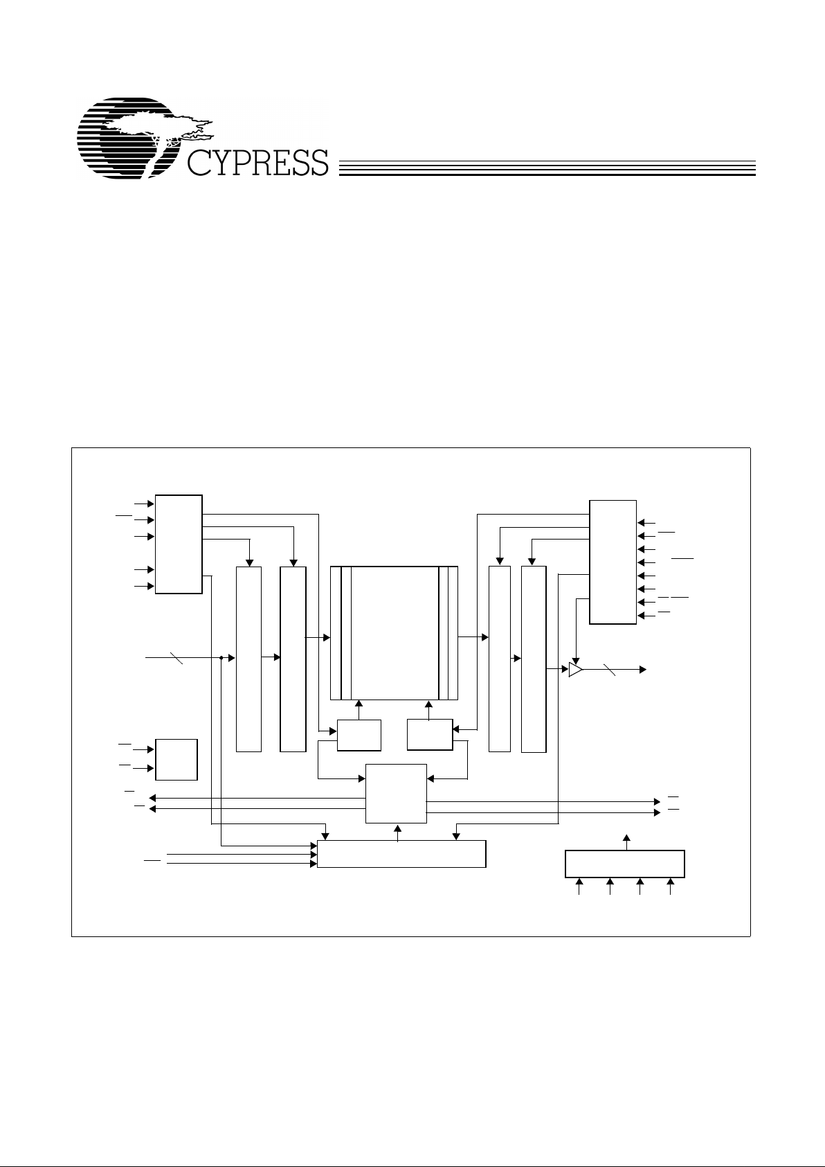
Prelimi n ary Top Level Block Diagram
Port A
Control
Logic
Port B
Control
Logic
Bus Matching Input Register
Bus Matching Output Register
Dual Ported
Status
Flag Logic
Programmable Flag Offset Registers
4K/16K/64Kx80
FIFO
CLKA
CSA
ENA
MR
PR
FF/IR
AF
FS0/SD
FS1/SEN
A
79–0
B
79–0
CLKB
CSB
ENB
BE/FWFT
SIZE1B
SIZE2B
EF/OR
AE
Read Data Path Logic
80
80
Reset
Logic
SIZE1A
SIZE2A
Write Data Path Logic
RT/SPM
JTAG Controller
TDI TCK TMS TRST
TDO
OE
Read
PointerPointer
Write
Memory
For the most recent information, visi t th e Cypress web site at www.cypress.com

CY7C4808V25
CY7C4806V25
CY7C4804V25PRELIMINARY
2
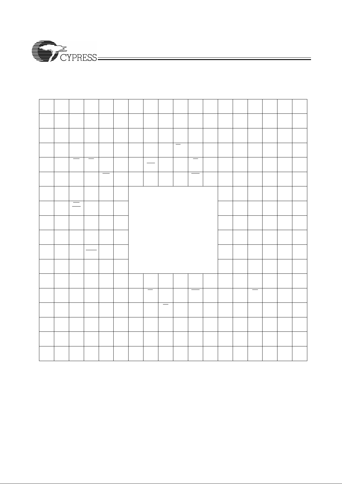
Pin Configuration for CY7C4804V25 (Top Vie w )
1 2 3 4 5 6 7 8 9 10 11 12 13 14 15 16 17 18
AV
DDQVDDQ
A16 A19 V
DDQ
A30 A34 GND CLKA A42 GND A48 A51 V
DDQ
A55 A57 V
DDQVDDQ
A
BV
DDQ
A10 A14 A17 V
DDQ
A29 A33 GND A39 A41 GND A45 A50 V
DDQ
A54 A56 A58 V
DDQ
B
CA9 A8 V
DDQ
A13 A18 A28 A32 A36 A38 V
DDQ
A44 A46 A49 A52 A53 V
DDQ
A59 A60 C
DA7 A6 A11V
DDQ
A20 GND A27 SH GND FF/IR VDD A43 GND A47 V
DDQ
A63 A67 A69 D
EV
DDQVDDQ
MR PR VDDA25 GND FS1/
SEN
GND GND AF GND GND VDD TDI A66 V
DDQVDDQ
E
FA12A15SIZE1AGND A21 A24 A31 A35 A37 ENA CSA A40 A61 VDD GND A64 A65 A68 F
GA5 A2SIZE2BFS0/
SD
GND A23 A62 GND TDO A70 A71 A72 G
HGNDGNDRT/
SPM
V
DD
SIZE 1BA4 A73 A74 TCK A75 GND GND H
JB2 B3V
DDQ
A1 GND A0 A76 GND GND A77 A78 A79 J
K B6 B7 B4 GND GND A3 B76 GND B77 V
DDQ
B78 B79 K
L GND GND B5 BE/
FWFT
A22 A26 B73 B74 TMS B75 GND GND L
M B10 B9 VREF B8 GND SIZE
2A
B69 GND TRST B70 B71 B72 M
N B14 B13 B12 GND B1 B11 B31 B35 B37 B40 B43 B45 B65 NC GND B66 B67 B68 N
PV
DDQVDDQ
B15 NC NC B0 GND EF/
OR
GND GND CSB GND NC VDD OE B64 V
DDQVDDQ
P
RB18 B17B16V
DDQ
NC GND NC VDD AE GND ZQ ENB GND NC V
DDQ
B61 B62 B63 R
TB20 B19 V
DDQ
B24 B27 B28 B32 B36 V
DDQ
B41B44B46B49 B52B53V
DDQ
B59 B60 T
UV
DDQ
B21 B22 B25 V
DDQ
B29 B33 GND B38 B42 GND B47 B50 V
DDQ
B54 B56 B58 V
DDQ
U
VV
DDQVDDQ
B23 B26 V
DDQ
B30 B34 GND B39 CLKB GND B48 B51 V
DDQ
B55 B57 V
DDQVDDQ
V
1 2 3 4 5 6 7 8 9 10 11 12 13 14 15 16 17 18
CY7C4808V25
CY7C4806V25
CY7C4804V25PRELIMINARY
3
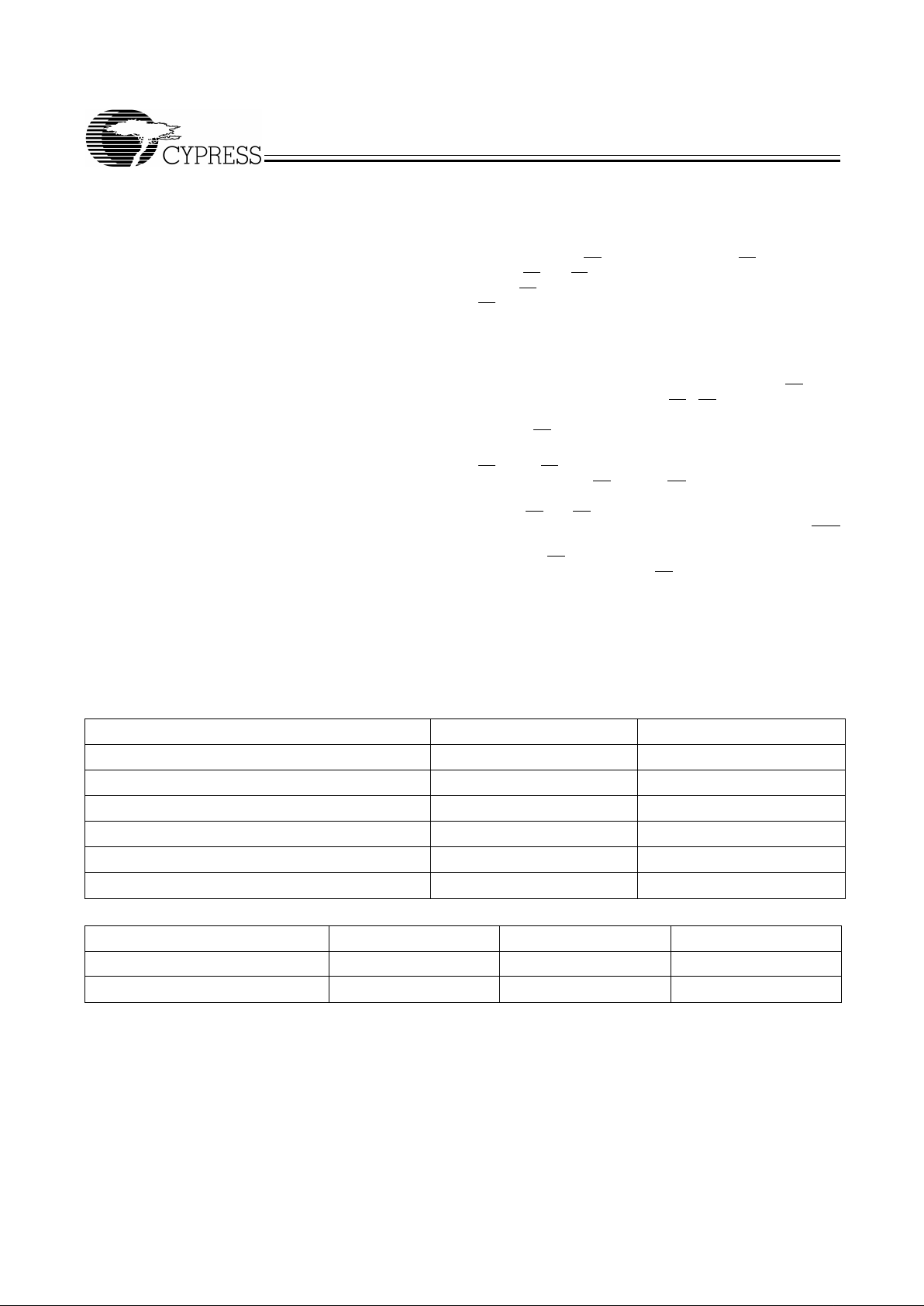
Pin Configuration for CY7C4806V25 (Top View)
1 2 3 4 5 6 7 8 9 10 11 12 13 14 15 16 17 18
AV
DDQVDDQ
A16 A19 V
DDQ
A30 A34 GND CLKA A42 GND A48 A51 V
DDQ
A55 A57 V
DDQVDDQ
A
BV
DDQ
A10 A14 A17 V
DDQ
A29 A33 GND A39 A41 GND A45 A50 V
DDQ
A54 A56 A58 V
DDQ
B
CA9 A8 V
DDQ
A13 A18 A28 A32 A36 A38 V
DDQ
A44 A46 A49 A52 A53 V
DDQ
A59 A60 C
DA7 A6 A11V
DDQ
A20 GND A27 SH GND FF/IR VDD A43 GND A47 V
DDQ
A63 A67 A69 D
EV
DDQVDDQ
MR PR VDDA25 GND FS1/
SEN
GND GND AF GND VDD VDD TDI A66 V
DDQVDDQ
E
FA12A15SIZE1AGND A21 A24 A31 A35 A37 ENA CSA A40 A61 VDD GND A64 A65 A68 F
GA5 A2SIZE2BFS0/
SD
GND A23 A62 GND TDO A70 A71 A72 G
HGNDGNDRT/
SPM
V
DD
SIZE 1BA4 A73 A74 TCK A75 GND GND H
JB2 B3V
DDQ
A1 GND A0 A76 GND GND A77 A78 A79 J
K B6 B7 B4 GND GND A3 B76 GND B77 V
DDQ
B78 B79 K
L GND GND B5 BE/
FWFT
A22 A26 B73 B74 TMS B75 GND GND L
M B10 B9 VREF B8 GND SIZE
2A
B69 GND TRST B70 B71 B72 M
N B14 B13 B12 GND B1 B11 B31 B35 B37 B40 B43 B45 B65 NC GND B66 B67 B68 N
PV
DDQVDDQ
B15 NC NC B0 GND EF/
OR
GND GND CSB GND NC VDD OE B64 V
DDQVDDQ
P
RB18 B17B16V
DDQ
NC GND NC VDD AE GND ZQ ENB GND NC V
DDQ
B61 B62 B63 R
TB20 B19 V
DDQ
B24 B27 B28 B32 B36 V
DDQ
B41B44B46B49 B52B53V
DDQ
B59 B60 T
UV
DDQ
B21 B22 B25 V
DDQ
B29 B33 GND B38 B42 GND B47 B50 V
DDQ
B54 B56 B58 V
DDQ
U
VV
DDQVDDQ
B23 B26 V
DDQ
B30 B34 GND B39 CLKB GND B48 B51 V
DDQ
B55 B57 V
DDQVDDQ
V
1 2 3 4 5 6 7 8 9 10 11 12 13 14 15 16 17 18

CY7C4808V25
CY7C4806V25
CY7C4804V25PRELIMINARY
4
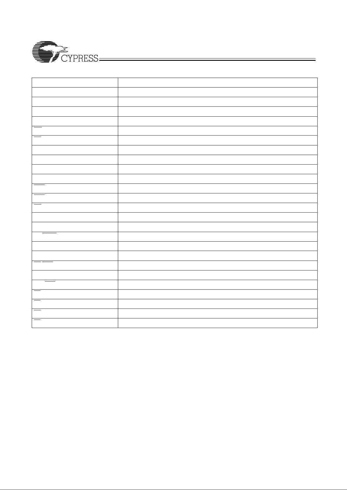
Pin Configuration for CY7C4808V25 (Top View)
1 2 3 4 5 6 7 8 9 10 11 12 13 14 15 16 17 18
AV
DDQVDDQ
A16 A19 V
DDQ
A30 A34 GND CLKA A42 GND A48 A51 V
DDQ
A55 A57 V
DDQVDDQ
A
BV
DDQ
A10 A14 A17 V
DDQ
A29 A33 GND A39 A41 GND A45 A50 V
DDQ
A54 A56 A58 V
DDQ
B
CA9 A8 V
DDQ
A13 A18 A28 A32 A36 A38 V
DDQ
A44 A46 A49 A52 A53 V
DDQ
A59 A60 C
DA7 A6 A11V
DDQ
A20 GND A27 SH GND FF/IR VDD A43 GND A47 V
DDQ
A63 A67 A69 D
EV
DDQVDDQ
MR PR VDDA25 GND FS1/
SEN
GND GND AF GND GND VDD TDI A66 V
DDQVDDQ
E
FA12A15SIZE1AGND A21 A24 A31 A35 A37 ENA CSA A40 A61 GND GND A64 A65 A68 F
GA5 A2SIZE2BFS0/
SD
GND A23 A62 GND TDO A70 A71 A72 G
HGNDGNDRT/
SPM
V
DD
SIZE 1BA4 A73 A74 TCK A75 GND GND H
JB2 B3V
DDQ
A1 GND A0 A76 GND GND A77 A78 A79 J
K B6 B7 B4 GND GND A3 B76 GND B77 V
DDQ
B78 B79 K
L GND GND B5 BE/
FWFT
A22 A26 B73 B74 TMS B75 GND GND L
M B10 B9 VREF B8 GND SIZE
2A
B69 GND TRST B70 B71 B72 M
N B14 B13 B12 GND B1 B11 B31 B35 B37 B40 B43 B45 B65 NC GND B66 B67 B68 N
PV
DDQVDDQ
B15 NC NC B0 GND EF/
OR
GND GND CSB GND NC VDD OE B64 V
DDQVDDQ
P
RB18 B17B16V
DDQ
NC GND NC VDD AE GND ZQ ENB GND NC V
DDQ
B61 B62 B63 R
TB20 B19 V
DDQ
B24 B27 B28 B32 B36 V
DDQ
B41B44B46B49 B52B53V
DDQ
B59 B60 T
UV
DDQ
B21 B22 B25 V
DDQ
B29 B33 GND B38 B42 GND B47 B50 V
DDQ
B54 B56 B58 V
DDQ
U
VV
DDQVDDQ
B23 B26 V
DDQ
B30 B34 GND B39 CLKB GND B48 B51 V
DDQ
B55 B57 V
DDQVDDQ
V
1 2 3 4 5 6 7 8 9 10 11 12 13 14 15 16 17 18
CY7C4808V25
CY7C4806V25
CY7C4804V25PRELIMINARY
5
Functional Description
The CY7C480XV25 family of FIFOs is comprised of
high-speed, low-power, CMOS Synchronous (clocked) FIFO
memories, meaning both independent ports employ a synchronous interface. All data transfers through a port are gated
to the LOW -t o-HIGH tra nsition of the cloc k on ei ther port by t he
enable signa l. The cloc ks fo r each port are independen t of one
another and can be asynchronous or coincident. The enable
for each port is arranged to provide a simple unidirectional
interface between microprocessors and/or buses with synchronous control.
T w o kinds of reset are av ailabl e on the CY7C480XV25: Master
Reset and Partial Reset. Mas ter Reset ini tiali z es the read and
write pointers to the first location of the memory array, configures the FIFO for Big Endian or Little Endian byte arrangement, selects the CY standard or First-Word Fall-Through
(FWFT) mode, and determines the configuration of the programmabl e flags . The f lags can b e prog rammed eit her in s erial
mode or in parallel mode. The FIFO also comes with three
possible default flag offset settings: 8, 16, or 64.
Partial Reset also sets the read and write pointers to the first
location of the memory. Unlike Master Reset, any settings existing prior to Pa rtial Reset (i .e., pr ogrammi ng method and partial flag default offsets) are retained. Partial Reset is useful
since it p ermits flus hing of the FIFO memory without changi ng
any configuration settings.
The CY7C480XV25 have two modes of operation: CY Standard Mode or First-Word Fall-Through Mode (FWFT). In the
CY Standard Mode, the first word written to an empty FIFO is
deposited into the memory array. A read operation is required
to access that word (along with all other subsequent words
residing in m emory). In the FWFT Mode, the first w ord written
to an empty FIFO appears automatically on the outputs, and
no read ope ra tion is r equir ed. Ne v ertheless , ac cess ing su bsequent words does necessitate formal read request. FWFT
mode is primarily used for cascading multiple FIFOs.
The FIFO has an EF
/OR flag on port B and FF/IR flag on Port
A. The EF
and FF functions are selected in the CY Standard
Mode. EF
indicates whether or not the FIFO memory is empty .
FF
shows whether or not the memory is full. The IR and OR
functions are select ed in the Fir st-W ord F all-Thr ough mode . IR
indicates whether or not the FIFO has memory locations av ai lable. OR sho ws whet her th e FIFO has data available f or r eading or not. It marks the presence of valid data on the outputs.
The FIFO has a programmable Almost Empty f lag (AE
) and a
programma ble Almost Full f lag (AF
). AE indicates the number
of words left in the FIFO memory is at the user-defined
amount. AF
indicates the number of words written into the
FIFO memory has achieved a predetermined amount.
FF
/IR and AF flags a re synchroni zed to port A cloc k tha t writes
data into its array. EF
/OR and AE flags are synchronized to
Port B clock that reads data from its array. Programmable offsets for AE
and AF are loaded in parall el via P ort A or in serial
via the SD input. The Serial Programming Mode pin (SPM
)
makes this sel ection. Three def ault offsets sett ing are also provided. The AE
threshold can be set at 8, 16, or 64 locations
from the empty boundary and AF
threshold ca n be set at 8, 16,
or 64 locations from the full boundary. All these choices are
made using the FS0 and FS1 inputs during Master Reset.
The CY7C480XV25 FIFOs are characterized for operation
from 0°C to 70°C commercial, and from –40°C to 8 5°C in dustrial.
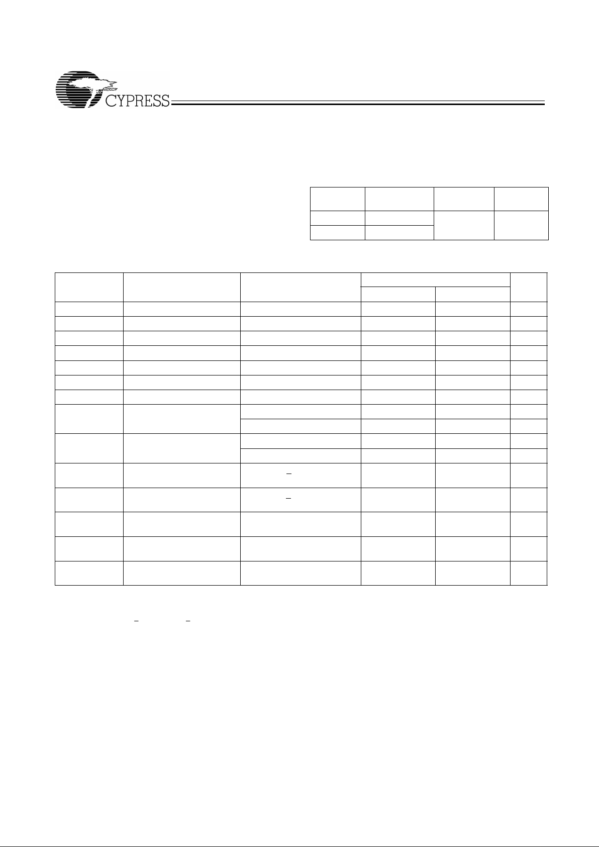
Selection Guide
CY7C480XV25-200 CY7C480XV25-166
Maximum Frequency (MHz) 200 166
Maximum Access Time (ns) 3.3 3.7
Minimum Cycle Time (ns) 5 6
Minimum Data or Enabl e Set-Up (ns) 0.9 0.9
Minimum Data or Enable Hold (ns) 0.6 0.6
Maximum Flag Delay (ns) 3.3 3.7
CY7C4808V25 CY7C4806V25 CY7C4804V25
Density 64K x 80 16K x 80 4K x 80
Pac kage 288 FBGA 288 FBGA 288 FBGA
CY7C4808V25
CY7C4806V25
CY7C4804V25PRELIMINARY
6
Pin Description
Pin Description
V
DDQ
Po wer supply for I/Os
V
DD
Po wer supply for internal logic
GND Ground
V
REF
Reference voltage
MR
Master reset
PR
Partial reset
A
0–A79
Input data bus
B
0–B79
Outp u t da ta bus
ENA Port A enable pin
ENB Port B enable pin
CSA
Port A chip select
CSB
Port B chip select
OE
Output enable
CLKA Port A clock
CLKB Port B clock
BE/FWFT
Big/Little Endian and CY Standard/First-Word Fall-Through mode select pin
SIZE1A, SIZE2A Port A bus siz e configuration pins
SIZE1B, SIZE2B Port B bus siz e configuration pins
RT
/SPM Retransmit pin/serial programming select
TDI, TDO, TCK, TMS , TRST JTAG pins
FS1/SEN
, FS0/SD Programmable flags configuration pins
EF
/OR Empty/Output Ready flag (Port B)
FF
/IR Full/Input Ready flag (Por t A)
AE
Programmable Almost Empty flag (P ort B)
AF
Programmable Almost Full flag (Port A)
CY7C4808V25
CY7C4806V25
CY7C4804V25PRELIMINARY
7
Maximum R atings
(Above which the useful life may be impaired. For user guidelines, not tested.)
Storage Temperature .............. .. .. ........... .. ....–65
°
C to +150°C
Ambient Temperature with
Power Applied ....... ... .. ............... .. ... .............. . –55
°
C to +125°C
Supply Voltage to Ground Potential ...............–0.5 V to +3 .6 V
DC Vo lt age Applied to Outputs
in High Z State
[1]
................................... –0.5V to V
DDQ
+0.5V
DC Input Voltage
[1]
................................ –0.5V to V
DDQ
+0.5V
Current into Outputs (LOW)......................................... 20 mA
Static Discharge Voltage ...........................................>2001V
(per MIL-STD-883, Method 3015)
Latch-Up Current.....................................................>200 mA
Notes:
1. Minimum voltage equal –2.0V for pulse duration less than 20ns.
2. All voltage referenced to ground.
3. Overshoot: V
IH
(AC) < VDD+1.5V for t < t
clk
/2, Power-Up: VIH<2.6V and VDD<2.4V and V
DDQ
<1.4V for t<200 ns.
Operating Range
Range
Ambient
Temperature
V
DD
V
DDQ
Commercial 0°C to +7 0°C 2.5V ± 100 mV 1.4V to 1.9V
Industrial –40°C to +85°C
DC Specifications
(All I/Os e xcept JTAG ports will be at HSTL level)
[2, 3]
CY7C480XV25
Parameter Description Test Co ndit ions Min. Max. Unit
V
DD
Power Supply Voltage 2.4 2.6 V
V
DDQ
I/O Supply Voltage 1.4 1.9 V
V
REF
Input Reference Voltage Typical value = 0.75V 0.68 1.0 V
V
OH
Outp ut HIGH Voltage (V
DDQ
/2) + 0.3 V
DDQ
V
V
OL
Output LOW Voltage V
SS
(V
DDQ
/2) – 0.3 V
V
IH
Input HIGH V o ltage V
REF
+ 0.1 (V
DDQ
/2) + 0.3 V
V
IL
Input LOW Voltage –0.3 V
REF
– 0.1 V
V
OH_JTA G
JTAG Port Output
High Voltage
I
OH
= –100 µA 2.1 V
I
OH
= –2 mA 1.7 V
V
OL_JTA G
JTAG Port Output
Low V oltage
IOL= 100 µA 0.2 V
IOL= 2 mA 0.7 V
V
IH_JTA G
JTAG Port Input
High Voltage
V
OUT>VVOH
(min.) 1.7 VDD+0.3 V
V
IL_JTA G
JTAG Port Input
Low V oltage
V
OUT<VVOL
(max.) –0.3 0.7 V
I
IX
Input Leakage
Current
–10 +10
µA
I
OZL,IOZH
Outp ut OFF,
High Z Current
–10 +10
µA
I
SB
Average Standby
Current
10 mA
CY7C4808V25
CY7C4806V25
CY7C4804V25PRELIMINARY
8
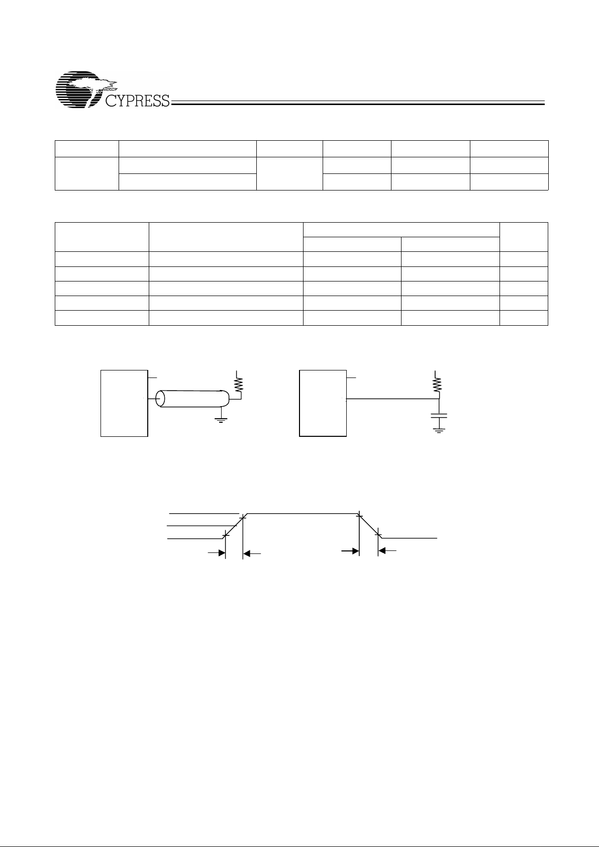
AC Test Loads and Waveforms
Notes:
4. Both clocks switching at maximum speeds, data switching at half the clock frequency.
5. Unless otherwise noted, test conditions assume signal transition time of 2 V/ns, timing reference levels of 0.75V , V
ref
= 0.75V, RQ = 250Ω, V
DDQ
= 1.5V, input
pulse levels of 0.25V to 1.25V, and output loading of the specified I
OL/IOH
and load capacitance shown in (b) of AC test loads.
DC Specifications
(continued)
[4]
Parameter Description Conditions 200 MHz 166 MHz Unit
I
CC
Operating current (Typical) VDD = max.,
I
OUT =
0 mA
225 185 mA
Operating current (Max.) 300 250 mA
AC Spe cificati ons
(A 50Ω load terminated into 0. 75V is used wit h V
DDQ
)
CY7C480XV25
Parameter Description Min. Max. Unit
F
MAX
Max. Frequency 200 MHz
t
CYC
Clock Cycle Time 5 ns
t
SD
Input Data Set-Up Time 0.9 ns
t
HD
Input Data Hold Time 0.6 ns
t
A
Access Time 3.3 ns
V
REF
(V
DDQ
)/2
Output
Device
Under
Test
Z
O
= 50
Ω
R
L
= 50
Ω
V
TH
= (V
DDQ
)/2
RL = 50
Ω
V
REF
(
V
DDQ
)/2
O
utput
D
evice
U
nder
T
est
V
TH
= (V
DDQ
)/2
5
pF
ALL INPUT PULSES
0.75V
1.25V
0.25V
10%
90%
t
R
tF9
0%
1
0%
t
R
≤ 0.5 ns, tF ≤ 0.5 ns
[5]
(a) Test Loads
(b) Test Loads
CY7C4808V25
CY7C4806V25
CY7C4804V25PRELIMINARY
9
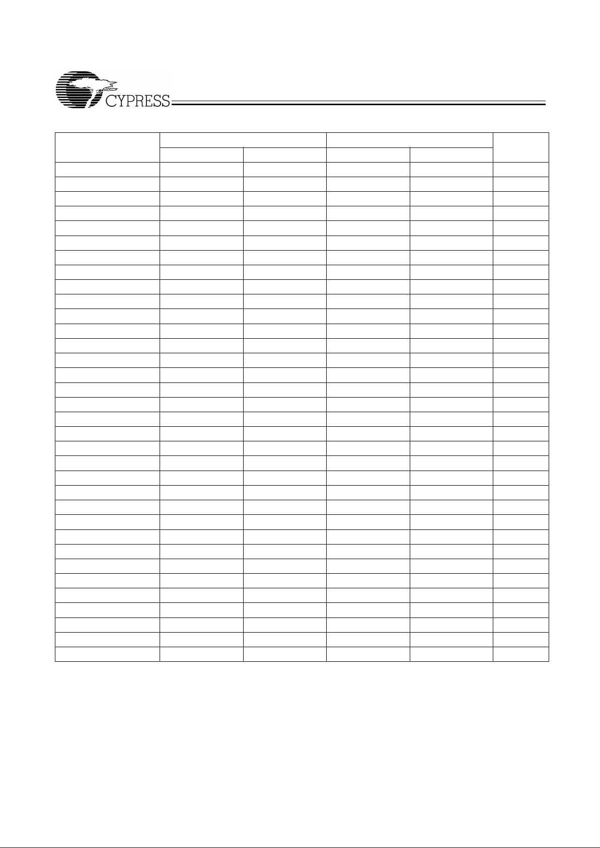
Timing Parameters
7C480XV25-200 7C480XV25-166
Parameter Min. Max. Min. Max. Unit
f
S
200 166 MHz
t
CLK
5 6 ns
t
CLKH
2.5 3 ns
t
CLKL
2.5 3 ns
t
DS
0.9 0.9 ns
t
ENS
0.9 0.9 ns
t
RSTS
2 2 ns
t
FSS
2 2 ns
t
BES
2 2 ns
t
SMPS
2 2 ns
t
SDS
0.9 0.9 ns
t
SENS
0.9 0.9 ns
t
FWS
0.9 0.9 ns
t
DH
0.6 0.6 ns
t
ENH
0.6 0.6 ns
t
RSTH
2 2 ns
t
FSH
2 2 ns
t
BEH
2 2 ns
t
SPMH
2 2 ns
t
SDH
0.6 0.6 ns
t
SENH
0.6 0.6 ns
t
SPH
0.6 0.6 ns
t
SKEW1
8 10 ns
t
SKEW2
8 10 ns
t
A
3.3 3.7 ns
t
WFF
3.3 3.7 ns
t
REF
3.3 3.7 ns
t
PAE
3.3 3.7 ns
t
PAF
3.3 3.7 ns
t
RSF
4 4 ns
t
EN
3.5 3.5 ns
t
DIS
3.5 3.5 ns
t
PRT
25 25 ns
t
RTR
45 45 ns
 Loading...