

Cypress Semiconductor CY7C43686AV-7AC, CY7C43686AV-15AC, CY7C43686AV-10AC, CY7C43646AV-7AC, CY7C43646AV-15AC Datasheet
...
V
CY7C43646AV
PRELIMINARY
3.3 V 1K/4K/16K x36/x18x2 Tri Bus FIFO
Features
• 3.3V high-speed, low-power, first-in first-out (FIFO)
memories w/ three in dependent ports (one bidirectional
x36, and two unidir ectional x18)
• 1K x36/x18x2 (CY7C43646AV)
• 4K x36/x18x2 (CY7C43666AV)
• 16K x36/x18x2 ( CY7C43686AV)
• 0.25-micron CMOS for optimum speed/pow er
• High-speed 133- MHz operat ion (7.5- ns read/wri te cy cle
times)
• Low po w er
= 60 mA
—I
CC
= 12 mA
—I
SB
• Fully asynchronous and simultaneous read and write
operation permitted
• Mailbox bypass register for each FIFO
• Parallel and Serial Programmable Almost Full and
Almost Empty flags
• Retransmit function
• Standard or FW FT mode user sel ectable
• Partial Reset
• Big or Little Endian f ormat for word or byte bus sizes
• 128-pin TQFP packaging
• 3.3V pin-compatible, feature enhanced, density upgrade to IDT723626/36/46 family
• Easily expandable in width and depth
CY7C43666AV/CY7C43686AV
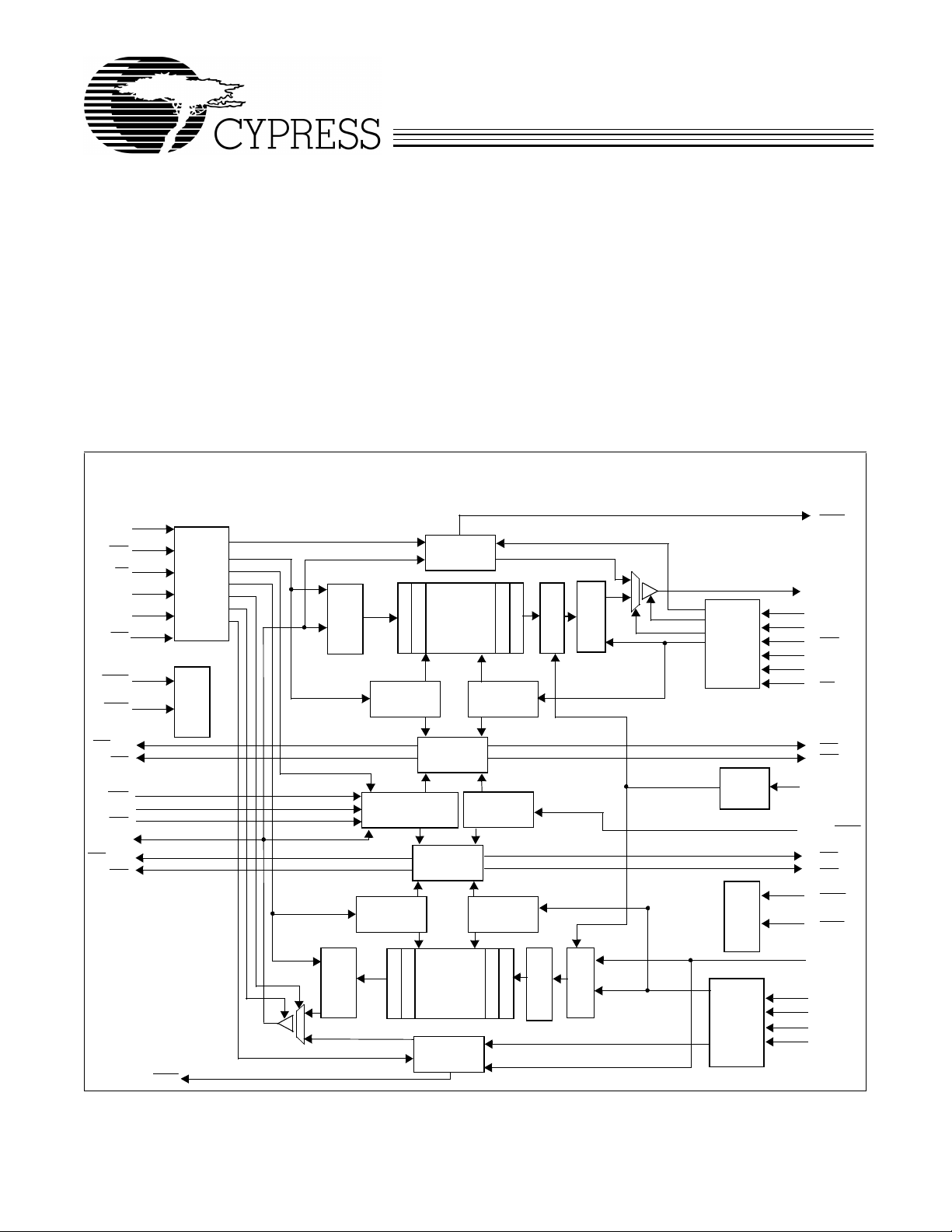
Logic Block Diagram
CLKA
CSA
W/RA
ENA
MBA
RT2
MRS1
PRS1
FFA/IRA
AFA
SPM
FS0/SD
FS1/SEN
A
0–35
EFA/ORA
AEA
MBF2
Por t A
Control
Logic
FIFO1,
Mail1
Reset
Logic
Input
Register
Programmable
Flag Offset
Registers
Output
Register
Write
Pointer
Read
Pointer
Mail1
Register
1K/4K/16K
x36
Dual Ported
Memory
Status
Flag Logic
Status
Flag Logic
1K/4K/16K
x36
Dual Ported
Memory
Mail2
Register
Read
Pointer
Timing
Mode
Write
Pointer
Input
Bus Matching
MBF1
B
0–17
CLKB
Output
Output
Register
Bus Matching
Input
Register
Port B
Control
Logic
Common
Port Logic
(B and C)
FIFO2,
Mail2
Reset
Logic
Port C
Control
Logic
RENB
CSB
SIZEB
MBB
RTI
EFB/ORB
AEB
BE
BE/FWFT
FFC/IRC
AFC
MRS2
PRS2
C
0–17
CLKC
WENC
SIZEC
MBC
Cypress Semiconductor Corporation
• 3901 North First Street • San Jose • CA 95134 • 408-943-2600
September 3, 1999
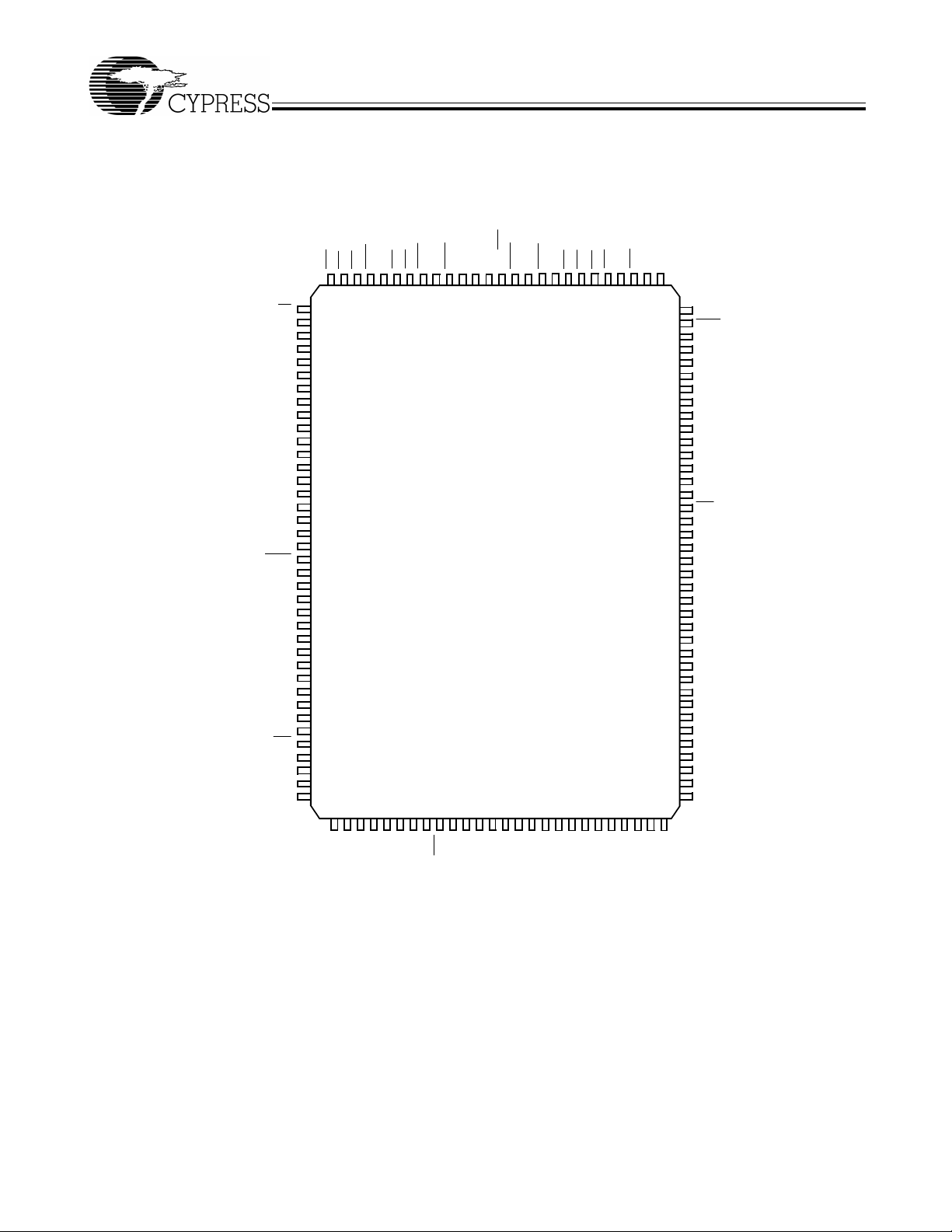
Pin Configuration
W/RA
ENA
CLKA
GND
A
A
A
A
V
A
A
GND
A
A
A
A
A
A
A
BE/FWFT
GND
A
V
A
A
A
A
GND
A
A
A
A
A
RT2
A
GND
A
A
CY7C43646AV
PRELIMINARY
TQFP
Top View
MBF2
AEA
AFA
VCCPRS1
EFA/ORA
FFA/IRA
CSA
128
127
126
125
124
123
1
2
3
122
4
5
35
6
34
33
7
32
8
9
CC
10
31
11
30
12
29
13
14
28
15
27
26
16
25
17
24
18
19
23
20
21
22
22
CC
23
21
24
20
25
19
26
18
27
28
17
29
16
30
15
31
14
32
13
33
34
12
35
36
11
37
10
38
39404142434445464748495051525354555657585960616263
5
6A7A8A9
A
GND
FS0/SD
FS1/SEN
GND
CLKC
MRS1
MBA
121
120
119
118
117
116
115
CY7C43646AV
CY7C43666AV
CY7C43686AV
2
0A1
A
A
A3A4A
CC
V
SPM
GND
CY7C43666AV/CY7C43686AV
GND
FFC/IRC
MRS2
114
B
AFC
AEB
VCCMBF1
MBB
113
112
111
110
109
0
5B4B3B2B1
B
EFB/ORB
108
CSB
RENB
WENC
107
106
105
104
103
102
CLKB
101
PRS2
V
100
CC
99
C
17
98
C
16
97
C
15
96
C
14
GND
95
MBC
94
93
C
13
92
C
12
91
C
11
90
C
10
89
C
9
88
C
8
RT1
87
86
C
7
C
85
6
SIZEB
84
83
GND
82
C
5
81
C
4
80
C
3
C
79
2
C
78
1
77
C
0
76
GND
B
75
17
74
B
16
SIZEC
73
V
72
CC
B
71
15
B
14
70
B
69
13
B
68
12
GND
67
B
66
11
B
65
10
64
7
6
B
GND
B9B8B
CC
V
2
PRELIMINARY
CY7C43646AV
CY7C43666AV/CY7C43686AV
Functional Description
The CY7C436X6AV is a monolithic, high-speed, low-power,
CMOS Bidirectional Synchronous (clocked) FIFO memory
which supports cloc k freque ncies up to 133 M Hz an d h as read
access times as fast as 6 ns. Two independent
256/512/1K/4K/16K x 36 dual-port SRAM FIFOs on board
each chip b uf fe r d ata i n opposi te di rec tions . FI FO data o n Port
B can be input and output in 36-bit, 18-b it, or 9-bit format s with
a choice of Big or Little Endi an configurations.
The CY7C436X6AV is a synchronous (clocked) FIFO, meaning each port emplo ys a sync hron ous int erf ace . All data t ransfers th rough a port are gate d to the LO W - to-HI GH trans iti on of
a port clock by enable signals. The clocks for each port are
independent of one another and can be asynchronous or coincident. The enables for each port are arranged to provide a
simple bidi rectional i nterfac e between microproces sors and/or
buses with synchronous control.
Communication b etw een each port ma y b ypas s the FIF Os via
two mailbox registers. The mailbox registers’ width matches
the selected P ort B bus width. Each mailbo x register has a f lag
(MBF1
and MBF2) to signal when new mail has been stored.
T w o kinds of reset are a vailab le on th e CY7C436X6A V : Master
Reset and Partial Reset . Master Rese t init ializ es t he read and
write pointers to the fi rst location of the memory array, configures the FIFO for Big or Little Endian byte arrangement and
selects serial flag programming, parallel flag programming, or
one of the three possible defaul t flag offset settings, 8, 16, or
64. Each FIFO has its own independent Master Reset pin,
MRS1
and MRS2.
Partial Reset also sets the read and write pointers to the first
location of the memory. Unlike Master Reset, any settings existing prior to P artial Reset ( i.e., progr amming meth od and partial flag default offsets) are retained. Par tial Reset is useful
since it permits fl ushing of the FI FO memory witho ut chang in g
any configuration settings. Each FIFO has its own independent Partial Reset pin, PRS1
The CY7C436X6AV have two modes of operation: In the CY
Standard Mode, the first word written to an em pty FIFO is deposited into the memory array. A read operation is requi red to
access that word (along with all other words residing in memory). In the Fi rst-Word Fall-Through Mode (FWFT ), the fi rst
long-word (3 6-bit wide) written to an empty FIFO appears au-
and PRS2.
tomatically on the out puts, no read operation required (nevertheless, accessing subsequent words does necessitate a formal read request). The state of the FWFT
FIFO operation determines the mode in use.
Each FIFO has a combined Empty/Output Ready Flag
(EFA
/ORA and EFB/ORB) and a combined Full/Input Ready
Flag (FFA
selected in the CY Standard Mode. EF
memory is full or not. The IR and OR funct ions are se lected in
the First Word Fal l Throu gh Mode. IR indic ates wheth er or not
the FIFO has available memory locations. OR shows whether
the FIFO has data available for reading or not. It marks the
presence of val id data on the outputs.
Each FIFO has a programmable Almost Empty flag (AEA
AEB
AEA
ten to FIFO memory achieve a predetermined “almost empty
state.” AFA
words written t o the m emory achi ev e a predet ermined “almost
full sta te.”
IRA, IRC, AFA
that writes data into its array. ORA, ORB, AEA
synchronized to the port clock that reads data from its array.
Programmable offset for AEA
in parallel using Port A or in serial via the SD input. Three
default offset settings are also provided. The AEA
threshold can be set at 8, 16, or 64 locations from the empty
boundary and AFA
64 locations from the full boundary. All these ch oices are made
using the FS0 and FS1 inputs during Master Reset.
Two or more devices may be used in parallel to create wider
data paths. Such a width expansion requires no additio nal external components.
If at any time the FIFO is not actively performing a function,
the chip will automatically power down. During the Power
Down state, supply cur rent cons umption (I
Initiating an y oper ation ( by ac tiv at ing c ontrol inp uts) will imme diately take the device out of the Power Down state.
The CY7C436X6AV are characterized for operation from 0
to 70°C. I nput ESD prot ection is g reater t han 2001V, and la tchup is prevented by the use of guard rings.
/IRA and FFC/IRC). The EF and FF functions are
) and a programmable Almost Full flag (AFA and AFC).
and AEB indicate when a selected number of words writ-
and AFC indicate when a selected number of
, and AFC are synchronized to the port clock
, AEB, AF A, and AF C are loa ded
and AFC threshold can be set at 8, 16, or
/STAN pin during
indicates whether the
and
, and AEB are
and AEB
) is at a minimum.
CC
°
C
Selection Guide
7C43646/66/86AV-7 7C43646/66/86AV-10 7C43646/66/86AV-15
Maximum Frequency (MHz) 133 100 66.7
Maximum Access Time (ns) 6 8 10
Minimum Cycle Time (ns) 7.5 10 15
Minimum Data or Enable Set-Up (ns) 3 4 5
Minimum Data or Enable Hold (ns) 0 0 0
Maximum Flag Delay (ns) 6 8 10
Active Power Supply
Current (I
Density 1K x 36/x18x2 4K x 36/18x2 16K x 36/x18x2
Package 128 TQFP 128 TQFP 128 TQFP
CC1
) (mA)
Commercial 60 60 60
Industrial 60
7C43646AV 7C43666AV 7C43686AV
3

CY7C43646AV
PRELIMINARY
Pin Definitions
Signal Name Description I/O Function
A
0–35
AEA
AEB
AFA
AFC
B
0–17
BE/FWFT
C
0–17
CLKA Port A Clock I CLKA is a c ontinuous clock t hat synchr onizes all data tr ansfer s through P ort A and can
CLKB Port B Clock I CLKB is a c ontinuous clock t hat synchr onizes all data tr ansfer s through P ort B and can
CLKC P ort C Clock I CLKC is a contin uous cloc k that synchroniz es all data tr ansfe rs throu gh P ort C and can
CSA
CSB
EFA
/ORA Port A Empty/
/ORB Port B Empty/
EFB
ENA Port A Enable I ENA must be HIGH to enable a L O W -to- HIGH tra nsition of CLKA to rea d or write dat a
ENB Port B Enable I ENB must be HIGH to enable a L O W -to- HIGH tra nsition of CLKB to rea d or write dat a
Port A Data I/O 36-bit bidirectional data port for side A.
Port A Almost
Empty Flag
Port B Almost
Empty Flag
Port A Almost
Full Flag
Port C Almost
Full Flag
Port B Data O 18-bit output data port for port B.
Big Endi-
an/First-Word
Fall-Through
Select
Port B Data I 18-bit input data port for port C.
Port A Chip
Select
Port B Chip
Select
Output Ready
Flag
Output Ready
Flag
O Programmab le Almost Empty flag sy nchroni z ed to CLKA. It is LO W when the nu mber
of words in FIFO2 is less t han or equa l to the val ue in the Alm ost Empty A of fset register ,
X2.
O Programmab le Almost Empty flag sync hro nize d to CLKB. It is LOW when the nu mber
of words in FIFO1 is less t han or equa l to the val ue in the Alm ost Empty B of fset register ,
X1.
O Programmable Almost Full flag synchroniz ed to CLKA. It is LOW when the n umber of
empty locations in FIFO1 is less than or equal to the value in the Almost Full A offset
register, Y1.
O Programmab le Almost Ful l flag synchron ized to CLKC. It is LOW when the number of
empty locations in FIFO2 is less than or equal to the value in the Almost Full B offset
register, Y2.
I This is a dual-purpose pin. During Maste r Reset, a HIGH on BE will selec t Big Endian
operation. In thi s case, depe nding on the bus size, the most signi ficant byt e or word on
Port A is read fr om Port B first (A- to- B data flow) or written to Port C first ( C-to-A data
flow). A LO W on BE will select Little Endia n operati on. In this case , the lea st significant
byte or word on Port A is read from Port B first (for A-to-B data flow) or written to Port
C first (C-to-A data flow). After Master Reset, this pin selects the timing mod e. A HIGH
on FWFT
Once the timing mode has be en selecte d, the le ve l on FWFT
device operation.
be asynchronous or coincident to CLKB. FFA
synchronized t o the LOW-to-HIGH transition of CLKA.
be asynchronous or coincident to CLKA. EFB
the LOW-to-HIGH transition of CLKB.
be asynchronous or coinciden t to CLKA. FFC
LOW-t o-HIGH transition of CLKC.
ICSA must be LOW to enable a LOW-to HIGH trans it ion of CLKA to read or write on
Port A. The A
ICSB must be LOW to enable a LOW-to HIGH trans it ion of CLKB to read or write on
Port B. The B
O This is a dual -functi on pin. In the CY S tandard Mode , the EF A f unction is selected. EF A
indicates whether or not the FIFO2 memo ry is empty. In the FWFT mode, the ORA
function is selected. ORA indicates the presence of valid data on A
able for reading. EFA
O This is a dual-funct ion pin. In the CY Standard Mode, the EFB funct ion is selected. EFB
indicates whether or not the FIFO1 memo ry is empty. In the FWFT mode, the ORB
function is selected. ORB indicates the presence of valid data on B
able for reading. EFB
on Port A.
on Port B.
selects CY Standard Mode , a LOW selects First-Word Fall-Through Mode.
outputs are in the high-impedance state when CSA is HIGH.
0–35
outputs are in the high- impedance state when CSB is HIGH.
0–17
/ORA is synchronized to t he LOW-to-HIGH transition of CLKA.
/ORB is synchronized to t he LOW-to-HIGH transition of CLKB.
CY7C43666AV/CY7C43686AV
must be stati c through out
/IRA, E FA/ORA, AFA, and AEA are all
/ORB and AEB are all synchronized to
/IRC and AFC are all synchr onized t o the
outputs, avail-
0–35
outputs, avail-
0–17
4
PRELIMINARY
CY7C43646AV
CY7C43666AV/CY7C43686AV
Pin Definitions
Signal Name Description I/O Function
FFA/IRA Port A Full/Input
/IRC Port C Full/I nput
FFC
FS1/SEN
FS0/SD Flag Offset
MBA Port A Mailbox
MBB Port B Mailbox
MBC Port C Mailbox
MBF1
MBF2
MRS1
MRS2
PRS1
PRS2
(continued)
Ready Flag
Ready Flag
Flag Offset
Select 1/Serial
Enable
Select 0/Serial
Data
Select
Select
Select
Mail1 Register
Flag
Mail2 Register
Flag
FIFO1 Master
Reset
FIFO2 Master
Reset
FIFO1 Partial
Reset
FIFO2 Partial
Reset
O This is a dual- function pi n. In the CY St andard Mode, the FFA function is s elected. FF A
indicates whether or not t he FIFO1 memory is full. In the FWFT mode , the IRA function
is selected. IRA indicat es whether or not there is space av ailable fo r writing to the FIFO1
memory. FFA
O This is a dual-funct ion pin. In the CY Standard Mode , the FFC funct ion is selected. FFC
indicates whether or not the FIFO2 mem ory is full. In the FWFT mode, t he IRC fun ction
is selected. IRC indicat es whether or not there is space a vailable f or writing to the FIFO2
memory. FFC
I FS1/SEN and FS0/SD are dual-purpose inputs used for flag offset register program-
ming. During Master Reset , FS1/ SEN
offset program ming method. Three offs et register prog ramming methods are a vailab le:
automatically load one of three preset v alues (8, 16, or 64), par allel load from Port A,
I
and serial load. When serial load is selected for flag off set register programming,
FS1/SEN
When FS1/SEN
the X and Y registers. The nu mber of bit writes requir ed to progr am the offset regis ters
is 40 for the CY7C43646AV, 48 for the CY7C43666AV, and 56 for the CY7C4368 6AV.
The first bit write stores the Y-register MSB and the last bit write stores the X-re gister
LSB.
I A HIGH lev el on MBA chooses a mailbox register for a Port A read or write operation.
When the A
register for output and a LOW level selects FIFO2 output register data f or output.
I A HIGH lev el on MBB chooses a mailbox register for a Port B read or write operation.
When the B
register for output and a LOW level selects FIFO1 output register data f or output.
I A HIGH lev el on MBC choose s a mailbox r egister for a Po rt C r ead or write operation.
When t he C
register for output and a LOW level selects FIFO1 output register data f or output.
OMBF1 is set LOW by a LOW-to-HIGH transition of CLKA that writes data to the Mail1
register. Writes to the Mail1 regis ter are inhibited while MBF1
HIGH by a LOW- to-HI GH transiti on of CLKB when a Po rt B read is selected and MBB
is HIGH. MBF1
OMBF2 is set LOW by a LOW-to-HIGH transition of CLKB that writes data to the Mail2
register. Writes to the Mail2 regis ter are inhibited while MBF2
HIGH by a LOW- to-HI GH transiti on of CLKA when a Po rt A read is selected and MBA
is HIGH. MBF2
I A LOW on this pin initializes the FIFO1 read and write pointers to the first location of
memory and sets the P ort B output register to a ll zeroes. A LOW puls e on MRS1
the programmi ng method (serial or parallel ) and one of th ree programmab le flag def ault
offsets f or FIFO1. It al so confi gures Port B for bus si ze and endi an arra ngement . Fou r
LOW-t o-HIGH transitions of CLKA and four LOW -t o-HIGH transitions of CLKB must
occur while MRS1
I A LOW on this pin initializes the FIFO2 read and write pointers to the first location of
memory and sets the P ort A output register to a ll zeroes. A LOW puls e on MRS2
one of three program ma ble flag default off sets for FIFO2. F our LOW-to-HIGH transitions of CLKA and four LOW-to-HIGH transitions of CLKB must occur while M RS2
LOW.
I A LOW on this pin initializes the FIFO1 read and write pointers to the first location of
memory and sets the Port B output register to all zeroes. During P artial Reset, the
currently selected bus size, e ndian arrangement, programming method (serial or parallel), and progr am m able flag settings are all retained.
I A LOW on this pin initializes the FIFO2 read and write pointers to the first location of
memory and sets the Port A output register to all zeroes. During P artial Reset, the
currently selected bus size, e ndian arrangement, programming method (serial or parallel), and progr am m able flag settings are all retained.
/IRA is syn ch r on i ze d to th e L OW-to-H IG H tra n s iti o n o f CLK A .
/IRC is syn ch r o ni zed to th e LOW-to-H IGH tra n s ition of CLKB .
and FS0/SD , toget her with SPM, sel ect the f lag
is used as an enable synchronou s to the LOW -to-HIGH transition of CLKA.
is LOW, a rising edge on CLKA loads the bit present on FS0/SD into
outputs are active, a HIGH lev el on MBA selects data from the Mail2
0–35
outputs are active, a HIGH lev el on MBB selects data from the Mail1
0–17
outputs are active, a HIGH level on MBC s elects data from the M ail1
0–17
is set HIGH following either a Master or P artial Reset of FIFO1.
is set HIGH following either a Master or P artial Reset of FIFO2.
is LOW.
is LOW. MBF1 is se t
is LOW. MBF2 is se t
selects
selects
is
5
PRELIMINARY
CY7C43646AV
CY7C43666AV/CY7C43686AV
Pin Definitions
(continued)
Signal Name Description I/O Function
RENB Port B Read
Enable
RT1
FIFO1
Retransmit
RT2
FIFO2
Retransmit
I RENB must be HIGH to enable a LOW-to-HIGH transition of CLKB to read data on
Port B.
I A LOW strobe on this pin will retransmit data on FIFO1 from the loc ati on of the write
pointer at the last P artial or Master reset.
I A LOW strobe on this pin will retransmit data on FIFO2 from the loc ati on of the write
pointer at the last P artial or Master reset.
SIZEB Bus Size Select I A HIGH on this pin when BM is HIGH selects byte bus (9-bit) size on Port B. A LO W
on this pin when BM is HIGH sele cts word (18-bit) bus size. SIZE works wit h BM and
BE to select the bus size and endian arrangement for Port B. The level of SIZE must
be static throughout device operation.
SIZEC Bus Size Select I A HIGH on this pin when BM is HIGH selects byt e bus (9-bit) size on Port B. A LOW
on this pin when BM is HIGH sele cts word (18-bit) bus size. SIZE works wit h BM and
BE to select the bus size and endian arrangement for Port B. The level of SIZE must
be static throughout device operation.
SPM
W/RA
WENC Port C Write
Maximum Ratings
(Abov e which the useful life may be impaired. For user guidelines, not tested.)
Storage Temperature .......................................−65°C to +150°C
Ambient Temperature with
Po wer Applied....................................................−55°C to +125°C
Supply Voltage to Ground Potential..................−0.5V to +7.0V
DC Voltage Applied to Outputs
in High Z State
DC Input Voltage
Notes:
1. Stresses beyond those listed under “Absolute Maximum Ratings” may cause permanent damage to the device. These are stress ratings only and functional
operation of the device at these or any other conditions beyond those indicated under “recommended operating conditions” is not implied. Exposure to absolutemaximum-rated conditions for extended periods may affect device reliability.
2. The input and output voltage ratings may be exceeded provided the input and output current ratings are observed.
3. O perating V
Serial
Programming
Port A
Write/Read
Select
I A LOW on this pin se lects serial prog ramming o f partial flag offs ets. A HIGH on thi s pin
selects paral lel programming or default offsets (8, 16, or 64).
I A HIGH selects a write operation and a LOW selects a read operat ion on Port A for a
LOW-t o-HIGH transiti on of CLKA. The A
when W/RA
I WENC must be HIGH to enable a LOW-to-HIGH transition of CLKC to write data on
Enable
[1]
[2]
..........................................−0.5V to V
[2]
........................................−0.5V to V
Range for -7 speed is 3.3V ± 5%.
CC
Port C.
is HIGH.
+0.5V
CC
+0.5V
CC
outputs a re in t he HIGH impedan ce state
0–35
Output Current into Outputs (LOW)............................. 20 mA
Static Discharge Voltage .......... .................................>2001V
(per MIL-STD-883, Method 3015)
Latch-Up Current.....................................................>200 mA
Operating Range
Ambient
Range
Temperature
Commercial 0°C to +70°C 3.3V ± 10%
Industrial
−40°C to +85°C
[3]
V
CC
3.3V ± 10%
6
PRELIMINARY
CY7C43646AV
CY7C43666AV/CY7C43686AV
Electrical Characteristics
Over the Operating Range
Parameter Description Test Conditions
V
OH
V
OL
V
IH
V
IL
I
IX
I
OZL
I
OZH
[4]
I
CC1
[5]
I
SB
Capacitance
Output HIGH Voltage VCC = 3.0V ,
I
= −2.0 mA
OH
Output LOW Voltage VCC = 3.0V ,
I
= 8.0 mA
OL
Input HIGH V o ltage 2.0 V
Input LOW Voltage
Input Leakage Current V
Output OFF, High Z
Current
= Max. −10 +10 µA
CC
VSS < VO< V
CC
Active Power Supply
Current
Ave rage Standby
Current
[6]
Parameter Description Test Conditions Max. Unit
C
IN
C
OUT
Input Capacitance TA = 25°C, f = 1 MHz,
V
= 3.3V
Output Capacitance 8 pF
CC
7C43646/66/86AV
UnitMin. Max.
2.4 V
0.5 V
V
µA
−0.5
−10
CC
0.8 V
+10
Com’l 60 mA
Ind 60 mA
Com’l 12 mA
Ind 12 mA
4 pF
AC Test Loads and Waveforms (-10 & -15)
R1=330
3.3V
OUTPUT
CL=30 pF
INCLUDING
JIG AND
SCOPE
Ω
R2=680
ALL INPUT PULSES
3.0V
Ω
GND
≤
3ns
90%
10%
90%
10%
3
ns
≤
AC Test Loads and Waveforms (-7)
VCC/2
50Ω
I/O
Notes:
4. Input signals switch from 0V to 3V with a rise/fall time of less than 3 ns, clocks and clock enables switch at 20 MHz, while data inputs switch at 10 MHz. Outputs
are unloaded.
5. All inputs = V
6. Tested initially and after any design or process changes that may affect these parameters.
CC
Z0=50
Ω
– 0.2V, except RCLK and WCLK (which are at frequency = 0 MHz). All outputs are unloaded.
3.0V
GND
≤
3ns
ALL INPUT PULSES
90%
10%
90%
10%
3
ns
≤
7
PRELIMINARY
CY7C43646AV
CY7C43666AV/CY7C43686AV
Switching Characteristics
Over the Operating Range
7C43646/
66/86AV
-7
7C43646/
66/86AV
-10
7C43646/
66/86AV
-15
Parameter Description
f
S
t
CLK
t
CLKH
t
CLKL
t
DS
t
ENS
Clock Frequency, CLKA, CLKB, or CLKC 133 100 67 MHz
Clock Cycle Time, CLKA, CLKB, or CLKC 7.5 10 15 ns
Pulse Duration, CLKA, CLKB, or CLKC HIGH 3.5 4 6 ns
Pulse Duration, CLKA, CLKB, or CLKC LOW 3.5 4 6 ns
Set-Up Time, A
C
before CLKC↑
0–17
Set-Up Time, CSA, W/RA, ENA, and MBA before CLKA↑;
before CLKA↑, B
0–35
before CLKB↑, and
0–17
3 4 5 ns
3 4 5 ns
RENB and MBB before CLKB↑, and WENC and MBC before
CLKC↑
t
RSTS
t
FSS
t
BES
t
SPMS
t
SDS
t
SENS
t
FWS
t
DH
t
ENH
t
RSTH
t
FSH
t
BEH
t
SPMH
t
SDH
t
SENH
t
SPH
t
SKEW1
t
SKEW2
Set-Up Time, MRS1, MRS2, PRS1, or PRS2 LOW before
CLKA↑ or CLKB↑
[7]
2.5 4 5 ns
Set-Up Time, FS0 and FS1 before MRS1 and MRS2 HIGH 5 7 7.5 ns
Set-Up Time, BE/FWFT before MRS1 and MRS2 HIGH 5 7 7.5 ns
Set-Up Time, SPM before MRS1 and MRS2 HIGH 5 7 7.5 ns
Set-Up Time, FS0/SD before CLKA↑ 3 4 5 ns
Set-Up Time, FS1/SEN before CL K A↑ 3 4 5 ns
Set-U p Tim e, FW FT b efore CL K A↑ 0 0 0 ns
Hold Time, A
C
before CLKC↑
0–17
Hold Time, CSA, W/RA, ENA, and MBA before CLKA↑; RENB
before CLKA↑, B
0–35
before CLKB↑, and
0–17
0 0 0 ns
1 2 0 ns
and MBB before CLKB↑, and WENC and MBC before CLKC↑
Hold Time, MRS1, MRS 2, PRS1, or PRS2 LOW after CLKA↑
or CLKB↑
[7]
1 1 4 ns
Hold Time, FS0 and FS1 after MRS1 and MRS2 HIGH 1 1 2 ns
Hold Time, BE/FWFT after MRS1 and MRS2 HIGH 0 0 2 ns
Hold Time, SPM after MRS1 and MRS2 HIGH 0 0 2 ns
Hold Time, FS0/SD after CLKA↑ 0 1 0 ns
Hold Time, FS1/SEN after CLKA↑ 5 5 0 ns
Hold Time, FS1/SEN HIGH after MRS1 and MRS2 HIGH 2 2 2 ns
[8]
Skew Time between CLKA↑ and CLKB↑ for EFA/ORA,
EFB
/ORB, FFA/IRA, and FFC/IRC
[8]
Skew Time between CLKA↑ and CLKB↑ f or AEA, AEB, AFA,
7.5 7.5 7.5 ns
7 8 12 ns
AFC
t
A
t
WFF
t
REF
t
PAE
t
PAF
Notes:
7. Requirement to count the clock edge as one of at least four needed to reset a FIFO.
8. Ske w time is not a timing constraint for proper device operation and is only included to illustrate the timing relationship between the CLKA cycle and the CLKB
cycle.
Access Time, CLKA↑ to A
Propagation Delay Time, CLKA↑ to FFA/IRA and CLKB↑ to
FFC
/IRC
Propagation Delay Time, CLKA↑ to EFA/ORA and CLKB↑ to
EFB
/ORB
and CLKB↑ to B
0–35
0–17
1 6 1 8 3 10 ns
1 6 1 8 2 10 ns
1 6 1 8 1 10 ns
Propagation Delay Time, CLKA↑ to AEA and CLKB↑ to AEB 1 6 1 8 1 10 ns
Propagation Delay Time, CLKA↑ to AFA and CLKC↑ to AFC 1 6 1 8 1 10 ns
UnitMin. Max. Min. Max. Min. Max.
8
PRELIMINARY
CY7C43646AV
CY7C43666AV/CY7C43686AV
Switching Characteristics
Over the Operating Range (continued)
Parameter Description
t
PMF
t
PMR
t
MDV
t
RSF
t
EN
t
DIS
t
PRT
t
RTR
Notes:
9. Writing data to the Mail1 register when the B
10. Writing data to the Mail2 register when the A
Propagation De lay Time, CLKA↑ to MBF1 LOW or MBF2 HIGH
and CLKB↑ to MBF2
Propagation Delay Time, CLKA↑ to B
[10]
A
0–35
LOW or MBF1 HIGH
Propagation Dela y Time, MBA to A
Valid
Propagation Delay Time, MRS1 or PRS1 LOW to AEB LOW,
AFA
HIGH, FF A / IRA LO W, EFB /ORB LOW and MBF1 HIGH
and MRS2
LOW, EFA
or PRS2 LOW to AEA LOW, AFC HIGH, FFC / IRC
/ORA LOW and MBF2 HIGH
Enable Time, CSA or W/RA LOW to A
LOW and RENB HIGH to B
0–17
Active
Disable Time , CSA or W/RA HIGH to A
and CSB
HIGH or RENB LOW to B
Retransmit Pulse W idth 60 60 60 ns
Retransmit Recov ery Time 90 90 90 ns
outputs are active and MBB is HIGH.
0–17
outputs are active and MBA is HIGH.
0–35
[9]
and CLKB↑ to
0–17
valid and MBB to B
0–35
Active and CS B
0–35
at High Impedance
0–35
at High Impedance
0–17
0–17
7C43646/
66/86AV
-7
7C43646/
66/86AV
-10
7C43646/
66/86AV
-15
1 7 2 11 0 10 ns
1 6 2 9 3 12 ns
1 6 1 10 3 11 ns
1 5 2 8 1 15 ns
1 5 1 6 2 10 ns
1 8 1 8 1 8 ns
UnitMin. Max. Min. Max. Min. Max.
9

PRELIMINARY
Switching Waveforms
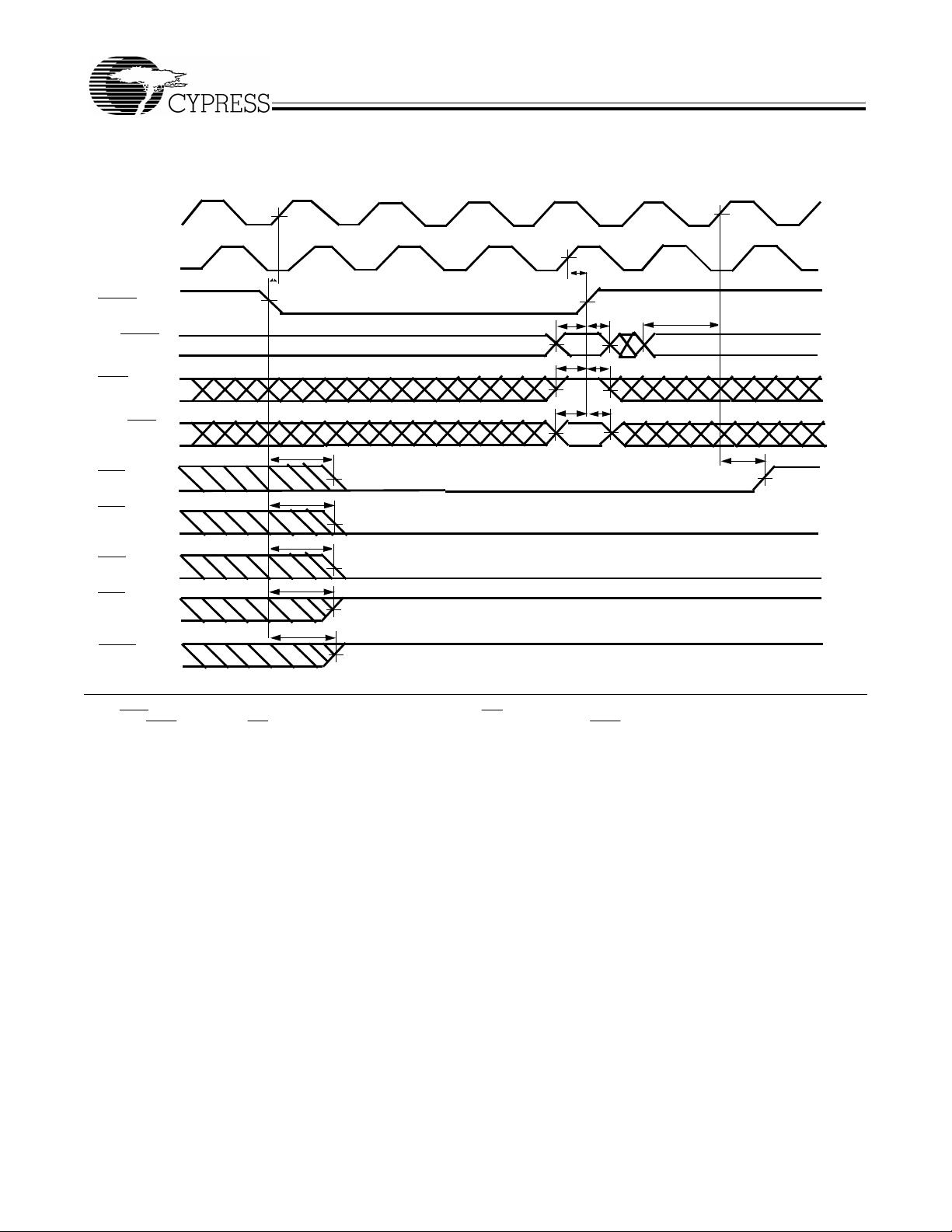
FIFO1 Master Reset Loading X1 and Y1 with a Preset Value of Eight
CLKA
CLKB
t
RSTS
CY7C43646AV
CY7C43666AV/CY7C43686AV
[11, 12]
t
RSTS
MRS1
t
BES
t
BEH
BE/FWFT
t
SPMS
t
SPMH
SPM
t
FSS
t
FSH
FS1, FS0
t
RSF
/IRA
FFA
t
t
RSF
RSF
EFB
/ORB
AEB
t
RSF
AFA
t
RSF
MBF1
Notes:
11. PRS1
12. If BE/FWFT is HIGH, then EFB/ORB will go LOW one CLKB cycle earlier than the case where BE/FWFT is LOW.
and MBC must be HIGH during Master Reset until the rising edge of FFA/IRA goes HIGH.
t
FWS
t
WFF
10
PRELIMINARY
CY7C43646AV
CY7C43666AV/CY7C43686AV
Switching Waveforms
(continued )
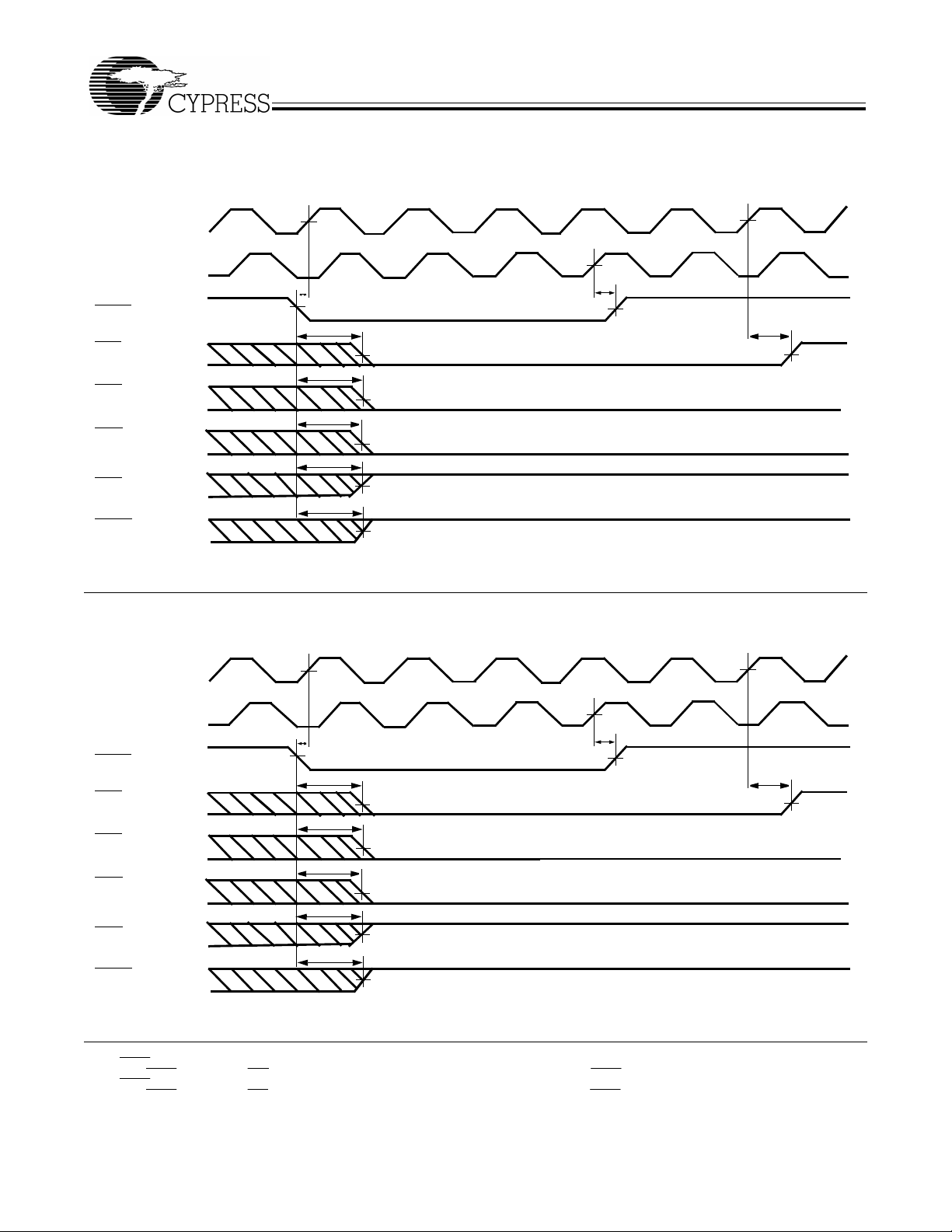
FIFO2 Master Reset Loading X1 and Y1 with a Preset Value of Eight
CLKC
CLKA
t
RSTS
MRS2
BE/FWFT
SPM
FS1/SEN,
FS0/SD
FFC
/IRC
EFA
/ORA
t
t
t
RSF
RSF
RSF
AEB
t
RSF
AFA
t
SPMS
t
t
BES
FSS
[13, 14]
t
RSTS
t
BEH
t
SPMH
t
FSH
t
FWS
t
WFF
t
RSF
MBF2
Notes:
13. PRS2
14. If BE/FWFT is HIGH, then EFA/ORA will go LOW one CLKA cycle earlier than the case where BE/FWFT is LOW.
and MBC must be HIGH during Master Reset until the rising edge of FFC/IRC goes HIGH.
11
PRELIMINARY
CY7C43646AV
CY7C43666AV/CY7C43686AV
Switching Waveforms
(continued )
FIFO1 Partial Reset (CY Standard and FWFT Modes)
CLKA
CLKB
t
RSTS
PRS1
t
RSF
FFA/IRA
t
RSF
EFB
/ORB
t
RSF
AEB
t
RSF
AFA
t
RSF
MBF1
[15, 16]
t
RSTH
t
WFF
FIFO2 Partial Reset (CY Standard and FWFT Modes)
[17, 18]
CLKC
CLKA
t
RSTS
t
RSTH
PRS2
t
RSF
FFC/IRC
t
RSF
EFA
/ORA
t
RSF
AEA
t
RSF
AFC
t
RSF
MBF1
Notes:
15. MRS1
16. If BE/FWFT is HIGH, then EFB/ORB will go LOW one CLKB cycle earlier than the case where BE/FWFT is LOW.
17. MRS2 must be HIGH during Partial Reset.
18. If BE/FWFT is HIGH, then EFA/ORA will go LOW one CLKA cycle earlier than the case where BE/FWFT is LOW.
must be HIGH during Partial Reset.
t
WFF
12
 Loading...