

Cypress Semiconductor CY7C43683-7AC, CY7C43663-7AC, CY7C43663-15AC, CY7C43663-10AC, CY7C43683-15AC Datasheet
...
Synchronous FIFO w/ Bus Matching
Features
• High-speed, lo w-power, Unidirectional, First-in Firstout (FIFO) memories w/bus matching capabili ties
• 1Kx36 (CY7C43643)
• 4Kx36 (CY7C43663)
• 16Kx36 (CY7C43683)
• 0.35-micron CMOS for optimum speed/power
• High-speed 133-MH z operation (7.5 ns read /write cyc le
times)
•Low power
—I
= 100 mA
CC
= 10 mA
—I
SB
Logic Block Diagram
CY7C43643
CY7C43663
CY7C43683
1K/4K/16K x36 Unidirectional
• Fully asynchronous and simultaneous read and write
operation permitted
• Mailbox bypass register for each FIFO
• Parallel and Serial Programmable Almost Full and
Almost Empty flags
• Retransmit func tion
• Standard or FWFT mode user selectable
• Partial Reset
• Big or Little Endian f ormat for word or byte bus sizes
• 128-pin TQFP packaging
• Easily expandable in width and depth
CLKA
CSA
W/RA
ENA
MBA
RT
MRS1
MRS2
PRS
FF/IR
AF
SPM
FS0/SD
FS1/SEN
A
0–35
MBF2
Port A
Control
Logic
FIFO,
Mail1
Mail2
Reset
Logic
36
Input
Register
Write
Pointer
Programmable
Flag Offset
Registers
Mail1
Register
1K/4K/16K
x36
Dual Ported
Memory
Status
Flag Logic
Timing
Mode
Mail2
Register
Read
Pointer
Bus Matching
Output
MBF1
CLKB
Port B
Control
Register
Logic
36
CSB
W/RB
ENB
MBB
BE
BM
SIZE
EF/OR
AE
B
0–35
BE/FWFT
Cypress Semiconductor Corporation
• 3901 North First Street • San Jose • CA 95134 • 408-943-2600
July 28, 2000
CY7C43643
CY7C43663
CY7C43683
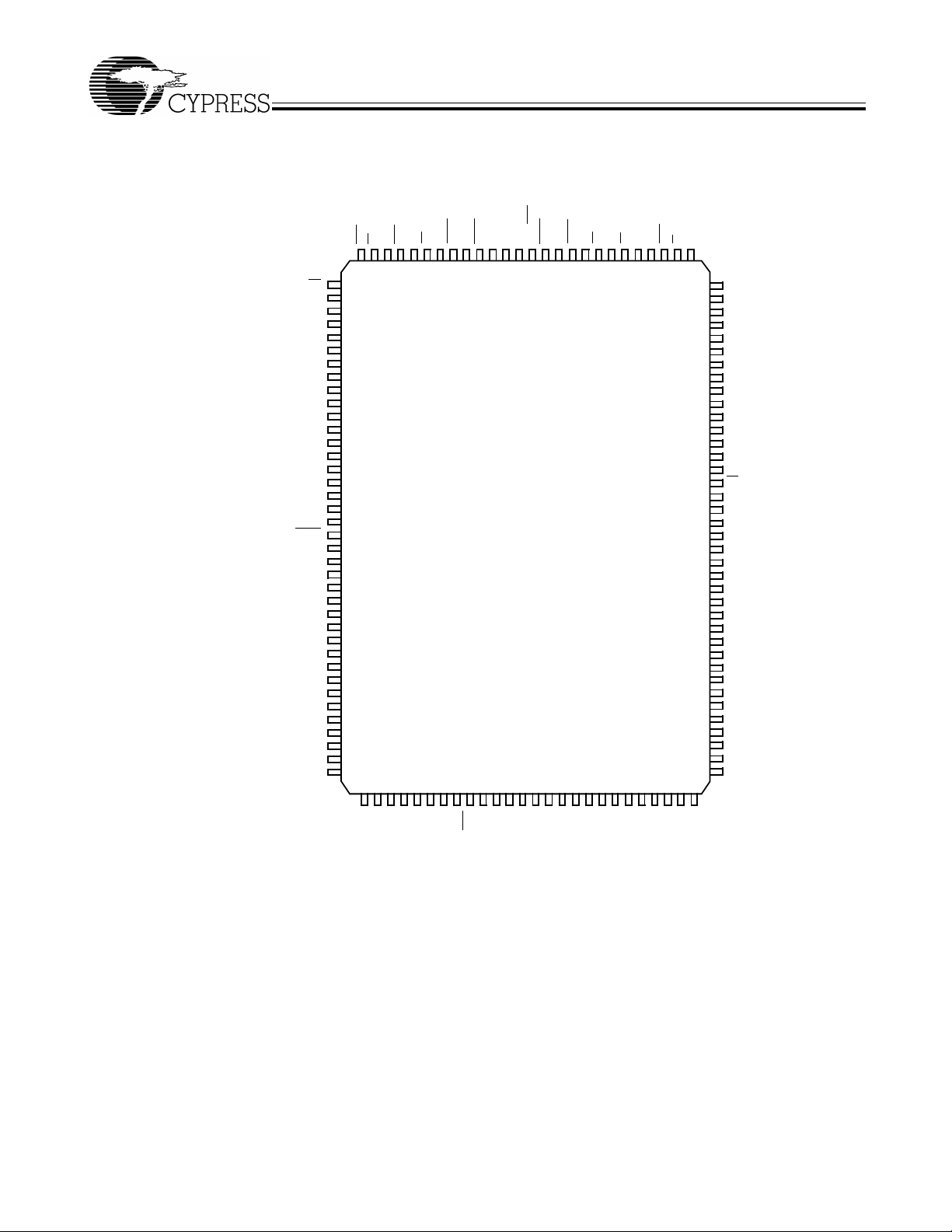
Pin Configuration
BE/FWFT
W/RA
ENA
CLKA
GND
A
A
A
A
V
A
A
GND
A
A
A
A
A
A
A
GND
A
V
A
A
A
A
GND
A
A
A
A
A
V
A
GND
A
A
TQFP
Top View
CSB
GND
CSA
FF/IR
NC
128
127
126
1
2
3
125
MBF2NCAF
FS0/SD
FS1/SEN
GND
GND
MRS1
VCCPRS
124
MBA
123
122
121
120
119
118
117
116
115
VCCMBF1
MRS2
MBB
114
113
112
111
4
5
35
6
34
7
33
32
8
9
CC
10
31
11
30
12
29
13
14
28
15
27
26
16
25
17
24
18
19
23
20
21
22
22
CC
23
21
24
20
25
19
26
18
27
28
17
29
16
30
15
31
14
32
13
33
CC
34
12
35
36
11
37
10
38
CY7C43643
CY7C43663
CY7C43683
39404142434445464748495051525354555657585960616263
9
5
A6A7A8A
GND
2
A
A3A4A
CC
V
SPM
0
1
1
B
A0A
GND
NC
EF/OR
NC
AE
110
109
108
107
ENB
W/RB
106
105
104
103
102
CLKB
101
V
CC
V
100
CC
99
B
35
98
B
34
97
B
33
96
B
32
GND
95
GND
94
93
B
31
92
B
30
91
B
29
90
B
28
89
B
27
88
B
26
RT
87
86
B
25
B
85
24
BM
84
83
GND
82
B
23
81
B
22
80
B
21
B
79
20
B
78
19
77
B
18
76
GND
B
75
17
74
B
16
SIZE
73
V
72
CC
B
71
15
B
70
14
69
B
13
B
68
12
GND
67
B
66
11
B
65
10
64
7
6
B
B5B4B3B2B
GND
B9B8B
CC
V
2
CY7C43643
CY7C43663
CY7C43683
Functional Description
The CY7C436x3 is a monolithic, high-speed, low-power,
CMOS Unidirectional Synchronous (clocked) FIFO memory
which supports clock fr equencies up to 133 MHz and has read
access times as fast as 6 ns. Two independent 1K/4K/16K x
36 dual-port SRAM FIFOs on board each chip buffer data in
opposite directions. FIFO data on Port B can be output in 36bit, 18-bit, or 9-bit formats with a choice of Big or Little Endian
configurations.
The CY7C436x3 is a synchronous (clocked) FIFO, meaning
each port employs a synchronous interface. All data tran sfers
through a port are gated to the LOW-to-HIGH transition of a
port clock by enable signals. The clocks for each port are independent of one another and can be asynchronous or coincident. The enables for each port are arranged to provide a
simple unidirectional interface between microprocessors and/
or buses with synchronous control.
Communicat ion betw een ea ch port may b ypa ss the FIF Os vi a
two mailbox registers. The mailbox registers’ width matches
the selected P o rt B bus width. Each mailbo x registe r has a flag
(MBF1
and MBF2) to signal when new mail has been stored.
Two kinds of reset are available on the CY7C436x3: Master
Reset and P artial Reset. Mast er Reset init iali zes t he read and
write pointers to the first location of the memory array, configures the FIFO for Big or Little Endian byte arrangement and
selects serial f lag programming, parallel flag prog ramming, or
one of the three possible default flag offset settings, 8, 16, or
64. The FIFO also has two Master Reset pins, MRS1
MRS2
.
Partial Reset also sets the read and write pointers to the first
location of the mem ory. Unlike Master Reset, any settings existing prior to P artial Reset ( i.e., pr ogr amming method a nd partial flag default offsets) are retained. Partial Reset is useful
since it permits fl ushing of the FI FO memory witho ut chang in g
any configuration settings. The FIFO has its own i ndependent
Partial Reset pi n, PRS
The CY7C436x3 have two modes of o peratio n: In t he CY Standard Mode, the fir st word written to an empty FIFO is deposited
into the memory array. A read operation is required to access
that word (along with all other words residing in memory). In
.
and
the First-Word F all-Through Mode (FWFT), the first long-word
(36-bit wide) written to an empty FIFO appears automatically
on the outputs, no read operation required (nevertheless, accessing subsequent words does necessitat e a f ormal read re quest). The state of the BE/FWFT
determines the mode in use.
The FIFO has a combined Empty/Output Ready flag (EF
and a combi ned Full/Input Ready flag (FF
functions a re selected in the CY Standard Mode. EF indicat es
whether the memory is full or not. The IR and OR funct ions are
selected in the First-Word Fall-Through Mode. IR indicates
whether or not the FIFO has available memory locations. OR
shows whether the FIFO has dat a av ai labl e f or readi ng or not.
It marks the presence of valid data on the outputs. (See footnote #18)
The FIFO has a programm able Almost Empty flag (AE
programmab le Almost Full flag (AF
lected number of words written to FIFO memory achieve a
predetermined “almost empty state.” AF
lected number of words written to the memory achieve a predetermined “almost full state.” (See footnote #34)
IR and AF
into its array. OR and AE
that reads data fro m its arr a y. Pro grammab l e offs et f or AE
AF
SD input. Three default offset settings are also provided. The
AE
empty boundary and AF
locations from the full boundary. All these choices are made
using the FS0 and FS1 inputs during Master Reset.
Two or more devices may be used in parallel to create wider
data paths. If any time the FIFO is not actively performing a
function, the chip will automatically power down. During the
power-down state, supply current consumption (I
minimum. Init iating a ny oper ati on (b y act iv ati ng con trol inputs )
will immediately take the device out of t he power-down state .
The CY7C436x3 are characterized for operation from 0°C to
70°C commercial, and from –40°C to 85°C industrial. Input
ESD protection is gr eater than 2001V, and latch-up is pr evented by the use of guard rings.
are synchronized to the port clock that writes data
are synchronized to the port clock
can be loaded in parallel using Port A or i n serial via the
threshold can be set at 8, 16, or 64 locations from the
threshold can be set at 8, 16, or 64
pin during FIFO operation
) is at a
CC
/OR)
) and a
and
/IR). The EF and FF
). AE indicates when a se-
indicates when a se-
Selectio n Gu ide
CY7C43643/63/83
Maximum Frequency (MHz) 133 100 66.7
Maximum Access Time (ns) 6 8 10
Minimum Cycle Time (ns) 7.5 10 15
Minimum Data or Enable Set-Up (ns) 3 4 5
Minimum Data or Enabl e Hold ( ns) 0 0 0
Maximum Flag Delay (ns) 6 8 8
Active Power Supply
Current (I
Density 1K x 36 4K x 36 16K x 36
Package 128 TQFP 128 TQFP 128 TQFP
CC1
) (mA)
Commercial 100 100 100
Industrial 100
7
–
CY7C43643 CY7C43663 CY7C43683
3
CY7C43643/63/83
–10
CY7C43643/63/83
15
–
CY7C43643
CY7C43663
CY7C43683
Pin Definitions
Signal Name Description I/O Function
A
0–35
AE
AF
B
0–35
BE/FWFT
BM Bus Match
CLKA Port A Clock I CLKA is a continu ous cloc k that sy nchroniz es al l data tr ansfer s through P ort A and can
CLKB Port B Clock I CLKB is a continuous clock t hat synchr onizes al l data t ransf ers thr ough P ort B and can
CSA
CSB
EF
/OR Empty/Output
ENA Port A Enable I ENA must be HIGH to enable a LOW- to-HIGH tr ansit ion of CLKA t o read or write data
ENB Port B Enable I ENB must be HIGH to enable a LOW- to-HIGH tr ansit ion of CLKB t o read or write data
FF
/IR Port B Full/Input
FS1/SEN
FS0/SD Flag Offset
Port A Data I 36-bit unidirectional data port for side A.
Almost Empty
Flag (Port B)
Almost Full Flag O Progr am m able Almost Full flag synchroniz ed to CLKA. It is LOW when the num ber of
Port B Data O 36-bit unidirectional data port for side B.
Big Endian/
First-Word FallThrough Select
Select (Port B)
Port A Chip
Select
Port B Chip
Select
Ready Flag
(Port B)
Ready Flag
Flag Offset
Select 1/Serial
Enable
Select 0/Serial
Data
O Programmab le Almost Empty flag synchronized to CLKA. It is LO W when the numb er
of words in the FIFO2 is less than or equal to the value in the Almost Empty A offset
register, X. (See foot note #.)
empty locations in t he FIFO is less tha n or equal to the v alue in t he Almost Full A off set
register, Y. (See f ootnote #.)
I This is a dual-purpose pin. During Master Reset, a HIG H on BE will selec t Big Endian
operation. In thi s case, depe nding on the bus size, the most signi ficant byt e or word on
Port A is transf err ed to P ort B first. A LO W on BE will select Little Endi an opera tion. In
this case, the l eas t signif icant b yte or w ord on Port A is transferred to P ort B fir st. Af ter
Master Reset, this pin select s the timing mode. A HI GH on FWFT
Mode, a LO W sel ects Fi rst- W ord Fall-Thr ough Mo de. Onc e th e timi ng mode h as been
selected, the level on FWFT
I A HIGH on this pin enables eith er byt e or w ord bus width on Port B, depending on the
state of SIZE. A LOW select s long-word operation. BM works with SIZE and BE to
select the bus size and endian arrangement for Port B. The level of BM must be static
throughout device operation.
be asynchronous or coincident to CLKB. FF
to-HIGH transition of CLKA.
be asynchronous or coincident to CLKA. FB
nized to the LO W-to-HIGH tran sition of CLKB.
ICSA must be LOW to enable a LOW-t o HIGH tr ansition of CLKA to read or write on
Port A. The A
ICSB must be LOW to enable a LOW-t o HIGH tr ansition of CLKB to read or write on
Port B. The B
O This is a dual-function pin. In the CY Standard Mode, the EF function is selected. EF
indicates whether or not the FIFO memory is empty . In the FWFT mode, the OR function
is selected. OR indicates the presence of valid data on A
reading. EF
#34.)
on Port A.
on Port B.
O This is a dual-function pin. In the CY Standard Mode, the FF function is selected. FF
indicates whether or not the FIFO memory is full. In the FWFT mode, the IR function
is selected. IR indi cates whet her or not there is spac e a v aila ble f or writing to the FIFO
memory. FF
I FS1/SEN and FS0/SD are dual-purpose input s used for flag offset regi ster program-
ming. During Master Reset, FS1/SEN
offset program ming method. Three offs et register progr amming methods are a vailab le:
automatically load one of three preset v alues (8, 16, or 64), par allel load from Port A,
I
and serial load. When serial load i s select ed f or flag offs et regi ster pr ogr amming , FS1/
SEN
is used as an enab le synchron ous to the LO W- to-HIGH tr ansition of CLKA. When
FS1/SEN
and Y registers . The numbe r of bi t writes r equi red t o progr am t he off set re gister s is 2 0
for the CY7C43643, 24 for the CY7C43663, and 28 for the CY7C43683. The first bit
write stores the Y-register MSB and the last bit write stores t he X-register LSB.
is LOW, a rising edge on CLKA loads the bit present on FS0/SD into the X
outputs are in the high-im pedance state when CSA is HIGH.
0–35
outputs are in the high- impedance state when CSB is HIGH.
0–35
/OR is synchr onized t o the LO W -to-HIGH t ransit ion of CLKB . (See f o otnote
/IR is synchronized to the LOW-to-HIGH transit ion of CLKA.
must be static throughout device operation.
/IR and AF are all synchronize d to the LO W-
/IR, EF /OR, AF, and AE are all synchro-
and FS0/SD , together with SPM, sel ect the flag
selects CY Standar d
outputs, available for
0–35
4
CY7C43643
CY7C43663
CY7C43683
Pin Definitions
Signal Name Description I/O Function
MBA P ort A Mailbox
MBB P ort B Mailbox
MBF1
MBF2
MRS1
MRS2
PRS
RT
SIZE Bus Size Select I A HIGH on this pin when BM is HIGH selects byte bus (9-bit) si ze on Port B. A LOW
SPM
W/RA
RB Port B Write/
W/
(continued)
Select
Select
Mail1 Register
Flag
Mail2 Register
Flag
Master Reset I A LOW on this pin initializes the FIFO read and write pointers to the fi rst location of
Master Reset I A LOW on this pin initiali zes the Mail2 register.
Partial Reset I A LOW on this pin initializes the FIFO read and write pointers to the first location of
Retransmit I A LOW str obe o n thi s pin will retran smit data on t he FIFO. This is achi e v ed b y bringing
Serial
Programming
Port A Write/
Read Select
Read Select
I A HIGH lev el on MBA chooses a mail box register for a Port A read or write operation.
I A HIGH lev el on MBB chooses a mail box register for a Port B read or write operation.
When a read operatio n is perf ormed on Port B, a HIGH lev el on MBB select s data from
the Mail1 register for output and a LOW level selec ts FIFO output register data for
output. Data can only be written into Mail 2 reg ister through Port B (MBB HIGH) and
not into the FIFO memory.
OMBF1 is set LOW by a LOW-to-HIGH tr ansition of CLKA that writes data to the Mail1
register. Writes to the Mail1 register are inhibited while MBF1
HIGH by a LOW-to-HIGH transitio n of CLKB when a Port B read is selected and MBB
is HIGH. MBF1
OMBF2 is set LOW by a LOW-to-HIGH tr ansition of CLKB that writes data to the Mail2
register. Writes to the Mail2 register are inhibited while MBF2
HIGH by a LOW-to-HIGH transitio n of CLKA when a Port A read is selected and MBA
is HIGH. MBF2
memory and sets the P ort B output register to al l zeroes . A LOW puls e on MRS1
the programmi ng method (serial or parallel ) and one of three p rogrammab le flag def ault
offsets. It al so configures Port B for bus size and endian arrangement. Four LOW -toHIGH transitio ns of CLKA and f our LO W-t o-HIGH tr ansitions of CLKB m ust occur while
MRS1
is LOW.
memory and sets the Port B output register to all zeroes. During Partial Reset, the
currently selected bus size, endian arrangement, programming method (serial or par allel), and progr am m able flag settings are all retained.
the read pointer bac k to loc ation zer o . The user will still need to perf orm read operat ion
to retransmit the dat a. Retransmit function applies to CY standard mode only.
on this pin when BM is HIGH selec ts word (18-bit) bus size. SIZE works with BM and
BE to select the bus size and endian arrangement for Port B. The level of SIZE must
be static throughout device operation.
I A LOW on this pin se lects serial p rogrammin g of partial flag offs ets. A HIGH on t his pin
selects paral lel programming or default offsets (8 , 16, or 64).
I A HIGH selects a write operation and a LOW selects a read operat ion on Port A for a
LOW-to-HIGH transition of CLKA. The A
when W/RA
I A LOW selects a write operation and a HIGH selects a read operation on Port B for a
LOW-to-HIGH transit ion of CLKB. The B
when W
is set HIGH following either a Master or Partial Reset.
is set HIGH following either a Master or P arti al Reset of FIFO2.
outputs are in the high-impedance state
is HIGH.
/RB is LOW.
0–35
outputs are in the high-impedance state
0–35
is LOW. MBF1 is set
is LOW. MBF2 is set
selects
5
CY7C43643
CY7C43663
CY7C43683
Maximum Ratings
[1]
(Abov e which the useful life may be impaired. F or user guidelines, not tested.)
Storage Temperature ............. .......... ... .........–65
°
C to +150°C
Ambient Temperature with
Power Applied ...............................................–55
°
C to +125°C
Output Current into Outputs (LOW)............................. 20 mA
Static Discharge Voltage.......... ............. .. ..................>2001V
(per MIL-STD-883, Method 3015)
Latch -U p Cu rre n t....... ......... .......... .......... ......... ......... >200mA
Operating Range
Supply Voltage to Gr o u nd Potent ia l ..... ......... . –0.5V to +7.0V
DC Voltage Applied to Outputs
in High Z State
DC Input Voltage
Electrical Characteristics
[2]
......................................–0.5V to VCC+0.5V
[2]
...................................–0.5V to VCC+0.5V
Over the Operating Range
Parameter Description Te st Condi tions
V
V
V
V
I
IX
I
OZL
I
OZH
I
CC1
I
SB
OH
OL
IH
IL
[4]
[5]
Output HIGH Voltage VCC = 4.5V,
I
= –4.0 mA
OH
Output LO W Voltage VCC = 4.5V,
I
= 8.0 mA
OL
Input HIGH Voltage 2.0 V
Input LOW Vol tage –0.5 0.8 V
Input Leakage Curr ent V
Output OFF, High Z
Current
= Max. –10 +10 µA
CC
OE > VIH,
V
< VO< V
SS
Active Power Supply
Current
Average Standb y
Current
Range
Ambient
Temperature V
CC
[3]
Commercial 0°C to +70°C 5.0V ± 0.5V
Industrial –40°C to +85°C 5. 0V ± 0.5V
CY7C43643/63/83
2.4 V
0.5 V
CC
–10 +10
CC
Com’l 100 mA
Ind 100 mA
Com’l 10 mA
Ind 10 mA
UnitMin. Max.
V
µA
Capacitance
[6]
Parameter Description Te st Condi tions Max. Unit
C
IN
C
OUT
Notes:
1. Stresses beyond those listed under “Absolute Maximum Ratings” may cause permanent damage to the device. These are stress ratings only and functional
operation of the device at these or any other conditions beyond those indicated under “recommended operating conditions” is not implied. Exposure to absolutemaximum-rated conditions for extended periods may affect device reliability.
2. The input and output voltage ratings may be exceeded provided the input and output current ratings are observed.
3. Operating V
4. Input signals switch from 0V to 3V with a rise/fall time of less than 3 ns, clocks and clock enables switch at 20 MHz, while data inputs switch at 10 MHz. Outputs
are unloaded.
5. All inputs = V
6. Tested initially and after any design or process changes that may affect these parameters.
range for -7 speed is 5.0V ±0.25V.
CC
– 0.2V, except RCLK and WCLK (which are at frequency = 0 MHz). All outputs are unloaded.
CC
Input Capacitance TA = 25°C, f = 1 MHz,
V
= 3.3V
Outp u t C a pacit a nce 8 pF
CC
4 pF
6
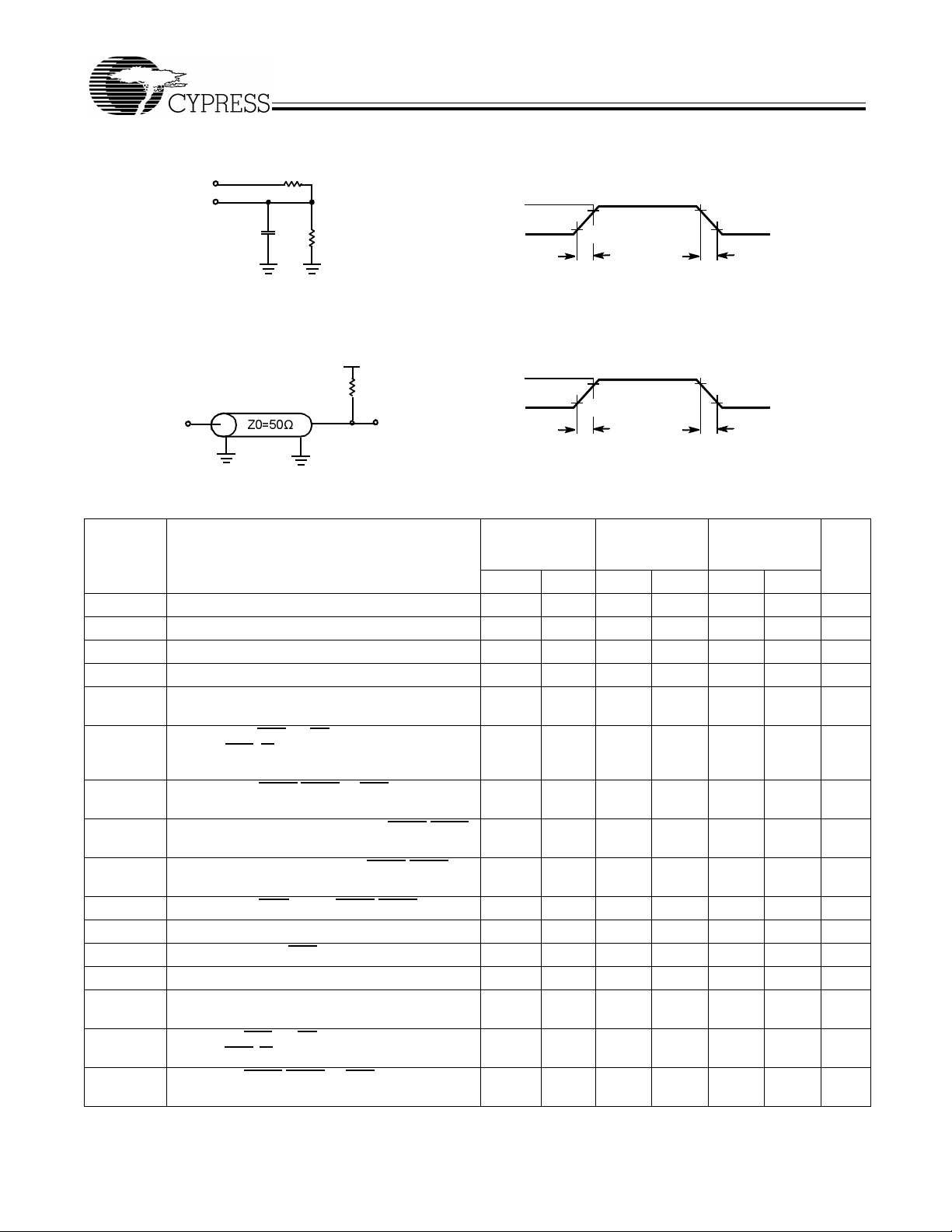
AC Test Loads an d Waveforms (-1 0 & -15)
CY7C43643
CY7C43663
CY7C43683
5V
OUTPUT
INCLUDING
C
=30 pF
L
JIG AND
SCOPE
R1=1.1K
Ω
R2=680
Ω
AC Test Loads and Waveforms (-7)
VCC/2
50Ω
I/O
Switching Characteristics
Parameter Description
f
S
t
CLK
t
CLKH
t
CLKL
t
DS
t
ENS
t
RSTS
t
FSS
t
BES
t
SPMS
t
SDS
t
SENS
t
FWS
t
DH
t
ENH
t
RSTH
Note:
7. Requirement to count the clock edge as one of at least four needed to reset a FIFO.
Clock Frequency, CLKA or CLKB 133 100 67 MHz
Clock Cycle Time, CLKA or CLKB 7.5 10 15 ns
Pulse Duration, CLKA or CLKB HIGH 3.5 4 6 ns
Pulse Duration, CLKA or CLKB LO W 3.5 4 6 ns
Set-Up Time, A
before CLKB↑
Set-Up Time, CSA, W/RA, ENA, and MBA before
CLKA↑; CSB
CLKB↑
Set-Up Time, MRS1/MRS2 or PRS LOW before
CLKA↑ or CLKB↑
Set-Up Time, FS0 and FS1 before MRS1/MRS2
HIGH
Set-Up Time, BE/FWFT before MRS1/MRS2
HIGH
Set-Up Time, SPM before MRS1/MRS2 HIGH 5 7 7.5 ns
Set-Up Time, FS0/SD before CLKA↑ 3 4 5 ns
Set-Up Time, FS1/SEN before CLK A↑ 3 4 5 ns
Set-Up Time, FWFT before CLKA↑ 0 0 0 ns
Hold Time, A
CLKB↑
Hold Time, CSA, W/RA, ENA, and MBA after
CLKA↑; CSB
Hold Time, MRS1/MRS2 or PRS LOW after
CLKA↑ or CLKB↑
=
Ω
Over the Operating Range
before CLKA↑ and B
0–35
0–35
, W/RB, ENB, and MBB before
[7]
after CLK A↑ and B
0–35
0–35
after
, W/RB, ENB, and MBB after CLKB↑
[7]
ALL INPUT PULSES
3.0V
GND
≤
90%
10%
3ns
90%
10%
3
ns
≤
ALL INPUT PULSES
3.0V
GND
3ns
≤
CY7C43643/
63/83
–7
90%
10%
CY7C43643/
63/83
–10
90%
10%
3 ns
≤
CY7C43643/
63/83
–15
3 4 5 ns
3 4 5 ns
2.5 4 5 ns
6 7 7.5 ns
5 7 7.5 ns
0 0 0 ns
0 0 0 ns
1 2 4 ns
UnitMin. Max. Min. Max. Min. Max.
7
CY7C43643
CY7C43663
CY7C43683
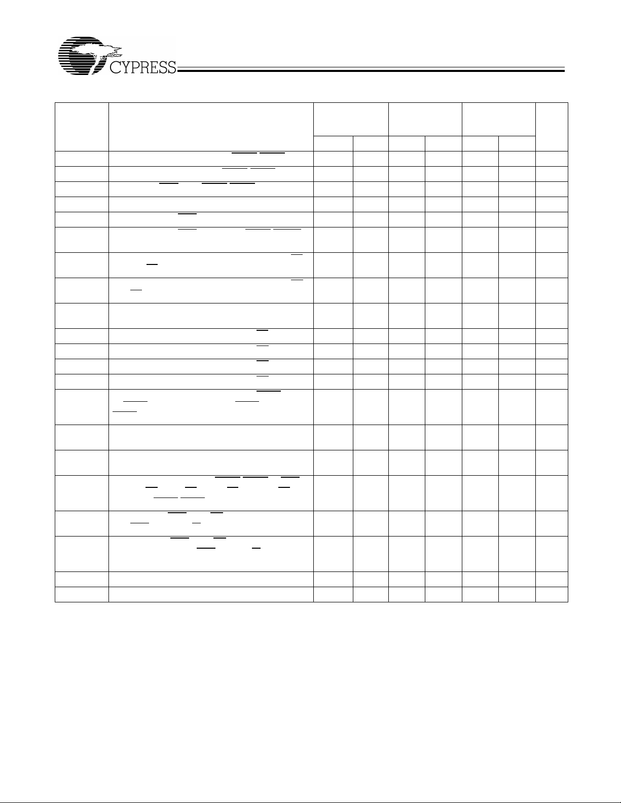
Switching Characteristics
Over the Operating Range (continued)
CY7C43643/
63/83
–7
CY7C43643/
63/83
–10
CY7C43643/
63/83
–15
Parameter Description
t
FSH
t
BEH
t
SPMH
t
SDH
t
SENH
t
SPH
t
SKEW1
t
SKEW2
Hold Time, FS0 and FS1 after MRS1/MRS2 HIGH 1 1 2 ns
Hold Time, BE/FWFT after MRS1/MRS2 HIGH 1 1 2 ns
Hold Time, SPM after MRS1/MRS2 HIGH 1 1 2 ns
Hold Time, FS0/SD after CLKA↑ 0 0 0 ns
Hold Time, FS1/SEN after CLKA↑ 0 0 0 ns
Hold Time, FS1/SEN HIGH after MRS1/MRS2
0 1 2 ns
HIGH
[8]
Skew Time between CLKA↑ and CLKB↑ for EF /
OR and FF
[8]
Skew Time between CLKA↑ and CLKB↑ for AE
/IR
5 5 7.5 ns
7 8 12 ns
and AF
t
A
t
WFF
t
REF
t
PAE
t
PAF
t
PMF
t
PMR
t
MDV
t
RSF
t
EN
t
DIS
t
PRT
t
RTR
Notes:
8. Skew time is not a timing constraint for proper device operation and is only included to illustrate the timing relationship between the CLKA cycle and the CLKB
cycle.
9. Writing data to the Mail1 register when the B
10. Writing data to the Mail2 register when the A
Access Time, CLKA↑ to A
B
0–35
and CLKB↑ to
0–35
1 6 1 8 3 10 ns
Propagation Delay Time, CLKA↑ to FF/IR 1 6 1 8 2 8 ns
Propagation Delay Time, CLKB↑ to EF/OR 1 6 1 8 1 8 ns
Propagation Delay Time, CLKB↑ to AE 1 6 1 8 1 8 ns
Propagation Delay Time, CLKA↑ to AF 1 6 1 8 1 8 ns
Propagation Delay Time, CLKA↑ to MBF1 LOW
or MBF2
MBF1
Propagation Delay Time, CLKA↑ to B
CLKB↑ to A
Propagation Dela y Time, MBA to A
MBB to B
HIGH and CLKB↑ to MBF2 LOW or
HIGH
0–35
0–35
0–35
0–35
Valid
[10]
[9]
and
V alid an d
Propagation Delay Time, MRS1/MRS2 or PRS
LOW to AE
LOW and MBF1
Enable Time, CSA or W/RA LOW to A
and CSB
Disable Time, CSA or W/RA HIGH to A
High Impedance and CSB
B
0–35
LOW, AF HIGH, FF/IR LOW, EF/OR
/MBF2 HIGH
LOW and W/RB HIGH to B
HIGH or W/RB LOW to
at High Impedance
0–35
0–35
Active
Active
0–35
at
0 6 0 8 0 12 ns
1 7 2 11 3 12 ns
1 6 2 9 3 11 ns
1 6 1 10 1 15 ns
1 6 2 8 2 10 ns
1 5 1 6 1 8 ns
Retransmit Pulse W idt h 60 60 60 ns
Retransmit Recovery Time 90 90 90 ns
outputs are active and MBB is HIGH.
0–35
outputs are active and MBA is HIGH.
0–35
UnitMin. Max. Min. Max. Min. Max.
8
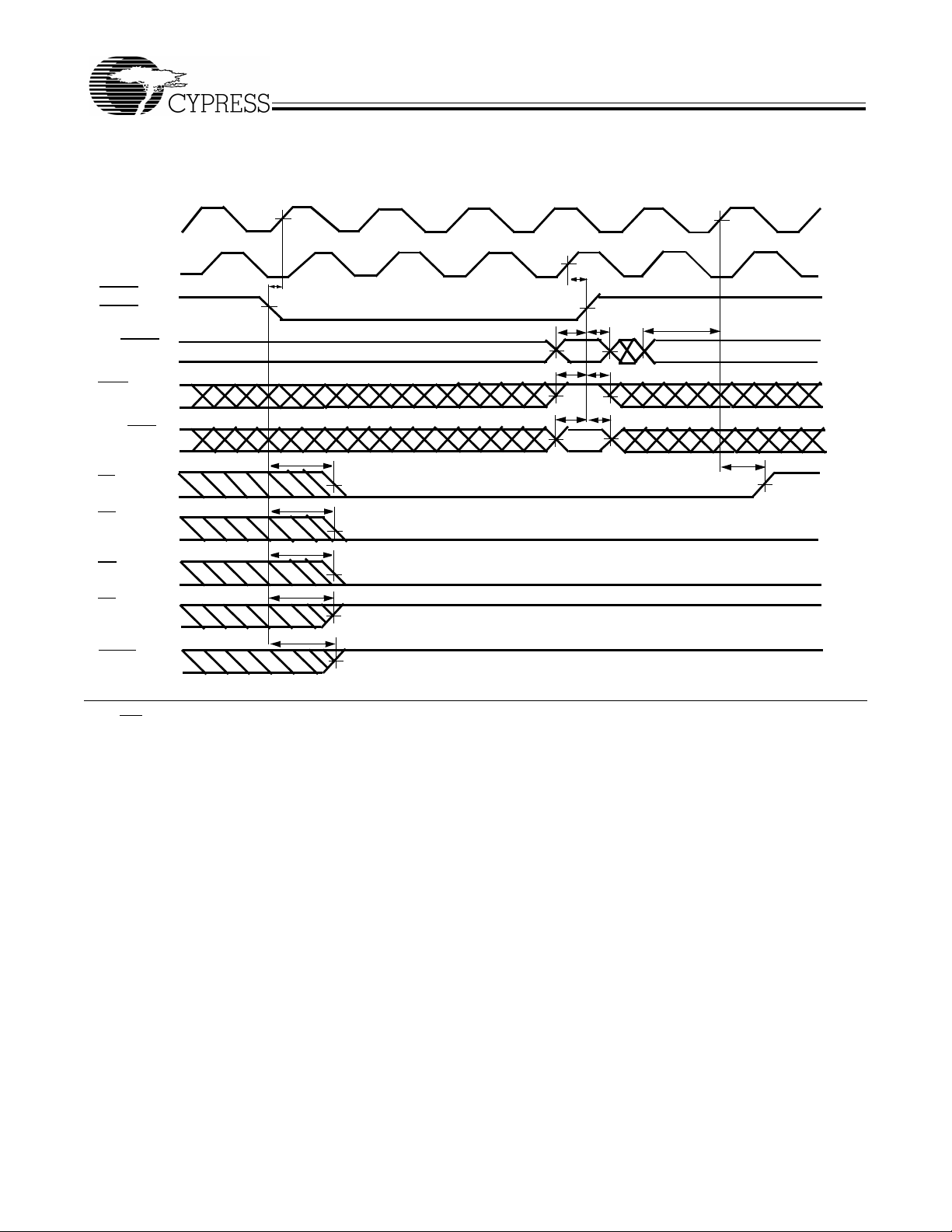
Switching Waveforms
Master Reset Loading X and Y with a Preset Value of Eight
CLKA
CLKB
t
,
MRS1
MRS2
BE/FWFT
SPM
FS1/SEN,
FS0/SD
FF
/IR
EF
/OR
RSTS
t
t
RSF
RSF
[11]
t
SPMS
t
BES
t
FSS
t
RSTH
t
BEH
t
SPMH
t
FSH
t
FWS
CY7C43643
CY7C43663
CY7C43683
t
WFF
AE
AF
MBF1
Note:
11. PRS
t
RSF
t
RSF
t
RSF
must be HIGH during Master Reset.
9
 Loading...