

Page 1

PCB-4300
Installation and Operation Manual
1:2 Phase Combiner
IMPORTANT NOTE: The information contained in this document supersedes all previously published
information regarding this product. Product specifications are subject to change without prior notice.
Part Number MN/PCB4300.IOM Revision 2
Page 2

Page 3

PCB-4300
1:2 Phase Combiner
Installation and Operation Manual
Part Number MN/PCB4300.IOM
Revision 2
April 29, 2010
Copyright © 2010 Comtech EF Data. All rights reserved. Printed in the USA.
Comtech EF Data, 2114 West 7th Street, Tempe, Arizona 85281 USA, 480.333.2200, FAX: 480.333.2161
Page 4

This page is intentionally blank.
ii
Page 5

Table of Contents
TABLE OF CONTENTS .............................................................................................................. III
TABLES ...................................................................................................................................... VI
FIGURES .................................................................................................................................... VI
PREFACE .................................................................................................................................. VII
About this Manual
Reporting Comments or Suggestions Concerning this Manual .............................................................. vii
Conventions and References ................................................................................................................... viii
Cautions and Warnings .......................................................................................................................... viii
Recommended Standard Designations ................................................................................................... viii
Trademarks ............................................................................................................................................ viii
Metric Conversion ................................................................................................................................. viii
Electrical Safety Notice ............................................................................................................................ viii
Warranty Policy ......................................................................................................................................... ix
Limitations of Warranty ........................................................................................................................... ix
Exclusive Remedies .................................................................................................................................. x
Customer Support ...................................................................................................................................... xi
Online Customer Support ........................................................................................................................ xi
CHAPTER 1. INTRODUCTION ............................................................................................. 1–1
1.1 Overview ...................................................................................................................................... 1–1
1.2 Functional Description ............................................................................................................... 1–2
.................................................................................................................................... vii
1.3 Theory of Operation ................................................................................................................... 1–4
1.3.1 Phase and Gain Equalization .................................................................................................... 1–4
1.3.2 System Switching ..................................................................................................................... 1–5
1.3.3 System Gain .............................................................................................................................. 1–6
1.3.4 System Attenuation ................................................................................................................... 1–6
1.4 Dimensional Envelope ................................................................................................................ 1–7
CHAPTER 2. EXTERNAL CONNECTORS ........................................................................... 2–1
2.1 Overview ...................................................................................................................................... 2–1
iii
Page 6

PCB-4300 1:2 Phase Combiner Revision 2
Table of Contents MN/PCB4300.IOM
2.2 Monitor and Control (M&C) Interface Connectors ................................................................ 2–3
2.2.1 SYSTEM COM J1 Connector .................................................................................................. 2–3
2.2.2 SSPA COM 1 J2, SSPA COM 2 J3, SSPA COM 3 J4 Connectors .......................................... 2–4
2.2.3 SSPA SW OUT J5 Connector .................................................................................................. 2–5
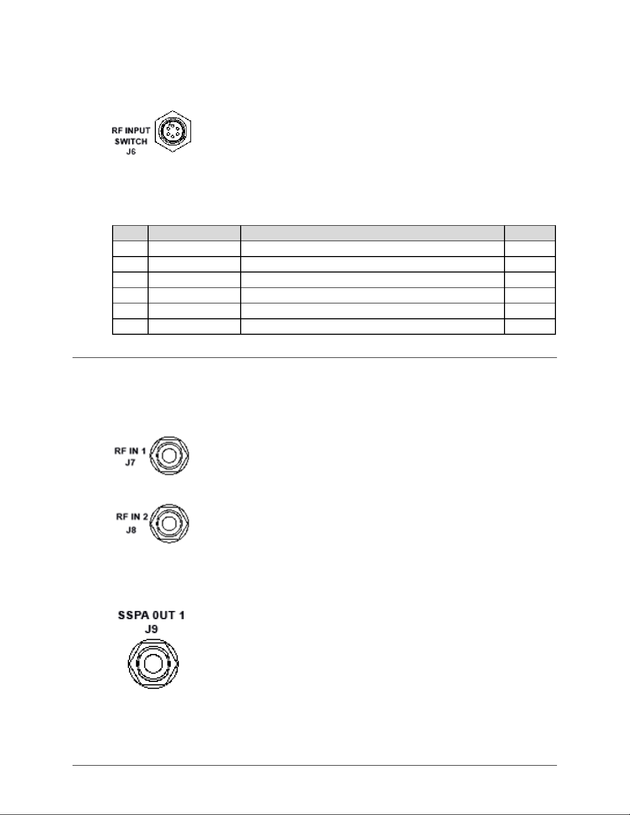
2.2.4 RF INPUT SWITCH J6 Connector .......................................................................................... 2–6
2.3 RF Interface Connectors ............................................................................................................ 2–6
2.3.1 RF IN 1 J7, RF IN 2 J8 Connectors .......................................................................................... 2–6
2.3.2 SSPA OUT 1 J9 Connector ...................................................................................................... 2–6
2.3.3 SSPA OUT 2 J10, SSPA OUT 3 J11 Connectors..................................................................... 2–7
2.4 Power and Ground Interfaces .................................................................................................... 2–7
2.4.1 AC Power ................................................................................................................................. 2–7
2.4.2 Ground Connector .................................................................................................................... 2–7
CHAPTER 3. OPERATION AND ADJUSTMENT PROCEDURES ....................................... 3–1
3.1 Overview ...................................................................................................................................... 3–1
3.2 System Assembly Example and Cable Connections ................................................................ 3–2
3.2.1 Installation ................................................................................................................................ 3–3
3.2.2 LED Status Operation ............................................................................................................... 3–4
3.3 System Verification ..................................................................................................................... 3–5
3.3.1 System Gain Verification ......................................................................................................... 3–5
3.3.2 System P1dB Verification ........................................................................................................ 3–6
3.4 Single Frequency Alignment (as necessary) ............................................................................. 3–7
3.4.1 Gain Equalization ..................................................................................................................... 3–7
3.4.2 Phase Equalization
.................................................................................................................... 3–8
3.5 Full Bandwidth Alignment (as necessary) .............................................................................. 3–10
3.5.1 Gain Equalization ................................................................................................................... 3–10
3.5.2 Phase Equalization .................................................................................................................. 3–11
CHAPTER 4. FLASH UPGRADING ...................................................................................... 4–1
4.1 Overview ...................................................................................................................................... 4–1
4.2 Flash Updating via Internet ....................................................................................................... 4–1
4.2.1 Firmware File Transfer Procedure ........................................................................................... 4–2
4.3 Flash Upgrade Procedure ........................................................................................................... 4–3
APPENDIX A. ASSEMBLY KITS ......................................................................................... A–1
A.1 Overview ..................................................................................................................................... A–1
A.2 Common Assembly Items .......................................................................................................... A–2
iv
Page 7

PCB-4300 1:2 Phase Combiner Revision 2
Table of Contents MN/PCB4300.IOM
A.2.1 Universal Pole Mounting Kit PL/12319-1 ............................................................................... A–2
A.2.2 Dual-Channel Unistrut Mounting Kit KT-0000017 ................................................................ A–3
A.2.3 HPOD Unistrut Mounting Kit KT/12300-1 ............................................................................. A–4
A.3 PCB-4300 Phase Combiner in Assemblies ............................................................................... A–5
A.4 PCB-4300 Ku-Band Unit (PL/11285-2) Assemblies ................................................................ A–6
A.4.1 Ku-Band 1:2 Phase Combined System Assembly – HPOD PL-0000317 ............................... A–6
A.4.1.1 Ku-Band 1:2 Phase Combined System – Waveguides and Components Kit KT-0000026 ....
........................................................................................................................................ A–10
A.4.2 Ku-Band 1:2 Phase Combined System Kit KT/11830-1 (Legacy Item) ............................... A–14
A.4.2.1 Ku-Band 1:2 Phase Combined System Kit KT/11830-1 – Assembly Examples ........... A–17
A.5 PCB-4300 C-Band Unit (PL-0000582) Assemblies ................................................................ A–22
A.5.1 C-Band 1:2 Phase Combined Top Assembly Kit – 350W HPOD (CEFD P/N KT-0000109) .......
............................................................................................................................................... A–22
A.5.1.1 C-Band 1:2 Phase Combined System Waveguide Kit – HPOD (CEFD P/N KT-0000107) ...
........................................................................................................................................ A–26
APPENDIX B. REMOTE CONTROL .................................................................................... B–1
B.1 Overview ..................................................................................................................................... B–1
B.2 EIA-485 ....................................................................................................................................... B–1
B.3 EIA-232 ....................................................................................................................................... B–2
B.4 Basic Protocol ............................................................................................................................. B–2
B.5 Packet Structure ......................................................................................................................... B–3
B.5.1 Start Of Packet ......................................................................................................................... B–3
B.5.2 Target (Base) Address ............................................................................................................. B–3
B.5.2.1 Virtual Address ................................................................................................................ B–4
B.5.3 Address Deli miter
.................................................................................................................... B–4
B.5.4 Instruction Code ...................................................................................................................... B–4
B.5.5 Instruction Code Qualifier ....................................................................................................... B–5
B.5.6 Optional Message Argu ments .................................................................................................. B–6
B.5.7 End Of Packet .......................................................................................................................... B–6
B.6 Remote Commands / Queries .................................................................................................... B–6
v
Page 8

PCB-4300 1:2 Phase Combiner Revision 2
Table of Contents MN/PCB4300.IOM
Tables
Table 2-1. PCB-4300 External Connectors ............................................................................................... 2–2
Table 2-2. Connector J1 Pinouts ............................................................................................................... 2–3
Table 2-3. Connector J2, J3, J4 Pinouts .................................................................................................... 2–4
Table 2-4. Connector J5 Pinouts ............................................................................................................... 2–5
Table 2-5. Connector J6 Pinouts ............................................................................................................... 2–6
Table A-1. PL-0000317 Assembly BOM ................................................................................................ A–6
Table A-2. KT-0000026 Kit BOM ........................................................................................................ A–10
Table A-3. Kit KT/11830-1 BOM ......................................................................................................... A–14
Table A-4. Kit KT-0000109 BOM ........................................................................................................ A–22
Table A-5. Kit KT-0000107 BOM ........................................................................................................ A–26
Figures
Figure 1-1. Comtech EF Data PCB-4300 1:2 Phase Combiner Control Box (PCCB) ............................. 1–1
Figure 1-2. Comtech EF Data 1:2 Phase Combined System Block Diagrams ......................................... 1–2
Figure 1-3. Combining Loss vs. Phase Imbalance Summary of Specifications ....................................... 1–4
Figure 1-4. PCB-4300 Dimensional Envelope ......................................................................................... 1–7
Figure 2-1. PCB-4300 External Connectors ............................................................................................. 2–1
Figure 3-1. PCB-4300 1:2 Phase Combined System Assembly Example ................................................ 3–2
Figure 3-2. PCB-4300 1:2 Phase Combined System Cable Connections ................................................. 3–2
Figure 3-3. PCB-4300 LED Status Panel .................................................................................................. 3–4
Figure 3-4. Phase Shifter Adjustment Locations ...................................................................................... 3–8
Figure 4-1. Flash Update via Internet ....................................................................................................... 4–1
Figure A-1. Universal Pole Mounting Kit, PL/12319-1 .......................................................................... A–2
Figure A-2. PCB-4300 Phase Combiner Box and Bracket Kits .............................................................. A–3
Figure A-3. HPOD Mounting Bracket Kit (CEFD P/N KT/12300-1) ..................................................... A–4
Figure A-4. PCB-4300 Phase Combiner Box and Bracket Kits .............................................................. A–5
Figure A-5. Ku-Band 1:2 Phase Combined Assembly – HPOD (CEFD P/N PL-0000317).................... A–7
Figure A-6. Ku-Band 1:2 Phase Combined Assembly – HPOD (CEFD P/N PL-0000317).................... A–8
Figu r e A-7. Ku-Band 1:2 Wave guides an d Compone n ts Kit (CEFD P/N KT-000 0 026) – Front View ...... A–12
Figu r e A-8. Ku-Band 1:2 Wave guides an d Compone n ts Kit (CEFD P/N KT-000 0 026) – Back View ...... A–13
Figure A-9. Ku-Band 1:2 Phase Combined System Kit KT/11830-1 (Legacy Item) ............................ A–16
Figure A-10. Ku-Band 1:2 Phase Combined System Kit KT/11830-1 – PCCB Cabling Connections . A–17
Figure A-11. Ku-Band 1:2 Phase Combined System Kit KT/11830-1 – SSPA Comms and RF Cable
Connection ..................................................................................................................................... A–18
Figure A-12. Ku-Band 1:2 Phase Combined System Kit KT/11830-1 – SSPA1 Æ SSPA2 Waveguide
Assembly........................................................................................................................................ A–19
Figure A-13. Ku-Band 1:2 Phase Combined System Kit KT/11830-1 – SSPA2 Æ SSPA3 Waveguide
Assembly........................................................................................................................................ A–20
Figure A-14. Combined 1:2 C-Band Top Assembly Kit – HPOD (CEFD P/N KT-0000109) .............. A–23
Figure A-15. Combined 1:2 C-Band Top Assembly Kit – HPOD (CEFD P/N KT-0000109) .............. A–24
Figure A-16. C-Band 1:2 Phase Combined System Waveguide Kit (Exploded) – HPOD (CEFD P/N
KT-0000107) .................................................................................................................................. A–28
Figure A-17. C-Band 1:2 Phase Combined System Waveguide Kit (Assembled) – HPOD (CEFD P/N
KT-0000107) .................................................................................................................................. A–29
vi
Page 9

About this Manual
This manual provides installation and operation information for the Comtech EF Data PCB-4300
1:2 Phase Combiner. This is a technical document intended for earth station engineers,
technicians, and operators responsible for the operation and maintenance of the PCB-4300.
Comtech EF Data has reviewed this manual thoroughly in order to provide an easy-to-use guide
to your equipment. All statements, technical information, and recommendations in this manual
and in any guides or related documents are believed reliable, but the accuracy and completeness
thereof are not guaranteed or warranted, and they are not intended to be, nor should they be
understood to be, representations or warranties concerning the products described. Further,
Comtech EF Data reserves the right to make changes in the specifications of the products
described in this manual at any time without notice and without obligation to notify any person of
such changes.
Revision 2 of this manual represents a complete rewrite in which all content has been updated in its
entirety and re-ordered to conform to current Comtech EF Data Technical Publication s standards
and practices.
PREFACE
If you have any questions regarding your equipment or the information in this manual, please
contact the Comtech EF Data Customer Support Department.
Reporting Comments or Suggestions Concerning this Manual
Comments and suggestions regarding the content and design of this manual are appreciated. To
submit comments, please contact the Comtech EF Data Technical Publications Department:
TechnicalPublications@comtechefdata.com
vii
Page 10

PCB-4300 1:2 Phase Combiner Revision 2
Preface MN/PCB4300.IOM
Conventions and References
Cautions and Warnings
WARNING indicates a potentially hazardous situation that, if not avoided, could
result in death or serious injury.
CAUTION indicates a hazardous situation that, if not avoided, may result in
minor or moderate injury. CAUTION may also be used to indicate other unsafe
practices or risks of property damage.
IMPORTANT
or a statement that is associated with the task being performed.
or
NOTE
indicates information critical for proper equipment function,
Recommended Standard Designations
Recommended Standard (RS) Designations have been superseded by the new designation of the
Electronic Industries Association (EIA). References to the old designations are shown only when
depicting actual text displayed on the screen of the unit (RS-232, RS-485, etc.). All other references
in the manual will be shown with the EIA designations.
Trademarks
Other product names mentioned in this manual may be trademarks or registered trademarks of
their respective companies and are hereby acknowledged.
Metric Conversion
Metric conversion information is located on the inside back cover of this manual. This information
is provided to assist the operator in cross-referencing non-metric to metric conversions.
Electrical Safety Notice
This equipment has been designed to minimize exposure of personnel to hazards. For further
information, contact the Comtech EF Data Customer Support Department.
The operators and technicians must:
• Know how to work around, with, and on high voltage equipment.
• Exercise every precaution to ensure personnel safety.
• Exercise extreme care when working near high voltages.
• Be familiar with the warnings presented in this manual.
Double pole / neutral fusing is used on the prime power supply input.
CAUTION
viii
Page 11

PCB-4300 1:2 Phase Combiner Revision 2
Preface MN/PCB4300.IOM
Warrant y Policy
Comtech EF Data products are warranted against defects in material and workmanship for
a specific period from the date of shipment, and this period varies by product. In most
cases, the warranty period is two years. During the warranty period, Comtech EF Data will,
at its option, repair or replace products that prove to be defective. Repairs are warranted for
the remainder of the original warranty or a 90 day extended warranty, whichever is longer.
Contact Comtech EF Data for the warranty period specific to the product purchased.
For equipment under warranty, the owner is responsible for freight to Comtech EF Data
and all related customs, taxes, tariffs, insurance, etc. Comtech EF Data is responsible for
the freight charges only for return of the equipment from the factory to the owner. Comtech
EF Data will return the equipment by the same method (i.e., Air, Express, Surface) as the
equipment was sent to Comtech EF Data.
All equipment returned for warranty repair must have a valid RMA number issued prior
to return and be marked clearly on the return packaging. Comtech EF Data strongly
recommends all equipment be returned in its original packaging.
Comtech EF Data Corporation’s obligations under this warranty are limited to repair or
replacement of failed parts, and the return shipment to the buyer of the repaired or
replaced parts.
Limitations of Warranty
The warranty does not apply to any part of a product that has been installed, altered,
repaired, or misused in any way that, in the opinion of Comtech EF Data Corporation,
would affect the reliability or detracts from the performance of any part of the product, or
is damaged as the result of use in a way or with equipment that had not been previously
approved by Comtech EF Data Corporation.
The warranty does not apply to any product or parts thereof where the serial number or the
serial number of any of its parts has been altered, defaced, or removed.
The warranty does not cover damage or loss incurred in transportation of the product.
The warranty does not cover replacement or repair necessitated by loss or damage from
any cause beyond the control of Comtech EF Data Corporation, such as lightning or other
natural and weather related events or wartime environments.
The warranty does not cover any labor involved in the removal and or reinstallation of
warranted equipment or parts on site, or any labor required to diagnose the necessity for
repair or replacement.
ix
Page 12

PCB-4300 1:2 Phase Combiner Revision 2
Preface MN/PCB4300.IOM
The warranty excludes any responsibility by Comtech EF Data Corporation for incidental or
consequential damages arising from the use of the equipment or products, or for any inability
to use them either separate from or in combination with any other equipment or products.
A fixed charge established for each product will be imposed for all equipment returned
for warranty repair where Comtech EF Data Corporation cannot identify the cause of the
reported failure.
Exclusive Remedies
Comtech EF Data Corporation’s warranty, as stated is in lieu of all other warranties,
expressed, implied, or statutory, including those of me rchantability and fitness for a particular
purpose. The buyer shall pass on to any purchaser, lessee, or other user of Comtech EF Data
Corporation’s products, the aforementioned warranty, and shall indemnify and hold harmless
Comtech EF Data Corporation from any claims or liability of such purchaser, lessee, or user
based upon allegations that the buyer, its agents, or employees have made additional
warranties or representations as to product preference or use.
The remedies provided herein are the buyer’s sole and exclusive remedies. Comtech EF
Data shall not be liable for any direct, indirect, special, incidental, or consequential
damages, whether based on contract, tort, or any other legal theory.
x
Page 13

PCB-4300 1:2 Phase Combiner Revision 2
Preface MN/PCB4300.IOM
Customer Support
Refer to p.ix in this Preface for information regarding this product’s Warranty
Policy.
Contact the Comtech EF Data Customer Support Department for:
• Product support or training
• Reporting comments or suggestions concerning manuals
• Information on upgrading or returning a product
A Customer Support representative may be reached at:
Comtech EF Data
Attention: Customer Support Department
2114 West 7th Street
Tempe, Arizona 85281 USA
480.333.2200 (Main Comtech EF Data number)
480.333.4357 (Customer Support Desk)
480.333.2161 FAX
To return a Comtech EF Data product (in-warranty and out-of-warranty) for repair or
replacement:
• Contact the Comtech EF Data Customer Support Department. Be prepared to supply the
Customer Support representative with the model number, serial number, and a description
of the problem.
• Request a Return Material Authorization (RMA) number from the Comtech EF Data
Customer Support representative.
• Pack the product in its original shipping carton/packaging to ensure th at the product is not
damaged during shipping.
• Ship the product back to Comtech EF Data. (Shipping charges should be prepaid.)
Online Customer Support
An RMA number request can be requested electronically by contacting the Customer Support
Department through the online support page at
• Click on the “Service” hyperlink, then read the “Return Material Authorization” section
for detailed instructions on our return procedures.
• Click on the “RMA Request Form” hyperlink, then fill out the form completely before
sending.
• Send e-mail to the Customer Support Department at service@comtechefdata.com.
www.comtechefdata.com/support.asp:
xi
Page 14

PCB-4300 1:2 Phase Combiner Revision 2
Preface MN/PCB4300.IOM
Notes:
xii
Page 15

1.1 Overview
Phase combining is a traditional techniqu e that co st eff ectiv ely incr eases th e avail able output p owe r
of an amplifier system. The PCB-4300 1:2 Phase Combiner (Figure 1-1), tog
State Power Amplifiers (SSPAs) and associa ted wav eguide and cabling, form a complete 1:2 phase
combined system.
Chapter 1. INTRODUCTION
ether with three Solid
Figure 1-1. Comtech EF Data PCB-4300 1:2 Phase Combiner Control Box (PCCB)
In a 1:2 phase combined system, two of the three SSPAs are normally online and their outputs are
summed in the waveguide combiner, effectively doubling the system output power. The third SSPA
remains offline and, in the event of a failure of either o f the two online units, its “standby ” output is
automatically switched in place of the failed unit – thereby maintaining full system output power.
1–1
Page 16

PCB-4300 1:2 Phase Combiner Revision 2
Introduction MN/PCB4300.IOM
1.2 Functional Description
The PCB-4300 is available in either a Ku-Band version (CEFD P/N PL/11285-2) or C-Band version
(CEFD P/N PL-0000582). For application examples, see Appendix A. ASSEMBLY KITS.
Monitor & Control (M&C) System Interconnect
RF System Interconnect
Figure 1-2. Comtech EF Data 1:2 Phase Combined System Block Diagrams
1–2
Page 17

PCB-4300 1:2 Phase Combiner Revision 2
Introduction MN/PCB4300.IOM
Figure 1-2 provides block diagrams depicting the major components of the 1:2 phase combined
system. (These diagrams employ Comtech EF Data HPODs – High Powered Outdoor Amplifiers –
as the designated SSPAs.)
The PCB-4300 1:2 Phase Combiner Control Box (PCCB) contains a microprocessor-b ased M&C
circuit board to control the system. Interconnection is as follows:
• The PCCB communicates with each SSPA via control cables that are attached from the
PCCB J2, J3, and J4 connectors to each SSPA.
• It is also through this connection that the PCCB receives it prime power to operate. A +24V
signal from each SSPA is diode OR’ed to provide redundant operating power for the
PCCB.
• Control of the waveguide switches is accomplished via a “Y” cable at the J5 connec tor. The
user communicates with the control box via the J1 System Comm connector.
Note: In ord er to avoid ambiguities, all communication to each SSPA is also accomplished via the
control box M&C.
The PCCB provides a weatherized housing for the necessary input RF components. System
interconnection is as follows:
• An input RF redundancy switch, controlled via the RF INPUT SWITCH J6 connector,
selects which RF path is directed to the output.
• The output RF signal is fed into an in-phase divider, which equally splits the signal in phase
and amplitude to the SSPA OUT 1 J9, SSPA OUT 2 J10, and SSPA OUT 3 J11 output
connectors.
o The RF paths to the SSPA OUT 1 J91 and SSPA OUT 3 J11 output connectors each
contain a manually adjustable phase shifter; these phase shifters are used to equalize the
phase difference of each SSPA signal path to achieve maximum system output p ower.
They are accessible via a small cover panel. These critical components are factory se t
and should only be adjusted, if needs arise, by carefully following an appropriate
alignment procedure – refer to Chapter 3. OPERATION
AND ADJUSTMENT
PROCEDURES for further information.
It is also important for the user to in stall the individual SSPAs in the correct position
(as aligned at the factory). For installation examples, see Appendix A. ASSEMBLY
KITS.
o The path to SSPA OUT 2 J10 output connector contains a length of coaxial cable that
is factory manufactured to provide equal phase length paths from the RF input to each
PCCB output when the adjustable phase shifter is set to its midpoint. This provides a
maximum adjustable phase range.
There are also several isolators inside the PCCB that maintain good system Voltage
Standing Wave Ratio (VSWR). The user should not alter any RF cable inside (or outside)
this box that is part of the RF signal path.
• The RF signals from the PCCB are fed to the RF inpu t of the respective SSPA via a set of
phase matched cables. Again, the phase length (and matching) of these cables is essential to
system operation and no substitutes should be used. The routing should not be such to
cause extreme bends.
1–3
Page 18

PCB-4300 1:2 Phase Combiner Revision 2
Introduction MN/PCB4300.IOM
• The output waveguide combining system consists of balanced waveguide lengths, two
waveguide transfer switches, a “Magic-Tee” combiner with termi nation, and couplers for
test and alignment.
1.3 Theory of Operation
As mentioned previously, phase combini ng is a common technique to increase the av ailable output
power of an amplifier system. Referring back to the Figure 1-2 system block diagrams, when two
signals of equal phase and amplitude are fed into the “Magic-Tee” combin er, the individual power
of each SSPA is summed at the output port and cancelled in the termination port.
In real systems, the phase and amplitude of the two signals are never exactly equal, so there is a
small amount of power that is absorbed by the load termination. This terminated port is
sometimes referred to as the “wasted” power port. In practice, however, it is possible to keep
phase and amplitude imbalances at low enough levels such that overall combining losses are only
in the 0.2 to 0.5 dB range.
Figure 1-3 shows the effec
ts of phase imbalance on the power combining efficiency.
Figure 1-3. Combining Loss vs. Phase Imbalance Summary of Specifications
1.3.1 Phase and Gain Equalization
Note: Phase and gain equalization are performed at the factory, and no user intervention is
required unless an amplifier or other critical system component, such as the phase combiner box,
needs replaced. The following paragraphs are provided for informational purposes; for
operational and alignment information, refer to Chapter 3. OPERATION
PROCEDURES.
AND ADJUSTMENT
Naturally, three separate amplifiers are likely to have different phase and gain characteristics. The
PCB-4300 1:2 system is designed such that the phase difference between the three amplifier paths
is compensated by adjusting the phase shifter in the Phase Combiner Control Box. This is done at
the factory for the full amplifier bandwidth and should not normally require further adjustment in
the field unless an amplifier has been replaced.
1–4
Page 19

PCB-4300 1:2 Phase Combiner Revision 2
Introduction MN/PCB4300.IOM
The gains of the three amplifiers are also equalized at the factory to provide optimum system
performance. The PCB-4300 software has a command that reads the stored factory gain of each
SSPA and adjusts “offsets” to equalize the gains between the three SSPAs. These Amplitude
Offsets – AOF1, AOF2, and AOF3 – are often further fine-tuned at the factory to provide
optimum system performance (see test datasheet for specific system offsets).
It is important to reiterate that these offsets, adjusted at the factory and stored in non-volatile
memory, are transparent to the user; they should not need further adjustment in end user
applications unless an amplifier has been replaced.
1.3.2 System Switching
The possible combinations of which two SSPAs are “online” and directed to the system waveguide
combiner output, versus which SSPA is offline, are as follows:
• 1+2 online (SSPA #3 offline);
• 1+3 online (SSPA#2 offline);
• 2+3 online (SSPA #1 offline).
There are two software modes that control which two SSPAs are online versus which SSPA is
offline: “automatic” and “manual”. Either mode is invoked by the state of the FoRCe (FRC=)
command (see Appendix B. REMOTE CONTROL). Note the following:
• FRC=00 – This command is the factory default and executes “ automatic” mode, whereby
the two SSPAs that are online and combined will generally be the first two that “clear” their
faults; i.e., the first two SSPAs that are powered on. (Refer also to the PRF setting
description below.) Should a fault occur in an online unit while FRC=00, th e offline unit
will automatically switch in place of the faulted unit, maintaining full system output power.
• FRC=XX – Where FRC=00 is the automatic mode, when it is desired to force two specific
SSPAs online, executing this command puts the system in “manual” mode and combines
the output of the two selected SSPAs. This is accomplished by sending this command,
where XX = 12 (1+2), 13 (1+3), or 23 (2+3).
Manual mode also implies that, if one o f the online units fail, a switchover to replace the
faulted unit with the offline unit will NOT occur automatically.
(Note that the FRC command is also useful, should sy stem re-alignment be needed – i.e.
the command indirectly directs one SSPA to the o ffline port for easy characterization and
measurement.)
The recommended and default setting is FRC=00.
PRF=XX – The PReFerred command, where XX = 00, 12, 13, or 23, affects the possible
online/offline states. Note the following:
• If the setting is PRF=00, there is no “preferred” condition, and th e first two SSPAs without
faults detected by the PCB-4300 will be directed online.
• If PRF is something other than 00 – e.g., PRF=13 – then, if at any time both units 1 and 3
have no faults, they will be switched online.
The recommended and default setting is PRF=00.
1–5
Page 20

PCB-4300 1:2 Phase Combiner Revision 2
Introduction MN/PCB4300.IOM
1.3.3 System Gain
Note that, due to the power divider and cable losses, the overall gain of the system will be
approximately 5-10 dB less than the individual gain of each amplifier. Refer to the system test
data sheet for actual system gain.
1.3.4 System Attenuation
The PCB-4300 makes it easy to adjust the overall system gain. In a standard 1:2 phase combined
system, there is no common attenuator to adjust the overall system gain; the gains of each of the
individual SSPAs must be changed appropriately. The PCB-4300 eases this process: The user
need only input a single desired attenuation value via the ATT attenuation command (see
Appendix B. REMOTE CONTROL), and the PCB-4300 automatically communicates with
each SSPA and adjusts the individual gains accordingly, resulting in the desired attenuation value
while maintaining optimum power combining conditions.
The SSPAs included in the system are calibrated over a range 10 dB beyond specification (30 dB
vs. 20 dB). As explained above, a portion of the 30 dB range is required for gain equalization;
therefore, while the maximum allowable attenuation in a 1:2 system is software-limited to 24 dB,
it still exceeds system specifications.
1–6
Page 21

PCB-4300 1:2 Phase Combiner Revision 2
Introduction MN/PCB4300.IOM
1.4 Dimensional Envelope
Note: All dimensions are in English units; metric units are shown in parentheses. This figure is
typical for the PL/11285-2 Ku-Band and PL-0000582 C-Band versions of the PCB-4300.
Figure 1-4. PCB-4300 Dimensional Envelope
1–7
Page 22

PCB-4300 1:2 Phase Combiner Revision 2
Introduction MN/PCB4300.IOM
Notes:
1–8
Page 23

2.1 Overview
This chapter summarizes the connectors provided for all necessary external connections between
the PCB-4300 1:2 Phase Combiner and other equipment. Table 2-1 on
the connectors provided on the PCB-4300, grouped according to service fun ction.
SSPA
OUT 1
J9
PCCB Left Side View PCCB Right Side View
Chapter 2. EXTERNAL
CONNECTORS
the next page summarizes
(near)
SSPA
OUT 2
J10
PCCB Front View
(far)
SSPA
OUT 3
J11
Figure 2-1. PCB-4300 External Connectors
Basic installation and operational information is provided in Chapter 3. OPERATION
ADJUSTMENT PROCEDURES and Appendix A. ASSEMBLY KITS. For a detailed
overview on the PCB-4300’s operability (via remote M&C commands and queries), refer to
Appendix B. REMOTE CONTROL.
2–1
AND
Page 24

PCB-4300 1:2 Phase Combiner Revision 2
External Connectors MN/PCB4300.IOMMN/PCB4300.IOM
Table 2-1. PCB-4300 External Connectors
Connector Group
(Chapter Sect.)
M&C (Sect. 2.2)
Name / Ref Des Connector Type Function
SYSTEM COM J1 19-pin Circular Connector
SSPA COM 1 J2
SSPA COM 2 J3
SSPA COM 3 J4
SSPA SW OUT J5 19-pin Circular Connector
RF INPUT SWITCH J6 6-pin Circular Connector
RF (Sect. 2.3) RF IN 1 J7
RF IN 2 J8
SSPA OUT 1 J9
SSPA OUT 2 J10
SSPA OUT 3 J11
Power/Ground
(Sect 2.4)
AC
Ground #10-32 stud Common Chassis Ground
Customer EIA-232/485 and discrete
interface
19-pin Circular Connector Connects to SSPAs
Connects to both waveguide
switches
Drive input, selects either RF IN 1 or
RF IN 2
Type ’N’ RF Inputs to PCCB
Type ’N’ RF Outputs to SSPAs
Pin ‘R’ on SSPA COM 1 J1,
SSPA COM 2 J3, SSPA COM
3 J4
See Sect. 2.4.1 for AC power
provision note
IMPORTANT
To maintain compliance with the European EMC Directive (EN55022, EN50082-1)
properly shielded cables are required for data I/O.
2–2
Page 25

PCB-4300 1:2 Phase Combiner Revision 2
External Connectors MN/PCB4300.IOMMN/PCB4300.IOM
2.2 Monitor and Control (M&C) Interface Connectors
Note: All M&C connectors are found on the front panel of the PCCB box.
2.2.1 SYSTEM COM J1 Connector
The SYSTEM COM J1 connector is a 19-pin circular connector, type
MS3112E14-19S. It serves as the primary input between the user and the PCCB
for controlling and monitoring both SSPAs. Its pinout specification is provided in
Table 2-2.
ating connector: ITT Cannon MS3116J14-19P
M
(CEFD P/N CN/MS3116J14-19P).
Table 2-2. Connector J1 Pinouts
Pin # Signal Function Signal Name / Description
A RS485_+RX Customer communications interface
B RS485_-RX Customer communications interface
C RS485_+TX Customer communications interface
D RS485_-TX Customer communications interface
E RS232_RD Customer communications interface
F Spare Reserved for future use
G RS232_TD Customer communications interface
H System Fault NO
J System Fault NC
K Fault Common
L SSPA 1 Fault NO Wh e n t h e r e i s a fault w i t h S SPA 1, thi s pin (NO) will be tied to the Fault Common pin.
M SSPA 1 Fault NC When th e r e is not a fa u l t with SSP A 1, this p i n (NC) will b e t ied to the F a u l t C o m m on pin.
N Ground
P SSPA 2 Fault NO When there is a fault wit h S S P A 2 , this pin ( NO) will be tied to the Fault Common pin.
R SSPA 2 Fault NC When t h e r e i s n o t a f a u l t with SSP A 2 , this pin (NC) will b e t ied to the F au lt Common p in.
S System Mute SSPA will be muted if this pin is grounded
T SSPA 3 Fault NO ( NOTE: This pin is reserved for use with 1:2 systems only.)
U SSPA 3 Fault NC ( NOTE: This pin is reserved for use with 1:2 systems only.)
V Ground GND
When there is a summary fault in the PCB-4300, this pin (NO) will be tied to the Fault
Common pin.
When there is not a summary fault in the PCB-4300, this pin (NC) will be tied to the Fault
Common pin.
2–3
Page 26

PCB-4300 1:2 Phase Combiner Revision 2
External Connectors MN/PCB4300.IOMMN/PCB4300.IOM
2.2.2 SSPA COM 1 J2, SSPA COM 2 J3, SSPA COM 3 J4 Connectors
The SSPA COM 1 J2, SSPA COM 2 J3, and SSPA COM 3 J4 connectors are 19pin circular connectors, type MS3112E14-19S. Each serves as the primary
input/output interface between the PCCB and its specified SSPA. The typical pinout
specification is provided in Table 2-3.
Typical mating connector: ITT Cannon
(CEFD P/N CN/MS3116J14-19P).
MS3116J14-19P
Table 2-3. Connector J2, J3, J4 Pinouts
Pin # Signal Function Signal Name / Description Direction
A
NC
B
NC
C
NC
D
NC
E
RS232_RD Provides for Comm between PCB and SSPA Input
F
NC
G
RS232_TD Provides for Comm between PCB and SSPA Output
H
Switch Inhibit Output Provides a hardware mute input to SSPA with switch fault Output
J
NC
K
Ground GND
L
SUMFLT_NO Monitors SSPA summary fault relay Input
M
NC
N
Ground GND
P
ONLINE_STATUS Used by PCB for online status indication Input
R
+24V Bias voltage from SSPA Input
S
Mute Control
T
NC
U
NC
V
NC
Allow for customer inhibit. Tied to Pin S of System Comm (J1)
connector
2–4
Page 27

PCB-4300 1:2 Phase Combiner Revision 2
External Connectors MN/PCB4300.IOMMN/PCB4300.IOM
2.2.3 SSPA SW OUT J5 Connector
The SSPA SW OUT J5 connector is a 19-pin circular connector, type
MS3112E14-19S. It connects, via a “Y” cable, to the SSPA #1 and SSPA #2
waveguide switches. Its pinout specification is provided in Mating
connector:
(CEFD P/N CN/MS3116J14-19P).
Table 2-4.
Mating connector: ITT Cannon MS3116J14-19P
(CEFD P/N CN/MS3116J14-19P).
Pin # Signal Function Signal Name / Description Direction
A
Pos1, SW1 Drive Output
B
Ground GND
C
POS2, SW1, Drive Output
D
POS1, SW1, Indicator Input
E
Ground GND
F
POS2, SW1, Indicator Input
G
NC
H
POS1, SW2, Drive Output
J
Ground GND
K
POS2, SW2, Drive Output
L
POS1, SW2, Indicator Input
M
Ground GND
N
POS2, SW2, Indicator Input
P
NC
R
NC
S
NC
T
NC
U
NC
V
NC
ITT Cannon MS3116J14-19P
Table 2-4. Connector J5 Pinouts
2–5
Page 28
PCB-4300 1:2 Phase Combiner Revision 2
External Connectors MN/PCB4300.IOMMN/PCB4300.IOM
2.2.4 RF INPUT SWITCH J6 Connector
The PCCB contains a built-in selector switch, a latching 28 VDC coaxial
unit. The position of this switch is selected by the RF INPUT SWITCH J6
– a 6-pin circular connector (CEFD P/N CN/MS-PT07M6PC). Its pinout
specification is provided in Table 2-5.
Mating connector: ITT Cannon MS
(CEFD P/N CN/MS3116J10-6S).
Table 2-5. Connector J6 Pinouts
Pin # Signal Function Signal Name / Description Direction
A
POS1, Drive Input
B
Ground GND
C
POS2, Drive Input
D
POS1, Indicator Output
E
Ground GND
F
POS2, Indicator Output
2.3 RF Interface Connectors
2.3.1 RF IN 1 J7, RF IN 2 J8 Connectors
The RF IN 1 J7 and RF IN 2 J8 connectors are Type ‘N’ female connectors,
each serving as an RF signal input interface to the PCCB. Note the following:
• The RF IN 1 J7 input is selected when the RF INPUT SWITCH J6’s
“POS1” Signal Function is activated.
3116J10-6S
• The RF IN 2 J8 input is selected when the RF INPUT SWITCH J6’s
“POS2” Signal Function is activated.
2.3.2 SSPA OUT 1 J9 Connector
The SSPA OUT J10 connector, located on the left side panel of the PCCB, is
a Type ‘N’ female connector. It provides the RF signal output from the PCCB
to SSPA #1.
2–6
Page 29

PCB-4300 1:2 Phase Combiner Revision 2
External Connectors MN/PCB4300.IOMMN/PCB4300.IOM
2.3.3 SSPA OUT 2 J10, SSPA OUT 3 J11 Connectors
The SSPA OUT 2 J10 and SSPA OUT 3 J11 connectors, located on
the right side panel of the PCCB, are Type ‘N’ female connectors.
They provide the RF signal outputs from the PCCB to SSPA #2 and
SSPA #3.
2.4 Power and Ground Interfaces
2.4.1 AC Power
The PCB-4300 derives its power from the SSPAs. Each SSPA provides a +24V signal line via
cables interconnecting the SSPAs to the SSPA COM 1 J2, SSPA COM 2 J3, and SSPA COM 3
J4 connectors (Pin ‘R’ – see Table 2-3 in Sect. 2.2.2). These three signals are “diode OR’ed” to
provide redundancy.
Note: Although the PCB-4300 box will turn on and function when only one SSPA is powered,
the system will not provide optimum output power unless at least two of the three SSPAs are
powered on.
2.4.2 Ground Connector
A #10-32 stud is provided on the front panel of the PCCB for connecting a
common chassis ground among equipment.
2–7
Page 30

PCB-4300 1:2 Phase Combiner Revision 2
External Connectors MN/PCB4300.IOMMN/PCB4300.IOM
Notes:
2–8
Page 31

ADJUSTMENT PROCEDURES
Before attempting any of the procedures featured in this chapter, the user is strongly
advised to read Chapter 1. INTRODUCTION to become familiar with system terminology
IMPORTANT
3.1 Overview
and Theory of Operation, and Chapter 2. EXTERNAL CONNECTORS to become familiar
with the PCCB’s connectors and their functionality.
As indicated in Chapter 1. INTRODUCTION, the PCB-4300 1:2 Phase Combiner system has
adjustments made, using a network analyzer in the factory, to the amplifier gains and phase
shifters. As these in-factory adjustments are based on the specific arrangement of the SSPAs
within the system, in order to ensure proper system operation and performance it is mandatory
that the components are installed in the same positions as was done in the factory. See Section
3.2 in this chapter for the steps needed for the proper assembly and installation of a typical 1:2
Phase Combiner System.
As the factory alignment/adjustment of the system facilitates easy adjustment and setting of the
phase shifter for optimum output power combining over the full amplifier bandwidth, alignment
in the field is generally not required and the user is strongly cautioned against making
unneeded adjustments.
Chapter 3. OPERATION AND
However, if an amplifier or other critical system component (e.g., the PCB-4300 unit) is replaced,
the procedures provided in this chapter explain the steps necessary to restore proper system
operation. Procedures for both single frequency and full bandwidth operation are provided in this
chapter, as well as a verification procedure that is furnished for the user who simply wants to
confirm that the system is working properly.
It is recommended that only qualified personnel familiar with high-power
amplifiers, test equipment, and phase combined systems attempt these
IMPORTANT
procedures.
3–1
Page 32

PCB-4300 1:2 Phase Combiner Revision 2
Operation and Adjustment Procedures MN/PCB4300.IOM
3.2 System Assembly Example and Cable Connections
Figure 3-1 shows an example of the PCB-4300 deployed in a typical 1:2 phase combined sy stem
(see Appendix A. ASSEM BLY KITS for details on band-specific system applications). Take note
of the callouts in this figure, as they will be referen ced in the procedures that follow in this ch apter.
Figure 3-2 su
mmarizes the cabling required from the PCCB to other components of the system.
Figure 3-1. PCB-4300 1:2 Phase Combined System Assembly Example
Figure 3-2. PCB-4300 1:2 Phase Combined System Cable Connections
3–2
Page 33

PCB-4300 1:2 Phase Combiner Revision 2
Operation and Adjustment Procedures MN/PCB4300.IOM
3.2.1 Installation
Referring to Figure 3-1 and Figure 3-2, observe the following:
Step Procedure
Install the SSPAs in their respective positions as detailed in the factory data sheet and in accordance
with Figure 3-1.
1
the factory must also now be installed in position 1; the same applies to the SSPAs in positions 2
and 3. Labels are provided to help ensure correct installation. It is suggested that any mounting
hardware used in the installation process not be fully tightened until the entire system is installed.
Attach the Waveguide (WG) combining n etwork to the mounting structure and to each SSPA. For
assembly details, refer to Appendix A. ASSEMBLY KITS. Take care to install the provided
2
waveguide gaskets at each SSPA output. It may be necessary to slightly adjust each SSPA to
prevent undue stress on the waveguide structure. Tighten all hardware when proper alignment is
achieved.
3
Assemble the PCB-4300 Phase Combiner Control Box (PCCB) to the moun ting structure .
Install the Type ‘N’ RF Phase Matched Coaxial Cables (CEFD P/N CA/RF11872-1) as shown in
Figure 3-1. Each
o Connect the cable labeled ‘SSPA1’ from the PCCB Type ‘N’ port labeled ‘SSPA OUT 1 J9’
4
o Repeat this task for the cables labeled ‘SSPA2’ and ‘SSPA3’, connecting them between
This means that the specific serial numbered SSPA that was aligned in Position 1 at
cable is labeled according to its destination SSPA:
to the RF Input port on SSPA #1.
PCCB Type ‘N’ ports labeled ‘SSPA OUT 1 J10’ and ‘SSPA OUT 3 J11’ and their
corresponding RF Input ports on SSPAs #2 and #3.
Ensure the RF cabling is installed correctly, as any “cross” connections will
IMPORTANT
Install the “COM” Cables (CEFD P/N CA/WR11966-2) between each of the following PCCB
connectors and their corresponding SSPA “COM” ports:
5
Install a Waveguide (WG) Switch Co ntr ol “Y” Cab l e (CEFD P / N CA/W R1 20 13- 1) between the PCCB
connector labeled ‘SSPA SW Out J5’ (Figure 3-2), a
6
Figure 3-1.
connected to Waveguide Switch #1 and Wavegu ide Sw itch #2.
Install the user-provided RF Input Switch control cable (if applicable) to the PCCB ‘RF INPUT
7
SWITCH J6’.
Properly terminate the waveguide system output port, review all cables for proper connections,
8
and ensure that all mounting hardware is tightened.
cause system malfunction.
o (PCCB) SSPA COM 1 J2 to SSPA #1.
o (PCCB) SSPA COM 2 J3 to SSPA #2.
o (PCCB) SSPA COM 3 J4 to SSPA #3.
nd the two waveguide swit ches as shown in
Pay particular attention to ensur e th at the en ds la beled ‘SW1’ and ‘SW2’ are respectively
3–3
Page 34

PCB-4300 1:2 Phase Combiner Revision 2
Operation and Adjustment Procedures MN/PCB4300.IOM
3.2.2 LED Status Operation
The PCB-4300 1:2 Phase Combiner features four
Light-Emitting Diode (LED) indicators. Each LED
provides the user with visual cues to the operational,
online, and offline status of the system.
Figure 3-3 illustrates the location of the LED
indicators. Located on the top of the PCB-4300
enclosure under a pivoting protective plate, the LEDs
may be viewed by loosening the captive screw that
keeps the plate in place; the user can then swing the
plate away to reveal the LED display window.
Figure 3-3. PCB-4300 LED Status Panel
The behavior of the LEDs, as they appear under varying operational conditions, is as follows:
LED Color / Behavior Description
SUM
(LED 1)
SSPA 1
(LED 2)
-orSSPA 2
(LED 3)
-orSSPA 3
(LED 4)
Green Phase Combiner has no summary fault.
Red (blinking) A switch fault has occurred.
Red (constant) A Summary Fault has occurred.
Phase-Combine
mode (RED=1)
Non PhaseCombine mode
(RED=0)
Green (constant) SSPA is unfaulted, unmuted and online.
Orange (constant) SSPA is unfaulted but muted, and online.
Red (blinking) SSPA is faulted and has gone offline.
Red (constant) SSPA is faulted but online.
Green (constant) SSPA is unfaulted, unmuted and online.
Green (blinking) SSPA is unfaulted, unmuted and offline.
Orange (constant) SSPA is unfaulted but muted, and online.
Orange (blinking) SSPA is unfaulted but muted, and offline.
Red (constant SSPA is faulted but online.
Red (blinking) SSPA is faulted and has gone offline.
3–4
Page 35

PCB-4300 1:2 Phase Combiner Revision 2
Operation and Adjustment Procedures MN/PCB4300.IOM
3.3 System Verification
For this section, it is assumed that the system has been assembled and all cables have been
connected per the previous section, and that the output port is terminated in a high power load as
depicted in the block diagram in Figure 1-2.
The following test equipment is required
• Dual Channel Power Meter, or two single channel Power Meters. (If only one power
meter is available, attachment to the Combined Output Power Test Port Coupler is
generally preferred.)
• CW Input Signal Source.
• Calibration data of system test couplers, i.e., the Combined Output Power Coupler and
the “Wasted” Power Coupler.
• PC for serial control and communication.
• Test Datasheet (shipped from by factory).
Overall system performance may essentially be verified by repeating the factor y-performed tests,
and then comparing these new results to the findings on the provided Test Datasheet. Take care to
review and become familiar with this datasheet before attempting these tests.
Observe the following:
Step Procedure
Verify that the amplitude offsets reported by the PCB-4300 agree with those set at the
1
factory (see provided Test Datasheet). The offsets for SSPAs #1, #2 and #3 can be
queried by sending remote query <X/AOF=?Y via the serial port (where X=PCB-4300
address, and Y=1, 2, or 3 – the individual SSPA offset in question). Make sure the
system attenuation is set to zero (ATT=0.00).
After the amplitude offsets have been verified in Step 1, the procedure is then basically continued
in two parts – System Gain Verification and System P1dB Verification. To continue:
3.3.1 System Gain Verification
Step Procedure
2
Set the CW Input Signal Source to the start, center, and end frequencies of the
amplifier range and to a level that will give a system output power of approximately 10
dB below the combined P1dB.
For example, for a 14-14.5 GHz system with a combined Prated of 53dBm (individual
SSPA= 50dBm) and a system gain of 65 dB, the input source would be set to a level of 53
dBm – 65 – 10 = -22 dBm.
Measure, verify, and record this level at the input to the phase combiner system for
each of the three frequencies.
Attach one channel of the power meter to the Combined Output Power Test Coupler
3
(refer to Figure 3-1); attach the second channel of the power meter to the “Wasted”
Power Test Coupler. Make sure the power meter has been appropriately calibrated to
include the respective correction factors of the test port couplers.
3–5
Page 36

PCB-4300 1:2 Phase Combiner Revision 2
Operation and Adjustment Procedures MN/PCB4300.IOM
4
• Execute remote command FRC=13 to force SSPAs #1 and #3 online. If necessary,
query the PCB-4300 via remote query FRC?.
• Apply the CW signal from the source to the input of the phase combiner system.
• Measure the output power by reading the power meter channel attached to the
Combined Output Power Test Coupler; add the input signal level, and compute the
gain.
For example, if :
A. The input frequency was 14.0 GHz;
B. The corrected power meter reading at the Combined Output Power Test
Coupler was 42.1 dBm;
C. The measured input signal level for 14.0GHz was -22.2 dBm (as per Step 2);
Then the computed gain at 14.0 GHz would be 42.1 + 22.2 = 64.3 dB for the two
SSPAs currently online.
Repeat Step 4 for the other two frequencies with the current SSPAs online, e.g.,
5
FRC=13.
Repeat Steps 4 and 5 for the other possible SSPA combinations, e.g., FRC=12, and
6
FRC=23.
Compare the data taken to that under the “Gain” section on the factory’s Test
7
Datasheet. Note that small errors or differences – probably within the range of ±1 dB –
are to be expected due to different power meters, calibration issues, etc. The factory
maintains a stringent Calibration and Test Procedure to ensure correct and accurate
data is shipped with every system. Before contacting the factory to report any notable
discrepancies, double check all connections and the calibration factors involved.
3.3.2 System P1dB Verification
Step Procedure
The 1 dB compression point can also be measured for each of the possible online
8
combinations and frequencies. Use the commands listed above to test the various
SSPA online pairs. Again, small differences between customer data and factory data
are expected due to the factors listed previously in Step 7.
The “wasted” power readings are given in the datasheet for reference purposes only.
The user should not be concerned with discrepancies in the “Wasted” power readings if
the corresponding P1dB level is satisfactory.
3–6
Page 37

PCB-4300 1:2 Phase Combiner Revision 2
Operation and Adjustment Procedures MN/PCB4300.IOM
3.4 Single Frequency Alignment (as necessary)
This alignment procedure should be attempted only if there has been a
replacement of one of the SSPAs or other critical component (such as the
IMPORTANT
PCB-4300) since the time that the system was aligned at the factory.
This particular procedure is for an application that requires operation only over a small fraction of
the possible amplifier bandwidth. The alignment procedure for narrow band operation is less
complex than alignment for full bandwidth – see Section 3.5 for the Full Bandwidth Alignment
procedure.
The equipment required for this procedure is identical to that as described in Section 3.3; the
exception being that this procedure also requires use of the Phase Shifter Adjustment Tool Kit
(screwdriver and socket) provided with the system.
The procedure is basically divided into two parts: Gain Equalization and Phase Equalization. It is
recommended that the user first review Section 3.3 for details of the test methods and remote
control commands and queries that will be utilized in this procedure.
3.4.1 Gain Equalization
The gains of the individual SSPAs will be equalized by use of the “offline” or “standby” test
coupler and AOF settings. The offline port is used because it will give a reading of the output of
an individual amplifier.
Observe the following:
Step Procedure
1
Select the frequency at which it is desired to align the system. Apply a CW signal to
the input of the PCB-4300 at a level that will give a system output power of
approximately 10 dB below the combined P1dB. For example, for a 14-14.5 GHz
system with a combined Prated of 53dBm (individual SSPA=50 dBm) and a system
gain of 65 dB, the input source would be set to a level of 53dBm – 65 – 10 = -22 dBm.
2
Attach one channel of the power meter to the Offline Power Test Coupler (refer to
Figure 3-1). Make sure the power meter has been appropriately calibrated.
3
Execute remote serial command ATT=0.00 to the PCB-4300. This ensures the
system attenuation is set to 0 dB.
4
Execute serial remote command AGI= to the PCB-4300. This command performs a
coarse equalization of the gains according to a factory calibration value stored in each
individual SSPA; reads this value from each of the three SSPAs; then adjusts the
Amplitude Offset (AOF1, AOF2, and AOF3) levels of the two SSPAs with the higher
gain to match the unit with the lowest gain.
For example, if the factory calibrated gains were SSPA#1=75 dB, SSPA#2=73dB,
and SSPA#3=76dB, the AGI= command would result in the following offsets:
AOF1=2.00, AOF2=0.00, and AOF3=3.00.
5
Measure the gain (or output level) of each individual SSPA at the desired frequency by
using serial remote command FRC= to alternately send the output of each SSPA to the
Offline Test Port Coupler.
The table that follows is intended as a worksheet to help equalize the gains. (Note that
the AOF level can be queried via serial remote command <X/AOF=?Y (where X=PCB-
4300 address, and Y=1, 2, or 3 – the individual SSPA offset in question.)
3–7
Page 38

PCB-4300 1:2 Phase Combiner Revision 2
Operation and Adjustment Procedures MN/PCB4300.IOM
5
(cont)
Offline
SSPA
‘FRC=’
Setting
AOF Value
Measured Output Level (dBm)
@Fre=__________
1
2
3
6
If necessary, fine-tune the offsets of one or more of the SSPAs to achieve
equalization. Record the final offsets and output levels in the above table. (The offsets
are adjusted by the serial remote command <X/AOF=Y,Z.ZZ (where X=PCB-4300
address; Y=1, 2, or 3 – individual SSPA offset in question; and Z.ZZ=desired offset
level).
For example, if it is desired to set the offset level of AOF#3 to 3.75 dB, and the PCB4300 address is 1, then serial remote command <1/AOF=3,3.75 should be sent.
23 AOF#1=_____________ #1=________________
13 AOF#2=_____________ #2=________________
12 AOF#3=_____________ #3=________________
3.4.2 Phase Equalization
Once the amplitudes have been equalized at the selected frequency, the phase paths can be
aligned. This is accomplished by adjusting the two phase shifters inside the PCB-4300 box (see
Figure 3-4),
Level is maximized and the “Wasted” Output Power Level is minimized.
Referring to the block diagram in Figure 1-2, there are two phase shifters:
• The phase shifter in the path to SSPA#1 are used to equalize the phase between SSPAs
using the Phase Shifter Adjustment Tool Kit, such that the Combined Output Power
#1 and #2;
• The phase shifter in the path to SSPA#3 is used to equalize the phase between SSPAs #3
and #2.
Since they were equalized to a “reference” (i.e., #2),by default SSPAs #1 and #3 will be equalized
to each other.
Figure 3-4. Phase Shifter Adjustment Locations
3–8
Page 39

PCB-4300 1:2 Phase Combiner Revision 2
Operation and Adjustment Procedures MN/PCB4300.IOM
Observe the following:
Step Procedure
7
Attach one channel of the power meter to the Combined Output Power Test Coupler
(refer to Figure 3-1). Attach the second channel of the power meter to the “Wasted”
Power Test Coupler. Make sure the power meter has been appropriately calibrated to
include the respective correction factors of the test port couplers.
Note: If only one power meter is available, it may be alternately switched between the
Combined Output Test Coupler and the Wasted Test Coupler. It is suggested to start
with it at the Wasted Test Port as the power level at this port will be more sensitive to
adjustment.
8
Align the phase between SSPA#1 and #2:
• First, execute serial remote command FRC=12.
• Referring to Figure 3-4, use the provided tool to loosen the locknut on the
phase shifter for path 1-2. Slowly turn the phase shifter with the screwdriver
while viewing the Combined and Wasted Power readings. For single frequency
alignment, the optimum setting is when the Combined level is maximized and
the Wasted level is minimized.
Note: For single frequency operation, (a) the difference between Combined and
Wasted Power levels will be 15-25 dB or more, and (b) there may be two different
positions of the phase shifter which give good results.
9
Align the phase between SSPA#3 and #2:
• First, execute serial remote command FRC=23.
• Referring to Figure 3-4, adjust the phase shifter for path 2-3 as was done for
path 1-2 in Step 8.
10
After aligning paths 1-2 and 2-3 per Steps 8 and 9, execute serial remote command
FRC=13 to combine SSPAs #1 and #3. The Combined and Wasted level ratios should
be similar to those for the other paths mentioned above. Then:
• Perform any necessary fine adjustments, toggling between all three paths until
satisfactory performance is achieved.
• Tighten all phase shifter adjustment nuts with the provided socket.
• Replace the cover over the access hole.
Note: The Wasted Power Level is more sensitive, but optimizing it beyond reasonable
values has a diminishing effect on the desired Combined Output Power.
3–9
Page 40

PCB-4300 1:2 Phase Combiner Revision 2
Operation and Adjustment Procedures MN/PCB4300.IOM
3.5 Full Bandwidth Alignment (as necessary)
This alignment procedure should be attempted only if there has been a
replacement of one of the SSPAs or other critical component (such as the
IMPORTANT
The alignment procedure for full bandwidth operation is obviously more co mplex than alignment
for narrow band operation – see Section 3.4 for the Single Frequency Alignment procedure. A t t he
factory, a multi-channel network analyzer is utilized to accomplish the phase matching, which
facilitates adjustments to be made while viewing system performance over the full amplifier
bandwidth.
The test procedure provided here facilitates aligning the system with a CW input source and
power meters. The equipment required for this procedure is identical to that as described in
Sections 3.3 and 3.4. The system will have to be aligned by toggling back and forth between
start, middle and stop frequencies. While very similar to the Single Frequency Alignment
procedure described in the previous section, the alignments and adjustments must now be made
and “balanced” over the full amplifier bandwidth.
The procedure is basically divided into two parts: Gain Equalization and Phase Equalization. It is
recommended that the user first review Section 3.4 for details of the test methods and remote
control commands and queries that will be utilized in this procedure.
PCB-4300) since the time that the system was aligned at the factory.
3.5.1 Gain Equalization
The gains of the individual SSPAs will be equalized by use of the “offline” or “standby” test
coupler and AOF settings. The offline port is used because it will give a reading of the output of
an individual amplifier.
Observe the following:
Step Procedure
1
Apply a CW signal to the input of the PCB-4300 at a level that will give a system
output power of approximately 10 dB below the combined P1dB. For example, for a
14-14.5 GHz system with a combined Prated of 53dBm (individual SSPA=50 dBm)
and a system gain of 65 dB, the input source would be set to a level of 53dBm – 65 –
10 = -22 dBm.
2
Attach one channel of the power meter to the Offline Power Test Coupler (refer to
Figure 3-1). Make sure the power meter has been appropriately calibrated to include
the respective correction factors of the Offline Test Port Coupler.
3
Execute remote serial command ATT=0.00 to the PCB-4300. This ensures the
system attenuation is set to 0 dB.
4
Execute serial remote command AGI= to the PCB-4300. This command performs a
coarse equalization of the gains according to a factory calibration value stored in each
individual SSPA; reads this value from each of the three SSPAs; then adjusts the
Amplitude Offset (AOF1, AOF2, and AOF3) levels of the two SSPAs with the higher
gain to match the unit with the lowest gain.
For example, if the factory calibrated gains were SSPA#1=75 dB, SSPA#2=73dB,
and SSPA#3=76dB, the AGI= command would result in the following offsets:
AOF1=2.00, AOF2=0.00, and AOF3=3.00.
3–10
Page 41

PCB-4300 1:2 Phase Combiner Revision 2
Operation and Adjustment Procedures MN/PCB4300.IOM
5
Measure the gain (or output level) of each individual SSPA at the start, middle, and stop
frequencies of the amplifier band by using serial remote command FRC= to alternately
send the output of each SSPA to the Offline Test Port Coupler.
The table that follows is intended as a worksheet to help equalize the gains. (Note that
the AOF level can be queried via serial remote command <X/AOF=?Y (where X=PCB-
4300 address, and Y=1, 2, or 3 – the individual SSPA offset in question.)
Offline
SSPA
‘FRC=’
Setting
AOF Value
Measured Output Level (dBm)
F
= F
strt
= F
mid
end
=
1
2
3
6
If necessary, fine-tune the offsets of one or more of the SSPAs to achieve
23 AOF#1=_____________ ________ ________ ________
13 AOF#2=_____________ ________ ________ ________
12 AOF#3=_____________ ________ ________ ________
equalization. Record the final offsets and output levels in the above table. (The offsets
are adjusted by the serial remote command <X/AOF=Y,Z.ZZ (where X=PCB-4300
address; Y=1, 2, or 3 – individual SSPA offset in question; and Z.ZZ=desired offset
level).
For example, if it is desired to set the offset level of AOF#3 to 3.75 dB, and the PCB4300 address is 1, then serial remote command <1/AOF=3,3.75 should be sent.
3.5.2 Phase Equalization
Once the amplitudes have been equalized across the frequency band, the phase paths can be
aligned. This is accomplished by adjusting the two phase shifters inside the PCB-4300 box (see
Figure 3-4),
Level is maximized and the “Wasted” Output Power Level is minimized.
Referring to the block diagram in Figure 1-2, there are two phase shifters:
• The phase shifter in the path to SSPA#1 are used to equalize the phase between SSPAs
using the Phase Shifter Adjustment Tool Kit, such that the Combined Output Power
#1 and #2;
• The phase shifter in the path to SSPA#3 is used to equalize the phase between SSPAs #3
and #2.
Since they were equalized to a “reference” (i.e., #2),by default SSPAs #1 and #3 will be equalized
to each other.
Observe the following:
Step Procedure
7
Attach one channel of the power meter to the Combined Output Power Test Coupler
(refer to Figure 3-1). Attach the second channel of the power meter to the “Wasted”
Power Test Coupler. Make sure the power meter has been appropriately calibrated to
include the respective correction factors of the test port couplers.
Note: If only one power meter is available, it may be alternately switched between the
Combined Output Test Coupler and the Wasted Test Coupler. It is suggested to start
with it at the Wasted Test Port as the power level at this port will be more sensitive to
adjustment.
3–11
Page 42

PCB-4300 1:2 Phase Combiner Revision 2
Operation and Adjustment Procedures MN/PCB4300.IOM
8
Align the phase between SSPA#1 and #2:
• First, execute serial remote command FRC=12.
• Referring to Figure 3-4, use the provided tool to loosen the locknut on the
phase shifter for path 1-2. Slowly turn the phase shifter with the screwdriver
while viewing the Combined and Wasted Power readings. Toggle back and
forth between the Start, Middle, and Stop frequencies to maximize the
difference (ratio) between the Combined Power and the Wasted Power. The
ratio generally needs to be balanced at the endpoints, and will usually be
greater at the center frequency.
Note: For broadband operation, (a) the difference between Combined and Wasted
Power levels will be 10-20 dB or more, and (b) there may be two different positions of
the phase shifter which give good results at the center frequency, but there is only one
position which will give the broadest band operation – i.e., which gives the best
difference between the combined and wasted power levels at all frequencies.
9
Align the phase between SSPA#3 and #2:
• First, execute serial remote command FRC=23.
• Referring to Figure 3-4, adjust the phase shifter for path 2-3 as was done for
path 1-2 in Step 8.
10
After aligning paths 1-2 and 2-3 per Steps 8 and 9, execute serial remote command
FRC=13 to combine SSPAs #1 and #3. The Combined and Wasted level ratios should
be similar to those for the other paths mentioned above. Then:
• Perform any necessary fine adjustments, toggling between all three paths until
satisfactory performance is achieved. It may be necessary to slightly “skew”
the combined/wasted power ratio over frequency to achieve best system
performance at a band edge.
• Tighten all phase shifter adjustment nuts with the provided socket.
• Replace the cover over the access hole.
Note: The Wasted Power Level is more sensitive, but optimizing it beyond reasonable
values has a diminishing effect on the desired Combined Output Power.
3–12
Page 43

Chapter 4. FLASH UPGRADING
4.1 Overview
This chapter provides procedural information for upgrading the firmware for the Comtech EF
Data PCB-4300 1:2 Phase Combiner. This chapter assumes that the user has familiarity with
Microsoft Windows-based operating systems.
4.2 Flash Updating via Intern et
The PCB-4300 uses ‘Flash memory’ technology internally; this makes firmware upgrading very
simple, and updates can now be sent via the Internet (Figure 4-1), via E-m
complete upgrading process is summarized as follows:
• New firmware update for upgrading the PCB-4300 is transferred to a user provided PC
intended for Monitor and Control (M&C) of the PCB-4300 system.
• By simply connecting the PCB-4300 to an available serial port on the user-provided PC,
the upgrade can then be performed without opening the PCB-4300.
ail, or on CD. The
• Once the firmware update is extracted from the transferred archive file, the upgrade
process is executed via use of a utility program, FLSHCSAT.exe.
Figure 4-1. Flash Update via Internet
4–1
Page 44

PCB-4300 1:2 Phase Combiner Revision 2
Flash Upgrading MN/PCB4300.IOM
4.2.1 Firmware File Transfer Procedure
Step Procedure
1 Identify the reflashable product, firmware number, and version for download. Via serial remote control, the
firmware number, versions, and revision level can be queried as follows: <0/FRW?
2 Create a temporary directory (folder) on the PC:
Windows: Select File Æ New Æ Folder and rename the “New Folder” t o "temp" or another unused na me. A
"c:\temp" folder should now exist.
Note: The c: is the drive letter used in this example. Any valid, writable drive letter can be used.
CMD prompt: At the command prompt (c:\>) type "MD temp" or “mkdir temp” without quotes (MD and mkdir
stand for make directory). A "c:\temp" subdirectory should now exist, where c: is the drive letter used in the
example.
3 Download the correct firmware file to this temporary folder. As shown in Figure 4-1:
a) Go online to: www.comtechefdata.com
b) Click on: Support tab;
c) Click on: Software Downloads drop-down or hyperlink from Support page;
d) Click on: Download Flash and Software Update Files icon;
e) Click on: Flash and Soft ware Update Files / Select a Product Line: Transceivers hyperlink;
f) Under the MBT-4000/B heading, select the PCB4300 (1:2 Phase Combiner) product hyperlink;
g) Select the appropriate firmware hyperlink for download.
About Firmware Numbers, File Versions, and Formats: The flashable files on the download server are
organized by product prefix; Depending on the product for which it is intended, the file name may designate
the firmware number (verify that the correct firmware number is known – see Step 1); revision letter, if
applicable; release version; and release date.
The naming convention for the PCB-4300 Base Unit firmware is FW12002x.CCC (where ‘x’denotes the firmware
revision letter).
Note: The current version firmware release is pr ovided. If applicable, a minimum of one version prior to the
current release is also avai lable . Be sure to identify and download the desired version.
The downloadable files are stored in two formats: *.exe (self-extracting) and *.zip (compressed). Some
firewalls will not allow the downloading of *.exe files. In this case, download the *.zip file instead.
For additional help with "zipped" file types, refer to PKZIP for Windows, WinZip, or ZipCentral help files.
PKZIP for DOS is not supported due to file naming conventions.
4 Extract the files to the temporary folder on the PC, PC, then verify the success of the file extraction using the
dir command. At least four files should be extracted:
;
• PCB4300_ReleaseNotes_vX-X-X.pdf: Where “X-X-X” denotes
the firmware version number.
• fw12002x.CCC: Firmware file, where "x" denotes the firmware
revision letter.
• FLSHCSAT.EXE: CEFD Flash Upload Utility Program.
• CCCflash.hlp: FLSHCSAT Help File.
If these four files are available as indicated here, proceed to the next section to perform the flash upgrade.
4–2
Page 45

PCB-4300 1:2 Phase Combiner Revision 2
Flash Upgrading MN/PCB4300.IOM
4.3 Flash Upgrade Procedure
Step Procedure
Locate and identify the
PCB-4300 1:2 Phase Combiner
System.
1
The illustration to the right
serves to identify the key cable
connections at the PCCB for a
typical system.
Ensure that the PCCB is
connected to a user-provided
Windows-based PC.
2
NOTE: If needed, the
CA/WR12243-1 System
Programming Cable is available
from Comtech EF Data. Contact
CEFD Customer Support for
ordering information.
Double-click FLSHCAT.EXE
3
(filename or icon) to execute the
flash upload utility.
4–3
Page 46

PCB-4300 1:2 Phase Combiner Revision 2
Flash Upgrading MN/PCB4300.IOM
Step Procedure
Double-click FLSHCAT.EXE
3
(filename or icon) to execute the
flash upload utility.
Front the FLSHCAT dialogue
box, select the pertinent serial
port used for communication
4
between the PC and the PCCB..
(In this example, as noted at ‘A’,
COM1 has been selected.)
Do not select a Baud Rate
(noted at ‘B’) other than the
default selection of 38400,
5
unless otherwise instructed by
Comtech EF Data Technical
Support.
Click on ‘Software Upload’ as
6
noted at ‘C’.
Select the firmware file for
upload.
Click ‘Choose File’ then, once
the Select a File Name dialogue
7
box opens, use the window on
the right to navigate to the
desired folder. Finally, doubleclick on the firmware file from
the window on the left.
Prior to continuing the upload
process, the PCB-4300 system
must be powered off by
disconnecting the SSPA COM 1
J2, SSPA COM 2 J3, and
8
SSPA COM 3 J4 connector
cables.
Once this is done, click ‘Start
Upload’.
4–4
Page 47

PCB-4300 1:2 Phase Combiner Revision 2
Flash Upgrading MN/PCB4300.IOM
Step Procedure
When prompted, reconnect the
SSPA COM 1 J2, SSPA COM 2
9
J3, and SSPA COM 3 J4
connector cables.
Once communications have
been established between the
PC and PCCB, the upload will
take place – do not interrupt
this upload process.
10
Note: If the upload is not
successful for any reason –
e.g., the communications cable
is not physically connected, the
wrong COM port is specified,
the user inadvertently
interrupted the upload, etc. –
the user may troubleshoot the
setup as needed, then click on
‘Repeat Upload’ or ‘Go Back
to Start’ to resume or retry the
upload process.
4–5
Page 48

PCB-4300 1:2 Phase Combiner Revision 2
Flash Upgrading MN/PCB4300.IOM
Step Procedure
Upon successful completion of
the upload, the user may click on
‘Go Back to Start’ (if, for
example, more than one
11
PCB-4300 1:2 Phase Combined
System requires upgrade) or
‘Close’ (to exit the FLSHCAT
program).
If needed, disconnect the
CA/WR12243-1 System
Programming Cable and
12
reconnect the original System
Communications connection
cable.
The LEDs on the top of the
PCCB may illuminate GREEN
(unmuted), ORANGE (muted), or
RED (faulted) to indicate the
current status of the PCCB,
SSPA1, SSPA2, and SSPA3
operations.
13
Refer to Chapter 3.
OPERATION
ADJUSTMENT PROCEDURES
for more information on these
operational states of the
PCB-4300.
AND
The upgrade process has been successfully completed.
4–6
Page 49

Appendix A. ASSEMBLY KITS
A.1 Overview
This appendix outlines the
Comtech EF Data accessory and
assembly kits that satisfy
installation requirements for a
PCB-4300 1:2 Phase Combined
System – an example is shown
to the right:
FIGURE
A-1 N/A PL/12319-1 Universal Pole Mounting Kit
A-2 N/A KT-0000017 Dual-Channel Unistrut Mounting Kit, 1:2
TABLE
(BOM)
CEFD Part
No.
Description
A-3 N/A KT/12300-1 HPOD Mounting Bracket Ki t
A-4 N/A
A-5, A-6 A-1 KT-0000317 1:2 Phase Co mb in ed Sy st em As se mb ly , Ku -B an d , H PO D
A-7, A-8 A-2 KT-0000026 Waveguide/Components Kit, 1:2 Phase Combined Sy stem Assembly
A-9 thru
A-13
A-14, A-15 A-4 KT-0000109 1:2 Phase Combin e d System Assembly, C-Band, 350w HPOD
A-16, A-17 A-5 KT-0000107 1:2 Phase Combined C-Band WaveguideKit – HPOD
KT-0000028 (PL/11285-2) 1:2 Phase Combiner Box, Ku-Band
KT-0000108 (PL-0000582) 1:2 Phase Combiner Box, C-Band
A-3 KT/11830-1 1:2 Phase Co m b ined System Kit, Ku-Band (Legacy Item)
Note: As the model of the SSPA group deployed within a 1:2 Phase Combined System may vary,
the illustrations provided herein either show installed SSPAs for reference purposes only, or
otherwise intentionally omit the depiction of any installed SSPA group.
A–1
Page 50

PCB-4300 1:2 Phase Combiner Revision 2
Appendix A MN/PCB4300.IOM
A.2 Common Assembly Items
A.2.1 Universal Pole Mounting Kit PL/12319-1
PL/12319-1 Universal Pole Mounting Kit
Item
No.
1 N/A (FP-0000134)
2 1 FP/BR0072 Bracket, Strap Tensioner
3 1 FP/BR0070 Bracket, Strap Termination
4 1 FP/BR0071 Bracket, 1-1/4 Strap (TRIM TO REQUIRED LENGTH)
5 1 FP/BR0069 Bracket, Strap, Fixed
6 2 HW/M8X1.25X25HEXSS
7 7 HW/M8FLATSS
8 7 HW/M8LOCKSS
9 2 HW/M8SPRINGNUT
10 5 HW/M8X1.25MMHEXNUTSS
11 2 HW/PIPEBLOCK
QTY CEFD Part No. Description
Unistrut, Dual Channel (SHOWN FOR REFERENCE ONLY, P/O
CEFD KT-0000017 MOUNTING KIT)
Bolt, Hex head, M8X1.25X25, SS
Washer, Flat, M8 SS, METRIC
Washer, Split Lock, M8, SS, METRIC
Spring Nut, M8X1.25
Nut, Hex M8X1.25X16MM, SS
Pipe Block
Figure A-1. Universal Pole Mounting Kit, PL/12319-1
A–2
Page 51

PCB-4300 1:2 Phase Combiner Revision 2
Appendix A MN/PCB4300.IOM
A.2.2 Dual-Channel Unistrut Mounting Kit KT- 0000017
The CEFD P/N KT-0000017 Dual-channel Unistrust kit is a line item for both the PCB-4300 1:2
Ku-Band Phase Combined Assembly PL-0000317 (see Sect. A.4.1) and the PCB-4300 1:2
C-Band Phase Combined Assembly KT-0000109 (see Sect. A.5.1).
Phase Combiner Box and Bracket Kit KT-0000XXX
Item
No.
KT-0000028 KT-0000108
1 1 – PL/11285-2 1:2 Phase Combiner Box, Ku-Band
1 – 1 PL-0000582 1:2 Phase Combiner Box, C-Band
2 1 1 FP-0000237 Bracket, Mounting, Phase Combiner Box
3 4 4 HW/10-FLT Washer, Flat, SS
4 4 4 HW/10-SPLIT Washer, Split Lock, SS
5 4 4 HW10-32x1/2SH Bolt, Socket Head, SS
6 2 2 HW-0000070 Screw, Hex, Serrated Flange Head, SS
QTY
CEFD Part No. Description
Figure A-2. PCB-4300 Phase Combiner Box and Bracket Kits
A–3
Page 52

PCB-4300 1:2 Phase Combiner Revision 2
Appendix A MN/PCB4300.IOM
A.2.3 HPOD Unistrut Mounting Kit KT/12300-1
The CEFD P/N KT/12300-1 HPOD Unistrut Mounting Kit is a line item for both the PCB-4300
1:2 Ku-Band Phase Combined Assembly PL-0000317 (see Sect. A.4.1) and the PCB-4300 1:2
C-Band Phase Combined Assembly KT-0000109 (see Sect. A.5.1).
HPOD Mounting Bracket Kit KT/12300-1
Item No. QTY CEFD Part No. Description
1 2 FP/BR12239-1 Bracket, Unistrut
2 4 HW/3/8SPRINGNUT Spring Nut, 3/8-16, Short Spring, SS
3 4 HW/3/8-FLT Washer, Flat, 3/8
4 4 HW/3/8-SPLIT Washer, Lock, Split, 3/8, SS
5 4 HW/3/8-16X1BLT Bolt, Hex Head, 3/8-16 x 1” LG, SS
6 4 HW/5/16-18HEXNT Nut, Hex, 5/16-18
7 8 HW/5/16-Flat Washer, Flat, 5/16
8 4 HW/5/16-SPLIT W asher, Lock, Split, 5/16, SS
9 4 HW/5/16-18X1BLT Bolt, Hex Head, 5/16-18 x 1” LG, SS
Figure A-3. HPOD Mounting Bracket Kit (CEFD P/N KT/12300-1)
A–4
Page 53

PCB-4300 1:2 Phase Combiner Revision 2
Appendix A MN/PCB4300.IOM
A.3 PCB-4300 Phase Combiner in Assemblies
The PCB-4300 1:2 Phase Combiner is available in either a Ku-Band version (CEFD P/N
PL/11285-2) or C-Band version (CEFD P/N PL-0000582). The box is provided as a subassembly
item (as shown here in Figure A-4) either in Ku-B
and Box/Bra
turn is a line item for PCB-4300 1:2 Ku-Band Phase Combined Assembly PL-0000317 (see Sect.
A.4.1), or as part of C-Band Box/Bracket Kit KT-0000108, which in turn is a line item for
PCB-4300 1:
2 C-Band Phase Combined Assembly KT-0000109 (see Sect. A.5.1).
7
Phase Combiner Box and Bracket Kit KT-0000XXX
Item
No.
KT-0000028 KT-0000108
1
2 1 1 FP-0000237 Bracket, Mounting, Phase Combiner Box
3 4 4 HW/10-FLT Washer, Flat, SS
4 4 4 HW/10-SPLIT Washer, Split Lock, SS
5 4 4 HW10-32x1/2SH Bolt, Socket Head, SS
6 2 2 HW-0000070 Screw, Hex, Serrated Flange Head, SS
QTY
1 – PL/11285-2 1:2 Phase Combiner Box, Ku-Band
– 1 PL-0000582 1:2 Phase Combiner Box, C-Band
CEFD Part No. Description
cket Kit KT-0000028, which in
Figure A-4. PCB-4300 Phase Combiner Box and Bracket Kits
A–5
Page 54

PCB-4300 1:2 Phase Combiner Revision 2
Appendix A MN/PCB4300.IOM
A.4 PCB-4300 Ku-Band Unit (PL/11285-2) Assemblies
A.4.1 Ku-Band 1:2 Phase Combined Syst em Assembly – HPOD PL-0000317
Table A-1. PL-0000317 Assembly BOM
PL-0000317 (as per FiguresA-6 and A-7 on pages that follow)
Item No. QTY CEFD Part No. Description
1 1 KT-0000017 Dual-Channel Unistrut Mounting Kit, 1:2
2 1 KT-0000026 1:2 Phase Combined System W aveguide and Components Kit
3 1 KT-0000028 Phase Combiner Box and Bracket Kit
4 3 KT/12300-1 HPOD-to-Unistrut Mounting Kit
5 2 CA/WR11966-1 Cable Assembly, SSPA-to-Combiner Box
6 1 CA-0000101 Cable Assembly, SSPA3-to-Combiner Box
7 3 CA/RF11872-1 Cable Assembly, RF In, 1:2 Ku-Band Matched Set
8 1 CA/WR12013-1 ‘Y’ Cable Assembly, WG Switches-to-Combiner Box
9 16 HW/TW14.5HDBLK Cable Tie, 14.5”, Heavy Duty, Black
10 A/R LB/BLK1.0X0.5SMP Brady Label w/Silver Matte Finish, 1” x .50”
11 6 LB/BLK/2RPDL2 Blank Cabel Label, White, 1” x .50”
Note: A/R = As Required
A–6
Page 55

PCB-4300 1:2 Phase Combiner Revision 2
Appendix A MN/PCB4300.IOM
Figure A-5. Ku-Band 1:2 Phase Combined Assembly – HPOD (CEFD P/N PL-0000317)
A–7
Page 56

PCB-4300 1:2 Phase Combiner Revision 2
Appendix A MN/PCB4300.IOM
Figure A-6. Ku-Band 1:2 Phase Combined Assembly – HPOD (CEFD P/N PL-0000317)
A–8
Page 57

PCB-4300 1:2 Phase Combiner Revision 2
Appendix A MN/PCB4300.IOM
This page is intentionally blank.
A–9
Page 58

PCB-4300 1:2 Phase Combiner Revision 2
Appendix A MN/PCB4300.IOM
A.4.1.1 Ku-Band 1:2 Phase Combined System – Waveguides and Components Kit KT-0000026
Table A-2. KT-0000026 Kit BOM
KT-0000026 (as per Figures A-7 and A-8)
Item No. Qty Item Number Item Description
1 1 FP-0000201 WAVEGUIDE, SW TO U-BEND, WR-75, KU-BAND
2 1 FP-0000202 WAVEGUIDE, U-BEND TO MAGIC TEE, WR-75, KU-BAND
3 1 FP-0000203 WAVEGUIDE, RIGHT, SSPA 1, WR-75, KU-BAND
4 1 FP-0000205 WAVEGUIDE, LEFT, SSPA 3, WR-75, KU-BAND
5 1 FP-0000206 WAVEGUIDE, RIGHT, SSPA 3, WR-75, KU-BAND
6 1 FP-0000207 WAVEGUIDE, RIGHT, SSPA 2, WR-75, KU-BAND
7 1 FP-0000208 WAVEGUIDE, LEFT, SSPA 2, WR-75, KU-BAND
8 1 FP-0000209 WAVEGUIDE, SWITCH TO LOAD, WR-75, KU-BAND
9 1 FP/WG11823-1 WAVEGUIDE, LEFT, WR-75G
10 1 FP/WG11825-1 WAVEGUIDE, STRAIGHT, WR-75G
11 1 FP/WG11827-1 WAVEGUIDE, OUTPUT LEFT, WR-75G
12 1 FP-0000218 WAVEGUIDE, U-BEND, WR-75, KU-BAND
13 2 FP-0000215 SPACER, THICK, WAVEGUIDE, WR-75, KU-BAND
14 1 FP-0000216 SPACER, MEDIUM, WAVEGUIDE, WR-75, KU-BAND
15 1 FP-0000217 SPACER, WAVEGUIDE, WR-75, KU-BAND
16 2 FP-0000222 ADAPTER, FLAT, WAVEGUIDE, WR-75, KU-BAND
17 1 FP-0000240 BRACKET, MOUNTING, MAGIC TEE
18 1 FP-0000241 BRACKET, MOUNTING, WAVEGUIDE SWITCHES
19 1 FP-0000242 BRACKET, MOUNTING, TERMINATION
20 2 SW/WGS28V-75SB SW WAVEGUIDE, WR75, +28VDC, SEALED, SIDE & BOT MNT
21 2 RF/TERM75/350W RF WAVEGUIDE, TERMINATION, WR75, KU, 10.0-15.0 GHZ, 350 WATT 6061 AL
22 1 RF-0000024 MAGIC TEE, WR-75G SQ FLANGES, KU-BAND
23 2 RF/CG-75-40-N RF CR O SSGUI D E COUPLER, 4 0 DB, WR-75 GROOVED, "N" TYPE FEMALE, 13.75
24 2 RF/N-TERM50M1 RF 50 OHM, 1W, DC-8 GHZ, N MALE
A–10
Page 59

PCB-4300 1:2 Phase Combiner Revision 2
Appendix A MN/PCB4300.IOM
25 30 GA/WR75-R-H-C GASKET, O RING, WR-75, HALF THICKNESS, CONDUCTIVE
40 76 HW/6-FLT #6 FLAT WASHER S.S.
41 44 HW/6-FLT-ROD #6 FLAT WASHER, REDUCED O.D.,.267 DIA, S.S.
42 96 HW/6-SPLIT #6 SPLIT LOCK WASHER S.S.
43 20 HW/6-32HEXNUT 6-32 HEX NUT
44 36 HW/6-32X1/2SHCS 6-32X1/2 SOCKET HD CAP SCREW SS
45 32 HW/6-32X5/8SHCS 6-32X5/8 SOCKET HD CAP SCREW SS
46 12 HW/6-32X3/4SHCS 6-32X3/4 SOCKET HD CAP SCREW SS
47 16 HW/6-32X7/8SHCS 6-32 X 7/8 SOCKET HEAD CAP SCREW S.S.
48 8 HW/6-32X1.0SHCS 6-32 X 1.0 SOCKET HEAD CAP SCREW S.S.
49 8 HW/6-32X1.12 S HCS 6-32 X 1.125 SOCKET HEAD CAP SCREW S.S
50 12 HW/6-32X1.25SHC 6-32 X 1.25 SOCKET HEAD CAP SCREW, SS
51 7 HW/8-FLT #8 FLAT WASHER S.S.
52 7 HW/8-SPLIT #8 SPLIT LOCK WASHER S.S.
53 7 HW/8-32 X3/8S HCS 8-32 X 3/8 SOCKET HD CAP SCRW SS
54 5 HW/10-FLT #10 FLAT WASHER S.S.
55 3 HW/10-SPLIT #10 SPLIT LOCK WASHER S.S.
56 3 HW/10-32 HEXNUT 10-32 HEX NUT S.S.
57 3 HW/10-32 X5/8SHC 10-32 X 5/8 SOCKET HEAD CAP SCREW S.S.
58 4 HW-0000069 WASHER, FLAT, THICK, 3/8, SST
59 4 HW/3/8-SPLIT 3/8 SPLIT LOCK WASHER S.S.
60 4 HW/3/8-16X1B LT 3/8 - 16 HEX HEAD BOLT, 1.0 LONG, S.S.
61 4 HW/3/8SPRINGNUT SPRINGNUT, 3/8-16, SHORT SPRING, SST (P3300)
A–11
Page 60

PCB-4300 1:2 Phase Combiner Revision 2
Appendix A MN/PCB4300.IOM
Figure A-7. Ku-Band 1:2 Waveguides and Compone nts Kit (CEFD P/N KT-0000026 ) – Front Vi ew
A–12
Page 61

PCB-4300 1:2 Phase Combiner Revision 2
Appendix A MN/PCB4300.IOM
Figure A-8. Ku-Band 1:2 Waveguides and Compone nts Kit (CEFD P/N KT-0000026 ) – Back Vi ew
A–13
Page 62

PCB-4300 1:2 Phase Combiner Revision 2
Appendix A MN/PCB4300.IOM
A.4.2 Ku-Band 1:2 Phase Combined System Kit KT/11830-1 (Legacy Item)
The Ku-Band 1:2 Phase Combined System Kit KT/11830-1 is a legacy item that has been superseded by the
KT-0 000 026 Ku-Band 1:2 Waveguides and Components Kit detailed in Sect. A.4.1.1. The information provided in
IMPORTANT
this section and the subsection that follows is intended for reference purposes only.
Table A-3. Kit KT/11830-1 BOM
KT/11830-1 (as per Figure A-9)
Item No. Qty Item Number Item Description
1 2 SW/WGS28V-75SB SW WAVEGUIDE, WR75, +28VDC, SEALED, SIDE & BOT MNT
2 1 FP/WG11823-1 WAVEGUIDE, LEFT, WR-75G
3 1 FP/WG11824-1 WAVEGUIDE, RIGHT, WR-75G
4 1 FP/WG11825-1 WAVEGUIDE, STRAIGHT, WR-75G
5 1 FP/WG11826-1 WAVEGUIDE, CENTER, WR-75G
6 1 FP/WG11827-1 WAVEGUIDE, OUT PUT LEFT, WR-75G
7 1 FP/WG12082-1 WAVEGUIDE, SWIT CH T O U-BEND, WR75
8 1 FP/WG11831-1 WAVEGUIDE, 90 DEGREE, E-BEND, 1.50 X 1.50, WR-75G
9 1 FP/WG12084-1 WAVEGUIDE, U-BEND TO MAGIC TEE, WR75
10 1 FP/WG11839-1 WAVEGUIDE SSPA TO SWITCH, CENTER, WR-75G
11 1 FP/WG11837-1 WAVEGUIDE STRAIGHT, RIGHT, WR-75G
12 1 FP/WG11838-1 WAVEGUIDE SSPA TO SWITCH, LEFT, WR-75G
13 2 RF/TERM75/350W RF WAVEGUIDE, TERMINATION, WR75, KU, 10.0-15.0 GHZ, 350 WATT 6061 AL
14 1 RF/2259-0000G2 RF MAGIC TEE, COUPLER, 12.75-14.5 GHZ, WR-75G, KU-BAND, 4 WAY
15 1 FP/BR11835-1 BRACKET SWITCH MOUNTING, 1:2 KU-BAND, COMBINED
16 1 FP/BR12086-1 BRACKET, LOAD, MTG, MAGIC TEE
17 1 FP/WG11850-1 WAVEGUIDE SWITCH TO MAGIC TEE, STRAIGHT, WR-75G
20 32 HW/6-32X5/8SHCS 6-32X5/8 SOCKET HD CAP SCREW SS
21 32 HW/6-32HEXNUT 6-32 HE X NUT
22 64 HW/6-32X1/2SHCS 6-32X1/2 SOCKET HD CAP SCREW S.S.
A–14
Page 63

PCB-4300 1:2 Phase Combiner Revision 2
Appendix A MN/PCB4300.IOM
23 160 HW/6-FLT #6 FLAT WASHER S.S.
24 128 HW/6-SPLIT #6 SPLIT LOCK WASHER S.S.
25 32 HW/6-32X1.0SHCS 6-32 X 1.0 SOCKET HEAD CAP//SCREW S.S.
30 12 GA/WR75-R-F-C GASKET, O RING, WR-75, FULL THICKNESS, CONDUCTIVE
31 8 GA/WR75-R-H-C GASKET, O RING, WR-75, HALF THICKNESS, CONDUCTIVE
40 1 FP/BR12085-1 BRACKET, MTG, OFFLINE LOAD
41 2 FP/SP11971-1 SPACER, .550, WR-75G
42 1 FP/SP11972-1 SPACER, .340, WR-75G
43 1 FP/SP11973-1 SPACER, .200, WR-75G
45 2 RF/CG-75-40-N RF CROSSGUIDE COUPLER, 40 DB, WR-75 GROOVED, "N" TYPE FEMALE, 13.75
0 3 CA/RF11872-1 CABLE ASSY RF IN, MATCHED SET, 1:2 KU-BAND
0 3 CA/WR11966-1 CABLE ASSY, SSPA TO COMBINER BOX
0 1 CA/WR12013-1 ‘Y’ CABLE ASSY, SWITCHES, COMBINED SYSTEM
0 1 LB/CABLE-1RFIN LABEL, CABLE, RF INPUT, SSPA #1 (ROHS)
0 1 LB/CABLE-2RFIN LABEL, CABLE, RF INPUT, SSPA #2 (ROHS)
0 1 LB/CABLE-3RFIN LABEL, CABLE, RF INPUT, SSPA #3 (ROHS)
0 1 LB/HPODSSPA-1 LABEL, HPOD, SSPA #1 ID LABEL
0 1 LB/HPODSSPA-2 LABEL, HPOD, SSPA #2 (ROHS)
0 1 LB/HPODSSPA-3 LABEL, HPOD, SSPA #3 (ROHS)
0 1 LB/WG-SW1 LABEL, SWITCH, WAVEGUIDE, #1 (ROHS)
0 1 LB/WG-SW2 LABEL, SWITCH, WAVEGUIDE, #2 (ROHS)
0 1 MS/11-314 MS SOCKET , 12 POINT , 2.4 OAL, .065 DIA., 3/8 DRIVE
0 1 MS/S3161 MS SCREWDRIVER, STUBBY FLAT BIT, 3/16 BLADE, 1 1/4 BLADE LENGTH
0 1 PL/11285-2 ASSY,TOP COMBINER BOX - 1:2
Note: Items in ‘Item No.’ column marked ‘0’ indicate an item not shown in Figure A-10.
A–15
Page 64

PCB-4300 1:2 Phase Combiner Revision 2
Appendix A MN/PCB4300.IOM
Figure A-9. Ku-Band 1:2 Phase Combined System Kit KT/11830-1 (Legacy Item)
A–16
Page 65

PCB-4300 1:2 Phase Combiner Revision 2
Appendix A MN/PCB4300.IOM
A.4.2.1 Ku-Band 1:2 Phase Combined System Kit KT/11830-1 – Assembly Examples
This subsection provides examples of the Ku-Band 1:2 Phase Combined System Kit KT/11830-1 cable connections and assembled waveguides.
Specifically, cabling between the PCCB and SSPAs for Comms, RF, and Waveguide Switches, and the waveguide assemblies between SSPAs
#1, #2, and #3 are shown. Note that, as the model of the SSPA group deployed within a 1:2 Phase Combined System may vary, the figures
provided here show installed SSPAs for reference purposes only.
Figure A-10. Ku-Band 1:2 Phase Combined System Kit KT/11830-1 – PCCB Cabling Connections
A–17
Page 66

PCB-4300 1:2 Phase Combiner Revision 2
Appendix A MN/PCB4300.IOM
Figure A-11. Ku-Band 1:2 Phase Combined System Kit KT/11830-1 – SSPA Comms and RF Cable Connection
A–18
Page 67

PCB-4300 1:2 Phase Combiner Revision 2
Appendix A MN/PCB4300.IOM
Figure A-12. Ku-Band 1:2 Phase Combined System Kit KT/11830-1 – SSPA1 Æ SSPA2 Waveguide Assembly
A–19
Page 68

PCB-4300 1:2 Phase Combiner Revision 2
Appendix A MN/PCB4300.IOM
Figure A-13. Ku-Band 1:2 Phase Combined System Kit KT/11830-1 – SSPA2 Æ SSPA3 Waveguide Assembly
A–20
Page 69

PCB-4300 1:2 Phase Combiner Revision 2
Appendix A MN/PCB4300.IOM
This page is intentionally blank.
A–21
Page 70

PCB-4300 1:2 Phase Combiner Revision 2
Appendix A MN/PCB4300.IOM
A.5 PCB-4300 C-Band Unit (PL-0000582) Assemblies
A.5.1 C-Band 1:2 Phase Combined Top Assembly Kit – 350W HPOD (CEF D P/N KT-0000109)
Table A-4. Kit KT-0000109 BOM
KT-0000109 (as per Figure A-14)
Item No. Qty Item Number Item Description
1 1 KT-0000017 DUAL-CHANNEL UNISTRUT MOUNTING KIT, 1:2
2 3 KT/12300-1 MOUNTING BRACKET KIT, HPOD Æ UNISTRUT
3 1 KT-0000107 WAVEGUIDE KIT, 1:2 PHASE COMBINED C-BAND HPOD
4 1 KT-0000108 PHASE COMBINER BOX AND BRACKET KIT, 1:2 C-BAND
0 3 CA/RF11872-1 ASSY, CABLE RF IN, MATCHED SET, 1:2 KU-BAND
0 3 CA/WR11966-1 ASSY, CABLE SSPA TO COMBINER BOX
0 1 CA/WR12013-1 ASSY, CABLE CABLE ASSY, SWITCHES, COMBINED SYSTEM
0 A/R LB/CABLE-1RFIN ID LABEL, CABLE, RF INPUT, SSPA #1
0 A/R LB/CABLE-2RFIN ID LABEL, CABLE, RF INPUT, SSPA #2
0 A/R LB/CABLE-3RFIN ID LABEL, CABLE, RF INPUT, SSPA #3
0 A/R LB/HPODSSPA-1 ID LABEL, HPOD, SSPA #1
0 A/R LB/HPODSSPA-2 ID LABEL, HPOD, SSPA #2
0 A/R LB/HPODSSPA-3 ID LABEL, HPOD, SSPA #3
0 A/R LB/WG-SW1 ID LABEL, SWITCH, WAVEGUIDE, #1
0 A/R LB/WG-SW2 ID LABEL, SWITCH, WAVEGUIDE, #2
0 1 MS/11-314 MS SOCKET, 12 POINT, 2.4 OAL, .065 DIA., 3/8 DRIVE
0 1 MS/S3161 MS SCREWDRIVER, STUBBY FLAT BIT, 3/16 BLADE, 1 1/4 BLADE LENGTH
Notes:
1. Items in ‘Item No.’ column marked ‘0’ indicate an item not shown in Figure A-14.
2. In ‘Qty’ column, A/R = As Required
A–22
Page 71

PCB-4300 1:2 Phase Combiner Revision 2
Appendix A MN/PCB4300.IOM
Figure A-14. Combined 1:2 C-Band Top Assembly Kit – HPOD (CEFD P/N KT-0000109)
A–23
Page 72

PCB-4300 1:2 Phase Combiner Revision 2
Appendix A MN/PCB4300.IOM
Figure A-15. Combined 1:2 C-Band Top Assembly Kit – HPOD (CEFD P/N KT-0000109)
A–24
Page 73

PCB-4300 1:2 Phase Combiner Revision 2
Appendix A MN/PCB4300.IOM
This page is intentionally blank.
A–25
Page 74

PCB-4300 1:2 Phase Combiner Revision 2
Appendix A MN/PCB4300.IOM
A.5.1.1 C-Band 1:2 Phase Combined System Waveguide Kit – HPOD (CEFD P/N KT-0000107)
Table A-5. Kit KT-0000107 BOM
KT-0000107 (as per Figure A-16)
Item No. QTY CEFD Part No. Description
1 1 FP-0000589 MOUNTING BRACKET, DUAL SWITCH, C-BAND
2 2 SW/WGS28V-137S SW WAVEGUIDE, CPR137, +28V SEALED
3 1 FP-0000586 WAVEGUIDE, 1:2 PHASE COMBINED C-BAND HPOD, SW1_P4 TO SW2_P3
4 1 FP-0000587 WAVEGUIDE, 1:2 PHASE COMBINED C-BAND HPOD, A3
5 1 FP-0000597 MOUNTING BRACKET, WAVEGUIDE SUPPORT, A3
6 1 FP-0000606 BRACKET, WAVEGUIDE SUPPORT
7 1 FP-0000600 WAVEGUIDE, 1:2 PHASE COMBINED C-BAND HPOD, SW2 T ERMINATION
8 2 RF/CG-137-40-N RF CROSSGUIDE, WR137, 40DB, N FEMALE, GROOVED
9 2 RF/C-TERM1000W RF TERMINAT ION, LOAD, 1000 WATT, CPRG-137
10 1 FP-0000593 WAVEGUIDE, 1:2 PHASE COMBINED C-BAND HPOD, SW2_P3_TB TO TB-1
11 5 FP-0000594 WAVEGUIDE SPACER, CPR-137 X .500
12 1 FP-0000595 WAVEGUIDE, 1:2 PHASE COMBINED C-BAND HPOD, TB-1 TO TB-2
13 1 FP-0000608 WAVEGUIDE, 1:2 PHASE COMBINED C-BAND HPOD, TB-TEE_D TO TB-2
14 1 HW-0000131 RF MAGIC TEE, COUPLER, 5.85-6.4 25 GHz, WR-137G, C-BAND, 4 WAY
15 1 FP-0000592 WAVEGUIDE, 1:2 PHASE COMBINED C-BAND HPOD, L3-TEE_C TO L3-SW1_P2
16 1 FP-0000605 BRACKET, WAVEGUIDE SUPPORT, 1:2 PHASE COMBINED C-BAND HPOD, AMP2
17 1 FP-0000598 WAVEGUIDE, 1:2 PHASE COMBINED C-BAND HPOD, A2-1 TO IN-AMP2
18 1 FP-0000599 WAVEGUIDE, 1:2 PHASE COMBINED C-BAND HPOD, A2
19 1 FP-0000596 WAVEGUIDE ADAPTER, 1:2 PHASE COMBINED C-BAND HPOD
20 1 FP-0000607 BRACKET, WAVEGUIDE SUPPORT
21 1 FP-0000590 WAVEGUIDE, 1:2 PHASE COMBINED C-BAND HPOD, A1
22 1 FP-0000591 WAVEGUIDE, 1:2 PHASE COMBINED C-BAND HPOD, IN-AMP1 TO A1-1
23 1 FP-0000588 WAVEGUIDE, 1:2 PHASE COMBINED C-BAND HPOD, IN-AMP3 TO A3-1
24 29 GA/CPR-137-R-H-C GASKET, D SHAPE, CPR-137, HALF THICKNESS, CONDUCTIVE
25 1 GA/CPR137-R-F-C GASKET, ROUND, CPR137, FULL THICKNESS, CONDUCTIVE
26 5 HW/3/8SPRINGNUT SPRINGNUT, 3/8-16, SHORT SPRING, SST (P3300)
27 5 HW/3/8-FLT 3/8 FLAT WASHER, S.S.
28 5 HW/3/8-SPLIT 3/8 SPLIT LOCK WASHER S.S.
A–26
Page 75

PCB-4300 1:2 Phase Combiner Revision 2
Appendix A MN/PCB4300.IOM
29 5 HW/3/8-16X1BLT 3/8 - 16 HEX HEAD BOLT, 1.0 LONG, S.S.
30 254 HW/10-FLT #10 FLAT WASHER S.S.
31 198 HW/10-SPLIT #10 SPLIT LOCK WASHER S.S.
32 78 HW/10-32X1/2SH 10-32X1/2 SOCKET HEAD CAP SCREW S.S.
33 8 HW/10-32X7/8SHCS SCREW, 10-32 X 7/8 SOCKET HEAD CAP SCREW S.S.
34 56 HW/10-32HEXNUT HW 10-32 HEX NUT S.S.
35 40 HW/10-32X5/8SHC HW 10-32 X 5/8 SOCKET HEAD CAP SCREW S.S.
36 32 HW/1032X1-1/4SHCS SCREW, 10-32 X 1 1/4 SOCKET HEAD CAP SCREW S.S.
37 24 HW/10-32X3/4SH 10-32X3/4 SOCKET HEAD CAP SCREW S.S.
38 8 HW/10-32X1SHCS 10-32X1.0 SOCKET HEAD CAP SCREW S.S.
39 8 HW/10-32X1.75SH 10-32 X 1. 75 SOCKET HEAD CAP SCREW S.S.
A–27
Page 76

PCB-4300 1:2 Phase Combiner Revision 2
Appendix A MN/PCB4300.IOM
Figure A-16. C-Band 1:2 Phase Combined System Waveguide Kit (Exploded) – HPOD (CEFD P/N KT-0000107)
A–28
Page 77

PCB-4300 1:2 Phase Combiner Revision 2
Appendix A MN/PCB4300.IOM
Figure A-17. C-Band 1:2 Phase Combined System Waveguide Kit (Assembled) – HPOD (CEFD P/N KT-0000107)
A–29
Page 78

PCB-4300 1:2 Phase Combiner Revision 2
Appendix A MN/PCB4300.IOM
Notes:
A–30
Page 79

B.1 Overview
This appendix describes the protocol and message command set for remote monitor and control of the PCB-4300 1:2 Phase Combiner.
The electrical interface is either an EIA-485 multi-drop bus (for the control of many devices) or an EIA-232 connection (for the control of
a single device), and data is transmitted in asynchronous serial form using ASCII characters. Control and status information is transmitted
in packets of variable length, in accordance with the structure and protocol defined in later sections.
B.2 EIA-485
For applications where multiple devices are to be monitored and controlled, a full-duplex (or 4-wire plus ground) EIA-485 is preferred.
Half-duplex (2-wire plus ground) EIA-485 is possible, but is not preferred. In full-duplex EIA-485 communications, there are two
separate, isolated, independent, differential-mode twisted pairs, each handling serial data in different directions.
It is assumed that a 'Controller' device (a PC or dumb terminal) transmits data in a broadcast mode via one of the pairs. Many 'Target'
devices are connected to this pair, and all simultaneously receive data from the Controller. The Controller is the only device with a linedriver connected to this pair – the Target devices have only line-receivers connected.
Appendix B. REMOTE CONTROL
In the other direction, on the other pair each Target has a Tri-Stateable line driver connected, and the Controller has a line-receiver
connected. All the line drivers are held in high-impedance mode until one (and only one) Target transmits back to the Controller. Each
Target has a unique address, and each time the Controller transmits, the address of the intended recipient Target is included in a framed
'packet' of data. All of the Targets receive the packet, but only one (the intended) will reply. The Target enables its output line driver and
transmits its return data packet back to the Controller in the other direction, on the physically separate pair.
B–1
Page 80

PCB-4300 1:2 Phase Combiner Revision 2
Appendix B MN/PCB4300.IOM
EIA-485 (full duplex) summary:
• Two differential pairs – one pair for Contr oller-to-Tar get, one pair for Target-to-C ontroller .
• Controller-to-Target pair has o ne line driver (C ontrol ler), a nd all Ta rgets have line- receivers .
• Target-to-Controller pair has one line receiver (Controller), and all Targets have Tri-State drivers.
B.3 EIA-232
This is a much simpler configuration in which the Controller device is connected directly to the Target via a two-wire-plus-ground
connection. Controller-to-Target data is carried, via EIA-232 electrical levels, on one conductor, and Target-to-Controller data is carried in
the other direction on the other conductor.
B.4 Basic Protocol
Whethe r in EIA-232 or EIA-485 mode, all data is transmitted as asy nchronous serial characters, suitable for transmission and reception by a
UART. The asynchronous character is fixed at 8-N-1 (8 data bits, no parity, one stop bit). Only two baud rates are supported: 9600 baud and
19200 baud.
All data is transmitted in framed packets. The host Controller is assumed a PC or ASCII dumb terminal that is in charge of the process of
monitor and control. The Controller is the only device that is permitted to initiate, at will, the transmission of data. Targets are only
permitted to transmit when they have been specifically instructed to do so by the Controller.
All bytes within a packet are printable ASCII characters, less than ASCII code 127. In this context, the Carriage Return and Line Feed
characters are considered printable.
All messages from Controller-to-Target require a response – with one exception: This will be either to return data that has been requested by the
Controller, or to acknowledge reception of an instruction to change the configuration of the Target. The exception to this is when the Controller
broadcasts a message (such as Set Time/Date) using Address 0, whe n the Target is set to EIA-485 mode .
B–2
Page 81

PCB-4300 1:2 Phase Combiner Revision 2
A
A
A
A
Appendix B MN/PCB4300.IOM
B.5 Packet Structure
Controller-to-Target
Start of Packet Target Address
<
ASCII code 60
(1 character)
(4 characters)
ddress Delimiter
/
ASCII code 47
(1 character)
Instruction Code
(3 characters)
Code Qualifier
= or ?
ASCII codes 61 or
63
(1 character)
Optional
rguments
(n characters)
End of Packet
Carriage Return
ASCII code 13
(1 character)
Example: <0412/MUT=1{CR}
Target-to-Controller
Start of Packet Target Address
>
ASCII code 62
(1 character)
(4 characters)
ddress Delimiter
/
ASCII code 47
(1 character)
Instruction Code
(3 characters)
Code Qualifier
=, ?, !, or *
ASCII codes
61, 63, 33, or 42
(1 character)
Optional
(From 0 to n
characters)
rguments
End of Packet
Carriage Return,
Line Feed
ASCII codes 13,10
(2 characters)
Example: >0412/MUT={CR}{LF}
B.5.1 Start Of Packet
Controller-to-Target: This is the character ‘<’ (ASCII code 60).
Target-to-Controller: This is the character ‘>’ (ASCII code 62).
Because this is used to provide a reliable indication of the start of packet, these two characters may not appear anywhere else within the
body of the message.
B.5.2 Target (Base) Address
Up to 9,999 devices can be uniquely addressed. In both EIA-232 and EIA-485 applications, the permissible range of values is 1 to 9999. It
is programmed into a Target unit using serial remote control.
The Controller sends a packet with the address of a Target – the destination of the packet. When the Target
responds, the address used is the same address, to indicate to the Controller the source of the packet. The
IMPORTANT
Controller does not have its own address.
B–3
Page 82

PCB-4300 1:2 Phase Combiner Revision 2
Appendix B MN/PCB4300.IOM
B.5.2.1 Virtual Address
Virtual Address is a method that allows the user to access the SSPA via the PCCB using any communications software. Virtual
Address is aupported in both EIA-232 and EIA-485 applications.
The following example depicts use of the virtual addressing scheme:
<123V1/MUT? where:
Base address = 123;
‘V’ = virtual address delimiter;
1 = virtual address of SSPA automatically set by the phase combiner box.
Notes:
1. Only three virtual commands can be used to program the individual SSPAs when in Phase Combined mode
(RED=1):
• CAA=
• DAT=
• TIM=
2. All virtual queries can be directed to the individual SSPAs in any mode.
3. The following virtual commands can NEVER be used to program the individual SSPAs:
• MUT=
• ATT=
B.5.3 Address Delimiter
This is the “forward slash” character '/' (ASCII code 47).
B.5.4 Instruction Code
This is a three-character alphabetic sequence that identifies the subject of the message. Wherever possible, the instruction codes have been
chosen to have some significance. This aids in the readability of the message if seen in its raw ASCII form. Upper and lower case
alphabetic characters (i.e., A-Z [ASCII codes 65-90], and a-z [ASCII codes 97-122]) may be used.
B–4
Page 83

PCB-4300 1:2 Phase Combiner Revision 2
Appendix B MN/PCB4300.IOM
B.5.5 Instruction Code Qualifier
This is a single character, which further qualifies the preceding instruction code. Code Qualifiers obey the following rules:
1. From Controller-to-Target, the only permitted values are:
Symbol Definition
=
(ASCII code 61)
?
(ASCII code 63)
‘=’ is used as the assignment operator, and is used to indicate that the parameter defined by the prec eding byte sho uld be
set to the value of the argument(s) that follow it. For example: MUT=1 would mean 'enable the Mute function.'
‘?’ is used as the query operator, and is used to indicate that the Target should return the current value of the parameter
defined by the preceding byte. For example: MUT? Would mean ‘return the current state of the Mute function.’
2. From Target-to-Controller, the only permitted values are:
Symbol Definition
=
(ASCII code 61)
?
(ASCII code 63)
!
(ASCII code 33)
*
(ASCII code 42)
The = code is used in two ways:
First, if the Controller has sent a query code to a Target (for example: MUT? would mean ‘r eturn the current state of the
Mute function’), the Target would then respond with MUT=x, where ‘x’ represents the state in question (1 being ‘e nabled’,
2 being ‘disabled).
Second, if the Controller sends an instruction to set a parameter to a particular value, then, providing the value se nt in the
argument is valid, the Target will acknowledge the message by replying with MUT= ( with no message arguments).
The ? code is only used as follows:
If the Controller sends an instruction to set a parameter to a partic ular value, then, if the value sent in t he argument is not
valid, the Target will acknowledge the message by replying (for example) with MUT? (with no message arguments). This
indicates that there was an error in the argument of the message sent by the Controller.
The ! code is only used as follows:
If the Controller sends an instruction code that the Target does not recogn ize, the T arget will ackn o wledge the m essag e by
echoing the invalid instruction, followed by the ! character; for example, XYZ!
The * code is only used as follows:
If the Controller sends an instruction to set a parameter to a particular value, then, if the value sent in the argument is valid,
but the target is in the wrong mode (e.g., Standby mode in Redundancy configur ation) such that it will not permit that
particular parameter to be changed at that time, the Target will acknowledge the message by replying (for example) with
MUT* (with no message arguments).
#
ASCI code 35)
The # code is only used as follows:
If the controller sends an instruction code that the target cannot currently perform b ecause of hardware resource issues,
then the target will acknowledge the message by echoing the invalid instruction, foll owed by the # character; for example,
MUT# (with no message arguments).
B–5
Page 84

PCB-4300 1:2 Phase Combiner Revision 2
Appendix B MN/PCB4300.IOM
B.5.6 Optional Message Arguments
Arguments are not required for all messages. Arguments are ASCII codes for the characters 0 to 9 (ASCII codes 48 to 57), period (ASCII
code 46) and comma (ASCII code 44).
B.5.7 End Of Packet
Controller-to-Target: This is the ‘Carriage Return’ character (ASCII code 13).
Target-to-Controller: This is the two-character sequence ‘Carriage Return’, ‘Line Feed’ (ASCII codes 13 and 10).
Both indicate the valid termination of a packet.
B.6 Remote Commands / Queries
Index Notes: Column ‘C’ = Command; Column ‘Q’ = Query; columns marked ‘X’ designate instruction code as Command only, Query only, or Command/Query.
CODE C Q PAGE
A
AGI
AMP
AOF
ATT
CAA
CAS
CCS
CID
CMS
CUS
X
X X
X X
X X
C
X
X
X
X X
X
X
B-7
B-7
B-7
B-7
B-7
B-7
B-8
B-8
B-8
B-8
Unless otherwise noted – In the tables that follow, these codes are used in the ‘Response to Command’ column (per Sect. B.5.6)
= Message ok ? Received ok, but invalid arguments were found
* Message ok, but not permitted in current mode
CODE C Q PAGE CODE C Q PAGE CODE C Q PAGE
D
DAT
F
FRC
FRW
L
LNA
M
MUT
X X
X X
X
X
X X
B-8
B-8
B-9
B-9
B-9
P
PRF
R
RAS
RCS
RET
RMS
RSN
RUS
X X
X
X
X
X
X
X
B-9
B-10
B-10
B-10
B-11
B-11
B-11
S
SBR
SFS
SPA
T
TIM
TNA
X X
X
X X
X X
X
B-11
B-11
B-11
B-11
B-12
B–6
Page 85

PCB-4300 1:2 Phase Combiner Revision 2
A
A
A
A
N/A
N/A
A
A
A
ALL
A
A
A
A
A
A
A
A
A
A
ALL
A
A
A
A
N/A
A
ALL
Appendix B MN/PCB4300.IOM
Parameter
Type
utomatic
Gain Initialize
RF Power
Amplifier State
ttenuation
Offset
ttenuation
Clear All
Stored Alarms
Concise
Alarm Status
Command
(Instruction
Code and
qualifier)
Command
Valid for
PCB or
SSPA
Arguments
for
Command or
Response to
Query
GI= PCB 0 bytes,
alphanumeric
MP= PCB 1 byte,
value of 0, 1
OF= PCB 7 bytes,
alphanumeric
TT= PCB 5 bytes,
numerical
CAA=
LL None Command only
N/A N/A 11 bytes
numerical with
commas
(Note that all arguments are ASCII numeric codes –
Description of Arguments
i.e., ASCII codes between 48 and 57)
Command only.
Initializes all gains for the attenuation offset.
This command takes no arguments.
Command or Query
Turns ON or OFF the SSPAs in the form AMP=x, where:
0 = Off
1 = On
Command or Query
Sets attenuation offset for specified SSPA
Command: AOF=x,yy.yy
Query: AOF?x
where: x=1, 2, or 3 (SSPA number)
yy.yy=Attenuation offset
Example: AOF=1,01.50
Note: AOF command will not take values greater than 6 dB)
Command or Query.
Valid attenuation level, in dB, at 0.25-dB step size as factory
default.
Example: ATT=12.25
Note: The attenuation range is limited to a maximum of 24 dB.
Instructs the slave to clear all Stored Events.
This command takes no arguments.
Query only.
Used to Query the Alarm status of the unit, response is comma
delimited.
Example: CMS=a,b,c,d,e,f,g’cr’’lf’ where:
a thru k = 0 or 1, 0 = OK 1 = FT
a = +24V Power Supply
b = +5V Power Supply
c = SSPA1
d = SSPA2
e = SSPA3
f = SW1 Absent FLT
g = SW2 Absent FLT
Response to
Command
(Target to
Controller)
GI=
AGI?
AGI*
MP=
AMP?
AMP*
OF=
AOF?
AOF*
TT=
ATT?
ATT*
CAA=
N/
Query
(Instruction
Code and
qualifier)
N/
MP?
OF?x
where x=1,2, or 3
TT?
N/
CAS?
Query
Valid for
PCB or
SSPA
PCB
N/
Response to
Query
(Target to
Controller)
MP=x
(see Description
of Arguments for
details)
OF=x,yy.yy
(see Description
of Arguments for
details)
TT=xx.xx
(see Description
of Arguments for
details)
CAS=x….x
(see Description
of Arguments for
details)
B–7
Page 86

PCB-4300 1:2 Phase Combiner Revision 2
A
A
ALL
ALL
A
A
ALL
A
ALL
A
ALL
Appendix B MN/PCB4300.IOM
Parameter
Type
Concise
Configuration
Status
Circuit
Identification
Concise
Maintenance
Status
Concise
Utility Status
Set RTC(RealTime-Clock)
Date
Force Unit
Online
Command
(Instruction
Code and
qualifier)
N/A 24 bytes
N/
Command
Valid for
PCB or
SSPA
Arguments
for
Command or
Response to
Query
numerical
(Note that all arguments are ASCII numeric codes –
Description of Arguments
i.e., ASCII codes between 48 and 57)
Query only.
Used to query the summarized version of RCS.
Example: CCS=aa.aa,b,c,d,e,f,g,x‘cr’’lf’ where:
aa.aa = attenuation in dB
b = RF power amplifier state
c = mute state
d = reserved
e,f,g,x = SSPAs fault status
CID= PCB 24 bytes,
alphanumeric
N/A 23 bytes
N/
numerical
Command or Query
Used to identify or name the unit or station.
Query only.
Used to Query the Maintenance status of the unit in concise
format. Response is comma delimited.
Example: CMS=aaa.a,bbb.b,ccc.c,ddd.d’cr’’lf’ where:
aaa.a = +24V Power Supply
bbb.b = +5V Power Supply
ccc.c = reserved (XXX.X)
ddd.d = reserved (XXX.X)
N/A N/A 11 bytes,
alphanumeric
Query only.
Used to Query the Maintenance status of the unit, response is
comma delimited.
Example: CUS=aaaa,bbbb’cr’’lf’ where:
aaaa = Remote Unit Address
bbbb = Remote Baud Rate
DAT=
LL 6 bytes,
numerical
Command or Query.
A command in the form mmddyy, where; dd = day of the month,
between 01 and 31, mm = month of the year, between 01 and 12
and yy = year, between 00 and 99 (2000 to 2099)
Example: DAT=042503 would be April 24, 2003
FRC= PCB 2 bytes Command or Query.
Force two SSPA’s to be online, in the form FRC=xy where:
xy = 12 (SSPAs 1 and 2)
23 (SSPAs 2 and 3)
13 (SSPAs 1 and 3)
00 (Automatic mode)
Response to
Command
(Target to
Controller)
N/
CID=
CID?
N/
N/
DAT=
DAT?
DAT*
FRC=
FRC?
Query
(Instruction
Code and
qualifier)
CCS?
CID?
CMS?
CUS?
DAT?
FRC?
Query
Valid for
PCB or
SSPA
PCB
Response to
Query
(Target to
Controller)
CCS=x….x
(see Description
of Arguments for
details)
CID=x…x
(see Description
of Arguments for
details)
CMS=x….x
(see Description
of Arguments for
details)
CUS=x….x
(see Description
of Arguments for
details)
DAT=xx
(see Description
of Arguments for
details)
FRC=xy
(see Description
of Arguments for
details)
B–8
Page 87

PCB-4300 1:2 Phase Combiner Revision 2
A
A
ALL
A
A
ALL
ALL
Appendix B MN/PCB4300.IOM
Arguments
for
Command or
Response to
Query
(Note that all arguments are ASCII numeric codes –
Description of Arguments
i.e., ASCII codes between 48 and 57)
Gets the Firmware Number of the unit.
Bulk = FW/XXXXX
Parameter
Type
Retreive
Firmware
Number
Command
(Instruction
Code and
qualifier)
N/A Query only
N/
Command
Valid for
PCB or
SSPA
M&C = FW/XXXXX
FPGA = FW/XXXXX
Example: FRW=FW12001’cr’’lf’
Retrieve next
5 unread
Stored Alarms
N/A 145 bytes Query only
N/
The unit returns the oldest 5 Stored Events which have not yet
been read over the remote control.
Reply format: Sub-body{CR}Sub-body{CR}Sub-
body{CR}Sub-body{CR}Sub-body, where Sub-body=
YYYYYYYYYY ZZ mmddyy hhmmss, where:
YYYYYYYYYY being the fault description.
ZZ being the alarm type.
FT = Fault
OK = Clear
IF = Information
If there are no new events, the unit will reply with LNA*
Mute State MUT= PCB 1 byte,
value of 0,1
Command or Query.
Mute the SSPAs, where:
0 = Disabled,
1 = Enabled
2 = Inhibit asserted (Query only)
Example: MUT=1
Preferred PRF= PCB 2 bytes Command or Query.
Allows the user to choose two prefered SSPAs that will be
switched to, if available, in the form PRF=xy, where:
xy = 12 (SSPAs 1 and 2)
23 (SSPAs 2 and 3)
13 (SSPAs 1 and 3)
00 (Automatic mode)
Response to
Command
(Target to
Controller)
N/
N/
MUT=
MUT?
MUT*
PRF=
PRF?
Query
(Instruction
Code and
qualifier)
FRW?
LNA?
MUT?
PRF?
Query
Valid for
PCB or
SSPA
PCB
Response to
Query
(Target to
Controller)
FRW=FWxxxxx
LNA=YY..ss
(see Description
of Arguments for
details)
MUT=x
(see Description
of Arguments for
details)
PRF=xy
(see Description
of Arguments for
details)
B–9
Page 88

PCB-4300 1:2 Phase Combiner Revision 2
A
ALL
A
ALL
A
A
ALL
Appendix B MN/PCB4300.IOM
Parameter
Type
Retrieve
Alarm Status
Retrieve
Configuration
Status
Retrieve
Equipment
Type
Command
(Instruction
Code and
qualifier)
Command
Valid for
PCB or
SSPA
Arguments
for
Command or
Response to
Query
N/A N/A 53 bytes
alphanumeric
N/A N/A 33 bytes
alphanumeric
N/A 20 bytes,
N/
alphanumerical
(Note that all arguments are ASCII numeric codes –
Description of Arguments
i.e., ASCII codes between 48 and 57)
Query only.
Used to Query the Alarm status of the unit.
Example: RAS=’cr’
P24VT=OK’cr’
P5VLT=OK’cr’
SSPA1=OK’cr’
SSPA2=OK’cr’
SSPA3=OK’cr’
SW1FT=OK’cr’
SW2FT=OK’’cr’’lf’
Note: XXXXX = reserved
Query only.
Used to Query the configuration status.
Example: RCS=’cr’
ATT=12.75’cr’
AMP=1’cr’
MUT=1’cr’
PCM=1,0’cr’
FLT=0,0,X’cr’’lf’
where:
ATT= attenuation in dB
AMP= RF power amplifier state, 0=OFF, 1=ON
MUT=RF mute state, 0=unmuted, 1=muted
PCM=reserved
FLT=X,Y,Z (SSPA fault states)
X = SSPA#1 (1=faulted, 0=unfaulted)
Y = SSPA#2 (1=faulted, 0=unfaulted)
Z = SSPA#3 (1=faulted, 0=unfaulted)
Query only.
The unit returns a string indicating the Model Number and the
value of internal software revision installed.
Example: Phase –Combine Ver. 1.1.16I or
KPA-100-1415 VER:1.1.3
Response to
Command
(Target to
Controller)
N/
N/
N/
Query
(Instruction
Code and
qualifier)
RAS?
RCS?
RET?
Query
Valid for
PCB or
SSPA
Response to
Query
(Target to
Controller)
RAS=x….x
(see Description
of Arguments for
details)
RCS=x….x
(see Description
of Arguments for
details)
RET=x….x
(see Description
of Arguments for
details)
B–10
Page 89

PCB-4300 1:2 Phase Combiner Revision 2
A
A
ALL
x
A
ALL
A
ALL
A
ALL
ALL
A
ALL
Appendix B MN/PCB4300.IOM
Arguments
for
Command or
Response to
Query
alphanumeric
Parameter
Type
Retrieve
Maintenance
Command
(Instruction
Code and
qualifier)
N/A 47 bytes,
N/
Command
Valid for
PCB or
SSPA
Status
Serial Number N/A PCB 9 bytes,
numerical
000000000 to
999999999
Retrieve
Utility Status
N/A N/A 17 bytes,
alphanumeric
Remote Baud
SBR= PCB 4 bytes, Command or Query.
Rate
Summary
Fault Status
N/A N/A 1 byte,
value of 0,1
Remote
Address
Set RTC Time TIM=
SPA= PCB 4 byte,
numerical
LL 6 bytes,
numerical
(Note that all arguments are ASCII numeric codes –
Description of Arguments
i.e., ASCII codes between 48 and 57)
Query only.
Used to Query the maintenance status of the unit.
P24VT=024.1’cr’
P05VT=015.2’cr’
XXXXX=XXX.X’cr’
XXXXX=XXX.X’cr’’lf’
Note: XXXXX = reserved
Query only.
Used to Query the units 9 digit serial number.
Slave returns its S/N, in the form xxxxxxxxx.
Example: RSN=000000165
Query only.
Used to Query the utility status of the unit
Example: RUS=’cr’
ADR=0001’cr’
BDR=9600’cr’’lf’
Set remote baud rate as follows:
9600 = 9600 baud
19K2 = 19200 baud
Query only.
Used to Query the status of the Summary Fault Relay.
Example: SFS=0 where:
0 = OK
1 = FT
Command or Query.
Set Physical Address-between 0001 to 9999.
Resolution 0001
Example: SPA=0412
Command or Query.
A command in the form hhmmss, indicating the time from
midnight, where hh = hours, between 00 and 23; mm = minutes,
between 00 and 59, and ss = seconds, between 00 and 59
Example: TIM=231259 would be 23 hours, 12 minutes and 59
seconds past midnight.
Response to
Command
(Target to
Controller)
N/
N/
N/
SBR=
SBR?
N/
SPA=
SPA?
TIM =
TIM?
TIM *
Query
(Instruction
Code and
qualifier)
RMS?
RSN?
RUS?
SBR?
SFS?
SPA?
TIM?
Query
Valid for
PCB or
SSPA
PCB
Response to
Query
(Target to
Controller)
RMS=x….
(see Description
of Arguments for
details)
RSN=xxxxxxxxx
(see Description
of Arguments for
details)
RUS=x….x
(see Description
of Arguments for
details)
SBR=xx
(see Description
of Arguments for
details)
SFS=x
(see Description
of Arguments for
details)
SPA=x
(see Description
of Arguments for
details)
TIM=xx
(see Description
of Arguments for
details)
B–11
Page 90

PCB-4300 1:2 Phase Combiner Revision 2
A
ALL
Appendix B MN/PCB4300.IOM
Parameter
Type
Retrieve
Number of
unread
Stored Alarms
Command
(Instruction
Code and
qualifier)
Command
Valid for
PCB or
SSPA
Arguments
for
Command or
Response to
Query
N/A N/A 2 bytes,
numerical
(Note that all arguments are ASCII numeric codes –
Description of Arguments
i.e., ASCII codes between 48 and 57)
Query only.
Returns the number of Stored Events which remain unread, in
the form xx.
Example reply: TNA=18
Response to
Command
(Target to
Controller)
N/
Query
(Instruction
Code and
qualifier)
TNA?
Query
Valid for
PCB or
SSPA
Response to
Query
(Target to
Controller)
TNA=xx
(see Description
of Arguments for
details)
B–12
Page 91

METRIC CONVERSIONS
Units of Length
Unit Centimeter Inch Foot Yard Mile Meter Kilometer Millimeter
1 centimeter — 0.3937 0.03281 0.01094
1 inch 2.540 — 0.08333 0.2778
1 foot 30.480 12.0 — 0.3333
1 yard 91.44 36.0 3.0 —
1 meter 100.0 39.37 3.281 1.094
1 mile
1 mm — 0.03937 — — — — — —
1 kilometer — — — — 0.621 — — —
1.609 x 10
5
6.336 x 10⁴ 5.280 x 10³ 1.760 x 10³
6.214 x 10
1.578 x 10
1.893 x 10
5.679 x 10
6.214 x 10
-6
-5
-4
-4
-4
—
0.01 — —
0.254 — 25.4
0.3048 — —
0.9144 — —
— — —
1.609 x 10³
1.609 —
Temperature Conversions
Temperature
Water freezes 32 0
Water boils 212 100
° Fahrenheit ° Centigrade
Formulas
° C = (F - 32) * 0.555
° F = (C * 1.8) + 32
Absolute 0 -459.69 -273.16
Units of Weight
Unit Gram
Ounce
Avoirdupois
Ounce
Troy
Pound
Avoirdupois
Pound
Troy
Kilogram
1 gram — 0.03527 0.03215 0.002205 0.002679 0.001
1 oz. avoir. 28.35 — 0.9115 0.0625 0.07595 0.02835
1 oz. troy 31.10 1.097 — 0.06857 0.08333 0.03110
1 lb. avoir. 453.6 16.0 14.58 — 1.215 0.4536
1 lb. Troy 373.2 13.17 12.0 0.8229 — 0.3732
1 kilogram
1.0 x 10
3
35.27 32.15 2.205 2.679 —
Page 92

2114 WEST 7TH STREET TEMPE ARIZONA 85281 USA
480 • 333 • 2200 PHONE
480
• 333 • 2161 FAX
 Loading...