

Page 1

Remote Operations
For the
DMD20/DMD50/DMD2050/DMD2050E/DMD1050/OM20
Manuals
IMPORTANT NOTE: The information contained in this document supersedes all previously
published information regarding this product. This manual is subject to change without prior notice.
Part Number MN-DMDREMOTEOP Revision 9
Page 2

Page 3

Remote Operations
For the
DMD20/DMD50/DMD2050/DMD2050E/DMD1050/OM20
Manuals
Part Number MN-DMDREMOTEOP
Revision 9
Copyright © 2013 Comtech EF Data. All rights reserved. Printed in the USA.
Comtech EF Data, 2114 West 7th Street, Tempe, Arizona 85281 USA, 480.333.2200, FAX: 480.333.2161
Page 4

This page is intentionally blank.
Page 5

Table of Contents
PREFACE .................................................................................................................................... V
About this Manual ...................................................................................................................................... v
Patents and Trademarks ............................................................................................................................ v
Product Support .......................................................................................................................................... v
Safety Compliance ..................................................................................................................................... vi
Warranty Policy ........................................................................................................................................ vii
CHAPTER 1. REMOTE OPERATIONS ................................................................................. 1–1
1.1 Introduction ................................................................................................................................. 1–1
1.2 Modem Remote Communications (RLLP): .............................................................................. 1–1
1.2.1 Protocol Structure: ................................................................................................................ 1–2
1.2.2 Protocol Wrapper: ................................................................................................................. 1–2
1.2.3 Frame Description and Bus Handshaking: ............................................................................ 1–4
1.2.4 Global Response Operational Codes:.................................................................................... 1–5
1.2.5 Collision Avoidance:............................................................................................................. 1–7
1.2.6 Software Compatibility: ........................................................................................................ 1–8
1.2.7 Flow Control and Task Processing: ...................................................................................... 1–9
1.2.8 RLLP Summary: ................................................................................................................. 1–10
1.3 Remote Port Packet Structure: ................................................................................................ 1–10
1.4 DMD20 Opcode Command Set: .............................................................................................. 1–11
1.4.1 Modem Command Set: ....................................................................................................... 1–12
1.5 Detailed Command Descriptions: ............................................................................................ 1–15
1.5.1 DMD20 Modulator: ............................................................................................................ 1–15
1.5.2 DMD20 Demodulator: ........................................................................................................ 1–44
1.5.3
CHAPTER 2. SNMP (MIB) .................................................................................................... 2–1
MN-DMDREMOTEOP Revision 9 iii
Modem Queries & Commands: .......................................................................................... 1–74
Bit 0 = Transmit FPGA/Processor Fault ......................................................................... 1–75
Page 6

DMD20/DMD50/DMD2050/DMD2050E/DMD1050/OM20 Remote Protocol Table of Contents
CHAPTER 3. WEB BROWSER ............................................................................................. 3–1
3.1 Web Browser User Interfaces .................................................................................................... 3–1
3.2 Configuring Your PC ................................................................................................................. 3–2
3.2.1 LED Indicators ...................................................................................................................... 3–3
3.3 GUI Screen Menus ...................................................................................................................... 3–4
3.3.1 Introduction Menu ................................................................................................................ 3–5
3.3.1.1 Login Screen ..................................................................................................................... 3–6
3.3.2 Password Setup ..................................................................................................................... 3–7
3.3.3 IP and Application Administration ....................................................................................... 3–9
3.3.4 Monitor and Control Menu ................................................................................................. 3–14
3.3.4.1 Transmit Menus .............................................................................................................. 3–14
3.3.4.2 Receive Menu ................................................................................................................. 3–17
3.3.4.3 Interface Menu ................................................................................................................ 3–21
3.3.4.4 Monitor / Voltages Menu ................................................................................................ 3–23
3.3.4.5 Alarms Menu .................................................................................................................. 3–27
3.3.4.6 System Menu .................................................................................................................. 3–30
3.3.4.7 Test Menu ....................................................................................................................... 3–32
CHAPTER 4. PROTOCOL TERMINAL MENUS ................................................................... 4–1
4.1 Terminal Mode Control.............................................................................................................. 4–1
4.2 Modem Terminal Mode Control ............................................................................................... 4–1
4.2.1 Modem Setup for Terminal Mode (factory only) ................................................................. 4–1
4.2.2 User Terminal Mode Set Up ................................................................................................. 4–2
4.2.3 Connecting the Terminal ....................................................................................................... 4–2
4.2.4 Terminal Screens .................................................................................................................. 4–2
MN-DMDREMOTEOP Revision 9 iv
Page 7

About this Manual
This manual describes the installation and operation for the Radyne DMD Remote Operations.
This is a technical document intended for earth station engineers, technicians, and operators
responsible for the operation and maintenance of the Radyne DMD Remote Operations.
Patents and Trademarks
See all of Comtech EF Data’s Patents and Patents Pending at http://patents.comtechefdata.com.
Comtech EF Data acknowledges that all trademarks are the property of the trademark owners.
Product Support
For all product support, please call:
+1.240.243.1880
+1.866.472.3963 (toll free USA)
Preface
Military Standards
References to “MIL-STD-188” apply to the 114A series (i.e., MIL-STD-188-114A), which provides
electrical and functional characteristics of the unbalanced and balanced voltage digital interface
circuits applicable to both long haul and tactical communications. Specifically, these references
apply to the MIL-STD-188-114A electrical characteristics for a balanced voltage digital interface
circuit, Type 1 generator, for the full range of data rates. For more information, refer to the
Department of Defense (DOD) MIL-STD-188-114A, Electrical Characteristics of Digital Interface
Circuits.
Related Documents
Department of Defense (DOD) MIL-STD-188-114A, Electrical Characteristics of Digital Interface
Circuits
Department of Defense (DOD) MIL-STD-188-165A, Interoperability and Performance Standards for
SHF Satellite Communications PSK Modems (FDMA Operation) (dated November 2005)
INTELSAT Earth Station Standards IESS-308, -309, -310, and -315
EUTELSAT SMS
MN-DMDREMOTEOP Revision 9 v
Page 8
DMD20/DMD50/DMD2050/DMD2050E/DMD1050/OM20 Remote Protocol Preface
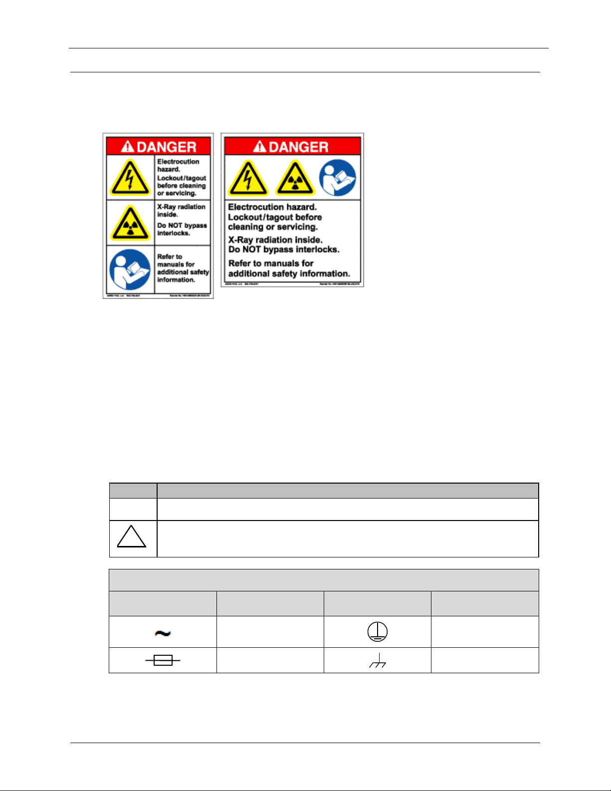
Safety Compliance
Examples of Multi-Hazard Formats
EN 60950
Applicable testing is routinely performed as a condition of manufacturing on all units to ensure
compliance with the requirements of the EN 60950 Safety of Information Technology
Equipment (Including Electrical Business Machines) safety standard.
This equipment meets the Safety of Information Technology Equipment specification as defined
in EN60950.
Low Voltage Directive (LVD)
The following information is applicable for the European Low Voltage Directive (2006/95/EC):
Symbol Description
<HAR>
!
Type of power cord required for use in the European Community.
CAUTION: Double-pole/Neutral Fusing
ACHTUNG: Zweipolige bzw. Neutralleiter-Sicherung
Symbol Definition Symbol Definition
International Symbols
MN-DMDREMOTEOP Revision 9 vi
Alternating Current
Fuse
Protective Earth
Chassis Ground
Page 9

DMD20/DMD50/DMD2050/DMD2050E/DMD1050/OM20 Remote Protocol Preface
Warranty Policy
Comtech EF Data products are warranted against defects in material and workmanship for a specific period from the date of shipment, and
this period varies by product. In most cases, the warranty period is two years. During the warranty period, Comtech EF Data will, at its
option, repair or replace products that prove to be defective. Repairs are warranted for the remainder of the original warranty or a 90 day
extended warranty, whichever is longer. Contact Comtech EF Data for the warranty period specific to the product purchased.
For equipment under warranty, the owner is responsible for freight to Comtech EF Data and all related customs, taxes, tariffs, insurance,
etc. Comtech EF Data is responsible for the freight charges only for return of the equipment from the factory to the owner. Comtech EF
Data will return the equipment by the same method (i.e., Air, Express, Surface) as the equipment was sent to Comtech EF Data.
All equipment returned for warranty repair must have a valid RMA number issued prior to return and be marked clearly on the return
packaging. Comtech EF Data strongly recommends all equipment be returned in its original packaging.
Comtech EF Data Corporation’s obligations under this warranty are limited to repair or replacement of failed parts, and the return shipment
to the buyer of the repaired or replaced parts.
Limitations of Warranty
The warranty does not apply to any part of a product that has been installed, altered, repaired, or misused in any way that, in the opinion of
Comtech EF Data Corporation, would affect the reliability or detracts from the performance of any part of the product, or is damaged as the
result of use in a way or with equipment that had not been previously approved by Comtech EF Data Corporation.
The warranty does not apply to any product or parts thereof where the serial number or the serial number of any of its parts has been
altered, defaced, or removed.
The warranty does not cover damage or loss incurred in transportation of the product.
The warranty does not cover replacement or repair necessitated by loss or damage from any cause beyond the control of Comtech EF
Data Corporation, such as lightning or other natural and weather related events or wartime environments.
The warranty does not cover any labor involved in the removal and or reinstallation of warranted equipment or parts on site, or any labor
required to diagnose the necessity for repair or replacement.
The warranty excludes any responsibility by Comtech EF Data Corporation for incidental or consequential damages arising from the use of
the equipment or products, or for any inability to use them either separate from or in combination with any other equipment or products.
A fixed charge established for each product will be imposed for all equipment returned for warranty repair where Comtech EF Data
Corporation cannot identify the cause of the reported failure.
Exclusive Remedies
Comtech EF Data Corporation’s warranty, as stated is in lieu of all other warranties, expressed, implied, or statutory, including those of
merchantability and fitness for a particular purpose. The buyer shall pass on to any purchaser, lessee, or other user of Comtech EF Data
Corporation’s products, the aforementioned warranty, and shall indemnify and hold harmless Comtech EF Data Corporation from any
claims or liability of such purchaser, lessee, or user based upon allegations that the buyer, its agents, or employees have made additional
warranties or representations as to product preference or use.
The remedies provided herein are the buyer’s sole and exclusive remedies. Comtech EF Data shall not be liable for any direct, indirect,
special, incidental, or consequential damages, whether based on contract, tort, or any other legal theory.
MN-DMDREMOTEOP Revision 9 vii
Page 10

DMD20/DMD50/DMD2050/DMD2050E/DMD1050/OM20 Remote Protocol Preface
Comtech EF Data Headquarters
http://www.comtechefdata.com
Comtech EF Data Corp.
2114 West 7
Tempe, Arizona USA 85281
+1.480.333.2200
th
Street
MN-DMDREMOTEOP Revision 9 viii
Page 11

Chapter 1. Remote Operations
1.1 Introduction
The Remote Protocols for the DMD20, DMD20LBST, DMD50, DMD2050, DMD2050E,
DMD1050 and OM20 are similar in design and utilize the same protocol platforms. This
document should be used as the primary source for identifying the various protocol structures
and control menus for products listed below. The most current Remote Protocols manual can be
accessed from the Radyne web site at http://www.comtechefdata.com
The Remote Protocols identified in MN-DMDREMOTEOP are RLLP (Radyne Link Level
Protocol), SNMP MIB file, Web Browser menus and Terminal Port menus. The MNDMDREMOTEOP document does not identify equipment setup processes. The Product manuals
include instructions to set up the equipment but will not include the protocol structure. The
Remote Protocol manual MN-DMDREMOTEOP is applicable to the following products:
Equipment Manual
DMD20 MN-DMD20/20LBST
DMD20LBST MN-DMD20/20LBST
DMD50 MN-DMD50
DMD2050 MN-DMD2050
DMD2050E MN-DMD2050E
DMD1050 MN-DMD1050
OM20 MN-OM20
1.2 Modem Remote Communications (RLLP):
The Remote Port allows for complete control and monitoring of all parameters and functions via
an RS-232 Serial Interface or RS-485 for RLLP Protocol. ‘Equipment Remote Mode’ can be
entered from the GUI interface under the “System” menu by selecting “System” and then
“Terminal” followed by “Terminal”. The baud rate and evaluation type can be changed at the front
panel by using the System>Baud Rate Menu.
Control and status messages are conveyed between the modem and all subsidiary modems and
the host computer using packetized message blocks in accordance with a proprietary
communications specification. This communication is handled by the Radyne Link Level Protocol
(RLLP), which serves as a protocol ‘wrapper’ for the RM&C data. Complete information on
monitor and control software is contained in the following sections.
MN-DMDREMOTEOP Revision 9 1–1
Page 12

DMD20/DMD50/DMD2050/DMD2050E/DMD1050/OM20 Remote Protocol Remote Operations
This specification is applicable to the DMD20/20LBST, DMD50, DMD2050,
DMD2050E, DMD1050 and OM20 Modems. Any reference to the DMD20 in this
document can be applicable to any one of these three modems.
For configuration setup, refer to the product manuals.
1.2.1 Protocol Structure:
The Communications Specification (COMMSPEC) defines the interaction of computer resident
Monitor and Control Software used in satellite earth station equipment such as modems,
redundancy switches, multiplexers, and other ancillary support gear. Communication is bidirectional, and is normally established on one or more full-duplex 9600-baud multi-drop control
buses that conform to EIA Standard RS-485.
Each piece of earth station equipment on a control bus has a unique physical address, which is
assigned during station se tup/config uration or prior to ship ment. Valid dec imal addr esses on one
control bus range from 032 through 255 for a total of up to 224 devices per bus. Address 255 of
each control bus is usually reserved for the M&C computer.
1.2.2 Protocol Wrapper:
The Radyne COMMSPEC is byte-oriented, with the Least Significant Bit (LSB) issued first. Each
data byte is conveyed as mark/space information with two marks comprising the stop data. When
the last byte of data is transmitted, a hold comprises one steady mark (the last stop bit). To begin
or resume data transfer, a space (00h) substitutes this mark. This handling scheme is controlled
by the hardware and is transparent to the user. A pictorial representation of the data and its
surrounding overhead may be shown as follows:
S1 S2 B
0
The Stop Bits, S1 and S2, are each a mark. Data flow remains in a hold mode until S2 is
replaced by a space. If S2 is followed by a space, it is considered a start bit for the data byte and
not part of the actual data (B
Level Protocol (RLLP) organizes the actual monitor and control data within a shell, or ‘protocol
wrapper’ that surrounds the data. The format and structure of the COMMSPEC message
exchanges are described herein. Decimal numbers have no suffix; hexadecimal numbers end
with a lower case ‘h’ suffix and binary values have a lower case ‘b’ suffix. Thus, 22 = 16h =
000010110b. The principal elements of a data frame, in order of occurrence, are summariz ed as
follows:
<SYNC>: The message format header character or ASCII sync character that defines the
beginning of a message. The <SYNC> character value is always 16h.
<BYTE COUNT>: The Byte Count is the number of bytes in the <DATA> field (2 Bytes).
<SOURCE ID>: The Source Identifier defines the multi-drop addres s origin.
B1 B2 B3 B4 B5 B6 B7 S1 S2, etc.
0
- B 7). The COMMSPEC developed for use with the Radyne Link
MN-DMDREMOTEOP Revision 9 1–2
Page 13

DMD20/DMD50/DMD2050/DMD2050E/DMD1050/OM20 Remote Protocol Remote Operations
All nodes on a given control bus have a unique address that must be defined.
<DESTINATION ID>: The Destination Identifier serves as a pointer to the multi-drop destination
device that indicates where the message is to be sent.
<FRAME SEQUENCE NUMBER>: The Frame Sequence Number (FSN) is a tag with a value
from 0 through 255 that is sent with each message. It assures sequential information
framing and correct equipment acknowledgment and data transfers.
<OPCODE>: The Operation Code field contains a number that identifies the message type
associated with the data that follows it. Equipment under MCS control recognizes this
byte via firmware identification and subsequently steers the DATA accordingly to perform
a specific function or series of functions. Acknowledgment and error codes are returned
in this field (2 Bytes).
<DATA>: The Data field contains the binary, bi-directional data bytes associated with the
<OPCODE>. The number of data bytes in this field is indicated by the <BYTE COUNT>
value.
<CHECKSUM>: The checksum is the modulo 256 sum of all preceding message bytes,
excluding the <SYNC> character. The checksum determines the presence or absence of
errors within the message. In a message block with the following parameters, the
checksum is computed as shown in Table 1-1.
BYTE FIELD DATA CONTENT RUNNING CHECKSUM
<BYTE COUNT> (BYTE 1) 00h = 00000000b 00000000b
<BYTE COUNT> (BYTE 2) 04h = 00000100b 00000100b
<SOURCE ID> FFh = 11111111b 00000011b
<DESTINATION ID> 20h = 00100000b 00100011b
<FSN> 09h = 00001001b 00101100b
<OPCODE> (BYTE 1) 2Ah = 00101010b 01010110b
<OPCODE> (BYTE 2) 01h = 00000001b 01010111b
<DATA> (Byte 1) 08h = 00001000b 01011111b
<DATA> (Byte 2) 58h = 01011000b 10110111b
<DATA> (Byte 3) 3Bh = 00111011b 11110010b
<DATA> (Byte 4) 00h = 00000000b 11110010b
Table 1-1: Checksum Calculation Example
Thus, the checksum is 11110010b; which is F2h or 242 decimal. Alternative methods of
calculating the checksum for the same message frame are:
00h + 04h + FFh + 20h + 09h + 2Ah + 01h + 08h + 58h + 3Bh + 00h = 1 F 2h.
Since the only concern is the modulo 256 (modulo 1 00h) equivalent (values that can be
represented by a single 8-bit byte), the checksum is F2h. For a decimal checksum calculation, the
equivalent values for each information field are:
0 + 4 + 255 + 32 + 9 + 42 + 1 + 8 + 88 + 59 + 0 = 498;
498/256 = 1 with a remainder of 242.
MN-DMDREMOTEOP Revision 9 1–3
Page 14

DMD20/DMD50/DMD2050/DMD2050E/DMD1050/OM20 Remote Protocol Remote Operations
This remainder is the checksum for the frame.
242 (decimal) = F2h = 11110010b = <CHECKSUM>
1.2.3 Frame Description and Bus Handshaking:
In a Monitor and Control environment, every message frame on a control bus port executes as a
packet in a loop beginning with a wait-for-SYNC-character mode. The remaining message format
header information is then loaded, either by the M&C computer or by a subordinate piece of
equipment (such as the DMD20) requesting access to the bus. Data is processed in accordance
with the OPCODE, and the checksum for the frame is calculated. If the anticipated checksum
does not match, then a checksum error response is returned to the message frame originator.
The entire message frame is discarded and the wait-for-SYNC mode goes back into effect. If the
OPCODE resides within a command message, it defines the class of action that denotes an
instruction that is specific to the device type, and is a prefix to the DATA field if data is required. If
the OPCODE resides within a query message packet, then it defines the query code, and can
serve as a prefix to query code DATA.
The Frame Sequence Number (FSN) is included in every message packet and increments
sequentially. When the M&C computer or bus-linked equipment initiates a message, it assigns
the FSN as a tag for error control and handshaking. A different FSN is produced for each new
message from the FSN originator to a specific device on the control bus. If a command packet is
sent and not received at its intended destination, then an appropriate response message is not
received by the packet originator. The original command packet is then re-transmitted with the
same FSN. If the repeated message is received correctly at this point, it is considered a new
message and is executed and acknowledged as such.
If the command packet is received at its intended destination but the response message
(acknowledgment) is lost, then the message originator (usually the M&C computer) re-transmits
the original command packet with the same FSN. The destination device detects the same FSN
and recognizes that the message is a duplicate, so the associated commands within the packet
are not executed a second time. However, the response packet is again sent back to the source
as an acknowledgment in order to preclude undesired multiple executions of the same
command.
To reiterate, valid equipment responses to a message require the FSN tag in the command
packet. This serves as part of the handshake/acknowledges routine. If a valid response message
is absent, then the command is re-transmitted with the same FSN. For a repeat of the same
command involving iterative processes (such as increasing or decreasing the transmit power
level of a DMD20 modulator), the FSN is incremented after each message packet. When the
FSN value reaches 255, it overflows and begins again at zero. The FSN tag is a powerful tool
that assures sequential information framing, and is especially useful where commands require
more than one message packet.
The full handshake/acknowledgment involves a reversal of source and destination ID codes in
the next message frame, followed by a response code in the <OPCODE> field of the message
packet from the equipment under control.
If a command packet is sent and not received at its intended destination, a timeout condition can
occur because a response message is not received by the packet originator. On receiving
devices slaved to an M&C computer, the timeout delay parameters may be programmed into the
equipment in accordance with site requirements by Radyne prior to shipment, or altered by
qualified personnel. The FSN handshake routines must account for timeout delays and be able
to introduce them as well.
MN-DMDREMOTEOP Revision 9 1–4
Page 15
DMD20/DMD50/DMD2050/DMD2050E/DMD1050/OM20 Remote Protocol Remote Operations
1.2.4 Global Response Operational Codes:
In acknowledgment (response) packets, the operational code <OPCODE> field of the message
packet is set to 0 by the receiving devices when the message intended for the device is
evaluated as valid. The device that receives the valid message then exchanges the <SOURCE
ID> with the <DESTINATION ID>, sets the <OPCODE> to zero in order to indicate that a good
message was received, and returns the packet to the originator. This "GOOD MESSAGE"
Opcode is one of nine global responses. Global response opcodes are common responses,
issued to the M&C computer or to another device that can originate from and are interpreted by
all Radyne equipment in the same manner. These are summarized as follows (all opcode values
are expressed in decimal form):
Response OPCODE Description OPCODE
Good Message 000d = 0000h
Bad Parameter 255d = 00FFh
Bad Opcode 254d = 00FEh
Incomplete Parameter 247d = 00F7h
Table 1-2: Response OPCODES
The following response error codes are specific to the DMD20:
DMD20 Response Error Code Descriptions OPCODE
MPARM_FREQUENCY_ERROR 0x0401
MPARM_STRAP_ERROR 0x0402
MPARM_FILTERMASK_ERROR 0x0403
MPARM_DATARATE_ERROR 0x0404
MPARM_EXTEXCCLOCK_ERROR 0x0405
MPARM_EXTREFERENCE_ERROR 0x0406
MPARM_EXTREFSOURCE_ERROR 0x0407
MPARM_MODULATIONTYPE_ERROR 0x0408
MPARM_CONVENCODER_ERROR 0x0409
MPARM_REEDSOLOMON_ERROR 0x040A
MPARM_SCRAMBLERCONTROL_ERROR 0x040B
MPARM_SCRAMBLERTYPE_ERROR 0x040C
MPARM_DIFFERENTIALENCODER_ERROR 0x040F
MPARM_XMITPOWERLEVEL_ERROR 0x0410
MPARM_CARRIERCONTROL_ERROR 0x0411
MPARM_CARRIERSELECTION_ERROR 0x0412
MPARM_SPECTRUM_ERROR 0x0413
MPARM_TXTESTPATTERN_ERROR 0x0414
MPARM_TERRLOOPBACK_ERROR 0x0415
MPARM_BASELOOPBACK_ERROR 0x0416
MPARM_CLOCKCONTROL_ERROR 0x0417
MPARM_CLOCKPOLARITY_ERROR 0x0418
MPARM_FRAMING_ERROR 0x0419
MPARM_DROPMODE_ERROR 0x041A
MPARM_SCTSOURCE_ERROR 0x041B
MPARM_T1D4YELLOW_ERROR 0x041E
MPARM_NETWORKSPEC_ERROR 0x0422
MPARM_CIRCUITID_ERROR 0x0423
MPARM_ESCCHANNEL1VOLUME_ERROR 0x0424
MPARM_ESCCHANNEL2VOLUME_ERROR 0x0425
MPARM_INTERFACETYPE_ERROR 0x0429
MPARM_INTERFACENOTPRESENT_ERROR 0x042A
MN-DMDREMOTEOP Revision 9 1–5
Page 16

DMD20/DMD50/DMD2050/DMD2050E/DMD1050/OM20 Remote Protocol Remote Operations
MPARM_INTERFACECOMMUNICATION_ERROR 0x042B
MPARM_SYMBOLRATE_ERROR 0x042C
MPARM_NOTIMPLEMENTED_ERROR 0x042D
MPARM_SUMMARYFAULT_ERROR 0x0430
MPARM_DATAINVERT_ERROR 0x0431
MPARM_ESCSOURCE_ERROR 0x0432
MPARM_AUPCLOCALENABLE_ERROR 0x0435
MPARM_AUPCREMOTEENABL_ERROR 0x0436
MPARM_AUPCLOCALCLACTION_ERROR 0x0437
MPARM_AUPCREMOTECLACTION_ERROR 0x0438
MPARM_AUPCTRACKINGRATE_ERROR 0x0439
MPARM_AUPCREMOTEBBLOOPACK_ERROR 0x043A
MPARM_AUPCREMOTE2047_ERROR 0x043B
MPARM_AUPCEBNO_ERROR 0x043C
MPARM_AUPCMINPOWER_ERROR 0x043D
MPARM_AUPCMAXPOWER_ERROR 0x043E
MPARM_AUPCNOMINAPOWER_ERROR 0x043F
MPARM_ASYNCBAUDRATE_ERROR 0x0452
MPARM_ASYNCDATABITS_ERROR 0x0453
MPARM_ASYNCMODE_ERROR 0x0454
MPARM_TPCINTERLEAVER_ERROR 0x0455
DPARM_NETWORKSPEC_ERROR 0x0600
DPARM_FREQUENCY_ERROR 0x0601
DPARM_SWEEPDELAY_ERROR 0x0602
DPARM_DATARATE_ERROR 0x0603
DPARM_SWEEPBOUNDARY_ERROR 0x0604
DPARM_LEVELLIMIT_ERROR 0x0605
DPARM_STRAP_ERROR 0x0606
DPARM_FILTERMASK_ERROR 0x0607
DPARM_DEMODULATIONTYPE_ERROR 0x0608
DPARM_CONVDECODER_ERROR 0x0609
DPARM_REEDSOLOMON_ERROR 0x060A
DPARM_DIFFERENTIALDECODER_ERROR 0x060B
DPARM_DESCRAMBLERCONTROL_ERROR 0x060C
DPARM_DESCRAMBLERTYPE_ERROR 0x060D
DPARM_SPECTRUM_ERROR 0x060E
DPARM_BUFFERSIZE_ERROR 0x060F
DPARM_BUFFERCLOCK_ERROR 0x0610
DPARM_BUFFERCLOCKPOL_ERROR 0x0611
DPARM_INSERTMODE_ERROR 0x0612
DPARM_T1E1FRAMESOURCE_ERROR 0x0614
DPARM_FRAMING_ERROR 0x0615
DPARM_RXTESTPATTERN_ERROR 0x0616
DPARM_MAPSUMMARY_ERROR 0x0617
DPARM_BEREXPONENT_ERROR 0x0619
DPARM_CIRCUITID_ERROR 0x061A
DPARM_TERRLOOPBACK_ERROR 0x061B
DPARM_BASELOOPBACK_ERROR 0x061C
DPARM_IFLOOPBACK_ERROR 0x061D
DPARM_INTERFACETYPE_ERROR 0x061E
DPARM_INTERFACENOTPRESENT_ERROR 0x061F
DPARM_INTERFACECOMMUNICATION_ERROR 0x0620
DPARM_SYMBOLRATE_ERROR 0x0621
MN-DMDREMOTEOP Revision 9 1–6
Page 17

DMD20/DMD50/DMD2050/DMD2050E/DMD1050/OM20 Remote Protocol Remote Operations
DPARM_NOTIMPLEMENTED_ERROR 0x0622
DPARM_DATAINVERT_ERROR 0x0623
DPARM_SUMMARYFAULT_ERROR 0x0624
DPARM_EXTERNALEXCSOURCE_ERROR 0x0625
DPARM_ASYNCMODE_ERROR 0x062C
DPARM_ASYNCBAUDRATE_ERROR 0x062D
DPARM_ASYNCTYPE_ERROR 0x062E
DPARM_ASYNCDATABITS_ERROR 0x062F
DPARM_REACQ_SWEEP_ERROR 0x0631
DPARM_ESCCHANNEL1VOLUME_ERROR 0x0632
DPARM_ESCCHANNEL2VOLUME_ERROR 0x0633
DPARM_ESCOVERHEADTYPE_ERROR 0x0634
DPARM_TPCINTERLEAVER_ERROR 0x0635
DPARM_FASTACQENABLE_ERROR 0x0636
DPARM_RFMTIMECONSTANT_ERROR 0x0637
MDPARM_MAPNUMBER_ERROR 0x0A00
MDPARM_TIME_ERROR 0x0A01
MDPARM_DATE_ERROR 0x0A02
MDPARM_MINORALARMRELAYUSAGE_ERROR 0x0A03
1.2.5 Collision Avoidance:
When properly implemented, the physical and logical devices and ID addressing scheme of the
COMMSPEC normally precludes message packet contention on the control bus. The importance
of designating unique IDs for each device during station configuration cannot be
overemphasized. One pitfall, which is often overlooked, concerns multi-drop override IDs. All too
often, multiple devices of the same type are assigned in a direct-linked ("single-thread")
configuration accessible to the M&C computer directly.
For example, if two DMD20 Modems with different addresses (DESTINATION IDs) are linked to
the same control bus at the same hierarchical level, both will attempt to respond to the M&C
computer when the computer generates a multi-drop override ID of 22. If their actual setup
parameters, status, or internal timing differs, they will both attempt to respond to the override
simultaneously with different information or asynchronously in their respective message packets
and response packets, causing a collision on the serial control bus.
To preclude control bus data contention, different IDs must always be assigned to the
equipment. If two or more devices are configured for direct-linked operation, then the M&C
computer and all other devices configured in the same manner must be programmed to inhibit
broadcast of the corresponding multi-drop override ID.
The multi-drop override ID is always accepted by devices of the same type on a common control
bus, independent of the actual DESTINATION ID. These override IDs with the exception of
“BROADCAST” are responded to by all directly linked devices of the same type causing
contention on the bus. The “BROADCAST” ID, on the other hand, is accepted by all equipment
but none of then returns a response packet to the remote M&C.
The following multi-drop override IDs are device-type specific, with the exception of
"BROADCAST". These are summarized below with ID values expressed in decimal notation:
Directly-Addressed Equipment Multi-Drop Override ID
Broadcast (all directly-linked devices) 00
DMD-3000/4000, 4500 or 5000 Mod Section, DMD20 01
DMD-3000/4000, 4500 or 5000 Demod Section, DMD20 02
MN-DMDREMOTEOP Revision 9 1–7
Page 18
DMD20/DMD50/DMD2050/DMD2050E/DMD1050/OM20 Remote Protocol Remote Operations
RCU-340 1:1 Switch 03
RCS-780 1:N Switch 04
RMUX-340 Cross-Connect Multiplexer 05
CDS-780 Clock Distribution System 06
SOM-340 Second Order Multiplexer 07
DMD-4500/5000 Modulator Section 08
DMD-4500/5000 Demodulator Section 09
RCU-5000 M:N Switch 10
DMD20 Modulator 20
DMD20 Demodulator 21
DMD20 Modem 22
DVB3030 Video Modulator, DM240 23
RCS20 M:N Switch 24
RCS10 M:N Switch 25
RCS11 1:1 Switch 26
Reserved for future equipment types 27-31
Multi-drop override IDs 01 or 02 can be used interchangeably to broadcast a
message to a DMD-3000/4000 Modem, DMD-4500/5000, or a DMD20 Modem.
Radyne recommends that the multi-drop override IDs be issued only during
system configuration as a bus test tool by experienced programmers and that
they not be included in run-time software. It is also advantageous to consider
the use of multiple bus systems where warranted by a moderate to large
equipment complement.
Therefore, if a DMD20 Modulator is queried for its equipment type identifier, it will return a "20"
and DMD20 Demodulator will return a "21". A DMD20 Modem will also return a "22".
1.2.6 Software Compatibility:
The COMMSPEC, operating in conjunction within the RLLP shell, provides for full forward and
backward software compatibility independent of the software version in use. New features are
appended to the end of the DATA field without OPCODE changes. Older software simply
discards the data as extraneous information without functional impairment for backward
compatibility.
If new device-resident or M&C software receives a message related to an old software version,
new information and processes are not damaged or affected by the omission of data.
The implementation of forward and backward software compatibility often, but not always,
requires the addition of new Opcodes. Each new function requires a new Opcode assignment if
forward and backward compatibility cannot be attained by other means.
When Radyne equipment is queried for bulk information (Query Mod, Query Demod, etc.) it
responds by sending back two blocks of data; a Non-Volatile Section (parameters that can be
modified by the user) and a Volatile Section (status information). It also returns a count value that
indicates the size of the Non-Volatile Section. This count is used by M&C developers to index
into the start of the Volatile Section.
When new features are added to Radyne equipment, the control parameters are appended to
the end of the Non-Volatile Section, and status of the features, if any, are added at the end of the
MN-DMDREMOTEOP Revision 9 1–8
Page 19

DMD20/DMD50/DMD2050/DMD2050E/DMD1050/OM20 Remote Protocol Remote Operations
Volatile Section. If a remote M&C queries two pieces of Radyne equipment with different revision
software, they may respond with two different sized packets. The remote M&C MUST make use
of the non-volatile count value to index to the start of the Volatile Section. If the remote M&C is
not aware of the newly added features to the Radyne product, it should disregard the parameters
at the end of the Non-Volatile Section and index to the start of the Volatile Section.
If packets are handled in this fashion, there will also be backward-compatibility between Radyne
equipment and M&C systems. Remote M&C systems need not be modified every time a feature
is added unless the user needs access to that feature.
1.2.7 Flow Control and Task Processing:
The original packet sender (the M&C computer) relies on accurate timeout information with
regard to each piece of equipment under its control. This provides for efficient bus
communication without unnecessary handshake overhead timing. One critical value is
designated the Inter-Frame Space (FS). The Inter-Frame Space provides a period of time in
which the packet receiver and medium (control bus and M&C computer interface) fully recover
from the packet transmission/reception process and the receiver is ready to accept a new
message. The programmed value of the Inter-Frame Space should be greater than the sum of
the "turnaround time" and the round-trip (sender/receiver/bus) propagation time, including
handshake overhead. The term "turnaround time" refers to the amount of time required for a
receiver to be re-enabled and ready to receive a packet after having just received a packet. In
flow control programming, the Inter-Frame Space may be determined empirically in accord with
the system configuration or calculated based on established maximum equipment task
processing times.
Each piece of supported equipment on the control bus executes a Radyne Link Level Task
(RLLT) in accordance with its internal hardware and fixed program structure. In a flow control
example, the RLLT issues an internal "message in" system call to invoke an I/O wait condition
that persists until the task receives a command from the M & C computer. The RLLT has the
option of setting a timeout on the incoming message. Thus, if the equipment does not receive an
information/command packet within a given time period, the associated RLLT exits the I/O wait
state and takes appropriate action.
Radyne equipment is logically linked to the control bus via an Internal I/O Processing Task
(IOPT) to handle frame sequencing, error checking, and handshaking. The IOPT is essentially a
link between the equipment RLLT and the control bus. Each time the M&C computer sends a
message packet; the IOPT receives the message and performs error checking. If errors are
absent, the IOPT passes the message to the equipment's RLLT. If the IOPT detects errors, it
appends error messages to the packet. Whenever an error occurs, the IOPT notes it and
discards the message; but it keeps track of the incoming packet. Once the packet is complete,
the IOPT conveys the appropriate message to the RLLT and invokes an I/O wait state (wait for
next <SYNC> character).
If the RLLT receives the packetized message from the sender before it times out, it checks for
any error messages appended by the IOPT. In the absence of errors, the RLLT processes the
received command sent via the transmitted packet and issues a "message out" system call to
ultimately acknowledge the received packet. This call generates the response packet conveyed
to the sender. If the IOPT sensed errors in the received packet and an RLLT timeout has not
occurred, the RLLT causes the equipment to issue the appropriate error message(s) in the
pending equipment response frame.
MN-DMDREMOTEOP Revision 9 1–9
Page 20

DMD20/DMD50/DMD2050/DMD2050E/DMD1050/OM20 Remote Protocol Remote Operations
To maintain frame synchronization, the IOPT keeps track of error-laden packets and packets
intended for other equipment for the duration of each received packet. Once the packet is
complete, the IOPT invokes an I/O wait state and searches for the next <SYNC> character.
1.2.8 RLLP Summary:
The RLLP is a simple send-and-wait protocol that automatically re-transmits a packet whenever
an error is detected, or when an acknowledgment (response) packet is absent.
During transmission, the protocol wrapper surrounds the ac tual data to form information packets.
Each transmitted packet is subject to time out and frame sequence control parameters, after
which the packet sender waits for the receiver to convey its response. Once a receiver verifies
that a packet sent to it is in the correct sequence relative to the previously received packet, it
computes a local checksum on all information within the packet excluding the <SYNC> character
and the <CHECKSUM> fields. If this checksum matches the packet <CHECKSUM>, the receiver
processes the packet and responds to the packet sender with a valid response
(acknowledgment) packet. If the checksum values do not match, the receiver replies with a
negative acknowledgment (NAK) in its response frame.
The response packet is therefore an acknowledgment either that the message was received
correctly, or some form of a packetized NAK frame. If the sender receives a valid
acknowledgment (response) packet from the receiver, the <FSN> increments and the next
packet is transmitted as required by the sender. However, if a NAK response packet is returned
the sender re-transmits the original information packet with the same embedded <FSN>.
If an acknowledgment (response) packet or a NAK packet is lost, corrupted, or not issued due to
an error and is thereby not returned to the sender, the sender re-transmits the original
information packet; but with the same <FSN>. When the intended receiver detects a duplicate
packet, the packet is acknowledged with a response packet and internally discarded to preclude
undesired repetitive executions. If the M&C computer sends a command packet and the
corresponding response packet is lost due to a system or internal error, the computer times out
and re-transmits the same command packet with the same <FSN> to the same receiver and
waits once again for an acknowledgment or a NAK packet.
To reiterate, the format of the Link Level Protocol Message Block is shown below.
SYNC
Byte
Byte
COUNT
SOURCE
ADDRESS
DESTINATION
ADDRESS
FSN OPCODE
DATA
BYTES
CHECKSUM
1.3 Remote Port Packet Structure:
The Modem protocol is an enhancement on the DMD20 protocol. It also uses a packet structure
format. The structure is as follows:
<SYNC>: Message format header character that defines the beginning of a message. The
<SYNC> character value is always 0x16 (1 byte).
<BYTE COUNT>: The number of bytes in the <DATA> field (2 bytes).
<SOURCE ID>: Identifies the address of the equipment from where the message originated (1
byte).
<DESTINATION ID>: Identifies the address of the equipment where the message is to be sent (1
byte).
MN-DMDREMOTEOP Revision 9 1–10
Page 21
DMD20/DMD50/DMD2050/DMD2050E/DMD1050/OM20 Remote Protocol Remote Operations
<FSN>: Frame sequence number ensures correct packet acknowledgment and data transfers (1
byte).
<OPCODE>: This byte identifies the message type associated with the information data. The
equipment processes the data according to the value in this field. Return error codes and
acknowledgment are also included in this field (2 bytes).
<...DATA...>: Information data. The number of data bytes in this field is indicated by the <BYTE
COUNT> value.
<CHECKSUM>: The modulo 256 sum of all preceding message bytes excluding the <SYNC>
character (1 byte).
The Modem RLLP is not software-compatible with the following previous
Radyne products: RCU5000 and DMD4500. These products may not occupy the
same bus while using this protocol as equipment malfunction and loss of data
may occur.
When transmitting a packet at 9600 baud, the Remote M&C should ensure that
the timeout value between characters does not exceed the time it takes to
transmit 200 characters (≈
200 msec). If this timeout value is exceeded, the
equipment will timeout.
1.4 DMD20 Opcode Command Set:
The DMD20/DMD20 LBST Opcode Command Set is listed below:
MN-DMDREMOTEOP Revision 9 1–11
Page 22

DMD20/DMD50/DMD2050/DMD2050E/DMD1050/OM20 Remote Protocol Remote Operations
When new features are added to Radyne equipment, the control parameters
are appended to the end of the Non-Volatile Section of the Remote
Communications Specification, and status of the features, if any, are added at
the end of the Volatile Section. If a remote M & C queries two pieces of Radyne
equipment with different revision software, they could respond with two
different sized packets. The remote M & C MUST make use of the non-volatile
count value to index to the start of the Volatile Section. If the remote M & C is
not aware of the newly added features to the product, it should disregard the
parameters at the end of the Non-Volatile Section and index to the start of the
Volatile Section.
Before creating any software based on the information contained in this
document, contact the Comtech EF Data Customer Service Department (480333-4357) to find out if the software revision for that piece of equipment is
current and that no new features have been added since the release of this
document.
1.4.1 Modem Command Set:
Query Modulator Configuration and Status 2400h
Query Demodulator Configuration and Status 2401h
Query Modem Drop & Insert Map 2402h
Query Modems Identification 2403h
Query Modem Control Mode 2404h
Query Modulator Latched Alarms 2405h
Query Demodulator Latched Alarms 2406h
Query Modem Latched Alarms 2407h
Query Modulator Current Alarms 2408h
Query Demodulator Current Alarms 2409h
Query Modem Current Alarms 240Ah
Query Modulator Status 240Bh
Query Demodulator Status 240Ch
Query Modem Eb/No, BER and Level 240Dh
Query Time 240Eh
Query Date 240Fh
Query Time and Date 2410h
Query Modem Summary Faults 2411h
Query Modem Event Buffer 2412h
Query Modulator Configuration 2448h
Query Demodulator Configuration 2449h
Query Modem Features 2450h
Query Modulator Async Configuration 2451h
Query Demodulator Async Configuration 2452h
Query Up converter Configuration 2490h
Query Uplink RF 2491h
Query Down converter Configuration 2492h
Query Downlink RF 2493h
Query Demodulator Ethernet Terrestrial Interface Packet Status 2494h
Command Opcode
MN-DMDREMOTEOP Revision 9 1–12
Page 23

DMD20/DMD50/DMD2050/DMD2050E/DMD1050/OM20 Remote Protocol Remote Operations
Query CNC Status 2495h
Query BUC FSK Pass Thru Reply 2E06h
Command Opcode
Command Up converter Configuration 2500h
Command Uplink RF 2501h
Command Down converter Configuration 2502h
Command Downlink RF 2503h
Command Modem Control Mode 2600h
Command Modulator Configuration 2601h
Command Modulator Frequency 2602h
Command Modulator Strap Code 2603h
Command Modulator Data Rate 2604h
Command Modulator Filter Mask 2605h
Command Modulator Modulation Type 2606h
Command Modulator Convolutional Encoder 2607h
Command Modulator Differential Encoder 2608h
Command Modulator Carrier Control 2609h
Command Modulator Carrier Selection 260Ah
Command Modulator Clock Control 260Bh
Command Modulator Clock Polarity 260Ch
Command Modulator SCT Source 260Dh
Command Modulator Drop Mode 260Eh
Command Modulator Output Level 260Fh
Command Modulator Reed Solomon 2610h
Command Modulator Spectrum 2611h
Command Modulator Test Pattern 2612h
Command Modulator Scrambler Control 2613h
Command Modulator Scrambler Type 2614h
Command Modulator Framing 2615h
Command Modulator External Reference Source 2616h
Command Modulator Terrestrial Loopback 2617h
Command Modulator Baseband Loopback 2618h
Command Modulator Network Spec 2619h
Command Modulator External EXC Clock 261Ah
Command Modulator External Reference Frequency 261Bh
Command Modulator T1 D4 Yellow Alarm Selection 261Dh
Command Modulator Interface Type 261Eh
Command Modulator Circuit ID 261Fh
Command Force Modulator Alarm Test 2622h
Command Modulator Data Invert 2623h
Clear Modulator Latched Alarm 1 2625h
Command AUPC Local Enable 2629h
Command AUPC Remote Enable 262Ah
Command AUPC Local CL Action 262Bh
Command AUPC Remote CL Action 262Ch
Command AUPC Tracking Rate 262Dh
Command AUPC Remote BB Loopback 262Eh
Command AUPC Remote Test 2047 262Fh
Command AUPC Eb/No 2630h
Command AUPC Minimum Power 2631h
Command AUPC Maximum Power 2632h
Command AUPC Nominal Power 2633h
MN-DMDREMOTEOP Revision 9 1–13
Page 24

DMD20/DMD50/DMD2050/DMD2050E/DMD1050/OM20 Remote Protocol Remote Operations
Command AUPC Local Configuration 2634h
Command AUPC Remote Configuration 2635h
Command Modulator Reed Solomon N & K Codes and Interleaver Depth 2636h
Command Modulator TPC Interleaver 2638h
Command Modulator Async Configuration 2640h
Command Minor Alarm Relay Usage 2641h
Command Modulator Ethernet Terrestrial Interface Configuration 2642h
Command Demodulator Configuration 2A00h
Command Demodulator Frequency 2A01h
Command Demodulator Data Rate 2A02h
Command Demodulator Strap Code 2A03h
Command Demodulator Sweep Boundary 2A04h
Command Demodulator Sweep Delay 2A05h
Command Demodulator Demodulation Type 2A07h
Command Demodulator Convolutional Decoder 2A08h
Command Demodulator Differential Decoder 2A09h
Command Demodulator Reed Solomon 2A0Ah
Command Demodulator Network Spec 2A0Bh
Command Demodulator Filter Mask 2A0Ch
Command Demodulator Descrambler Control 2A0Dh
Command Demodulator Descrambler Type 2A0Eh
Command Demodulator Spectrum 2A0Fh
Command Demodulator Buffer Size 2A10h
Command Demodulator Buffer Clock 2A11h
Command Demodulator Buffer Clock Polarity 2A12h
Command Demodulator Insert Mode 2A13h
Command Demodulator T1 E1 Frame Source 2A15h
Command Demodulator Framing 2A16h
Command Demodulator Test Pattern 2A17h
Command Map Summary to Backward Alarm 2A18h
Command Demodulator BER Exponent 2A1Ah
Command Demodulator Circuit ID 2A1Bh
Command Demodulator Terrestrial Loopback 2A1Ch
Command Demodulator Baseband Loopback 2A1Dh
Command Demodulator IF Loopback 2A1Eh
Command Demodulator Interface Type 2A1Fh
Command Center Buffer 2A20h
Command Demodulator Data Invert 2A21h
Command Force Demodulator Alarm Test 2A22h
Command External EXC Source 2A23h
Clear Demodulator Latched Alarm 1 2A24h
Clear Demodulator Latched Alarm 2 2A25h
Clear Demodulator Latched Alarm 3 2A26h
Command Demodulator Reacquisition Boundary 2A2Fh
Command Demodulator Reed Solomon N & K Codes and Interleaver Depth 2A32h
Command Demodulator TPC Interleaver 2A34h
Command Demodulator Async Configuration 2A35h
Command Demodulator Fast Acquisition 2A36h
Command Clear Demodulator Ethernet Terrestrial Interface Packet Status 2A37h
Command Demodulator RFM AGC Time Constant 2A38h
Command CNC Setup 2A39h
Command Drop and Insert Map Copy 2C00h
Command Drop and Insert Map 2C01h
MN-DMDREMOTEOP Revision 9 1–14
Page 25

DMD20/DMD50/DMD2050/DMD2050E/DMD1050/OM20 Remote Protocol Remote Operations
Command Clear Latched Alarms 2C03h
Command Set Time 2C04h
Command Set Date 2C05h
Command Set Time and Date 2C06h
Clear Modem Common Latched Alarm 1 2C08h
Clear Modem Common Latched Alarm 2 2C09h
Command Delete Modem Event Buffer 2C0Ah
Command Soft Reset 2C0Bh
Command BUC FSK Pass Thru 2F61h
1.5 Detailed Command Descriptions:
1.5.1 DMD20 Modulator:
Opcode: <2400h> Query a Modulator's Configuration and Status
Query Response (205 Bytes)
<1> Number of nonvol
Number of Configuration Bytes
bytes
Configuration Bytes (162 Nonvol Bytes)
<1> Network Spec 0 = Closed Net, 1 = IDR, 2 = IBS, 3 = D & I, 5 = DVB
SAT, 11 = MIL-188-165A, 16 = RFM, 17 = Ebem
<4> Frequency Selects the IF Frequency in Hz, IF Range = 50 MHz to
180 MHz, L-Band Range = 950 MHz to 2050 MHz
<2> Strap Code Binary value
<1> Spectral Mask 0 = INTELSAT 0.35, 18 = MIL-188-165A, 20 = DVB
0.20, 25 = DVB 0.25, 35 = DVB 0.35
<4> Data Rate Binary value, 1 bps steps
2.4 Kbps to 20 Mbps for DMD20, DMD20LBST and
OM20
2.4 Kbps to 52 Mbps for DMD2050, DMD2050E and
DMD50
<4> External Clock
Frequency
Binary value, 1 Hz steps
2.4 kHz to 20 MHz For DMD20
2.4 kHz to 52 MHz For DMD2050, DMD2050E and
DMD50
<4> External Reference
Binary value, 8 kHz steps, 256 kHz to 10 MHz
Frequency
<1> Frequency Reference
0 = Internal, 1 = External, 2 = High stability
Source
<1> Modulation Type 0 = QPSK, 1 = BPSK, 2 = 8PSK, 3 = 16QAM, 4 =
OQPSK, 5 = RFM, 6 = 8QAM
MN-DMDREMOTEOP Revision 9 1–15
Page 26

DMD20/DMD50/DMD2050/DMD2050E/DMD1050/OM20 Remote Protocol Remote Operations
<1> Convolutional
Encoder
0 = None, 1 = Viterbi ½, 2 = Viterbi 2/3 (DVB Only), 3 =
Viterbi ¾, 4 = Viterbi 5/6 (DVB Only), 5 = Viterbi 7/8, 6
= Reserved, 7 = Sequential ½, 8 = Reserved, 9 =
Sequential ¾, 10 = Reserved, 11 = Sequential 7/8, 12
= Reserved, 13 = Reserved, 14 = Trellis 2/3, 15 =
Trellis ¾ (DVB - 16QAM Only), 16 = Trellis 5/6 (DVB 8PSK Only), 17 = Trellis 7/8 (DVB - 16QAM Only), 18 =
Trellis 8/9 (DVB - 8PSK Only), 19 = ComStream 3/4
SEQ, 20 = TPC .793 2D, 21 = TPC .495 3D, 22 =
Reserved, 23 = TPC ½, 24 = TPC ¾, 25 = TPC 7/8, 26
= TPC 21/44, 27 = TPC .750, 28 = TPC .875, 29 = TPC
.288, 30 = TPC 7/8 Short, 31 = TPC 3/4 Short, 32 =
TPC 5/16, 33 = Flex 1/2, 34 = Flex 2/3, 35 = Flex 3/4,
36 = Flex 7/8, 37 = Flex 19/20, 61 = LDPC 1/2, 62 =
LDPC 2/3, 63 = LDPC 3/4, 64 = LDPC 4/5, 65 = LDPC
5/6, 68 = LDPC 8/9, 69 = LDPC 9/10, 73 = LDPC 3/5
<1> Reed Solomon 0 = Disabled, 1 = Enabled
<1> Scrambler Control 0 = Disabled, 1 = Enabled
<1> Scrambler Type 0 = None, 1 = IBS, 2 = V35 IESS, 3 = V35 CCITT, 4 =
V35 EFDATA, 5 = V35 FAIRCHILD, 6 = OM-73, 7 =
RS, 8 = RS EFDATA, 9 = TPC, 10 = DVB, 11 =
EDMAC, 12 = TPC and IBS, 13 = TPC and EDMAC, 14
= V35 ComStream, 15 = R11, 16 = Ebem Sync
<2> Transmit Power Level For DMD20 Signed value, 0 to -250 (0.0 to -25.0 dBm)
(two’s compliment)
For OM20 Signed value, -200 to -450 (-20.0 to -45.0
dBm)
For DMD2050E Signed value. 0 to -450 (0.0 to -45.0
dBM)
<1> Differential Encoder 0 = Disabled, 1 = Enabled
<1> Carrier Control 0 = Off, 1 = On, 2 = Auto, 3 = VSAT, 4 = RTS (Refer To
Appendix E)
<1> Carrier Selection 0 = Normal, 1 = CW, 2 = Dual, 3 = Offset, 4 = Pos Fir, 5
= Neg Fir
<1> Spectrum 0 = Normal, 1 = Inverted
<1> TX Test Pattern 0 = None, 1 = 2047 (2^11-1), 2 = 2^15-1, 3 = 2^23-1
<1> Clock Control 0 = SCTE, 1 = SCT
<1> Clock Polarity 0 = Normal, 1 = Inverted, 2 = Auto
<1> SCT Source 0 = Internal, 1 = SCR
<1> Satellite Framing 0 = No Framing, 1 = 96K IDR, 2 = 1/15 IBS, 3 = EF
AUPC 1/15, 4 = DVB, 5 = EDMAC, 6 = SCC, 7 = 96K,
8 = Efficient D&I, 9 = Ebem
<1> Drop Mode 0 = Disabled, 1 = T1-D4, 2 = T1-ESF, 3 = PCM-30, 4 =
PCM-30C, 5 = PCM-31, 6 = PCM-31C, 7 = SLC-96, 8 =
T1 D4 S, 9 = T1 ESF S
<30> Drop Map Timeslots to drop organized by satellite channel
(Mapping of Satellite Channels 1 thru 30 to dropped
Terrestrial Timeslots (Terrestrial Timesl ot s = 1..31))
<1> T1D4 Yellow Alarm
Reserved
Select
MN-DMDREMOTEOP Revision 9 1–16
Page 27

DMD20/DMD50/DMD2050/DMD2050E/DMD1050/OM20 Remote Protocol Remote Operations
<1> Forced Backward
Alarms
Bit 0 = Backward Alarm 1 IDR and IBS
Bit 1 = Backward Alarm 2 IDR
Bit 2 = Backward Alarm 3 IDR
Bit 3 = Backward Alarm 4 IDR
Bits 4 & 5 = Reserved
Bit 6 = IBS Prompt
Bit 7 = IBS Service
0 = None, 1 = Force
<1> Alarm 1 Mask Bit 0 = Transmit FPGA/Processor Fault
Bit 1 = Drop DSP
Bit 2 = Transmit Symbol Clock PLL Lock
Bit 3 = Reserved
Bit 4 = IF/L-Band Synthesizer Lock
Bits 5 – 7 = Reserved
0 = Mask, 1 = Allow
<1> Alarm 2 Mask Bit 0 = Terrestrial Clock Activity Detect
Bit 1 = Internal Clock Activity Detect
Bit 2 = Tx Sat Clock Activity Detect
Bit 3 = Tx Data Activity Detect
Bit 4 = Terrestrial AIS. Tx Data AIS Detect
Bit 5 = Tx Clock Fallback
Bit 6 = DVB Frame Lock Fault
Bit 7 = TPC Conflict Check
0 = Mask, 1 = Allow
<1> Common Alarm 1
Mask
Bit 0 = -12V Alarm
Bit 1 = +12V Alarm
Bit 2 = +5V Alarm
Bits 3 – 5 = Reserved
Bit 6 = IF SYNTH Alarm
Bit 7 = Spare
0 = Mask, 1 = Allow
<1> Common Alarm 2
Mask
Bit 0 = TERR FPGA Config
Bit 1 = CODEC FPGA Config
Bit 2 = CODEC Device Config
Bit 3 = TRANSEC Power Test
Bit 4 = +1.5 V Rx Alarm
Bit 5 = +1.5 V TX Alarm
Bit 6 = +3.3 V Alarm
Bit 7 = +20 V Alarm
0 = Mask, 1 = Allow
<11> Tx Circuit ID 11 ASCII characters, null terminated
<1> Tx ESC Ch 1 Volume -20 to +10 (+10 dBm to –20 dBm) (two’s compliment)
<1> Tx ESC Ch 2 Volume -20 to +10 (+10 dBm to –20 dBm) (two’s compliment)
<1> Tx Interface Type 0 = G.703 Bal T1 AMI, 1 = G.703 Bal T1 B8ZS, 2 =
G.703 B E1 HDB3, 3 = G.703 Bal T2 B6ZS, 4 = G.703
Unbal E1 HDB3, 5 = G.703 Unbal T2 B8ZS, 6 = G.703
Unbal E2 HDB3, 7 = RS422 Serial, 8 = V.35, 9 =
RS232 Serial, 10 = HSSI, 11 = ASI, 12 = Advanced
ASI, 13 = M2P Parallel, 14 = DVB Parallel, 24 =
Ethernet Bridge, 25 = MIL-188-114A, 26 = RS423
Serial, 27 = Eurocomm 256, 28= Eurocomm 512, 29 =
Eurocomm 1024, 30 = Eurocomm 2048, 31 = G.703
Unbal T3 B3ZS, 32 = G.703 Unbal E3 HDB3, 33 =
G.703 Unbal STS1 HDB3
MN-DMDREMOTEOP Revision 9 1–17
Page 28

DMD20/DMD50/DMD2050/DMD2050E/DMD1050/OM20 Remote Protocol Remote Operations
<1> Tx Terrestrial
0 = Disabled, 1 = Enabled
Loopback
<1> Tx Baseband
0 = Disabled, 1 = Enabled
Loopback
<1> Drop Status Mask Bit 0 = Frame lock fault
Bit 1 = Multiframe lock Fault. Valid in E1 PCM-30 and
PCM-30C
Bit 2 = CRC lock fault. Valid in T1ESF, and E1 CRC
enabled
Bits 3 – 7 = Reserved
0 = Mask, 1 = Allow
<1> Tx RS N Code 2 – 255, Reed-Solomon code word length
<1> Tx RS K Code 1 – 254, Reed-Solomon message length
<1> Tx RS Depth 4, 8, or 12
<1> Data Invert 0 = None, 1 = Terrestrial, 2 = Baseband, 3 = Terrestrial
and Baseband
<1> BPSK Symbol Pairing 0 = Normal Pairing, 1 = Swapped Pairing
<1> IDR Overhead Type 0 = 32K Voice, 1 = 64K Data
<1> Terminal Emulation 0 = Adds Viewpoint, 1 = VT100, 2 = WYSE50
<1> Terminal Baud Rate 0 = 300, 1 = 600, 2 = 1200, 3 = 2400, 4 = 4800, 5 =
9600, 6 = 19200, 7 = 38400, 8 = 57600, 9 = 1152000,
10 = 150
<1> FM Orderwire Mode Reserved
<1> FM Orderwire Test
Reserved
Tone
<1> AUPC Local Enable 0 = Off, 1 = EF AUPC, 2 = Radyne AUPC
<1> AUPC Remote
0 = Off, 1 = EF AUPC
Enable
<1> AUPC Local CL
0 = Hold, 1 = Nominal, 2 = Maximum
Action
<1> AUPC Remote CL
0 = Hold, 1 = Nominal, 2 = Maximum
Action
<1> AUPC Tracking Rate 0 = 0.5 dB/Min, 1 = 1.0 dB/Min, 2 = 1.5 dB/Min, 3 = 2.0
dB/Min, 4 = 2.5 dB/Min, 5 = 3.0 dB/Min, 6 = 3.5 dB/Min,
7 = 4.0 dB/Min, 8 = 4.5 dB/Min, 9 = 5.0 dB/Min, 10 =
5.5 dB/Min, 11 = 6.0 dB/min
<1> AUPC Remote BB
0 = Disabled, 1 = Enabled
Loopback
<1> AUPC Remote 2047 0 = Disabled, 1 = Enabled
<2> AUPC Target Eb/No Target Eb/No at Receiver, 400 to 2000 (4.00 db to
20.00 db)
<2> AUPC Minimum
Power
For DMD20 Signed value 0 to –2500 with implied
decimal point; (0.00 to –25.00 dBm) (two’s compliment)
For OM20 Signed value -2000 to -4500 with implied
decimal point; (-20.00 to -45.00 dBm)
<2> AUPC Maximum
Power
For DMD20 Signed value 0 to –2500 with implied
decimal point; (0.00 to –25.00 dBm) (two’s compliment)
For OM20 Signed value -2000 to -4500 with implied
decimal point; (-20.00 to -45.00 dBm)
<2> AUPC Nominal
Power
For DMD20 Signed value 0 to –2500 with implied
decimal point; (0.00 to –25.00 dBm) (two’s compliment)
For OM20 Signed value -2000 to -4500 with implied
decimal point; (-20.00 to -45.00 dBm)
<1> TMT Pattern Enable Reserved
<1> TMT Pattern Length Reserved
MN-DMDREMOTEOP Revision 9 1–18
Page 29

DMD20/DMD50/DMD2050/DMD2050E/DMD1050/OM20 Remote Protocol Remote Operations
<1> Terrestrial Framing 0 = DVB 188, 1 = DVB 204, 2 = NONE
<1> Alarm 4 Mask Bit 0 = LBST BUC DC Current Alarm
Bit 1 = LBST BUC DC Voltage Alarm
Bit 2 = Ethernet WAN Alarm
Bit 3 = LBST BUC PLL Alarm
Bit 4 = LBST BUC Over Temperature Alarm
Bit 5 = LBST BUC Summary Alarm
Bit 6 = LBST BUC Output Enable Alarm
Bit 7 = LBST BUC Communications Alarm
0 = Mask, 1 = Allow
<1> TPC Interleaver 0 = Disabled, 1 = Enabled
<1> Ethernet Flow Control 0 = Disabled, 1 = Enabled
<1> Ethernet Daisy Chain 0 = Disabled, 1 = Enabled (Port 4)
<1> ES Mode 0 = Normal, 1 = Enhanced
<1> ES Type 0 = RS232, 1 = RS485
<1> ES Baud Rate 0 =150, 1 = 300, 2 = 600, 3 = 1200, 4 = 2400, 5= 4800,
6 = 9600, 7 = 19200, 8 = 38400, 9 = 57600, 10 =
115200
<1> ES Data Bits 0 = 7 bits, 1 = 8 bits
<1> Carrier Enable Delay 0 – 255 in seconds
<1> SCC Control Ratio 1 = 1/1, 2 = 1/2, 3 = 1/3, 4 = 1/4, 5 = 1/5, 6 = 1/6, 7 =
1/7
<4> SCC In band Rate 300 to 200000 bps
<2> LBST BUC DC
Voltage Alarm Lower
Volts, Implied decimal point, 10 = 1.0V (00.0 V to 55.0
V)
Threshold
<2> LBST BUC DC
Voltage Alarm Upper
Volts, Implied decimal point, 10 = 1.0V (00.0 V to 55.0
V)
Threshold
<2> LBST BUC DC
Current Alarm Lower
Amps, Implied decimal point, 1000 = 1.000A (0.000 A
to 8.000 A)
Threshold
<2> LBST BUC DC
Current Alarm Upper
Amps, Implied decimal point, 1000 = 1.000A (0.000 A
to 8.000 A)
Threshold
<2> Compensation TX Power Level offset from 0 to 10 (0.0 dBm to 1.0
dBm), Implied decimal point
<1> Forced Alarm Test Bit 0 = Tx Major Alarm
Bits 1 – 7 = Spares
0 = Not Forced, 1 = Forced
<1> Asynchronous In-
Band Rate
0 =150, 1 = 300, 2 = 600, 3 = 1200, 4 = 2400, 5= 4800,
6 = 9600, 7 = 19200, 8 = 38400, 9 = 57600, 10 =
115200
<1> FSK Communications
0 = None, 1 = Codan, 2 = TerraSat, 3 = Amplus
Select
<1> FSK Test Type 0 = None, 1 = Loopback, 2 = Cycle TX Enable, 3 =
Codan Pass thru, 4 = TerraSat pass thru, 5 = Amplus
Pass thru, 6 = Query for address
<2> BUC Address
<1> BUC Output Enable 0 = Disabled, 1 = Enabled
<1> Minor Alarm Relay
Usage
0 = undefined, 1= IBS Usage, 2 = IBS & Minor Alarms,
3 = IBS, Minor Alarms and Major Alarms
<1> Ethernet QOS Type 0 = Normal, 1 = Port based
<1> Ethernet QOS
0 = Fair Weighted, 1 = Strict Priority
QUEUE
MN-DMDREMOTEOP Revision 9 1–19
Page 30

DMD20/DMD50/DMD2050/DMD2050E/DMD1050/OM20 Remote Protocol Remote Operations
<1> EBEM overhead
channel rate
<1> EBEM embedded
0 = Off, 1 = 8K, 2 = 16K, 3 = 24K, 4 = 32K, 5 = 40K, 6
= 48K, 7 = 56K, 8 = 64K
0 = Off, 1 = On
channel
<1> EBEM ITA 0 = Disabled, 1 = Enabled
<1> EBEM encryption 0 = Disabled, 1 = Enabled
<4> EBEM Ethernet rate 4800 to 52000000
<1> Ethernet HDLC 0= Radyne, 1 = Comtech, 2 = Managed 570
Status Bytes (42 Bytes)
<1> Control Mode 0 = Front Panel, 1 = Terminal, 2 = Computer, Note:
DMD20 will always return 2 = Computer
<1> Revision Number Decimal point implied
<1> Alarm 1 Bit 0 = Transmit FPGA/Processor Fault, 1 = Fail
Bit 1 = Drop DSP, 1 = Fail
Bit 2 = Transmit Symbol Clock PLL Lock, 1 = Lock
Bit 3 = Reserved
Bit 4 = IF/L-Band Synthesizer Lock, 1 = Lock
Bits 5 & 6 = Reserved
Bit 7 = Mod Summary Fault, 1 = Fail
<1> Alarm 2 Bit 0 = Terrestrial Clock Activity Detect, 1 = Activity
Bit 1 = Internal Clock Activity Detect, 1 = Activity
Bit 2 = Tx Sat Clock Activity Detect, 1 = Activity
Bit 3 = Tx Data Activity Detect, 1 = Activity
Bit 4 = Terrestrial AIS. Tx Data AIS Detect, 1 = AIS Fail
Bit 5 = Tx Clock Fallback, 1 = Clock Fallbac k
Bit 6 = DVB Frame Lock Fault, 1 = Fail
Bit 7 = TPC Conflict Check, 1 = Fail
<1> Common Alarm 1 Bit 0 = -12V Alarm, 1 = Fail
Bit 1 = +12V Alarm, 1 = Fail
Bit 2 = +5V Alarm, 1 = Fail
Bits 3 – 5 = Reserved
Bit 6 = IF SYNTH Alarm, 1 = Fail
Bit 7 = Spare
<1> Common Alarm 2 Bit 0 = TERR FPGA Config, 1 = Fail
Bit 1 = CODEC FPGA Config, 1 = Fail
Bit 2 = CODEC Device Config, 1 = Fail
Bit 3 = TRANSEC Power Test, 1 = Fail
Bit 4 = +1.5 V Rx Alarm, 1 = Fail
Bit 5 = +1.5 V TX Alarm, 1 = Fail
Bit 6 = +3.3 V Alarm, 1 = Fail
Bit 7 = +20 V Alarm, 1 = Fail
<1> Latched Alarm 1 Bit 0 = Transmit FPGA/Processor Fault
Bit 1 = Drop DSP
Bit 2 = Transmit Symbol Clock PLL Lock
Bit 3 = Reserved
Bit 4 = Transmit L-Band Synthesizer Lock
Bits 5 – 7 = Reserved
0 = Not Latched, 1 = Latched
<1> Latched Common
Alarm 1
Bit 0 = -12V Alarm
Bit 1 = +12V Alarm
Bit 2 = +5V Alarm
Bits 3 - 5 = Reserved
Bit 6 = IF SYNTH Alarm
Bit 7 = Spare
0 = Not Latched, 1 = Latched
MN-DMDREMOTEOP Revision 9 1–20
Page 31

DMD20/DMD50/DMD2050/DMD2050E/DMD1050/OM20 Remote Protocol Remote Operations
<1> Latched Common
Alarm 2
Bit 0 = TERR FPGA Config
Bit 1 = CODEC FPGA Config
Bit 2 = CODEC Device Config
Bit 3 = TRANSEC Power Test
Bit 4 = +1.5 V Rx Alarm
Bit 5 = +1.5 V TX Alarm
Bit 6 = +3.3 V Alarm
Bit 7 = +20 V Alarm
0 = Not Latched, 1 = Latched
<1> Drop Status Bit 0 = Frame lock fault. 1 = Fail
Bit 1 = Multiframe lock Fault. Valid in E1 PCM-30 and
PCM-30C, 1 = Fail
Bit 2 = CRC lock fault. Valid in T1ESF, and E1 CRC
enabled, 1 = Fail
Bits 3 - 7 = Reserved
<1> Online Flag Online Switch Status: 0 = Offline, 1 = Online (DMD20 is
always online)
<1> +5V Voltage +5V, Implied decimal point; 49 = +4.9 V
<1> +12V Voltage +12V, Implied decimal point; 121 = +12.1 V
<1> -12V Voltage -12V, Implied decimal point; 118 = -11.8 V (two’s
compliment)
<2> Reserved Ignore
<1> ESC Source 0 = Internal, 1 = External
<1> Backward Alarms Bit 0 = Backward Alarm 1 Transmitted
Bit 1 = Backward Alarm 2 Transmitted
Bit 2 = Backward Alarm 3 Transmitted
Bit 3 = Backward Alarm 4 Transmitted
Bits 4 & 5 = Spares
Bit 6 = IBS Prompt Alarm Transmitted
Bit 7 = IBS Service Alarm Transmitted
0 = No, 1 = Yes
<2> AUPC Remote Test
Binary value with implied decimal point; 795 = 7.95
2047 Mantissa
<1> AUPC Remote Test
Binary value with implied sign; 6 = -6
2047 BER Exponent
<1> Reserved Ignore
<4> Symbol Rate Binary value, 1 sps steps
<1> Latched Alarm 2 Bit 0 = Terrestrial Clock Activity Detect
Bit 1 = Internal Clock Activity Detect
Bit 2 = Tx Sat Clock Activity Detect
Bit 3 = Tx Data Activity Detect
Bit 4 = Terrestrial AIS. Tx Data AIS Detect
Bit 5 = Tx Clock Fallback
Bit 6 = DVB Frame Lock Fault
Bit 7 = TPC Conflict Check
0 = Not Latched, 1 = Latched
<1> Alarm 4 Bit 0 = LBST BUC DC Current Alarm, 1 = Fail
Bit 1 = LBST BUC DC Voltage Alarm, 1 = Fail
Bit 2 = Ethernet WAN Alarm, 1 = Fail
Bit 3 = LBST BUC PLL Alarm, 1 = Fail
Bit 4 = LBST BUC Over Temperature Alarm, 1 = Fail
Bit 5 = LBST BUC Summary Alarm, 1 = Fail
Bit 6 = LBST BUC Output Enable Alarm, 1 = Fail
Bit 7 = LBST BUC Communications Alarm, 1 = Fail
MN-DMDREMOTEOP Revision 9 1–21
Page 32

DMD20/DMD50/DMD2050/DMD2050E/DMD1050/OM20 Remote Protocol Remote Operations
<1> Latched Alarm 4 Bit 0 = LBST BUC DC Current Alarm
Bit 1 = LBST BUC DC Voltage Alarm
Bit 2 = Ethernet WAN Alarm
Bit 3 = LBST BUC PLL Alarm
Bit 4 = LBST BUC Over Temperature Alarm
Bit 5 = LBST BUC Summary Alarm
Bit 6 = LBST BUC Output Enable Alarm
Bit 7 = LBST BUC Communications Alarm
0 = Not Latched, 1 = Latched
<1> Reserved Ignore
<2> LBST BUC DC
Amps, Implied decimal point, 1000 = 1.000A
Current
<2> LBST BUC DC
Volts, Implied decimal point, 10 = 1.0V
Voltage
<1> FSK Test Result 0 = Pass, 1 = Fail
<2> BUC Carrier Level Implied decimal point, dBm
<4> BUC Summary
Status
<1> BUC Temperature Implied Decimal Point, C
Opcode: <2448h> Query a Modulator’s Configuration
Query Response (162 Bytes)
<1> Network Spec 0 = Closed Net, 1 = IDR, 2 = IBS, 3 = D & I, 5 = DVB
SAT, 11 = MIL-188-165A, 16 = RFM, 17 = Ebem
<4> Frequency Selects the IF Frequency in Hz, IF Range = 50 MHz to
180 MHz, L-Band Range = 950 MHz to 2050 MHz
<2> Strap Code Binary value
<1> Spectral Mask 0 = INTELSAT 0.35, 18 = MIL-188-165A, 20 = DVB
0.20, 25 = DVB 0.25, 35 = DVB 0.35
<4> Data Rate Binary value, 1 bps steps
2.4 Kbps to 20 Mbps for DMD20, DMD20LBST and
OM20
2.4 Kbps to 52 Mbps for DMD2050, DMD2050E and
DMD50
<4> External Clock
Frequency
Binary value, 1 Hz steps
2.4 kHz to 20 MHz For DMD20
2.4 kHz to 52 MHz For DMD2050, DMD2050E and
DMD50
<4> External Reference
Binary value, 8 kHz steps, 256 kHz to 10 MHz
Frequency
<1> Frequency Reference
0 = Internal, 1 = External, 2 = High stability
Source
<1> Modulation Type 0 = QPSK, 1 = BPSK, 2 = 8PSK, 3 = 16QAM, 4 =
OQPSK, 5 = RFM, 6 = 8QAM
MN-DMDREMOTEOP Revision 9 1–22
Page 33

DMD20/DMD50/DMD2050/DMD2050E/DMD1050/OM20 Remote Protocol Remote Operations
<1> Convolutional
Encoder
0 = None, 1 = Viterbi ½, 2 = Viterbi 2/3 (DVB Only), 3 =
Viterbi ¾, 4 = Viterbi 5/6 (DVB Only), 5 = Viterbi 7/8, 6
= Reserved, 7 = Sequential ½, 8 = Reserved, 9 =
Sequential ¾, 10 = Reserved, 11 = Sequential 7/8, 12
= Reserved, 13 = Reserved, 14 = Trellis 2/3, 15 =
Trellis ¾ (DVB - 16QAM Only), 16 = Trellis 5/6 (DVB 8PSK Only), 17 = Trellis 7/8 (DVB - 16QAM Only), 18 =
Trellis 8/9 (DVB - 8PSK Only), 19 = ComStream 3/4
SEQ, 20 = TPC .793 2D, 21 = TPC .495 3D, 22 =
Reserved, 23 = TPC ½, 24 = TPC ¾, 25 = TPC 7/8, 26
= TPC 21/44, 27 = TPC .750, 28 = TPC .875, 29 = TPC
.288, 30 = TPC 7/8 Short, 31 = TPC 3/4 Short, 32 =
TPC 5/16, 33 = Flex 1/2, 34 = Flex 2/3, 35 = Flex 3/4,
36 = Flex 7/8, 37 = Flex 19/20, 61 = LDPC 1/2, 62 =
LDPC 2/3, 63 = LDPC 3/4, 64 = LDPC 4/5, 65 = LDPC
5/6, 68 = LDPC 8/9, 69 = LDPC 9/10, 73 = LDPC 3/5
<1> Reed Solomon 0 = Disabled, 1 = Enabled
<1> Scrambler Control 0 = Disabled, 1 = Enabled
<1> Scrambler Type 0 = None, 1 = IBS, 2 = V35 IESS, 3 = V35 CCITT, 4 =
V35 EFDATA, 5 = V35 FAIRCHILD, 6 = OM-73, 7 =
RS, 8 = RS EFDATA, 9 = TPC, 10 = DVB, 11 =
EDMAC, 12 = TPC and IBS, 13 = TPC and EDMAC, 14
= V35 ComStream, 15 = R11, 16 = Ebem Sync
<2> Transmit Power Level For DMD20 Signed value, 0 to -250 (0.0 to -25.0 dBm)
(two’s compliment)
For OM20 Signed value, -200 to -450 (-20.0 to -45.0
dBm)
For DMD2050E Signed value. 0 to -450 (0.0 to -45.0
dBM)
<1> Differential Encoder 0 = Disabled, 1 = Enabled
<1> Carrier Control 0 = Off, 1 = On, 2 = Auto, 3 = VSAT, 4 = RTS (Refer To
Appendix E)
<1> Carrier Selection 0 = Normal, 1 = CW, 2 = Dual, 3 = Offset, 4 = Pos Fir, 5
= Neg Fir
<1> Spectrum 0 = Normal, 1 = Inverted
<1> TX Test Pattern 0 = None, 1 = 2047 (2^11-1), 2 = 2^15-1, 3 = 2^23-1
<1> Clock Control 0 = SCTE, 1 = SCT
<1> Clock Polarity 0 = Normal, 1 = Inverted, 2 = Auto
<1> SCT Source 0 = Internal, 1 = SCR
<1> Satellite Framing 0 = No Framing, 1 = 96K IDR, 2 = 1/15 IBS, 3 = EF
AUPC 1/15, 4 = DVB, 5 = EDMAC, 6 = SCC, 7 = 96K,
8 = Efficient D&I, 9 = Ebem
<1> Drop Mode 0 = Disabled, 1 = T1-D4, 2 = T1-ESF, 3 = PCM-30, 4 =
PCM-30C, 5 = PCM-31, 6 = PCM-31C, 7 = SLC-96, 8 =
T1 D4 S, 9 = T1 ESF S
<30> Drop Map Timeslots to drop organized by satellite channel
(Mapping of Satellite Channels 1 thru 30 to dropped
Terrestrial Timeslots (Terrestrial Timesl ot s = 1..31))
<1> T1D4 Yellow Alarm
Reserved
Select
MN-DMDREMOTEOP Revision 9 1–23
Page 34

DMD20/DMD50/DMD2050/DMD2050E/DMD1050/OM20 Remote Protocol Remote Operations
<1> Forced Backward
Alarms
Bit 0 = Backward Alarm 1 IDR and IBS
Bit 1 = Backward Alarm 2 IDR
Bit 2 = Backward Alarm 3 IDR
Bit 3 = Backward Alarm 4 IDR
Bits 4 & 5 = Reserved
Bit 6 = IBS Prompt
Bit 7 = IBS Service
0 = None, 1 = Force
<1> Alarm 1 Mask Bit 0 = Transmit FPGA/Processor Fault
Bit 1 = Drop DSP
Bit 2 = Transmit Symbol Clock PLL Lock
Bit 3 = Reserved
Bit 4 = IF/L-Band Synthesizer Lock
Bits 5 – 7 = Reserved
0 = Mask, 1 = Allow
<1> Alarm 2 Mask Bit 0 = Terrestrial Clock Activity Detect
Bit 1 = Internal Clock Activity Detect
Bit 2 = Tx Sat Clock Activity Detect
Bit 3 = Tx Data Activity Detect
Bit 4 = Terrestrial AIS. Tx Data AIS Detect
Bit 5 = Tx Clock Fallback
Bit 6 = DVB Frame Lock Fault
Bit 7 = TPC Conflict Check
0 = Mask, 1 = Allow
<1> Common Alarm 1
Mask
Bit 0 = -12V Alarm
Bit 1 = +12V Alarm
Bit 2 = +5V Alarm
Bits 3 – 5 = Reserved
Bit 6 = IF SYNTH Alarm
Bit 7 = Spare
0 = Mask, 1 = Allow
<1> Common Alarm 2
Mask
Bit 0 = TERR FPGA Config
Bit 1 = CODEC FPGA Config
Bit 2 = CODEC Device Config
Bit 3 = TRANSEC Power Test
Bit 4 = +1.5 V Rx Alarm
Bit 5 = +1.5 V TX Alarm
Bit 6 = +3.3 V Alarm
Bit 7 = +20 V Alarm
0 = Mask, 1 = Allow
<11> Tx Circuit ID 11 ASCII characters, null terminated
<1> Tx ESC Ch 1 Volume -20 to +10 (+10 dBm to –20 dBm) (two’s compliment)
<1> Tx ESC Ch 2 Volume -20 to +10 (+10 dBm to –20 dBm) (two’s compliment)
<1> Tx Interface Type 0 = G.703 Bal T1 AMI, 1 = G.703 Bal T1 B8ZS, 2 =
G.703 B E1 HDB3, 3 = G.703 Bal T2 B6ZS, 4 = G.703
Unbal E1 HDB3, 5 = G.703 Unbal T2 B8ZS, 6 = G.703
Unbal E2 HDB3, 7 = RS422 Serial, 8 = V.35, 9 =
RS232 Serial, 10 = HSSI, 11 = ASI, 12 = Advanced
ASI, 13 = M2P Parallel, 14 = DVB Parallel, 24 =
Ethernet Bridge, 25 = MIL-188-114A, 26 = RS423
Serial, 27 = Eurocomm 256, 28= Eurocomm 512, 29 =
Eurocomm 1024, 30 = Eurocomm 2048, 31 = G.703
Unbal T3 B3ZS, 32 = G.703 Unbal E3 HDB3, 33 =
G.703 Unbal STS1 HDB3
MN-DMDREMOTEOP Revision 9 1–24
Page 35

DMD20/DMD50/DMD2050/DMD2050E/DMD1050/OM20 Remote Protocol Remote Operations
<1> Tx Terrestrial
0 = Disabled, 1 = Enabled
Loopback
<1> Tx Baseband
0 = Disabled, 1 = Enabled
Loopback
<1> Drop Status Mask Bit 0 = Frame lock fault
Bit 1 = Multiframe lock Fault. Valid in E1 PCM-30 and
PCM-30C
Bit 2 = CRC lock fault. Valid in T1ESF, and E1 CRC
enabled
Bits 3 – 7 = Reserved
0 = Mask, 1 = Allow
<1> Tx RS N Code 2 – 255, Reed-Solomon code word length
<1> Tx RS K Code 1 – 254, Reed-Solomon message length
<1> Tx RS Depth 4, 8, or 12
<1> Data Invert 0 = None, 1 = Terrestrial, 2 = Baseband, 3 = Terrestrial
and Baseband
<1> BPSK Symbol Pairing 0 = Normal Pairing, 1 = Swapped Pairing
<1> IDR Overhead Type 0 = 32K Voice, 1 = 64K Data
<1> Terminal Emulation 0 = Adds Viewpoint, 1 = VT100, 2 = WYSE50
<1> Terminal Baud Rate 0 = 300, 1 = 600, 2 = 1200, 3 = 2400, 4 = 4800, 5 =
9600, 6 = 19200, 7 = 38400, 8 = 57600, 9 = 1152000,
10 = 150
<1> FM Orderwire Mode Reserved
<1> FM Orderwire Test
Reserved
Tone
<1> AUPC Local Enable 0 = Off, 1 = EF AUPC, 2 = Radyne AUPC
<1> AUPC Remote
0 = Off, 1 = EF AUPC
Enable
<1> AUPC Local CL
0 = Hold, 1 = Nominal, 2 = Maximum
Action
<1> AUPC Remote CL
0 = Hold, 1 = Nominal, 2 = Maximum
Action
<1> AUPC Tracking Rate 0 = 0.5 dB/Min, 1 = 1.0 dB/Min, 2 = 1.5 dB/Min, 3 = 2.0
dB/Min, 4 = 2.5 dB/Min, 5 = 3.0 dB/Min, 6 = 3.5 dB/Min,
7 = 4.0 dB/Min, 8 = 4.5 dB/Min, 9 = 5.0 dB/Min, 10 =
5.5 dB/Min, 11 = 6.0 dB/min
<1> AUPC Remote BB
0 = Disabled, 1 = Enabled
Loopback
<1> AUPC Remote 2047 0 = Disabled, 1 = Enabled
<2> AUPC Target Eb/No Target Eb/No at Receiver, 400 to 2000 (4.00 db to
20.00 db)
<2> AUPC Minimum
Power
For DMD20 Signed value 0 to –2500 with implied
decimal point; (0.00 to –25.00 dBm) (two’s compliment)
For OM20 Signed value -2000 to -4500 with implied
decimal point; (-20.00 to -45.00 dBm)
<2> AUPC Maximum
Power
For DMD20 Signed value 0 to –2500 with implied
decimal point; (0.00 to –25.00 dBm) (two’s compliment)
For OM20 Signed value -2000 to -4500 with implied
decimal point; (-20.00 to -45.00 dBm)
<2> AUPC Nominal
Power
For DMD20 Signed value 0 to –2500 with implied
decimal point; (0.00 to –25.00 dBm) (two’s compliment)
For OM20 Signed value -2000 to -4500 with implied
decimal point; (-20.00 to -45.00 dBm)
<1> TMT Pattern Enable Reserved
<1> TMT Pattern Length Reserved
MN-DMDREMOTEOP Revision 9 1–25
Page 36

DMD20/DMD50/DMD2050/DMD2050E/DMD1050/OM20 Remote Protocol Remote Operations
<1> Terrestrial Framing 0 = DVB 188, 1 = DVB 204, 2 = NONE
<1> Alarm 4 Mask Bit 0 = LBST BUC DC Current Alarm
Bit 1 = LBST BUC DC Voltage Alarm
Bit 2 = Ethernet WAN Alarm
Bit 3 = LBST BUC PLL Alarm
Bit 4 = LBST BUC Over Temperature Alarm
Bit 5 = LBST BUC Summary Alarm
Bit 6 = LBST BUC Output Enable Alarm
Bit 7 = LBST BUC Communications Alarm
0 = Mask, 1 = Allow
<1> TPC Interleaver 0 = Disabled, 1 = Enabled
<1> Ethernet Flow Control 0 = Disabled, 1 = Enabled
<1> Ethernet Daisy Chain 0 = Disabled, 1 = Enabled (Port 4)
<1> ES Mode 0 = Normal, 1 = Enhanced
<1> ES Type 0 = RS232, 1 = RS485
<1> ES Baud Rate 0 =150, 1 = 300, 2 = 600, 3 = 1200, 4 = 2400, 5= 4800,
6 = 9600, 7 = 19200, 8 = 38400, 9 = 57600, 10 =
115200
<1> ES Data Bits 0 = 7 bits, 1 = 8 bits
<1> Carrier Enable Delay 0 – 255 in seconds
<1> SCC Control Ratio 1 = 1/1, 2 = 1/2, 3 = 1/3, 4 = 1/4, 5 = 1/5, 6 = 1/6, 7 =
1/7
<4> SCC In band Rate 300 to 200000 bps
<2> LBST BUC DC
Voltage Alarm Lower
Volts, Implied decimal point, 10 = 1.0V (00.0 V to 55.0
V)
Threshold
<2> LBST BUC DC
Voltage Alarm Upper
Volts, Implied decimal point, 10 = 1.0V (00.0 V to 55.0
V)
Threshold
<2> LBST BUC DC
Current Alarm Lower
Amps, Implied decimal point, 1000 = 1.000A (0.000 A
to 8.000 A)
Threshold
<2> LBST BUC DC
Current Alarm Upper
Amps, Implied decimal point, 1000 = 1.000A (0.000 A
to 8.000 A)
Threshold
<2> Compensation TX Power Level offset from 0 to 10 (0.0 dBm to 1.0
dBm), Implied decimal point
<1> Forced Alarm Test Bit 0 = Tx Major Alarm
Bits 1 – 7 = Spares
0 = Not Forced, 1 = Forced
<1> Asynchronous In-
Band Rate
0 =150, 1 = 300, 2 = 600, 3 = 1200, 4 = 2400, 5= 4800,
6 = 9600, 7 = 19200, 8 = 38400, 9 = 57600, 10 =
115200
<1> FSK Communications
0 = None, 1 = Codan, 2 = TerraSat, 3 = Amplus
Select
<1> FSK Test Type 0 = None, 1 = Loopback, 2 = Cycle TX Enable, 3 =
Codan Pass thru, 4 = TerraSat pass thru, 5 = Amplus
Pass thru, 6 = Query for address
<2> BUC Address
<1> BUC Output Enable 0 = Disabled, 1 = Enabled
<1> Minor Alarm Relay
Usage
0 = undefined, 1= IBS Usage, 2 = IBS & Minor Alarms,
3 = IBS, Minor Alarms and Major Alarms
<1> Ethernet QOS Type 0 = Normal, 1 = Port based
<1> Ethernet QOS
0 = Fair Weighted, 1 = Strict Priority
QUEUE
MN-DMDREMOTEOP Revision 9 1–26
Page 37

DMD20/DMD50/DMD2050/DMD2050E/DMD1050/OM20 Remote Protocol Remote Operations
<1> EBEM overhead
channel rate
<1> EBEM embedded
0 = Off, 1 = 8K, 2 = 16K, 3 = 24K, 4 = 32K, 5 = 40K, 6
= 48K, 7 = 56K, 8 = 64K
0 = Off, 1 = On
channel
<1> EBEM ITA 0 = Disabled, 1 = Enabled
<1> EBEM encryption 0 = Disabled, 1 = Enabled
<4> EBEM Ethernet rate 4800 to 52000000
<1> Ethernet HDLC 0= Radyne, 1 = Comtech, 2 = Managed 570
Opcode: <240Bh> Query a Modulator's Status
Query Response (42 Bytes)
<1> Control Mode 0 = Front Panel, 1 = Terminal, 2 = Computer, Note:
DMD20 will always return 2 = Computer
<1> Revision Number Decimal point implied
<1> Alarm 1 Bit 0 = Transmit FPGA/Processor Fault, 1 = Fail
Bit 1 = Drop DSP, 1 = Fail
Bit 2 = Transmit Symbol Clock PLL Lock, 1 = Lock
Bit 3 = Reserved
Bit 4 = IF/L-Band Synthesizer Lock, 1 = Lock
Bits 5 & 6 = Reserved
Bit 7 = Mod Summary Fault, 1 = Fail
<1> Alarm 2 Bit 0 = Terrestrial Clock Activity Detect, 1 = Activity
Bit 1 = Internal Clock Activity Detect, 1 = Activity
Bit 2 = Tx Sat Clock Activity Detect, 1 = Activity
Bit 3 = Tx Data Activity Detect, 1 = Activity
Bit 4 = Terrestrial AIS. Tx Data AIS Detect, 1 = AIS Fail
Bit 5 = Tx Clock Fallback, 1 = Clock Fallbac k
Bit 6 = DVB Frame Lock Fault, 1 = Fail
Bit 7 = TPC Conflict Check, 1 = Fail
<1> Common Alarm 1 Bit 0 = -12V Alarm, 1 = Fail
Bit 1 = +12V Alarm, 1 = Fail
Bit 2 = +5V Alarm, 1 = Fail
Bits 3 – 5 = Reserved
Bit 6 = IF SYNTH Alarm, 1 = Fail
Bit 7 = Spare
<1> Common Alarm 2 Bit 0 = TERR FPGA Config, 1 = Fail
Bit 1 = CODEC FPGA Config, 1 = Fail
Bit 2 = CODEC Device Config, 1 = Fail
Bit 3 = TRANSEC Power Test, 1 = Fail
Bit 4 = +1.5 V Rx Alarm, 1 = Fail
Bit 5 = +1.5 V TX Alarm, 1 = Fail
Bit 6 = +3.3 V Alarm, 1 = Fail
Bit 7 = +20 V Alarm, 1 = Fail
<1> Latched Alarm 1 Bit 0 = Transmit FPGA/Processor Fault
Bit 1 = Drop DSP
Bit 2 = Transmit Symbol Clock PLL Lock
Bit 3 = Reserved
Bit 4 = Transmit L-Band Synthesizer Lock
Bits 5 -7 = Reserved
0 = Not Latched, 1 = Latched
MN-DMDREMOTEOP Revision 9 1–27
Page 38

DMD20/DMD50/DMD2050/DMD2050E/DMD1050/OM20 Remote Protocol Remote Operations
<1> Latched Common
Alarm 1
Bit 0 = -12V Alarm
Bit 1 = +12V Alarm
Bit 2 = +5V Alarm
Bits 3 - 5 = Reserved
Bit 6 = IF SYNTH Alarm
Bit 7 = Spare
0 = Not Latched, 1 = Latched
<1> Latched Common
Alarm 2
Bit 0 = TERR FPGA Config
Bit 1 = CODEC FPGA Config
Bit 2 = CODEC Device Config
Bit 3 = TRANSEC Power Test
Bit 4 = +1.5 V Rx Alarm
Bit 5 = +1.5 V TX Alarm
Bit 6 = +3.3 V Alarm
Bit 7 = +20 V Alarm
0 = Not Latched, 1 = Latched
<1> Drop Status Bit 0 = Frame lock fault. 1 = Fail
Bit 1 = Multiframe lock Fault. Valid in E1 PCM-30 and
PCM-30C, 1 = Fail
Bit 2 = CRC lock fault. Valid in T1ESF, and E1 CRC
enabled, 1 = Fail
Bits 3 - 7 = Reserved
<1> Online Flag Online Switch Status: 0 = Offline, 1 = Online (DMD20 is
always online)
<1> +5V Voltage +5V, Implied decimal point; 49 = +4.9 V
<1> +12V Voltage +12V, Implied decimal point; 121 = +12.1 V
<1> -12V Voltage -12V, Implied decimal point; 118 = -11.8 V (two’s
compliment)
<2> Reserved Ignore
<1> ESC Source 0 = Internal, 1 = External
<1> Backward Alarms Bit 0 = Backward Alarm 1 Transmitted
Bit 1 = Backward Alarm 2 Transmitted
Bit 2 = Backward Alarm 3 Transmitted
Bit 3 = Backward Alarm 4 Transmitted
Bits 4 & 5 = Spares
Bit 6 = IBS Prompt Alarm Transmitted
Bit 7 = IBS Service Alarm Transmitted
0 = No, 1 = Yes
<2> AUPC Remote Test
Binary value with implied decimal point; 795 = 7.95
2047 Mantissa
<1> AUPC Remote Test
Binary value with implied sign; 6 = -6
2047 BER Exponent
<1> Reserved Ignore
<4> Symbol Rate Binary value, 1 sps steps
<1> Latched Alarm 2 Bit 0 = Terrestrial Clock Activity Detect
Bit 1 = Internal Clock Activity Detect
Bit 2 = Tx Sat Clock Activity Detect
Bit 3 = Tx Data Activity Detect
Bit 4 = Terrestrial AIS. Tx Data AIS Detect
Bit 5 = Tx Clock Fallback
Bit 6 = DVB Frame Lock Fault
Bit 7 = TPC Conflict Check
0 = Not Latched, 1 = Latched
MN-DMDREMOTEOP Revision 9 1–28
Page 39

DMD20/DMD50/DMD2050/DMD2050E/DMD1050/OM20 Remote Protocol Remote Operations
<1> Alarm 4 Bit 0 = LBST BUC DC Current Alarm, 1 = Fail
Bit 1 = LBST BUC DC Voltage Alarm, 1 = Fail
Bit 2 = Ethernet WAN Alarm, 1 = Fail
Bit 3 = LBST BUC PLL Alarm, 1 = Fail
Bit 4 = LBST BUC Over Temperature Alarm, 1 = Fail
Bit 5 = LBST BUC Summary Alarm, 1 = Fail
Bit 6 = LBST BUC Output Enable Alarm, 1 = Fail
Bit 7 = LBST BUC Communications Alarm, 1 = Fail
<1> Latched Alarm 4 Bit 0 = LBST BUC DC Current Alarm
Bit 1 = LBST BUC DC Voltage Alarm
Bit 2 = Ethernet WAN Alarm
Bit 3 = LBST BUC PLL Alarm
Bit 4 = LBST BUC Over Temperature Alarm
Bit 5 = LBST BUC Summary Alarm
Bit 6 = LBST BUC Output Enable Alarm
Bit 7 = LBST BUC Communications Alarm
0 = Not Latched, 1 = Latched
<1> Reserved Ignore
<2> LBST BUC DC
Amps, Implied decimal point, 1000 = 1.000A
Current
<2> LBST BUC DC
Volts, Implied decimal point, 10 = 1.0V
Voltage
<1> FSK Test Result 0 = Pass, 1 = Fail
<2> BUC Carrier Level Implied decimal point, dBm
<4> BUC Summary
Status
<1> BUC Temperature Implied Decimal Point, C
Opcode: <2405h> Query a Modulator's Latched Alarms
Query Response (5 Bytes)
<1> Latched Alarm 1 Bit 0 = Transmit FPGA/Processor Fault
Bit 1 = Drop DSP
Bit 2 = Transmit Symbol Clock PLL Lock
Bit 3 = Reserved
Bit 4 = Transmit L-Band Synthesizer Lock
Bits 5 – 7 = Reserved
0 = Not Latched, 1 = Latched
<1> Latched Common
Alarm 1
Bit 0 = -12V Alarm
Bit 1 = +12V Alarm
Bit 2 = +5V Alarm
Bits 3 – 5 = Reserved
Bit 6 = IF SYNTH Alarm
Bit 7 = Spare
0 = Not Latched, 1 = Latched
<1> Latched Common
Alarm 2
Bit 0 = TERR FPGA Config
Bit 1 = CODEC FPGA Config
Bit 2 = CODEC Device Config
Bit 3 = TRANSEC Power Test
Bit 4 = +1.5 V Rx Alarm
Bit 5 = +1.5 V TX Alarm
Bit 6 = +3.3 V Alarm
Bit 7 = +20 V Alarm
0 = Not Latched, 1 = Latched
MN-DMDREMOTEOP Revision 9 1–29
Page 40

DMD20/DMD50/DMD2050/DMD2050E/DMD1050/OM20 Remote Protocol Remote Operations
<1> Latched Alarm 2 Bit 0 = Terrestrial Clock Activity Detect
Bit 1 = Internal Clock Activity Detect
Bit 2 = Tx Sat Clock Activity Detect
Bit 3 = Tx Data Activity Detect
Bit 4 = Terrestrial AIS. Tx Data AIS Detect
Bit 5 = Tx Clock Fallback
Bit 6 = DVB Frame Lock Fault
Bit 7 = TPC Conflict Check
0 = Not Latched, 1 = Latched
<1> Latched Alarm 4 Bit 0 = LBST BUC DC Current Alarm
Bit 1 = LBST BUC DC Voltage Alarm
Bit 2 = Ethernet WAN Alarm
Bit 3 = LBST BUC PLL Alarm
Bit 4 = LBST BUC Over Temperature Alarm
Bit 5 = LBST BUC Summary Alarm
Bit 6 = LBST BUC Output Enable Alarm
Bit 7 = LBST BUC Communications Alarm
0 = Not Latched, 1 = Latched
Opcode: <2408h> Query a Modulator's Current Alarms
Query Response (7 Bytes)
<1> Alarm 1 Bit 0 = Transmit FPGA/Processor Fault, 1 = Fail
Bit 1 = Drop DSP, 1 = Fail
Bit 2 = Transmit Symbol Clock PLL Lock, 1 = Lock
Bit 3 = Reserved
Bit 4 = IF/L-Band Synthesizer Lock, 1 = Lock
Bits 5 & 6 = Reserved
Bit 7 = Mod Summary Fault, 1 = Fail
<1> Alarm 2 Bit 0 = Terrestrial Clock Activity Detect, 1 = Activity
Bit 1 = Internal Clock Activity Detect, 1 = Activity
Bit 2 = Tx Sat Clock Activity Detect, 1 = Activity
Bit 3 = Tx Data Activity Detect, 1 = Activity
Bit 4 = Terrestrial AIS. Tx Data AIS Detect, 1 = AIS Fail
Bit 5 = Tx Clock Fallback, 1 = Clock Fallbac k
Bit 6 = DVB Frame Lock Fault, 1 = Fail
Bit 7 = TPC Conflict Check, 1 = Fail
<1> Drop Status Fault Bit 0 = Frame lock fault, 1 = Fail
Bit 1 = Multiframe lock Fault. Valid in E1 PCM-30 and
PCM-30C, 1 = Fail
Bit 2 = CRC lock fault. Valid in T1ESF, and E1 CRC
enabled, 1 = Fail
Bits 3 – 7 = Reserved
<1> Common Alarm 1 Bit 0 = -12V Alarm, 1 = Fail
Bit 1 = +12V Alarm, 1 = Fail
Bit 2 = +5V Alarm, 1 = Fail
Bits 3 – 5 = Reserved
Bit 6 = IF SYNTH Alarm, 1 = Fail
Bit 7 = Spare
MN-DMDREMOTEOP Revision 9 1–30
Page 41

DMD20/DMD50/DMD2050/DMD2050E/DMD1050/OM20 Remote Protocol Remote Operations
<1> Common Alarm 2 Bit 0 = TERR FPGA Config, 1 = Fail
Bit 1 = CODEC FPGA Config, 1 = Fail
Bit 2 = CODEC Device Config, 1 = Fail
Bit 3 = TRANSEC Power Test, 1 = Fail
Bit 4 = +1.5 V Rx Alarm, 1 = Fail
Bit 5 = +1.5 V TX Alarm, 1 = Fail
Bit 6 = +3.3 V Alarm, 1 = Fail
Bit 7 = +20 V Alarm, 1 = Fail
<1> Backward Alarms Bit 0 = Backward Alarm 1 Transmitted
Bit 1 = Backward Alarm 2 Transmitted
Bit 2 = Backward Alarm 3 Transmitted
Bit 3 = Backward Alarm 4 Transmitted
Bits 4 & 5 = Spares
Bit 6 = IBS Prompt Alarm Transmitted
Bit 7 = IBS Service Alarm Transmitted
0 = No, 1 = Yes
<1> Alarm 4 Bit 0 = LBST BUC DC Current Alarm, 1 = Fail
Bit 1 = LBST BUC DC Voltage Alarm, 1 = Fail
Bit 2 = Ethernet WAN Alarm, 1 = Fail
Bit 3 = LBST BUC PLL Alarm, 1 = Fail
Bit 4 = LBST BUC Over Temperature Alarm, 1 = Fail
Bit 5 = LBST BUC Summary Alarm, 1 = Fail
Bit 6 = LBST BUC Output Enable Alarm, 1 = Fail
Bit 7 = LBST BUC Communications Alarm, 1 = Fail
Opcode: <2451h> Query a Modulator's Async Configuration
Query Response (4 Bytes)
<1> ES Mode 0 = Normal, 1 = Enhanced
<1> ES Type 0 = RS232, 1 = RS485
<1> ES Baud Rate 0 =150, 1 = 300, 2 = 600, 3 = 1200, 4 = 2400, 5= 4800,
6 = 9600, 7 = 19200, 8 = 38400, 9 = 57600, 10 =
115200
<1> ES Data Bits 0 = 7 bits, 1 = 8 bits
Opcode: <2600h> Command a Modem's Control Mode (Deprecated on DMD20, listed for
backward compatibility only)
Command Data (1 Byte)
<1> Modem control mode 0 = Front panel, 1 = Terminal, 2 = Computer
Opcode: <2601h> Command a Modulator’s Configuration
Command Data (162 Bytes)
<1> Network Spec 0 = Closed Net, 1 = IDR, 2 = IBS, 3 = D & I, 5 = DVB
SAT, 11 = MIL-188-165A, 16 = RFM, 17 = Ebem
<4> Frequency Selects the IF Frequency in Hz, IF Range = 50 MHz to
180 MHz, L-Band Range = 950 MHz to 2050 MHz
<2> Strap Code Binary value
<1> Spectral Mask 0 = INTELSAT 0.35, 18 = MIL-188-165A, 20 = DVB
0.20, 25 = DVB 0.25, 35 = DVB 0.35
MN-DMDREMOTEOP Revision 9 1–31
Page 42

DMD20/DMD50/DMD2050/DMD2050E/DMD1050/OM20 Remote Protocol Remote Operations
<4> Data Rate Binary value, 1 bps steps
2.4 Kbps to 20 Mbps for DMD20, DMD20LBST and
OM20
2.4 Kbps to 52 Mbps for DMD2050, DMD2050E and
DMD50
<4> External Clock
Frequency
Binary value, 1 Hz steps
2.4 kHz to 20 MHz For DMD20
2.4 kHz to 52 MHz For DMD2050, DMD2050E and
DMD50
<4> External Reference
Binary value, 8 kHz steps, 256 kHz to 10 MHz
Frequency
<1> Frequency Reference
0 = Internal, 1 = External, 2 = High stability
Source
<1> Modulation Type 0 = QPSK, 1 = BPSK, 2 = 8PSK, 3 = 16QAM, 4 =
OQPSK, 5 = RFM, 6 = 8QAM
<1> Convolutional
Encoder
0 = None, 1 = Viterbi ½, 2 = Viterbi 2/3 (DVB Only), 3 =
Viterbi ¾, 4 = Viterbi 5/6 (DVB Only), 5 = Viterbi 7/8, 6
= Reserved, 7 = Sequential ½, 8 = Reserved, 9 =
Sequential ¾, 10 = Reserved, 11 = Sequential 7/8, 12
= Reserved, 13 = Reserved, 14 = Trellis 2/3, 15 =
Trellis ¾ (DVB - 16QAM Only), 16 = Trellis 5/6 (DVB 8PSK Only), 17 = Trellis 7/8 (DVB - 16QAM Only), 18 =
Trellis 8/9 (DVB - 8PSK Only), 19 = ComStream 3/4
SEQ, 20 = TPC .793 2D, 21 = TPC .495 3D, 22 =
Reserved, 23 = TPC ½, 24 = TPC ¾, 25 = TPC 7/8, 26
= TPC 21/44, 27 = TPC .750, 28 = TPC .875, 29 = TPC
.288, 30 = TPC 7/8 Short, 31 = TPC 3/4 Short, 32 =
TPC 5/16, 33 = Flex 1/2, 34 = Flex 2/3, 35 = Flex 3/4,
36 = Flex 7/8, 37 = Flex 19/20, 61 = LDPC 1/2, 62 =
LDPC 2/3, 63 = LDPC 3/4, 64 = LDPC 4/5, 65 = LDPC
5/6, 68 = LDPC 8/9, 69 = LDPC 9/10, 73 = LDPC 3/5
<1> Reed Solomon 0 = Disabled, 1 = Enabled
<1> Scrambler Control 0 = Disabled, 1 = Enabled
<1> Scrambler Type 0 = None, 1 = IBS, 2 = V35 IESS, 3 = V35 CCITT, 4 =
V35 EFDATA, 5 = V35 FAIRCHILD, 6 = OM-73, 7 =
RS, 8 = RS EFDATA, 9 = TPC, 10 = DVB, 11 =
EDMAC, 12 = TPC and IBS, 13 = TPC and EDMAC, 14
= V35 ComStream, 15 = R11, 16 = Ebem Sync
<2> Transmit Power Level For DMD20 Signed value, 0 to -250 (0.0 to -25.0 dBm)
(two’s compliment)
For OM20 Signed value, -200 to -450 (-20.0 to -45.0
dBm)
For DMD2050E Signed value. 0 to -450 (0.0 to -45.0
dBM)
<1> Differential Encoder 0 = Disabled, 1 = Enabled
<1> Carrier Control 0 = Off, 1 = On, 2 = Auto, 3 = VSAT, 4 = RTS (Refer To
Appendix E)
<1> Carrier Selection 0 = Normal, 1 = CW, 2 = Dual, 3 = Offset, 4 = Pos Fir, 5
= Neg Fir
<1> Spectrum 0 = Normal, 1 = Inverted
<1> TX Test Pattern 0 = None, 1 = 2047 (2^11-1), 2 = 2^15-1, 3 = 2^23-1
<1> Clock Control 0 = SCTE, 1 = SCT
<1> Clock Polarity 0 = Normal, 1 = Inverted, 2 = Auto
<1> SCT Source 0 = Internal, 1 = SCR
MN-DMDREMOTEOP Revision 9 1–32
Page 43

DMD20/DMD50/DMD2050/DMD2050E/DMD1050/OM20 Remote Protocol Remote Operations
<1> Satellite Framing 0 = No Framing, 1 = 96K IDR, 2 = 1/15 IBS, 3 = EF
AUPC 1/15, 4 = DVB, 5 = EDMAC, 6 = SCC, 7 = 96K,
8 = Efficient D&I, 9 = Ebem
<1> Drop Mode 0 = Disabled, 1 = T1-D4, 2 = T1-ESF, 3 = PCM-30, 4 =
PCM-30C, 5 = PCM-31, 6 = PCM-31C, 7 = SLC-96, 8 =
T1 D4 S, 9 = T1 ESF S
<30> Drop Map Timeslots to drop organized by satellite channel
(Mapping of Satellite Channels 1 thru 30 to dropped
Terrestrial Timeslots (Terrestrial Timesl ot s = 1..31))
<1> T1D4 Yellow Alarm
Reserved
Select
<1> Forced Backward
Alarms
Bit 0 = Backward Alarm 1 IDR and IBS
Bit 1 = Backward Alarm 2 IDR
Bit 2 = Backward Alarm 3 IDR
Bit 3 = Backward Alarm 4 IDR
Bits 4 & 5 = Reserved
Bit 6 = IBS Prompt
Bit 7 = IBS Service
0 = None, 1 = Force
<1> Alarm 1 Mask Bit 0 = Transmit FPGA/Processor Fault
Bit 1 = Drop DSP
Bit 2 = Transmit Symbol Clock PLL Lock
Bit 3 = Reserved
Bit 4 = IF/L-Band Synthesizer Lock
Bits 5 – 7 = Reserved
0 = Mask, 1 = Allow
<1> Alarm 2 Mask Bit 0 = Terrestrial Clock Activity Detect
Bit 1 = Internal Clock Activity Detect
Bit 2 = Tx Sat Clock Activity Detect
Bit 3 = Tx Data Activity Detect
Bit 4 = Terrestrial AIS. Tx Data AIS Detect
Bit 5 = Tx Clock Fallback
Bit 6 = DVB Frame Lock Fault
Bit 7 = TPC Conflict Check
0 = Mask, 1 = Allow
<1> Common Alarm 1
Mask
Bit 0 = -12V Alarm
Bit 1 = +12V Alarm
Bit 2 = +5V Alarm
Bits 3 – 5 = Reserved
Bit 6 = IF SYNTH Alarm
Bit 7 = Spare
0 = Mask, 1 = Allow
<1> Common Alarm 2
Mask
Bit 0 = TERR FPGA Config
Bit 1 = CODEC FPGA Config
Bit 2 = CODEC Device Config
Bit 3 = TRANSEC Power Test
Bit 4 = +1.5 V Rx Alarm
Bit 5 = +1.5 V TX Alarm
Bit 6 = +3.3 V Alarm
Bit 7 = +20 V Alarm
0 = Mask, 1 = Allow
<11> Tx Circuit ID 11 ASCII characters, null terminated
<1> Tx ESC Ch 1 Volume -20 to +10 (+10 dBm to –20 dBm) (two’s compliment)
<1> Tx ESC Ch 2 Volume -20 to +10 (+10 dBm to –20 dBm) (two’s compliment)
MN-DMDREMOTEOP Revision 9 1–33
Page 44

DMD20/DMD50/DMD2050/DMD2050E/DMD1050/OM20 Remote Protocol Remote Operations
<1> Tx Interface Type 0 = G.703 Bal T1 AMI, 1 = G.703 Bal T1 B8ZS, 2 =
G.703 B E1 HDB3, 3 = G.703 Bal T2 B6ZS, 4 = G.703
Unbal E1 HDB3, 5 = G.703 Unbal T2 B8ZS, 6 = G.703
Unbal E2 HDB3, 7 = RS422 Serial, 8 = V.35, 9 =
RS232 Serial, 10 = HSSI, 11 = ASI, 12 = Advanced
ASI, 13 = M2P Parallel, 14 = DVB Parallel, 24 =
Ethernet Bridge, 25 = MIL-188-114A, 26 = RS423
Serial, 27 = Eurocomm 256, 28= Eurocomm 512, 29 =
Eurocomm 1024, 30 = Eurocomm 2048, 31 = G.703
Unbal T3 B3ZS, 32 = G.703 Unbal E3 HDB3, 33 =
G.703 Unbal STS1 HDB3
<1> Tx Terrestrial
0 = Disabled, 1 = Enabled
Loopback
<1> Tx Baseband
0 = Disabled, 1 = Enabled
Loopback
<1> Drop Status Mask Bit 0 = Frame lock fault
Bit 1 = Multiframe lock Fault. Valid in E1 PCM-30 and
PCM-30C
Bit 2 = CRC lock fault. Valid in T1ESF, and E1 CRC
enabled
Bits 3 – 7 = Reserved
0 = Mask, 1 = Allow
<1> Tx RS N Code 2 – 255, Reed-Solomon code word length
<1> Tx RS K Code 1 – 254, Reed-Solomon message length
<1> Tx RS Depth 4, 8, or 12
<1> Data Invert 0 = None, 1 = Terrestrial, 2 = Baseband, 3 = Terrestrial
and Baseband
<1> BPSK Symbol Pairing 0 = Normal Pairing, 1 = Swapped Pairing
<1> IDR Overhead Type 0 = 32K Voice, 1 = 64K Data
<1> Terminal Emulation 0 = Adds Viewpoint, 1 = VT100, 2 = WYSE50
<1> Terminal Baud Rate 0 = 300, 1 = 600, 2 = 1200, 3 = 2400, 4 = 4800, 5 =
9600, 6 = 19200, 7 = 38400, 8 = 57600, 9 = 1152000,
10 = 150
<1> FM Orderwire Mode Reserved
<1> FM Orderwire Test
Reserved
Tone
<1> AUPC Local Enable 0 = Off, 1 = EF AUPC, 2 = Radyne AUPC
<1> AUPC Remote
0 = Off, 1 = EF AUPC
Enable
<1> AUPC Local CL
0 = Hold, 1 = Nominal, 2 = Maximum
Action
<1> AUPC Remote CL
0 = Hold, 1 = Nominal, 2 = Maximum
Action
<1> AUPC Tracking Rate 0 = 0.5 dB/Min, 1 = 1.0 dB/Min, 2 = 1.5 dB/Min, 3 = 2.0
dB/Min, 4 = 2.5 dB/Min, 5 = 3.0 dB/Min, 6 = 3.5 dB/Min,
7 = 4.0 dB/Min, 8 = 4.5 dB/Min, 9 = 5.0 dB/Min, 10 =
5.5 dB/Min, 11 = 6.0 dB/min
<1> AUPC Remote BB
0 = Disabled, 1 = Enabled
Loopback
<1> AUPC Remote 2047 0 = Disabled, 1 = Enabled
<2> AUPC Target Eb/No Target Eb/No at Receiver, 400 to 2000 (4.00 db to
20.00 db)
MN-DMDREMOTEOP Revision 9 1–34
Page 45

DMD20/DMD50/DMD2050/DMD2050E/DMD1050/OM20 Remote Protocol Remote Operations
<2> AUPC Minimum
Power
For DMD20 Signed value 0 to –2500 with implied
decimal point; (0.00 to –25.00 dBm) (two’s compliment)
For OM20 Signed value -2000 to -4500 with implied
decimal point; (-20.00 to -45.00 dBm)
<2> AUPC Maximum
Power
For DMD20 Signed value 0 to –2500 with implied
decimal point; (0.00 to –25.00 dBm) (two’s compliment)
For OM20 Signed value -2000 to -4500 with implied
decimal point; (-20.00 to -45.00 dBm)
<2> AUPC Nominal
Power
For DMD20 Signed value 0 to –2500 with implied
decimal point; (0.00 to –25.00 dBm) (two’s compliment)
For OM20 Signed value -2000 to -4500 with implied
decimal point; (-20.00 to -45.00 dBm)
<1> TMT Pattern Enable Reserved
<1> TMT Pattern Length Reserved
<1> Terrestrial Framing 0 = DVB 188, 1 = DVB 204, 2 = NONE
<1> Alarm 4 Mask Bit 0 = LBST BUC DC Current Alarm
Bit 1 = LBST BUC DC Voltage Alarm
Bit 2 = Ethernet WAN Alarm
Bit 3 = LBST BUC PLL Alarm
Bit 4 = LBST BUC Over Temperature Alarm
Bit 5 = LBST BUC Summary Alarm
Bit 6 = LBST BUC Output Enable Alarm
Bit 7 = LBST BUC Communications Alarm
0 = Mask, 1 = Allow
<1> TPC Interleaver 0 = Disabled, 1 = Enabled
<1> Ethernet Flow Control 0 = Disabled, 1 = Enabled
<1> Ethernet Daisy Chain 0 = Disabled, 1 = Enabled (Port 4)
<1> ES Mode 0 = Normal, 1 = Enhanced
<1> ES Type 0 = RS232, 1 = RS485
<1> ES Baud Rate 0 =150, 1 = 300, 2 = 600, 3 = 1200, 4 = 2400, 5= 4800,
6 = 9600, 7 = 19200, 8 = 38400, 9 = 57600, 10 =
115200
<1> ES Data Bits 0 = 7 bits, 1 = 8 bits
<1> Carrier Enable Delay 0 – 255 in seconds
<1> SCC Control Ratio 1 = 1/1, 2 = 1/2, 3 = 1/3, 4 = 1/4, 5 = 1/5, 6 = 1/6, 7 =
1/7
<4> SCC In band Rate 300 to 200000 bps
<2> LBST BUC DC
Voltage Alarm Lower
Volts, Implied decimal point, 10 = 1.0V (00.0 V to 55.0
V)
Threshold
<2> LBST BUC DC
Voltage Alarm Upper
Volts, Implied decimal point, 10 = 1.0V (00.0 V to 55.0
V)
Threshold
<2> LBST BUC DC
Current Alarm Lower
Amps, Implied decimal point, 1000 = 1.000A (0.000 A
to 8.000 A)
Threshold
<2> LBST BUC DC
Current Alarm Upper
Amps, Implied decimal point, 1000 = 1.000A (0.000 A
to 8.000 A)
Threshold
<2> Compensation TX Power Level offset from 0 to 10 (0.0 dBm to 1.0
dBm), Implied decimal point
<1> Forced Alarm Test Bit 0 = Tx Major Alarm
Bits 1 – 7 = Spares
0 = Not Forced, 1 = Forced
MN-DMDREMOTEOP Revision 9 1–35
Page 46

DMD20/DMD50/DMD2050/DMD2050E/DMD1050/OM20 Remote Protocol Remote Operations
<1> Asynchronous In-
Band Rate
0 =150, 1 = 300, 2 = 600, 3 = 1200, 4 = 2400, 5= 4800,
6 = 9600, 7 = 19200, 8 = 38400, 9 = 57600, 10 =
115200
<1> FSK Communications
0 = None, 1 = Codan, 2 = TerraSat, 3 = Amplus
Select
<1> FSK Test Type 0 = None, 1 = Loopback, 2 = Cycle TX Enable, 3 =
Codan Pass thru, 4 = TerraSat pass thru, 5 = Amplus
Pass thru, 6 = Query for address
<2> BUC Address
<1> BUC Output Enable 0 = Disabled, 1 = Enabled
<1> Minor Alarm Relay
Usage
0 = undefined, 1= IBS Usage, 2 = IBS & Minor Alarms,
3 = IBS, Minor Alarms and Major Alarms
<1> Ethernet QOS Type 0 = Normal, 1 = Port based
<1> Ethernet QOS
0 = Fair Weighted, 1 = Strict Priority
QUEUE
<1> EBEM overhead
channel rate
<1> EBEM embedded
0 = Off, 1 = 8K, 2 = 16K, 3 = 24K, 4 = 32K, 5 = 40K, 6
= 48K, 7 = 56K, 8 = 64K
0 = Off, 1 = On
channel
<1> EBEM ITA 0 = Disabled, 1 = Enabled
<1> EBEM encryption 0 = Disabled, 1 = Enabled
<4> EBEM Ethernet rate 4800 to 52000000
<1> Ethernet HDLC 0= Radyne, 1 = Comtech, 2 = Managed 570
Opcode: <2602h> Command a Modulator’s Frequency
Command Data (4 Bytes)
<4> Frequency Selects the IF Frequency in Hz, IF Range = 50 MHz to
180 MHz, L-Band Range = 950 MHz to 2050 MHz
This command also turns the carrier off to protect
the satellite.
Opcode: <2603h> Command a Modulator’s Strap Code
Command Data (2 Bytes)
<2> Strap Code Binary value
This command also turns the carrier off to protect
the satellite.
Opcode: <2604h> Command a Modulator’s Data Rate
Command Data (4 Bytes)
MN-DMDREMOTEOP Revision 9 1–36
Page 47

DMD20/DMD50/DMD2050/DMD2050E/DMD1050/OM20 Remote Protocol Remote Operations
<4> Data Rate Binary value, 1 bps steps
2.4 Kbps to 20 Mbps for DMD20, DMD20LBST and
OM20
2.4 Kbps to 52 Mbps for DMD2050, DMD2050E and
DMD50
This command also turns the carrier off to protect
the satellite.
Opcode: <2605h> Command a Modulator’s Filter Mask
Command Data (1 Byte)
<1> Spectral Mask 0 = INTELSAT 0.35, 18 = MIL-188-165A, 20 = DVB
0.20, 25 = DVB 0.25, 35 = DVB 0.35
Opcode: <2606h> Command a Modulator’s Modulation Type
Command Data (1 Byte)
<1> Modulation Type 0 = QPSK, 1 = BPSK, 2 = 8PSK, 3 = 16QAM, 4 =
OQPSK, 5 = RFM, 6 = 8QAM
This command also turns the carrier off to protect
the satellite.
Opcode: <2607h> Command a Modulator’s Convolutional Encoder
Command Data (1 Byte)
<1> Convolutional
Encoder
0 = None, 1 = Viterbi ½, 2 = Viterbi 2/3 (DVB Only), 3 =
Viterbi ¾, 4 = Viterbi 5/6 (DVB Only), 5 = Viterbi 7/8, 6
= Reserved, 7 = Sequential ½, 8 = Reserved, 9 =
Sequential ¾, 10 = Reserved, 11 = Sequential 7/8, 12
= Reserved, 13 = Reserved, 14 = Trellis 2/3, 15 =
Trellis ¾ (DVB - 16QAM Only), 16 = Trellis 5/6 (DVB 8PSK Only), 17 = Trellis 7/8 (DVB - 16QAM Only), 18 =
Trellis 8/9 (DVB - 8PSK Only), 19 = ComStream 3/4
SEQ, 20 = TPC .793 2D, 21 = TPC .495 3D, 22 =
Reserved, 23 = TPC ½, 24 = TPC ¾, 25 = TPC 7/8, 26
= TPC 21/44, 27 = TPC .750, 28 = TPC .875, 29 = TPC
.288, 30 = TPC 7/8 Short, 31 = TPC 3/4 Short, 32 =
TPC 5/16, 33 = Flex 1/2, 34 = Flex 2/3, 35 = Flex 3/4,
36 = Flex 7/8, 37 = Flex 19/20, 61 = LDPC 1/2, 62 =
LDPC 2/3, 63 = LDPC 3/4, 64 = LDPC 4/5, 65 = LDPC
5/6, 68 = LDPC 8/9, 69 = LDPC 9/10, 73 = LDPC 3/5
This command also turns the carrier off to protect
the satellite.
MN-DMDREMOTEOP Revision 9 1–37
Page 48

DMD20/DMD50/DMD2050/DMD2050E/DMD1050/OM20 Remote Protocol Remote Operations
Opcode: <2608h> Command a Modulator’s Differential Encoder
Command Data (1 Byte)
<1> Differential Encoder 0 = Disabled, 1 = Enabled
Opcode: <2609h> Command a Modulator’s Carrier Control
Command Data (1 Byte)
<1> Carrier Control 0 = Off, 1 = On, 2 = Auto, 3 = VSAT, 4 = RTS (Refer To
Appendix E)
Opcode: <260Ah> Command a Modulator’s Carrier Selection
Command Data (1 Byte)
<1> Carrier Selection 0 = Normal, 1 = CW, 2 = Dual, 3 = Offset, 4 = Pos Fir, 5
= Neg Fir
Opcode: <260Bh> Command a Modulator’s Clock Control
Command Data (1 Byte)
<1> Clock Control 0 = SCTE, 1 = SCT
Opcode: <260Ch> Command a Modulator’s Clock Polarity
Command Data (1 Byte)
<1> Clock Polarity 0 = Normal, 1 = Inverted, 2 = Auto
Opcode: <260Dh> Command a Modulator’s SCT Source
Command Data (1 Byte)
<1> SCT Source 0 = Internal, 1 = SCR
Opcode: <260Eh> Command a Modulator’s Drop Mode
Command Data (1 Byte)
<1> Drop Mode 0 = Disabled, 1 = T1-D4, 2 = T1-ESF, 3 = PCM-30, 4 =
PCM-30C, 5 = PCM-31, 6 = PCM-31C, 7 = SLC-96, 8 =
T1 D4 S, 9 = T1 ESF S
Opcode: <260Fh> Command a Modulator’s Output Level
Command Data (2 Bytes)
<2> Transmit Power Level For DMD20 Signed value, 0 to -250 (0.0 to -25.0 dBm)
(two’s compliment)
For OM20 Signed value, -200 to -450 (-20.0 to -45.0
dBm)
For DMD2050E Signed value. 0 to -450 (0.0 to -45.0
dBM)
Opcode: <2610h> Command a Modulator’s Reed-Solomon
Command Data (1 Byte)
MN-DMDREMOTEOP Revision 9 1–38
Page 49

DMD20/DMD50/DMD2050/DMD2050E/DMD1050/OM20 Remote Protocol Remote Operations
<1> Reed Solomon 0 = Disabled, 1 = Enabled
This command also turns the Carrier off.
Opcode: <2611h> Command a Modulator’s Spectrum
Command Data (1 Byte)
<1> Spectrum 0 = Normal, 1 = Inverted
Opcode: <2612h> Command a Modulator’s TX Test Pattern
Command Data (1 Byte)
<1> TX Test Pattern 0 = None, 1 = 2047 (2^11-1), 2 = 2^15-1, 3 = 2^23-1
Opcode: <2613h> Command a Modulator’s Scrambler Control
Command Data (1 Byte)
<1> Scrambler Control 0 = Disabled, 1 = Enabled
Opcode: <2614h> Command a Modulator’s Scrambler Type
Command Data (1 Byte)
<1> Scrambler Type 0 = None, 1 = IBS, 2 = V35 IESS, 3 = V35 CCITT, 4 =
V35 EFDATA, 5 = V35 FAIRCHILD, 6 = OM-73, 7 =
RS, 8 = RS EFDATA, 9 = TPC, 10 = DVB, 11 =
EDMAC, 12 = TPC and IBS, 13 = TPC and EDMAC, 14
= V35 ComStream, 15 = R11, 16 = Ebem Sync
Opcode: <2615h> Command a Modulator’s Satellite Framing
Command Data (1 Byte)
<1> Satellite Framing 0 = No Framing, 1 = 96K IDR, 2 = 1/15 IBS, 3 = EF
AUPC 1/15, 4 = DVB, 5 = EDMAC, 6 = SCC, 7 = 96K,
8 = Efficient D&I, 9 = Ebem
This command also turns the carrier off to protect
the satellite.
Opcode: <2616h> Command a Modem's Frequency Reference Source
Command Data (1 Byte)
<1> Frequency Reference
0 = Internal, 1 = External, 2 = High stability
Source
Opcode: <2617h> Command a Modulator’s Terrestrial Loopback
Command Data (1 Byte)
MN-DMDREMOTEOP Revision 9 1–39
Page 50

DMD20/DMD50/DMD2050/DMD2050E/DMD1050/OM20 Remote Protocol Remote Operations
<1> Tx Terrestrial
0 = Disabled, 1 = Enabled
Loopback
Opcode: <2618h> Command a Modulator’s Baseband Loopback
Command Data (1 Byte)
<1> Tx Baseband
0 = Disabled, 1 = Enabled
Loopback
Opcode: <2619h> Command a Modulator’s Network Specification
Command Data (1 Byte)
<1> Network Spec 0 = Closed Net, 1 = IDR, 2 = IBS, 3 = D & I, 5 = DVB
SAT, 11 = MIL-188-165A, 16 = RFM, 17 = Ebem
Opcode: <261Ah> Command a Modem's External Clock Frequency
Command Data (4 Bytes)
<4> External Clock
Frequency
Binary value, 1 Hz steps
2.4 kHz to 20 MHz For DMD20
2.4 kHz to 52 MHz For DMD2050, DMD2050E and
DMD50
Opcode: <261Bh> Command a Modem's External Reference Frequency
Command Data (4 Bytes)
<4> External Reference
Binary value, 8 kHz steps, 256 kHz to 10 MHz
Frequency
Opcode: <261Dh> Command a Modulator’s T1D4 Yellow Alarm Selection
Command Data (1 Byte)
<1> T1D4 Yellow Alarm
Reserved
Select
Opcode: <261Eh> Command a Modulator’s Interface Type
Command Data (1 Byte)
<1> Tx Interface Type 0 = G.703 Bal T1 AMI, 1 = G.703 Bal T1 B8ZS, 2 =
G.703 B E1 HDB3, 3 = G.703 Bal T2 B6ZS, 4 = G.703
Unbal E1 HDB3, 5 = G.703 Unbal T2 B8ZS, 6 = G.703
Unbal E2 HDB3, 7 = RS422 Serial, 8 = V.35, 9 =
RS232 Serial, 10 = HSSI, 11 = ASI, 12 = Advanced
ASI, 13 = M2P Parallel, 14 = DVB Parallel, 24 =
Ethernet Bridge, 25 = MIL-188-114A, 26 = RS423
Serial, 27 = Eurocomm 256, 28= Eurocomm 512, 29 =
Eurocomm 1024, 30 = Eurocomm 2048, 31 = G.703
Unbal T3 B3ZS, 32 = G.703 Unbal E3 HDB3, 33 =
G.703 Unbal STS1 HDB3
Opcode: <261Fh> Command a Modulator’s Circuit ID
Command Data (11 Bytes)
MN-DMDREMOTEOP Revision 9 1–40
Page 51

DMD20/DMD50/DMD2050/DMD2050E/DMD1050/OM20 Remote Protocol Remote Operations
<11> Tx Circuit ID 11 ASCII characters, null terminated
Opcode: <2622h> Command Force Modulator Alarm Test
Command Data (1 Byte)
<1> Forced Alarm Test Bit 0 = Tx Major Alarm
Bits 1 – 7 = Spares
0 = Not Forced, 1 = Forced
Opcode: <2623h> Command Modulator Data Invert
Command Data (1 Byte)
<1> Data Invert 0 = None, 1 = Terrestrial, 2 = Baseband, 3 = Terrestrial
and Baseband
Opcode: <2625h> Clear a Modulator’s Latched Alarm 1 (No Data)
Command Data (0 Bytes)
Opcode: <2629h> Command AUPC Local Enable
Command Data (1 Byte)
<1> AUPC Local Enable 0 = Off, 1 = EF AUPC, 2 = Radyne AUPC
Opcode: <262Ah> Command AUPC Remote Enable
Command Data (1 Byte)
<1> AUPC Remote
0 = Off, 1 = EF AUPC
Enable
Opcode: <262Bh> Command AUPC Local CL Action
Command Data (1 Byte)
<1> AUPC Local CL
0 = Hold, 1 = Nominal, 2 = Maximum
Action
Opcode: <262Ch> Command AUPC Remote CL Action
Command Data (1 Byte)
<1> AUPC Remote CL
0 = Hold, 1 = Nominal, 2 = Maximum
Action
Opcode: <262Dh> Command AUPC Tracking Rate
Command Data (1 Byte)
<1> AUPC Tracking Rate 0 = 0.5 dB/Min, 1 = 1.0 dB/Min, 2 = 1.5 dB/Min, 3 = 2.0
dB/Min, 4 = 2.5 dB/Min, 5 = 3.0 dB/Min, 6 = 3.5 dB/Min,
7 = 4.0 dB/Min, 8 = 4.5 dB/Min, 9 = 5.0 dB/Min, 10 =
5.5 dB/Min, 11 = 6.0 dB/min
Opcode: <262Eh> Command AUPC Remote Baseband Loopback
MN-DMDREMOTEOP Revision 9 1–41
Page 52

DMD20/DMD50/DMD2050/DMD2050E/DMD1050/OM20 Remote Protocol Remote Operations
Command Data (1 Byte)
<1> AUPC Remote BB
0 = Disabled, 1 = Enabled
Loopback
Opcode: <262Fh> Command AUPC Remote Test 2047
Command Data (1 Byte)
<1> AUPC Remote 2047 0 = Disabled, 1 = Enabled
Opcode: <2630h> Command AUPC Eb/No
Command Data (2 Bytes)
<2> AUPC Target Eb/No Target Eb/No at Receiver, 400 to 2000 (4.00 db to
20.00 db)
Opcode: <2631h> Command AUPC Minimum Power
Command Data (2 Bytes)
<2> AUPC Minimum
Power
For DMD20 Signed value 0 to –2500 with implied
decimal point; (0.00 to –25.00 dBm) (two’s compliment)
For OM20 Signed value -2000 to -4500 with implied
decimal point; (-20.00 to -45.00 dBm)
Opcode: <2632h> Command AUPC Maximum Power
Command Data (2 Bytes)
<2> AUPC Maximum
Power
For DMD20 Signed value 0 to –2500 with implied
decimal point; (0.00 to –25.00 dBm) (two’s compliment)
For OM20 Signed value -2000 to -4500 with implied
decimal point; (-20.00 to -45.00 dBm)
Opcode: <2633h> Command AUPC Nominal Power
Command Data (2 Bytes)
<2> AUPC Nominal
Power
For DMD20 Signed value 0 to –2500 with implied
decimal point; (0.00 to –25.00 dBm) (two’s compliment)
For OM20 Signed value -2000 to -4500 with implied
decimal point; (-20.00 to -45.00 dBm)
Opcode: <2634h> Command AUPC Local Configuration
Command Data (12 Bytes)
<1> AUPC Local Enable 0 = Off, 1 = EF AUPC, 2 = Radyne AUPC
<1> AUPC Local CL
0 = Hold, 1 = Nominal, 2 = Maximum
Action
<1> AUPC Tracking Rate 0 = 0.5 dB/Min, 1 = 1.0 dB/Min, 2 = 1.5 dB/Min, 3 = 2.0
dB/Min, 4 = 2.5 dB/Min, 5 = 3.0 dB/Min, 6 = 3.5 dB/Min,
7 = 4.0 dB/Min, 8 = 4.5 dB/Min, 9 = 5.0 dB/Min, 10 =
5.5 dB/Min, 11 = 6.0 dB/min
<1> AUPC Remote CL
0 = Hold, 1 = Nominal, 2 = Maximum
Action
<2> AUPC Target Eb/No Target Eb/No at Receiver, 400 to 2000 (4.00 db to
20.00 db)
MN-DMDREMOTEOP Revision 9 1–42
Page 53

DMD20/DMD50/DMD2050/DMD2050E/DMD1050/OM20 Remote Protocol Remote Operations
<2> AUPC Minimum
Power
For DMD20 Signed value 0 to –2500 with implied
decimal point; (0.00 to –25.00 dBm) (two’s compliment)
For OM20 Signed value -2000 to -4500 with implied
decimal point; (-20.00 to -45.00 dBm)
<2> AUPC Maximum
Power
For DMD20 Signed value 0 to –2500 with implied
decimal point; (0.00 to –25.00 dBm) (two’s compliment)
For OM20 Signed value -2000 to -4500 with implied
decimal point; (-20.00 to -45.00 dBm)
<2> AUPC Nominal
Power
For DMD20 Signed value 0 to –2500 with implied
decimal point; (0.00 to –25.00 dBm) (two’s compliment)
For OM20 Signed value -2000 to -4500 with implied
decimal point; (-20.00 to -45.00 dBm)
Opcode: <2635h> Command AUPC Remote Configuration
Command Data (3 Bytes)
<1> AUPC Remote
0 = Off, 1 = EF AUPC
Enable
<1> AUPC Remote BB
0 = Disabled, 1 = Enabled
Loopback
<1> AUPC Remote 2047 0 = Disabled, 1 = Enabled
Opcode: <2636h> Command Modulator Reed Solomon N & K Codes and Interleaver Depth
Command Data (3 Bytes)
<1> Tx RS N Code 2 – 255, Reed-Solomon code word length
<1> Tx RS K Code 1 – 254, Reed-Solomon message length
<1> Tx RS Depth 4, 8, or 12
Opcode: <2638h> Command Modulator TPC Interleaver
Command Data (1 Byte)
<1> TPC Interleaver 0 = Disabled, 1 = Enabled
Opcode: <2640h> Command Modulator Async Configuration
Command Data (4 Bytes)
<1> ES Mode 0 = Normal, 1 = Enhanced
<1> ES Type 0 = RS232, 1 = RS485
<1> ES Baud Rate 0 =150, 1 = 300, 2 = 600, 3 = 1200, 4 = 2400, 5= 4800,
6 = 9600, 7 = 19200, 8 = 38400, 9 = 57600, 10 =
115200
<1> ES Data Bits 0 = 7 bits, 1 = 8 bits
Opcode: <2641h> Command Minor Alarm Relay Usage
Command Data (1 Byte)
<1> Minor Alarm Relay
Usage
0 = undefined, 1= IBS Usage, 2 = IBS & Minor Alarms,
3 = IBS, Minor Alarms and Major Alarms
Opcode: <2642h> Command Modulator Ethernet Terrestrial Interface Configuration
Command Data (4 Bytes)
MN-DMDREMOTEOP Revision 9 1–43
Page 54

DMD20/DMD50/DMD2050/DMD2050E/DMD1050/OM20 Remote Protocol Remote Operations
<1> Ethernet Flow Control 0 = Disabled, 1 = Enabled
<1> Ethernet Daisy Chain 0 = Disabled, 1 = Port 4
<1> Ethernet QOS Type 0 = Normal, 1 = Port based
<1> Ethernet QOS
0 = Fair Weighted, 1 = Strict Priority
QUEUE
1.5.2 DMD20 Demodulator:
Opcode: <2401h> Query a Demodulator's Configuration and Status
Query Response (237 Bytes)
<1> Number of nonvol
Number of Configuration Bytes
bytes
Configuration Bytes (148 Nonvol Bytes)
<1> Network Spec 0 = Closed Net, 1 = IDR, 2 = IBS, 3 = D & I, 5 = DVB
SAT, 11 = MIL-188-165A, 16 = RFM, 17 = Ebem
<4> Frequency Selects the IF Frequency in Hz, IF Range = 50 MHz to
180 MHz, L-Band Range = 950 MHz to 2050 MHz
<2> Sweep Delay Binary value, 0.1 second steps, Implied decimal point,
0 – 65535 (0.0 sec to 6553.5 sec)
<4> Data Rate Binary value, 1 bps steps
2.4 Kbps to 20 Mbps for DMD20, DMD20LBST and
OM20
2.4 Kbps to 52 Mbps for DMD2050, DMD2050E and
DMD50
<1> Sweep Boundary
Sweep limits. Max of
255 kHz in kHz steps 0 - 255
<1> Input Level Limit Lower level limit, binary value, 1 dB steps, and Implied
sign. 30 to 90 (-30 to –90 dBm)
<2> Strap Code Binary value
<1> Spectral Mask 0 = INTELSAT 0.35, 18 = MIL-188-165A, 20 = DVB
0.20, 25 = DVB 0.25, 35 = DVB 0.35
<1> Demodulation Type 0 = QPSK, 1 = BPSK, 2 = 8PSK, 3 = 16QAM, 4 =
OQPSK, 5 = RFM, 6 = 8QAM
<1> Convolutional
Decoder
0 = None, 1 = Viterbi ½, 2 = Viterbi 2/3 (DVB Only), 3 =
Viterbi ¾, 4 = Viterbi 5/6 (DVB Only), 5 = Viterbi 7/8, 6
= Reserved, 7 = Sequential ½, 8 = Reserved, 9 =
Sequential ¾, 10 = Reserved, 11 = Sequential 7/8, 12
= Reserved, 13 = Reserved, 14 = Trellis 2/3, 15 =
Trellis ¾ (DVB - 16QAM Only), 16 = Trellis 5/6 (DVB -
8PSK Only), 17 = Trellis 7/8 (DVB - 16QAM Only), 18 =
Trellis 8/9 (DVB - 8PSK Only), 19 = ComStream 3/4
SEQ, 20 = TPC .793 2D, 21 = TPC .495 3D, 22 =
Reserved, 23 = TPC ½, 24 = TPC ¾, 25 = TPC 7/8, 26
= TPC 21/44, 27 = TPC .750, 28 = TPC .875, 29 = TPC
.288, 30 = TPC 7/8 Short, 31 = TPC 3/4 Short, 32 =
TPC 5/16, 33 = Flex 1/2, 34 = Flex 2/3, 35 = Flex 3/4,
36 = Flex 7/8, 37 = Flex 19/20, 61 = LDPC 1/2, 62 =
LDPC 2/3, 63 = LDPC 3/4, 64 = LDPC 4/5, 65 = LDPC
5/6, 68 = LDPC 8/9, 69 = LDPC 9/10, 73 = LDPC 3/5
<1> Reed Solomon 0 = Disabled, 1 = Enabled
<1> Differential Decoder 0 = Disabled, 1 = Enabled
<1> Descrambler Control 0 = Disabled, 1 = Enabled
MN-DMDREMOTEOP Revision 9 1–44
Page 55

DMD20/DMD50/DMD2050/DMD2050E/DMD1050/OM20 Remote Protocol Remote Operations
<1> Descrambler Type 0 = None, 1 = IBS, 2 = V35 IESS, 3 = V35 CCITT, 4 =
V35 EFDATA, 5 = V35 FAIRCHILD, 6 = OM-73, 7 =
RS, 8 = RS EFDATA, 9 = TPC, 10 = DVB, 11 =
EDMAC, 12 = TPC and IBS, 13 = TPC and EDMAC, 14
= V35 ComStream, 15 = R11, 16 = Ebem Sync
<1> Spectrum 0 = Normal, 1 = Inverted
<1> Buffer Size msec Indicates buffer size in msecs, 0 through 64
<1> Active Buffer Clock
Source
0 = SCTE, 1 = SCT, 2 = EXT BNC, 3 = RX SAT, 4 =
EXT IDI
<1> Buffer Clock Polarity 0 = Normal, 1 = Inverted
<1> Insert Mode 0 = Disabled, 1 = T1-D4, 2 = T1-ESF, 3 = PCM-30, 4 =
PCM-30C, 5 = PCM-31, 6 = PCM-31C, 7 = SLC-96, 8 =
T1 D4 S, 9 = T1 ESF S
<1> T1E1 Frame Source 0 = Internal, 1 = External, 2 = IDI/DDO Loopback
<30> Insert Map Timeslots to insert organized by satellite channel
(Mapping of Satellite channels 1 thru 30 to inserted
Terrestrial Timeslots (Terrestrial Timesl ots = 1..31) (0 =
Insert None))
<1> Satellite Framing 0 = No Framing, 1 = 96K IDR, 2 = 1/15 IBS, 3 = EF
AUPC 1/15, 4 = DVB, 5 = EDMAC, 6 = SCC, 7 = 96K,
8 = Efficient D&I, 9 = Ebem
<1> RX Test Pattern 0 = None, 1 = 2047 (2^11-1), 2 = 2^15-1, 3 = 2^23-1
<1> Map Summary To
Backward Alarm
0 = None, 1 = BK1, 2 = BK2, 3 = BK1 & 2, 4 = BK3, 5 =
BK1 & 3, 6 = BK2 & 3, 7 = BK1, 2 & 3, 8 = BK4, 9 =
BK1 & 4, 10 = BK2 & 4, 11 = BK1, 2 & 4, 12 = BK3 & 4,
13 = BK1, 3 & 4, 14 = BK2, 3 & 4, 15 = BK1, 2, 3 & 4
<1> Force Alarm Test 0 = None, 1 = Send the Alarm
Bit 0 = Rx Major Alarm
Bits 1 - 7 = Spares
<1> Alarm 1 Mask Bit 0 = Receive FPGA/Processor Fault
Bit 1 = Carrier Loss
Bit 2 = Multiframe Sync Loss
Bit 3 = Frame Sync Loss
Bit 4 = IBS BER Alarm
Bit 5 = Satellite AIS
Bit 6 = Rx Data Activity
Bit 7 = Rx AGC Level
0 = Mask, 1 = Allow
<1> Alarm 2 Mask Bit 0 = Buffer Underflow
Bit 1 = Buffer Overflow
Bit 2 = Buffer Under 10%
Bit 3 = Buffer Over 90%
Bit 4 = RS Decoder Lock Fault
Bit 5 = RS De-Interleaver Fault
Bit 6 = RS Decoder Uncorrectable Word
Bit 7 = Reserved
0 = Mask, 1 = Allow
MN-DMDREMOTEOP Revision 9 1–45
Page 56

DMD20/DMD50/DMD2050/DMD2050E/DMD1050/OM20 Remote Protocol Remote Operations
<1> Alarm 3 Mask Bit 0 = Rx L-Band Synthesizer Lock
Bit 1 = Insert DSP Config
Bit 2 = Buffer Clock PLL Lock Detect
Bit 3 = Viterbi Decoder Lock
Bit 4 = Sequential Decoder Lock
Bit 5 = Rx Test Pattern Lock
Bit 6 = External Reference PLL Lock
Bit 7 = Rx Carrier Level
0 = Mask, 1 = Allow
<1> Alarm 4 Mask Bit 0 = Buffer Clock Activity Detect
Bit 1 = External BNC Activity Detect
Bit 2 = Rx Satellite Clock Activity Detect
Bit 3 = Insert Clock Activity Detect
Bit 4 = External Reference Activity Detect
Bit 5 = High Stability Reference PLL Activity
Bit 6 = Reserved
Bit 7 = Low EbNo
0 = Mask, 1 = Allow
<1> Common Alarm 1
Mask
Bit 0 = -12V Alarm
Bit 1 = +12V Alarm
Bit 2 = +5V Alarm
Bits 3 – 5 = Reserved
Bit 6 = IF SYNTH Alarm
Bit 7 = Spare
0 = Mask, 1 = Allow
<1> Common Alarm 2
Mask
Bit 0 = TERR FPGA Config
Bit 1 = CODEC FPGA Config
Bit 2 = CODEC Device Config
Bit 3 = TRANSEC Power Test
Bit 4 = +1.5 V Rx Alarm
Bit 5 = +1.5 V TX Alarm
Bit 6 = +3.3 V Alarm
Bit 7 = +20 V Alarm
0 = Mask, 1 = Allow
<1> ESC Channel 1
Volume
<1> ESC Channel 2
Volume
Binary value, valid in IDR only, +10 dBm to –20 dBm
(two’s compliment)
Binary value, valid in IDR only, +10 dBm to –20 dBm
(two’s compliment)
<1> BER Exponent 6 through 9 for Viterbi, 5 through 7 for Sequential
<11> Rx Circuit ID 11 ASCII characters, null terminated
<1> Rx Terrestrial
0 = Disabled, 1 = Enabled
Loopback
<1> Rx Baseband
0 = Disabled, 1 = Enabled
Loopback
<1> Rx IF Loopback 0 = Disabled, 1 = Enabled
MN-DMDREMOTEOP Revision 9 1–46
Page 57

DMD20/DMD50/DMD2050/DMD2050E/DMD1050/OM20 Remote Protocol Remote Operations
<1> Rx Interface Type 0 = G.703 Bal T1 AMI, 1 = G.703 Bal T1 B8ZS, 2 =
G.703 B E1 HDB3, 3 = G.703 Bal T2 B6ZS, 4 = G.703
Unbal E1 HDB3, 5 = G.703 Unbal T2 B8ZS, 6 = G.703
Unbal E2 HDB3, 7 = RS422 Serial, 8 = V.35, 9 =
RS232 Serial, 10 = HSSI, 11 = ASI, 12 = Advanced
ASI, 13 = M2P Parallel, 14 = DVB Parallel, 24 =
Ethernet Bridge, 25 = MIL-188-114A, 26 = RS423
Serial, 27 = Eurocomm 256, 28= Eurocomm 512, 29 =
Eurocomm 1024, 30 = Eurocomm 2048, 31 = G.703
Unbal T3 B3ZS, 32 = G.703 Unbal E3 HDB3, 33 =
G.703 Unbal STS1 HDB3
<1> Insert Status Mask Bit 0 = Frame lock
Bit 1 = Multiframe lock. Valid in E1 PCM-30 and PCM-
30C
Bit 2 = CRC lock. Valid in T1ESF, and E1 CRC enabled
Bits 3 – 7 = Reserved
0 = Mask, 1 = Allow
<1> Rx RS N Code 2 - 255 Reed-Solomon code word length
<1> Rx RS K Code 1 - 254 Reed -Solomon message length
<1> Rx RS Depth 4, 8, or 12
<1> External Clock
Reserved
Source
<1> Data Invert 0 = None, 1 = Terrestrial, 2 = Baseband, 3 = Terrestrial
and Baseband
<1> Alarm 5 Mask Bit 0 = Trellis Decoder Lock
Bit 1 = IFEC Alarm
Bit 2 = T1/E1 Signaling
Bit 3 = TPC Conflict Check
Bit 4 – 5 = Spares
Bit 6 = DVB Frame Lock Fault
Bit 7 = Spare
0 = Mask, 1 = Allow
<1> BPSK Symbol Pairing 0 = Normal, 1 = Swapped
<1> ES Mode 0 = Normal, 1 = Enhanced
<1> ES Type 0 = RS-232, 1 = RS-485
<1> ES Baud 0 =150, 1 = 300, 2 = 600, 3 = 1200, 4 = 2400, 5= 4800,
6 = 9600, 7 = 19200, 8 = 38400, 9 = 57600, 10 =
115200
<1> ES Data Bits 0 = 7 Bits, 1 = 8 Bits
<1> IDR Overhead Type 0 = 32K Voice, 1 = 64K Data
<1> FM Orderwire Mode Reserved
<1> TMT Pattern Length Reserved
<1> EbNo Threshold Unsigned Binary Value, 0-99, Implied Decimal Point
(0.0 through 9.9 dB)
<2> Reacquisition Sweep
Binary value, 1 Hz steps, 0 - 65535
Limit
<1> Terrestrial Streaming 0 = Continuous, 1 = Burst
<1> Terrestrial Framing 0 = DVB 188, 1 = DVB 204, 2 = NONE
<1> Alarm 6 Mask Bit 0 = LBST LNB DC Current Alarm
Bit 1 = LBST LNB DC Voltage Alarm
Bit 2 = Ethernet WAN Alarm
Bits 3 – 7 = Spares
0 = Mask, 1 = Allow
<1> TPC De-Interleaver 0 = Disabled, 1 = Enabled
MN-DMDREMOTEOP Revision 9 1–47
Page 58

DMD20/DMD50/DMD2050/DMD2050E/DMD1050/OM20 Remote Protocol Remote Operations
<1> SCC Control Ratio 1 = 1/1, 2 = 1/2, 3 = 1/3, 4 = 1/4, 5 = 1/5, 6 = 1/6, 7 =
1/7
<4> SCC In band Rate 300 to 200000 bps
<1> Fast Acquisition 0 = Disabled, 1 = Enabled
<1> Adjacent Carrier
0 = Normal, 1 = High Power
Type
<2> LBST LNB DC
Voltage Alarm Lower
Volts, Implied decimal point, 10 = 1.0V (00.0 V to 55.0
V)
Threshold
<2> LBST LNB DC
Voltage Alarm Upper
Volts, Implied decimal point, 10 = 1.0V (00.0 V to 55.0
V)
Threshold
<2> LBST LNB DC
Current Alarm Lower
Amps, Implied decimal point, 1000 = 1.000A (0.000 A
to 8.000 A)
Threshold
<2> LBST LNB DC
Current Alarm Upper
Amps, Implied decimal point, 1000 = 1.000A (0.000 A
to 8.000 A)
Threshold
<1> Number of Buffer
1 - 5
Clock Sources
<1> First Buffer Clock
Source
<1> Second Buffer Clock
Source
<1> Third Buffer Clock
Source
<1> Forth Buffer Clock
Source
<1> Fifth Buffer Clock
Source
<1> Asynchronous In-
Band Rate
0 = SCTE, 1 = SCT, 2 = EXT BNC, 3 = RX SAT, 4 =
EXT IDI, Each buffer clock source must be unique
0 = SCTE, 1 = SCT, 2 = EXT BNC, 3 = RX SAT, 4 =
EXT IDI, Each buffer clock source must be unique
0 = SCTE, 1 = SCT, 2 = EXT BNC, 3 = RX SAT, 4 =
EXT IDI, Each buffer clock source must be unique
0 = SCTE, 1 = SCT, 2 = EXT BNC, 3 = RX SAT, 4 =
EXT IDI, Each buffer clock source must be unique
0 = SCTE, 1 = SCT, 2 = EXT BNC, 3 = RX SAT, 4 =
EXT IDI, Each buffer clock source must be unique
0 =150, 1 = 300, 2 = 600, 3 = 1200, 4 = 2400, 5= 4800,
6 = 9600, 7 = 19200, 8 = 38400, 9 = 57600, 10 =
115200
<2> Rotation Ambiguity 0 = 0.0.0, 1 = 0.0.1, 2 = 0.1.0, 3 = 0.1.1, 4 = 1.0.0, 5 =
1.0.1, 6 = 1.1.0, 7 = 1.1.1
<2> RFM AGC Time
1 - 99999 in ms
Constant
<1> Carrier-in-Carrier 0 = Disabled, 1 = Enabled
<2> Carrier-in-Carrier
0 – 330
Minimum Search
Delay
<2> Carrier-in-Carrier
0 – 330
Maximum Search
Delay
<1> Carrier-in-Carrier
0 – 30 (KHz)
Frequency Offset
Range
<1> EBEM overhead
channel rate
<1> EBEM embedded
0 = Off, 1 = 8K, 2 = 16K, 3 = 24K, 4 = 32K, 5 = 40K, 6
= 48K, 7 = 56K, 8 = 64K
0 = Off, 1 = On
channel
<1> EBEM ITA 0 = Disabled, 1 = Enabled
<1> EBEM encryption 0 = Disabled, 1 = Enabled
<4> EBEM Ethernet rate 4800 to 52000000
MN-DMDREMOTEOP Revision 9 1–48
Page 59

DMD20/DMD50/DMD2050/DMD2050E/DMD1050/OM20 Remote Protocol Remote Operations
Status Bytes (88 Bytes)
<1> Control Mode 0 = Front Panel, 1 = Terminal, 2 = Computer, Note:
DMD20 will always return 2 = Computer
<1> Revision Number Decimal point implied
<1> Alarm 1 Bit 0 = Receive FPGA/Processor Fault, 1 = Fail
Bit 1 = Carrier Loss, 1 = Fail
Bit 2 = Multiframe Sync Loss, 1 = Fail
Bit 3 = Frame Sync Loss, 1 = Fail
Bit 4 = IBS BER Alarm, 1 = Fail
Bit 5 = Satellite AIS, 1 = Fail
Bit 6 = Rx Data Activity, 1 = Activity
Bit 7 = Rx AGC Level, 1 = Fail
<1> Alarm 2 Bit 0 = Buffer Underflow, 1 = Underflow
Bit 1 = Buffer Overflow, 1 = Overflow
Bit 2 = Buffer Under 10%, 1 = Fail
Bit 3 = Buffer Over 90%, 1 = Fail
Bit 4 = RS Decoder Lock Fault, 1 = Fail
Bit 5 = RS De-Interleaver Fault, 1 = Fail
Bit 6 = RS Decoder Uncorrectable Word, 1 = Fail
Bit 7 = Demod Summary Fault, 1 = Fail
<1> Alarm 3 Bit 0 = Rx L-Band Synthesizer Lock, 1 = Lock
Bit 1 = Insert DSP Config, 1 = Fail
Bit 2 = Buffer Clock PLL Lock Detect, 1 = Lock
Bit 3 = Viterbi Decoder Lock, 1 = Lock
Bit 4 = Sequential Decoder Lock, 1 = Lock
Bit 5 = Rx Test Pattern Lock, 1 = Lock
Bit 6 = External Reference PLL Lock, 1 = Lock
Bit 7 = Rx Carrier Level, 1 = Fail
<1> Alarm 4 Bit 0 = Buffer Clock Activity Detect, 1 = Activity
Bit 1 = External BNC Activity Detect, 1 = Activity
Bit 2 = Rx Satellite Clock Activity Detect, 1 = Activity
Bit 3 = Insert Clock Activity Detect, 1 = Activity
Bit 4 = External Reference Activity Detect, 1 = Activity
Bit 5 = High Stability Reference PLL Activity, 1 =
Activity
Bit 6 = Reserved
Bit 7 = Low EbNo, 1 = Fail
<1> Common Alarm 1 Bit 0 = -12V Alarm, 1 = Fail
Bit 1 = +12V Alarm, 1 = Fail
Bit 2 = +5V Alarm, 1 = Fail
Bits 3 – 5 = Reserved
Bit 6 = IF SYNTH Alarm, 1 = Fail
Bit 7 = Spare
<1> Common Alarm 2 Bit 0 = TERR FPGA Config, 1 = Fail
Bit 1 = CODEC FPGA Config, 1 = Fail
Bit 2 = CODEC Device Config, 1 = Fail
Bit 3 = TRANSEC Power Test, 1 = Fail
Bit 4 = +1.5 V Rx Alarm, 1 = Fail
Bit 5 = +1.5 V TX Alarm, 1 = Fail
Bit 6 = +3.3 V Alarm, 1 = Fail
Bit 7 = +20 V Alarm, 1 = Fail
MN-DMDREMOTEOP Revision 9 1–49
Page 60

DMD20/DMD50/DMD2050/DMD2050E/DMD1050/OM20 Remote Protocol Remote Operations
<1> Latched Alarm 1 Bit 0 = Receive FPGA/Processor Fault
Bit 1 = Carrier Loss
Bit 2 = Multiframe Sync Loss
Bit 3 = Frame Sync Loss
Bit 4 = IBS BER Alarm
Bit 5 = Satellite AIS
Bit 6 = Rx Data Activity
Bit 7 = Rx AGC Level
0 = Not Latched, 1 = Latched
<1> Latched Alarm 2 Bit 0 = Buffer Underflow
Bit 1 = Buffer Overflow
Bit 2 = Buffer Under 10%
Bit 3 = Buffer Over 90%
Bit 4 = RS Decoder Lock Fault
Bit 5 = RS De-Interleaver Fault
Bit 6 = RS Decoder Uncorrectable Word
Bit 7 = Reserved
0 = Not Latched, 1 = Latched
<1> Latched Alarm 3 Bit 0 = Rx L-Band Synthesizer Lock
Bit 1 = Insert DSP Config
Bit 2 = Buffer Clock PLL Lock Detect
Bit 3 = Viterbi Decoder Lock
Bit 4 = Sequential Decoder Lock
Bit 5 = Rx Test Pattern Lock
Bit 6 = External Reference PLL Lock
Bit 7 = Rx Carrier Level
0 = Not Latched, 1 = Latched
<1> Latched Common
Alarm 1
Bit 0 = -12V Alarm
Bit 1 = +12V Alarm
Bit 2 = +5V Alarm
Bits 3 – 5 = Reserved
Bit 6 = IF SYNTH Alarm
Bit 7 = Spare
0 = Not Latched, 1 = Latched
<1> Latched Common
Alarm 2
Bit 0 = TERR FPGA Config
Bit 1 = CODEC FPGA Config
Bit 2 = CODEC Device Config
Bit 3 = TRANSEC Power Test
Bit 4 = +1.5 V Rx Alarm
Bit 5 = +1.5 V TX Alarm
Bit 6 = +3.3 V Alarm
Bit 7 = +20 V Alarm
0 = Not Latched, 1 = Latched
<1> Backward Alarms Bit 0 = Backward Alarm 1 IDR
Bit 1 = Backward Alarm 2 IDR
Bit 2 = Backward Alarm 3 IDR
Bit 3 = Backward Alarm 4 IDR
Bits 4 – 7 = Reserved
0 = No, 1 = Yes
<4> Error Counter Binary value
<4> Test Error Counter Binary value
<2> Raw BER Mantissa Bytes 1 - 2 = Binary value Raw BER; 896 = 8.96
<2> Corrected BER
Bytes 1 - 2 = Binary value corrected BER
Mantissa
<2> EbNo Binary value, 1 decimal point implied; 700 = 7.00
MN-DMDREMOTEOP Revision 9 1–50
Page 61

DMD20/DMD50/DMD2050/DMD2050E/DMD1050/OM20 Remote Protocol Remote Operations
<4> Offset Frequency Binary value, 1 Hz steps
<2> Test BER Mantissa Bytes 1 - 2 = Binary value test BER
<1> Raw BER Exponent Byte 3 = Binary value exponent
<1> Corrected BER
Byte 3 = Binary value exponent
Exponent
<1> Test BER Exponent Byte 3 = Binary value exponent
<1> Offset Frequency
If <> 0, '-' offset
Sign
<1> BER/EbNo Status Bit 0 = Raw BER and corrected BER status. 1 = Valid
Bit 1 = Test BER status. 1 = Valid
Bits 2 - 3 = EbNo status, 0 = EbNo is invalid, 1 = EbNo
is valid, 2 = EbNo is smaller than indicated value, 3 =
EbNo is greater than indicated value
Bit 4 = BER Counter Overflow. 1 = Overflow Condition
Bit 5 = Test BER Counter Overflow. 1 = Overflow
Condition
Bits 6 – 7 = Reserved
<1> Buffer Percent Full Binary value representing % buffer full, 0 - 100 in 1%
steps
<1> Input Level Binary value in 1 dB steps, implied sign
<1> Insert Status Fault Bit 0 = Frame lock fault. 1 = Fail
Bit 1 = Multiframe lock fault. Valid in E1 PCM-30 and
PCM-30C. 1 = Fail
Bit 2 = CRC lock fault. Valid in T1ESF, and E1 CRC
enabled. 1 = Fail
Bits 3 – 7 = Reserved
<1> Online Flag Online Switch Status: 0 = Offline, 1 = Online (DMD20 is
always online)
<1> Loss Flag 1 = Loss of IDI Signal, DMD20
<1> Alarm 5 Bit 0 = Trellis Decoder Lock, 1 = Lock
Bit 1 = IFEC Alarm, 1 = fail
Bit 2 = T1/E1 Signaling, 1 = Fail
Bit 3 = TPC Conflict Check, 1 = Fail
Bit 4 – 5 = Spares
Bit 6 = DVB Frame Lock Fault, 1 = Fail
Bit 7 = Spare
<1> Latched Alarm 4 Bits 0 – 6 = Reserved
Bit 7 = Low EbNo
0 = Not Latched, 1 = Latched
<4> Symbol Rate Binary value, 1 sps steps
<1> Latched Alarm 5 Bit 0 = Trellis Decoder Lock
Bit 1 = IFEC Alarm
Bit 2 = T1/E1 Signaling
Bit 3 = TPC Conflict Check
Bit 4 – 5 = Spares
Bit 6 = DVB Frame Lock Fault
Bit 7 = Spare
0 = Not Latched, 1 = Latched
<1> Alarm 6 Bit 0 = LBST LNB DC Current Alarm, 1 = Fail
Bit 1 = LBST LNB DC Voltage Alarm, 1 = Fail
Bit 2 = Ethernet WAN Alarm, 1 = Fail
Bits 3 – 7 = Spares
MN-DMDREMOTEOP Revision 9 1–51
Page 62

DMD20/DMD50/DMD2050/DMD2050E/DMD1050/OM20 Remote Protocol Remote Operations
<1> Latched Alarm 6 Bit 0 = LBST LNB DC Current Alarm
Bit 1 = LBST LNB DC Voltage Alarm
Bit 2 = Ethernet WAN Alarm
Bits 3 – 7 = Spares
0 = Not Latched, 1 = Latched
<2> LBST LNB DC
Amps, Implied decimal point, 1000 = 1.000A
Current
<2> LBST LNB DC
Volts, Implied decimal point, 10 = 1.0V
Voltage
<2> Ethernet Bridge PER
Bytes 1 - 2 = Binary value of Packet Error Rate
Mantissa
<1> Ethernet Bridge PER
Byte 3 = Binary exponent of Packet Error Rate
Exponent
<4> Ethernet Bridge
Binary Value
Packet Error Count
<4> Ethernet Bridge
Binary Value
Packet Total Count
<1> Ethernet Bridge Port
1 Status
0 = Down, 1 = Unresolved, 2 = 10 Mbps Half, 3 = 100
Mbps Half, 4 = 10 Mbps Full, 5 = 100 Mbps Full, 6 =
Port Not Used, 7 = 1000 Mbps Half, 8 = 1000 Mbps
Full
<1> Ethernet Bridge Port
2 Status
0 = Down, 1 = Unresolved, 2 = 10 Mbps Half, 3 = 100
Mbps Half, 4 = 10 Mbps Full, 5 = 100 Mbps Full, 6 =
Port Not Used, 7 = 1000 Mbps Half, 8 = 1000 Mbps
Full
<1> Ethernet Bridge Port
3 Status
0 = Down, 1 = Unresolved, 2 = 10 Mbps Half, 3 = 100
Mbps Half, 4 = 10 Mbps Full, 5 = 100 Mbps Full, 6 =
Port Not Used, 7 = 1000 Mbps Half, 8 = 1000 Mbps
Full
<1> Ethernet Bridge Port
4 Status
0 = Down, 1 = Unresolved, 2 = 10 Mbps Half, 3 = 100
Mbps Half, 4 = 10 Mbps Full, 5 = 100 Mbps Full, 6 =
Port Not Used, 7 = 1000 Mbps Half, 8 = 1000 Mbps
Full
<1> Ethernet Bridge WAN
Status
0 = Down, 1 = Unresolved, 2 = 10 Mbps Half, 3 = 100
Mbps Half, 4 = 10 Mbps Full, 5 = 100 Mbps Full, 6 =
Port Not Used, 7 = 1000 Mbps Half, 8 = 1000 Mbps
Full
<4> RFM AGC Voltage Rx AGC Voltage Level in Volts. There is an implied
decimal point. A value of 450 corresponds to 4.50V
<1> RFM AGC Voltage
If <> 0, '-' AGC Voltage
Sign
<4> Carrier-in-Carrier Run
Delay in µsec X 10
Time Delay
<4> Carrier-in-Carrier Run
Offset in KHz X 10
Time Frequency
Offset
<2> Carrier-in-Carrier
Ratio in dB
Ratio
Opcode: <2449h> Query a Demodulator's Configuration
Query Response (148 Bytes)
<1> Network Spec 0 = Closed Net, 1 = IDR, 2 = IBS, 3 = D & I, 5 = DVB
SAT, 11 = MIL-188-165A, 16 = RFM, 17 = Ebem
MN-DMDREMOTEOP Revision 9 1–52
Page 63

DMD20/DMD50/DMD2050/DMD2050E/DMD1050/OM20 Remote Protocol Remote Operations
<4> Frequency Selects the IF Frequency in Hz, IF Range = 50 MHz to
180 MHz, L-Band Range = 950 MHz to 2050 MHz
<2> Sweep Delay Binary value, 0.1 second steps, Implied decimal point,
0 – 65535 (0.0 sec to 6553.5 sec)
<4> Data Rate Binary value, 1 bps steps
2.4 Kbps to 20 Mbps for DMD20, DMD20LBST and
OM20
2.4 Kbps to 52 Mbps for DMD2050, DMD2050E and
DMD50
<1> Sweep Boundary
Sweep limits. Max of
255 kHz in kHz steps 0 - 255
<1> Input Level Limit Lower level limit, binary value, 1 dB steps, and Implied
sign. 30 to 90 (-30 to –90 dBm)
<2> Strap Code Binary value
<1> Spectral Mask 0 = INTELSAT 0.35, 18 = MIL-188-165A, 20 = DVB
0.20, 25 = DVB 0.25, 35 = DVB 0.35
<1> Demodulation Type 0 = QPSK, 1 = BPSK, 2 = 8PSK, 3 = 16QAM, 4 =
OQPSK, 5 = RFM, 6 = 8QAM
<1> Convolutional
Decoder
0 = None, 1 = Viterbi ½, 2 = Viterbi 2/3 (DVB Only), 3 =
Viterbi ¾, 4 = Viterbi 5/6 (DVB Only), 5 = Viterbi 7/8, 6
= Reserved, 7 = Sequential ½, 8 = Reserved, 9 =
Sequential ¾, 10 = Reserved, 11 = Sequential 7/8, 12
= Reserved, 13 = Reserved, 14 = Trellis 2/3, 15 =
Trellis ¾ (DVB - 16QAM Only), 16 = Trellis 5/6 (DVB 8PSK Only), 17 = Trellis 7/8 (DVB - 16QAM Only), 18 =
Trellis 8/9 (DVB - 8PSK Only), 19 = ComStream 3/4
SEQ, 20 = TPC .793 2D, 21 = TPC .495 3D, 22 =
Reserved, 23 = TPC ½, 24 = TPC ¾, 25 = TPC 7/8, 26
= TPC 21/44, 27 = TPC .750, 28 = TPC .875, 29 = TPC
.288, 30 = TPC 7/8 Short, 31 = TPC 3/4 Short, 32 =
TPC 5/16, 33 = Flex 1/2, 34 = Flex 2/3, 35 = Flex 3/4,
36 = Flex 7/8, 37 = Flex 19/20, 61 = LDPC 1/2, 62 =
LDPC 2/3, 63 = LDPC 3/4, 64 = LDPC 4/5, 65 = LDPC
5/6, 68 = LDPC 8/9, 69 = LDPC 9/10, 73 = LDPC 3/5
<1> Reed Solomon 0 = Disabled, 1 = Enabled
<1> Differential Decoder 0 = Disabled, 1 = Enabled
<1> Descrambler Control 0 = Disabled, 1 = Enabled
<1> Descrambler Type 0 = None, 1 = IBS, 2 = V35 IESS, 3 = V35 CCITT, 4 =
V35 EFDATA, 5 = V35 FAIRCHILD, 6 = OM-73, 7 =
RS, 8 = RS EFDATA, 9 = TPC, 10 = DVB, 11 =
EDMAC, 12 = TPC and IBS, 13 = TPC and EDMAC, 14
= V35 ComStream, 15 = R11, 16 = Ebem Sync
<1> Spectrum 0 = Normal, 1 = Inverted
<1> Buffer Size msec Indicates buffer size in msecs, 0 through 64
<1> Active Buffer Clock
Source
0 = SCTE, 1 = SCT, 2 = EXT BNC, 3 = RX SAT, 4 =
EXT IDI
<1> Buffer Clock Polarity 0 = Normal, 1 = Inverted
<1> Insert Mode 0 = Disabled, 1 = T1-D4, 2 = T1-ESF, 3 = PCM-30, 4 =
PCM-30C, 5 = PCM-31, 6 = PCM-31C, 7 = SLC-96, 8 =
T1 D4 S, 9 = T1 ESF S
<1> T1E1 Frame Source 0 = Internal, 1 = External, 2 = IDI/DDO Loopback
<30> Insert Map Timeslots to insert organized by satellite channel
(Mapping of Satellite channels 1 thru 30 to inserted
Terrestrial Timeslots (Terrestrial Timesl ots = 1..31) (0 =
Insert None))
MN-DMDREMOTEOP Revision 9 1–53
Page 64

DMD20/DMD50/DMD2050/DMD2050E/DMD1050/OM20 Remote Protocol Remote Operations
<1> Satellite Framing 0 = No Framing, 1 = 96K IDR, 2 = 1/15 IBS, 3 = EF
AUPC 1/15, 4 = DVB, 5 = EDMAC, 6 = SCC, 7 = 96K,
8 = Efficient D&I, 9 = Ebem
<1> RX Test Pattern 0 = None, 1 = 2047 (2^11-1), 2 = 2^15-1, 3 = 2^23-1
<1> Map Summary To
Backward Alarm
0 = None, 1 = BK1, 2 = BK2, 3 = BK1 & 2, 4 = BK3, 5 =
BK1 & 3, 6 = BK2 & 3, 7 = BK1, 2 & 3, 8 = BK4, 9 =
BK1 & 4, 10 = BK2 & 4, 11 = BK1, 2 & 4, 12 = BK3 & 4,
13 = BK1, 3 & 4, 14 = BK2, 3 & 4, 15 = BK1, 2, 3 & 4
<1> Force Alarm Test 0 = None, 1 = Send the Alarm
Bit 0 = Rx Major Alarm
Bits 1 - 7 = Spares
<1> Alarm 1 Mask Bit 0 = Receive FPGA/Processor Fault
Bit 1 = Carrier Loss
Bit 2 = Multiframe Sync Loss
Bit 3 = Frame Sync Loss
Bit 4 = IBS BER Alarm
Bit 5 = Satellite AIS
Bit 6 = Rx Data Activity
Bit 7 = Rx AGC Level
0 = Mask, 1 = Allow
<1> Alarm 2 Mask Bit 0 = Buffer Underflow
Bit 1 = Buffer Overflow
Bit 2 = Buffer Under 10%
Bit 3 = Buffer Over 90%
Bit 4 = RS Decoder Lock Fault
Bit 5 = RS De-Interleaver Fault
Bit 6 = RS Decoder Uncorrectable Word
Bit 7 = Reserved
0 = Mask, 1 = Allow
<1> Alarm 3 Mask Bit 0 = Rx L-Band Synthesizer Lock
Bit 1 = Insert DSP Config
Bit 2 = Buffer Clock PLL Lock Detect
Bit 3 = Viterbi Decoder Lock
Bit 4 = Sequential Decoder Lock
Bit 5 = Rx Test Pattern Lock
Bit 6 = External Reference PLL Lock
Bit 7 = Rx Carrier Level
0 = Mask, 1 = Allow
<1> Alarm 4 Mask Bit 0 = Buffer Clock Activity Detect
Bit 1 = External BNC Activity Detect
Bit 2 = Rx Satellite Clock Activity Detect
Bit 3 = Insert Clock Activity Detect
Bit 4 = External Reference Activity Detect
Bit 5 = High Stability Reference PLL Activity
Bit 6 = Reserved
Bit 7 = Low EbNo
0 = Mask, 1 = Allow
<1> Common Alarm 1
Mask
Bit 0 = -12V Alarm
Bit 1 = +12V Alarm
Bit 2 = +5V Alarm
Bits 3 – 5 = Reserved
Bit 6 = IF SYNTH Alarm
Bit 7 = Spare
0 = Mask, 1 = Allow
MN-DMDREMOTEOP Revision 9 1–54
Page 65

DMD20/DMD50/DMD2050/DMD2050E/DMD1050/OM20 Remote Protocol Remote Operations
<1> Common Alarm 2
Mask
Bit 0 = TERR FPGA Config
Bit 1 = CODEC FPGA Config
Bit 2 = CODEC Device Config
Bit 3 = TRANSEC Power Test
Bit 4 = +1.5 V Rx Alarm
Bit 5 = +1.5 V TX Alarm
Bit 6 = +3.3 V Alarm
Bit 7 = +20 V Alarm
0 = Mask, 1 = Allow
<1> ESC Channel 1
Volume
<1> ESC Channel 2
Volume
Binary value, valid in IDR only, +10 dBm to –20 dBm
(two’s compliment)
Binary value, valid in IDR only, +10 dBm to –20 dBm
(two’s compliment)
<1> BER Exponent 6 through 9 for Viterbi, 5 through 7 for Sequential
<11> Rx Circuit ID 11 ASCII characters, null terminated
<1> Rx Terrestrial
0 = Disabled, 1 = Enabled
Loopback
<1> Rx Baseband
0 = Disabled, 1 = Enabled
Loopback
<1> Rx IF Loopback 0 = Disabled, 1 = Enabled
<1> Rx Interface Type 0 = G.703 Bal T1 AMI, 1 = G.703 Bal T1 B8ZS, 2 =
G.703 B E1 HDB3, 3 = G.703 Bal T2 B6ZS, 4 = G.703
Unbal E1 HDB3, 5 = G.703 Unbal T2 B8ZS, 6 = G.703
Unbal E2 HDB3, 7 = RS422 Serial, 8 = V.35, 9 =
RS232 Serial, 10 = HSSI, 11 = ASI, 12 = Advanced
ASI, 13 = M2P Parallel, 14 = DVB Parallel, 24 =
Ethernet Bridge, 25 = MIL-188-114A, 26 = RS423
Serial, 27 = Eurocomm 256, 28= Eurocomm 512, 29 =
Eurocomm 1024, 30 = Eurocomm 2048, 31 = G.703
Unbal T3 B3ZS, 32 = G.703 Unbal E3 HDB3, 33 =
G.703 Unbal STS1 HDB3
<1> Insert Status Mask Bit 0 = Frame lock
Bit 1 = Multiframe lock. Valid in E1 PCM-30 and PCM-
30C
Bit 2 = CRC lock. Valid in T1ESF, and E1 CRC enabled
Bits 3 – 7 = Reserved
0 = Mask, 1 = Allow
<1> Rx RS N Code 2 - 255 Reed-Solomon code word length
<1> Rx RS K Code 1 - 254 Reed -Solomon message length
<1> Rx RS Depth 4, 8, or 12
<1> External Clock
Reserved
Source
<1> Data Invert 0 = None, 1 = Terrestrial, 2 = Baseband, 3 = Terrestrial
and Baseband
<1> Alarm 5 Mask Bit 0 = Trellis Decoder Lock
Bit 1 = IFEC Alarm
Bit 2 = T1/E1 Signaling
Bit 3 = TPC Conflict Check
Bit 4 – 5 = Spares
Bit 6 = DVB Frame Lock Fault
Bit 7 = Spare
0 = Mask, 1 = Allow
<1> BPSK Symbol Pairing 0 = Normal, 1 = Swapped
<1> ES Mode 0 = Normal, 1 = Enhanced
<1> ES Type 0 = RS-232, 1 = RS-485
MN-DMDREMOTEOP Revision 9 1–55
Page 66

DMD20/DMD50/DMD2050/DMD2050E/DMD1050/OM20 Remote Protocol Remote Operations
<1> ES Baud 0 =150, 1 = 300, 2 = 600, 3 = 1200, 4 = 2400, 5= 4800,
6 = 9600, 7 = 19200, 8 = 38400, 9 = 57600, 10 =
115200
<1> ES Data Bits 0 = 7 Bits, 1 = 8 Bits
<1> IDR Overhead Type 0 = 32K Voice, 1 = 64K Data
<1> FM Orderwire Mode Reserved
<1> TMT Pattern Length Reserved
<1> EbNo Threshold Unsigned Binary Value, 0-99, Implied Decimal Point
(0.0 through 9.9 dB)
<2> Reacquisition Sweep
Binary value, 1 Hz steps, 0 - 65535
Limit
<1> Terrestrial Streaming 0 = Continuous, 1 = Burst
<1> Terrestrial Framing 0 = DVB 188, 1 = DVB 204, 2 = NONE
<1> Alarm 6 Mask Bit 0 = LBST LNB DC Current Alarm
Bit 1 = LBST LNB DC Voltage Alarm
Bit 2 = Ethernet WAN Alarm
Bits 3 – 7 = Spares
0 = Mask, 1 = Allow
<1> TPC De-Interleaver 0 = Disabled, 1 = Enabled
<1> SCC Control Ratio 1 = 1/1, 2 = 1/2, 3 = 1/3, 4 = 1/4, 5 = 1/5, 6 = 1/6, 7 =
1/7
<4> SCC In band Rate 300 to 200000 bps
<1> Fast Acquisition 0 = Disabled, 1 = Enabled
<1> Adjacent Carrier
0 = Normal, 1 = High Power
Type
<2> LBST LNB DC
Voltage Alarm Lower
Volts, Implied decimal point, 10 = 1.0V (00.0 V to 55.0
V)
Threshold
<2> LBST LNB DC
Voltage Alarm Upper
Volts, Implied decimal point, 10 = 1.0V (00.0 V to 55.0
V)
Threshold
<2> LBST LNB DC
Current Alarm Lower
Amps, Implied decimal point, 1000 = 1.000A (0.000 A
to 8.000 A)
Threshold
<2> LBST LNB DC
Current Alarm Upper
Amps, Implied decimal point, 1000 = 1.000A (0.000 A
to 8.000 A)
Threshold
<1> Number of Buffer
1 - 5
Clock Sources
<1> First Buffer Clock
Source
<1> Second Buffer Clock
Source
<1> Third Buffer Clock
Source
<1> Forth Buffer Clock
Source
<1> Fifth Buffer Clock
Source
<1> Asynchronous In-
Band Rate
0 = SCTE, 1 = SCT, 2 = EXT BNC, 3 = RX SAT, 4 =
EXT IDI, Each buffer clock source must be unique
0 = SCTE, 1 = SCT, 2 = EXT BNC, 3 = RX SAT, 4 =
EXT IDI, Each buffer clock source must be unique
0 = SCTE, 1 = SCT, 2 = EXT BNC, 3 = RX SAT, 4 =
EXT IDI, Each buffer clock source must be unique
0 = SCTE, 1 = SCT, 2 = EXT BNC, 3 = RX SAT, 4 =
EXT IDI, Each buffer clock source must be unique
0 = SCTE, 1 = SCT, 2 = EXT BNC, 3 = RX SAT, 4 =
EXT IDI, Each buffer clock source must be unique
0 =150, 1 = 300, 2 = 600, 3 = 1200, 4 = 2400, 5= 4800,
6 = 9600, 7 = 19200, 8 = 38400, 9 = 57600, 10 =
115200
<2> Rotation Ambiguity 0 = 0.0.0, 1 = 0.0.1, 2 = 0.1.0, 3 = 0.1.1, 4 = 1.0.0, 5 =
1.0.1, 6 = 1.1.0, 7 = 1.1.1
MN-DMDREMOTEOP Revision 9 1–56
Page 67

DMD20/DMD50/DMD2050/DMD2050E/DMD1050/OM20 Remote Protocol Remote Operations
<2> RFM AGC Time
1 - 99999 in ms
Constant
<1> Carrier-in-Carrier 0 = Disabled, 1 = Enabled
<2> Carrier-in-Carrier
0 – 330
Minimum Search
Delay
<2> Carrier-in-Carrier
0 – 330
Maximum Search
Delay
<1> Carrier-in-Carrier
0 – 30 (KHz)
Frequency Offset
Range
<1> EBEM overhead
channel rate
<1> EBEM embedded
0 = Off, 1 = 8K, 2 = 16K, 3 = 24K, 4 = 32K, 5 = 40K, 6
= 48K, 7 = 56K, 8 = 64K
0 = Off, 1 = On
channel
<1> EBEM ITA 0 = Disabled, 1 = Enabled
<1> EBEM encryption 0 = Disabled, 1 = Enabled
<4> EBEM Ethernet rate 4800 to 52000000
Opcode: <240Ch> Query a Demodulator's Status
Query Response (88 Bytes)
<1> Control Mode 0 = Front Panel, 1 = Terminal, 2 = Computer, Note:
DMD20 will always return 2 = Computer
<1> Revision Number Decimal point implied
<1> Alarm 1 Bit 0 = Receive FPGA/Processor Fault, 1 = Fail
Bit 1 = Carrier Loss, 1 = Fail
Bit 2 = Multiframe Sync Loss, 1 = Fail
Bit 3 = Frame Sync Loss, 1 = Fail
Bit 4 = IBS BER Alarm, 1 = Fail
Bit 5 = Satellite AIS, 1 = Fail
Bit 6 = Rx Data Activity, 1 = Activity
Bit 7 = Rx AGC Level, 1 = Fail
<1> Alarm 2 Bit 0 = Buffer Underflow, 1 = Underflow
Bit 1 = Buffer Overflow, 1 = Overflow
Bit 2 = Buffer Under 10%, 1 = Fail
Bit 3 = Buffer Over 90%, 1 = Fail
Bit 4 = RS Decoder Lock Fault, 1 = Fail
Bit 5 = RS De-Interleaver Fault, 1 = Fail
Bit 6 = RS Decoder Uncorrectable Word, 1 = Fail
Bit 7 = Demod Summary Fault, 1 = Fail
<1> Alarm 3 Bit 0 = Rx L-Band Synthesizer Lock, 1 = Lock
Bit 1 = Insert DSP Config, 1 = Fail
Bit 2 = Buffer Clock PLL Lock Detect, 1 = Lock
Bit 3 = Viterbi Decoder Lock, 1 = Lock
Bit 4 = Sequential Decoder Lock, 1 = Lock
Bit 5 = Rx Test Pattern Lock, 1 = Lock
Bit 6 = External Reference PLL Lock, 1 = Lock
Bit 7 = Rx Carrier Level, 1 = Fail
MN-DMDREMOTEOP Revision 9 1–57
Page 68

DMD20/DMD50/DMD2050/DMD2050E/DMD1050/OM20 Remote Protocol Remote Operations
<1> Alarm 4 Bit 0 = Buffer Clock Activity Detect, 1 = Activity
Bit 1 = External BNC Activity Detect, 1 = Activity
Bit 2 = Rx Satellite Clock Activity Detect, 1 = Activity
Bit 3 = Insert Clock Activity Detect, 1 = Activity
Bit 4 = External Reference Activity Detect, 1 = Activity
Bit 5 = High Stability Reference PLL Activity, 1 =
Activity
Bit 6 = Reserved
Bit 7 = Low EbNo, 1 = Fail
<1> Common Alarm 1 Bit 0 = -12V Alarm, 1 = Fail
Bit 1 = +12V Alarm, 1 = Fail
Bit 2 = +5V Alarm, 1 = Fail
Bits 3 – 5 = Reserved
Bit 6 = IF SYNTH Alarm, 1 = Fail
Bit 7 = Spare
<1> Common Alarm 2 Bit 0 = TERR FPGA Config, 1 = Fail
Bit 1 = CODEC FPGA Config, 1 = Fail
Bit 2 = CODEC Device Config, 1 = Fail
Bit 3 = TRANSEC Power Test, 1 = Fail
Bit 4 = +1.5 V Rx Alarm, 1 = Fail
Bit 5 = +1.5 V TX Alarm, 1 = Fail
Bit 6 = +3.3 V Alarm, 1 = Fail
Bit 7 = +20 V Alarm, 1 = Fail
<1> Latched Alarm 1 Bit 0 = Receive FPGA/Processor Fault
Bit 1 = Carrier Loss
Bit 2 = Multiframe Sync Loss
Bit 3 = Frame Sync Loss
Bit 4 = IBS BER Alarm
Bit 5 = Satellite AIS
Bit 6 = Rx Data Activity
Bit 7 = Rx AGC Level
0 = Not Latched, 1 = Latched
<1> Latched Alarm 2 Bit 0 = Buffer Underflow
Bit 1 = Buffer Overflow
Bit 2 = Buffer Under 10%
Bit 3 = Buffer Over 90%
Bit 4 = RS Decoder Lock Fault
Bit 5 = RS De-Interleaver Fault
Bit 6 = RS Decoder Uncorrectable Word
Bit 7 = Reserved
0 = Not Latched, 1 = Latched
<1> Latched Alarm 3 Bit 0 = Rx L-Band Synthesizer Lock
Bit 1 = Insert DSP Config
Bit 2 = Buffer Clock PLL Lock Detect
Bit 3 = Viterbi Decoder Lock
Bit 4 = Sequential Decoder Lock
Bit 5 = Rx Test Pattern Lock
Bit 6 = External Reference PLL Lock
Bit 7 = Rx Carrier Level
0 = Not Latched, 1 = Latched
MN-DMDREMOTEOP Revision 9 1–58
Page 69

DMD20/DMD50/DMD2050/DMD2050E/DMD1050/OM20 Remote Protocol Remote Operations
<1> Latched Common
Alarm 1
Bit 0 = -12V Alarm
Bit 1 = +12V Alarm
Bit 2 = +5V Alarm
Bits 3 – 5 = Reserved
Bit 6 = IF SYNTH Alarm
Bit 7 = Spare
0 = Not Latched, 1 = Latched
<1> Latched Common
Alarm 2
Bit 0 = TERR FPGA Config
Bit 1 = CODEC FPGA Config
Bit 2 = CODEC Device Config
Bit 3 = TRANSEC Power Test
Bit 4 = +1.5 V Rx Alarm
Bit 5 = +1.5 V TX Alarm
Bit 6 = +3.3 V Alarm
Bit 7 = +20 V Alarm
0 = Not Latched, 1 = Latched
<1> Backward Alarms Bit 0 = Backward Alarm 1 IDR
Bit 1 = Backward Alarm 2 IDR
Bit 2 = Backward Alarm 3 IDR
Bit 3 = Backward Alarm 4 IDR
Bits 4 – 7 = Reserved
0 = No, 1 = Yes
<4> Error Counter Binary value
<4> Test Error Counter Binary value
<2> Raw BER Mantissa Bytes 1 - 2 = Binary value Raw BER; 896 = 8.96
<2> Corrected BER
Bytes 1 - 2 = Binary value corrected BER
Mantissa
<2> EbNo Binary value, 1 decimal point implied; 700 = 7.00
<4> Offset Frequency Binary value, 1 Hz steps
<2> Test BER Mantissa Bytes 1 - 2 = Binary value test BER
<1> Raw BER Exponent Byte 3 = Binary value exponent
<1> Corrected BER
Byte 3 = Binary value exponent
Exponent
<1> Test BER Exponent Byte 3 = Binary value exponent
<1> Offset Frequency
If <> 0, '-' offset
Sign
<1> BER/EbNo Status Bit 0 = Raw BER and corrected BER status. 1 = Valid
Bit 1 = Test BER status. 1 = Valid
Bits 2 - 3 = EbNo status, 0 = EbNo is invalid, 1 = EbNo
is valid, 2 = EbNo is smaller than indicated value, 3 =
EbNo is greater than indicated value
Bit 4 = BER Counter Overflow. 1 = Overflow Condition
Bit 5 = Test BER Counter Overflow. 1 = Overflow
Condition
Bits 6 – 7 = Reserved
<1> Buffer Percent Full Binary value representing % buffer full, 0 - 100 in 1%
steps
<1> Input Level Binary value in 1 dB steps, implied sign
<1> Insert Status Fault Bit 0 = Frame lock fault. 1 = Fail
Bit 1 = Multiframe lock fault. Valid in E1 PCM-30 and
PCM-30C. 1 = Fail
Bit 2 = CRC lock fault. Valid in T1ESF, and E1 CRC
enabled. 1 = Fail
Bits 3 – 7 = Reserved
MN-DMDREMOTEOP Revision 9 1–59
Page 70

DMD20/DMD50/DMD2050/DMD2050E/DMD1050/OM20 Remote Protocol Remote Operations
<1> Online Flag Online Switch Status: 0 = Offline, 1 = Online (DMD20 is
always online)
<1> Loss Flag 1 = Loss of IDI Signal, DMD20
<1> Alarm 5 Bit 0 = Trellis Decoder Lock, 1 = Lock
Bit 1 = IFEC Alarm, 1 = fail
Bit 2 = T1/E1 Signaling, 1 = Fail
Bit 3 = TPC Conflict Check, 1 = Fail
Bit 4 – 5 = Spares
Bit 6 = DVB Frame Lock Fault, 1 = Fail
Bit 7 = Spare
<1> Latched Alarm 4 Bits 0 – 6 = Reserved
Bit 7 = Low EbNo
0 = Not Latched, 1 = Latched
<4> Symbol Rate Binary value, 1 sps steps
<1> Latched Alarm 5 Bit 0 = Trellis Decoder Lock
Bit 1 = IFEC Alarm
Bit 2 = T1/E1 Signaling
Bit 3 = TPC Conflict Check
Bit 4 – 5 = Spares
Bit 6 = DVB Frame Lock Fault
Bit 7 = Spare
0 = Not Latched, 1 = Latched
<1> Alarm 6 Bit 0 = LBST LNB DC Current Alarm, 1 = Fail
Bit 1 = LBST LNB DC Voltage Alarm, 1 = Fail
Bit 2 = Ethernet WAN Alarm, 1 = Fail
Bits 3 – 7 = Spares
<1> Latched Alarm 6 Bit 0 = LBST LNB DC Current Alarm
Bit 1 = LBST LNB DC Voltage Alarm
Bit 2 = Ethernet WAN Alarm
Bits 3 – 7 = Spares
0 = Not Latched, 1 = Latched
<2> LBST LNB DC
Amps, Implied decimal point, 1000 = 1.000A
Current
<2> LBST LNB DC
Volts, Implied decimal point, 10 = 1.0V
Voltage
<2> Ethernet Bridge PER
Bytes 1 - 2 = Binary value of Packet Error Rate
Mantissa
<1> Ethernet Bridge PER
Byte 3 = Binary exponent of Packet Error Rate
Exponent
<4> Ethernet Bridge
Binary Value
Packet Error Count
<4> Ethernet Bridge
Binary Value
Packet Total Count
<1> Ethernet Bridge Port
1 Status
0 = Down, 1 = Unresolved, 2 = 10 Mbps Half, 3 = 100
Mbps Half, 4 = 10 Mbps Full, 5 = 100 Mbps Full, 6 =
Port Not Used, 7 = 1000 Mbps Half, 8 = 1000 Mbps
Full
<1> Ethernet Bridge Port
2 Status
0 = Down, 1 = Unresolved, 2 = 10 Mbps Half, 3 = 100
Mbps Half, 4 = 10 Mbps Full, 5 = 100 Mbps Full, 6 =
Port Not Used, 7 = 1000 Mbps Half, 8 = 1000 Mbps
Full
<1> Ethernet Bridge Port
3 Status
0 = Down, 1 = Unresolved, 2 = 10 Mbps Half, 3 = 100
Mbps Half, 4 = 10 Mbps Full, 5 = 100 Mbps Full, 6 =
Port Not Used, 7 = 1000 Mbps Half, 8 = 1000 Mbps
Full
MN-DMDREMOTEOP Revision 9 1–60
Page 71

DMD20/DMD50/DMD2050/DMD2050E/DMD1050/OM20 Remote Protocol Remote Operations
<1> Ethernet Bridge Port
4 Status
0 = Down, 1 = Unresolved, 2 = 10 Mbps Half, 3 = 100
Mbps Half, 4 = 10 Mbps Full, 5 = 100 Mbps Full, 6 =
Port Not Used, 7 = 1000 Mbps Half, 8 = 1000 Mbps
Full
<1> Ethernet Bridge WAN
Status
0 = Down, 1 = Unresolved, 2 = 10 Mbps Half, 3 = 100
Mbps Half, 4 = 10 Mbps Full, 5 = 100 Mbps Full, 6 =
Port Not Used, 7 = 1000 Mbps Half, 8 = 1000 Mbps
Full
<4> RFM AGC Voltage Rx AGC Voltage Level in Volts. There is an implied
decimal point. A value of 450 corresponds to 4.50V
<1> RFM AGC Voltage
If <> 0, '-' AGC Voltage
Sign
<4> Carrier-in-Carrier Run
Delay in µsec X 10
Time Delay
<4> Carrier-in-Carrier Run
Offset in KHz X 10
Time Frequency
Offset
<2> Carrier-in-Carrier
Ratio in dB
Ratio
Opcode: <2406h> Query a Demodulator's Latched Alarms
Query Response (8 Bytes)
<1> Latched Alarm 1 Bit 0 = Receive FPGA/Processor Fault
Bit 1 = Carrier Loss
Bit 2 = Multiframe Sync Loss
Bit 3 = Frame Sync Loss
Bit 4 = IBS BER Alarm
Bit 5 = Satellite AIS
Bit 6 = Rx Data Activity
Bit 7 = Rx AGC Level
0 = Not Latched, 1 = Latched
<1> Latched Alarm 2 Bit 0 = Buffer Underflow
Bit 1 = Buffer Overflow
Bit 2 = Buffer Under 10%
Bit 3 = Buffer Over 90%
Bit 4 = RS Decoder Lock Fault
Bit 5 = RS De-Interleaver Fault
Bit 6 = RS Decoder Uncorrectable Word
Bit 7 = Reserved
0 = Not Latched, 1 = Latched
<1> Latched Alarm 3 Bit 0 = Rx L-Band Synthesizer Lock
Bit 1 = Insert DSP Config
Bit 2 = Buffer Clock PLL Lock Detect
Bit 3 = Viterbi Decoder Lock
Bit 4 = Sequential Decoder Lock
Bit 5 = Rx Test Pattern Lock
Bit 6 = External Reference PLL Lock
Bit 7 = Rx Carrier Level
0 = Not Latched, 1 = Latched
MN-DMDREMOTEOP Revision 9 1–61
Page 72

DMD20/DMD50/DMD2050/DMD2050E/DMD1050/OM20 Remote Protocol Remote Operations
<1> Latched Common
Alarm 1
Bit 0 = -12V Alarm
Bit 1 = +12V Alarm
Bit 2 = +5V Alarm
Bits 3 – 5 = Reserved
Bit 6 = IF SYNTH Alarm
Bit 7 = Spare
0 = Not Latched, 1 = Latched
<1> Latched Common
Alarm 2
Bit 0 = TERR FPGA Config
Bit 1 = CODEC FPGA Config
Bit 2 = CODEC Device Config
Bit 3 = TRANSEC Power Test
Bit 4 = +1.5 V Rx Alarm
Bit 5 = +1.5 V TX Alarm
Bit 6 = +3.3 V Alarm
Bit 7 = +20 V Alarm
0 = Not Latched, 1 = Latched
<1> Latched Alarm 4 Bits 0 – 6 = Reserved
Bit 7 = Low EbNo
0 = Not Latched, 1 = Latched
<1> Latched Alarm 5 Bit 0 = Trellis Decoder Lock
Bit 1 = IFEC Alarm
Bit 2 = T1/E1 Signaling
Bit 3 = TPC Conflict Check
Bit 4 – 5 = Spares
Bit 6 = DVB Frame Lock Fault
Bit 7 = Spare
0 = Not Latched, 1 = Latched
<1> Latched Alarm 6 Bit 0 = LBST LNB DC Current Alarm
Bit 1 = LBST LNB DC Voltage Alarm
Bit 2 = Ethernet WAN Alarm
Bits 3 – 7 = Spares
0 = Not Latched, 1 = Latched
Opcode: <2409h> Query a Demodulator's Current Alarms
Query Response (9 Bytes)
<1> Alarm 1 Bit 0 = Receive FPGA/Processor Fault, 1 = Fail
Bit 1 = Carrier Loss, 1 = Fail
Bit 2 = Multiframe Sync Loss, 1 = Fail
Bit 3 = Frame Sync Loss, 1 = Fail
Bit 4 = IBS BER Alarm, 1 = Fail
Bit 5 = Satellite AIS, 1 = Fail
Bit 6 = Rx Data Activity, 1 = Activity
Bit 7 = Rx AGC Level, 1 = Fail
<1> Alarm 2 Bit 0 = Buffer Underflow, 1 = Underflow
Bit 1 = Buffer Overflow, 1 = Overflow
Bit 2 = Buffer Under 10%, 1 = Fail
Bit 3 = Buffer Over 90%, 1 = Fail
Bit 4 = RS Decoder Lock Fault, 1 = Fail
Bit 5 = RS De-Interleaver Fault, 1 = Fail
Bit 6 = RS Decoder Uncorrectable Word, 1 = Fail
Bit 7 = Demod Summary Fault, 1 = Fail
MN-DMDREMOTEOP Revision 9 1–62
Page 73

DMD20/DMD50/DMD2050/DMD2050E/DMD1050/OM20 Remote Protocol Remote Operations
<1> Alarm 3 Bit 0 = Rx L-Band Synthesizer Lock, 1 = Lock
Bit 1 = Insert DSP Config, 1 = Fail
Bit 2 = Buffer Clock PLL Lock Detect, 1 = Lock
Bit 3 = Viterbi Decoder Lock, 1 = Lock
Bit 4 = Sequential Decoder Lock, 1 = Lock
Bit 5 = Rx Test Pattern Lock, 1 = Lock
Bit 6 = External Reference PLL Lock, 1 = Lock
Bit 7 = Rx Carrier Level, 1 = Fail
<1> Alarm 4 Bit 0 = Buffer Clock Activity Detect, 1 = Activity
Bit 1 = External BNC Activity Detect, 1 = Activity
Bit 2 = Rx Satellite Clock Activity Detect, 1 = Activity
Bit 3 = Insert Clock Activity Detect, 1 = Activity
Bit 4 = External Reference Activity Detect, 1 = Activity
Bit 5 = High Stability Reference PLL Activity, 1 =
Activity
Bit 6 = Reserved
Bit 7 = Low EbNo, 1 = Fail
<1> Insert Status Fault Bit 0 = Frame lock fault. 1 = Fail
Bit 1 = Multiframe lock fault. Valid in E1 PCM-30 and
PCM-30C, 1 = Fail
Bit 2 = CRC lock fault. Valid in T1ESF, and E1 CRC
enabled. 1 = Fail
Bits 3 – 7 = Reserved
<1> Common Alarm 1 Bit 0 = -12V Alarm, 1 = Fail
Bit 1 = +12V Alarm, 1 = Fail
Bit 2 = +5V Alarm, 1 = Fail
Bits 3 – 5 = Reserved
Bit 6 = IF SYNTH Alarm, 1 = Fail
Bit 7 = Spare
<1> Common Alarm 2 Bit 0 = TERR FPGA Config, 1 = Fail
Bit 1 = CODEC FPGA Config, 1 = Fail
Bit 2 = CODEC Device Config, 1 = Fail
Bit 3 = TRANSEC Power Test, 1 = Fail
Bit 4 = +1.5 V Rx Alarm, 1 = Fail
Bit 5 = +1.5 V TX Alarm, 1 = Fail
Bit 6 = +3.3 V Alarm, 1 = Fail
Bit 7 = +20 V Alarm, 1 = Fail
<1> Alarm 5 Bit 0 = Trellis Decoder Lock, 1 = Lock
Bit 1 = IFEC Alarm, 1 = fail
Bit 2 = T1/E1 Signaling, 1 = Fail
Bit 3 = TPC Conflict Check, 1 = Fail
Bit 4 – 5 = Spares
Bit 6 = DVB Frame Lock Fault, 1 = Fail
Bit 7 = Spare
<1> Alarm 6 Bit 0 = LBST LNB DC Current Alarm, 1 = Fail
Bit 1 = LBST LNB DC Voltage Alarm, 1 = Fail
Bit 2 = Ethernet WAN Alarm, 1 = Fail
Bits 3 – 7 = Spares
Opcode: <2452h> Query a Demodulator's Async Configuration
Query Response (4 Bytes)
<1> ES Mode 0 = Normal, 1 = Enhanced
<1> ES Type 0 = RS-232, 1 = RS-485
MN-DMDREMOTEOP Revision 9 1–63
Page 74

DMD20/DMD50/DMD2050/DMD2050E/DMD1050/OM20 Remote Protocol Remote Operations
<1> ES Baud 0 =150, 1 = 300, 2 = 600, 3 = 1200, 4 = 2400, 5= 4800,
6 = 9600, 7 = 19200, 8 = 38400, 9 = 57600, 10 =
115200
<1> ES Data Bits 0 = 7 Bits, 1 = 8 Bits
Opcode: <2494h> Query Demodulator’s Ethernet Terrestrial Interface Packet Status
Query Response (16 Bytes)
<2> Ethernet Bridge PER
Bytes 1 - 2 = Binary value of Packet Error Rate
Mantissa
<1> Ethernet Bridge PER
Byte 3 = Binary exponent of Packet Error Rate
Exponent
<4> Ethernet Bridge
Binary value
Packet Error Count
<4> Ethernet Bridge
Binary value
Packet Total Count
<1> Ethernet Bridge Port
1 Status
0 = Down, 1 = Unresolved, 2 = 10 Mbps Half, 3 = 100
Mbps Half, 4 = 10 Mbps Full, 5 = 100 Mbps Full, 6 =
Port Not Used, 7 = 1000 Mbps Half, 8 = 1000 Mbps
Full
<1> Ethernet Bridge Port
2 Status
0 = Down, 1 = Unresolved, 2 = 10 Mbps Half, 3 = 100
Mbps Half, 4 = 10 Mbps Full, 5 = 100 Mbps Full, 6 =
Port Not Used, 7 = 1000 Mbps Half, 8 = 1000 Mbps
Full
<1> Ethernet Bridge Port
3 Status
0 = Down, 1 = Unresolved, 2 = 10 Mbps Half, 3 = 100
Mbps Half, 4 = 10 Mbps Full, 5 = 100 Mbps Full, 6 =
Port Not Used, 7 = 1000 Mbps Half, 8 = 1000 Mbps
Full
<1> Ethernet Bridge Port
4 Status
0 = Down, 1 = Unresolved, 2 = 10 Mbps Half, 3 = 100
Mbps Half, 4 = 10 Mbps Full, 5 = 100 Mbps Full, 6 =
Port Not Used, 7 = 1000 Mbps Half, 8 = 1000 Mbps
Full
<1> Ethernet Bridge WAN
Status
0 = Down, 1 = Unresolved, 2 = 10 Mbps Half, 3 = 100
Mbps Half, 4 = 10 Mbps Full, 5 = 100 Mbps Full, 6 =
Port Not Used, 7 = 1000 Mbps Half, 8 = 1000 Mbps
Full
Opcode: <2495h> Query Demodulator’s CNC Status
Query Response (10 Bytes)
<4> Carrier-in-Carrier Run
Delay in µsec X 10
Time Delay
<4> Carrier-in-Carrier Run
Offset in KHz X 10
Time Frequency
Offset
<2> Carrier-in-Carrier
Ratio in dB
Ratio
Opcode: <2A00h> Command a Demodulator’s Configuration
Command Data (148 Bytes)
<1> Network Spec 0 = Closed Net, 1 = IDR, 2 = IBS, 3 = D & I, 5 = DVB
SAT, 11 = MIL-188-165A, 16 = RFM, 17 = Ebem
MN-DMDREMOTEOP Revision 9 1–64
Page 75

DMD20/DMD50/DMD2050/DMD2050E/DMD1050/OM20 Remote Protocol Remote Operations
<4> Frequency Selects the IF Frequency in Hz, IF Range = 50 MHz to
180 MHz, L-Band Range = 950 MHz to 2050 MHz
<2> Sweep Delay Binary value, 0.1 second steps, Implied decimal point,
0 – 65535 (0.0 sec to 6553.5 sec)
<4> Data Rate Binary value, 1 bps steps
2.4 Kbps to 20 Mbps for DMD20, DMD20LBST and
OM20
2.4 Kbps to 52 Mbps for DMD2050, DMD2050E and
DMD50
<1> Sweep Boundary
Sweep limits. Max of
255 kHz in kHz steps 0 - 255
<1> Input Level Limit Lower level limit, binary value, 1 dB steps, and Implied
sign. 30 to 90 (-30 to –90 dBm)
<2> Strap Code Binary value
<1> Spectral Mask 0 = INTELSAT 0.35, 18 = MIL-188-165A, 20 = DVB
0.20, 25 = DVB 0.25, 35 = DVB 0.35
<1> Demodulation Type 0 = QPSK, 1 = BPSK, 2 = 8PSK, 3 = 16QAM, 4 =
OQPSK, 5 = RFM, 6 = 8QAM
<1> Convolutional
Decoder
0 = None, 1 = Viterbi ½, 2 = Viterbi 2/3 (DVB Only), 3 =
Viterbi ¾, 4 = Viterbi 5/6 (DVB Only), 5 = Viterbi 7/8, 6
= Reserved, 7 = Sequential ½, 8 = Reserved, 9 =
Sequential ¾, 10 = Reserved, 11 = Sequential 7/8, 12
= Reserved, 13 = Reserved, 14 = Trellis 2/3, 15 =
Trellis ¾ (DVB - 16QAM Only), 16 = Trellis 5/6 (DVB 8PSK Only), 17 = Trellis 7/8 (DVB - 16QAM Only), 18 =
Trellis 8/9 (DVB - 8PSK Only), 19 = ComStream 3/4
SEQ, 20 = TPC .793 2D, 21 = TPC .495 3D, 22 =
Reserved, 23 = TPC ½, 24 = TPC ¾, 25 = TPC 7/8, 26
= TPC 21/44, 27 = TPC .750, 28 = TPC .875, 29 = TPC
.288, 30 = TPC 7/8 Short, 31 = TPC 3/4 Short, 32 =
TPC 5/16, 33 = Flex 1/2, 34 = Flex 2/3, 35 = Flex 3/4,
36 = Flex 7/8, 37 = Flex 19/20, 61 = LDPC 1/2, 62 =
LDPC 2/3, 63 = LDPC 3/4, 64 = LDPC 4/5, 65 = LDPC
5/6, 68 = LDPC 8/9, 69 = LDPC 9/10, 73 = LDPC 3/5
<1> Reed Solomon 0 = Disabled, 1 = Enabled
<1> Differential Decoder 0 = Disabled, 1 = Enabled
<1> Descrambler Control 0 = Disabled, 1 = Enabled
<1> Descrambler Type 0 = None, 1 = IBS, 2 = V35 IESS, 3 = V35 CCITT, 4 =
V35 EFDATA, 5 = V35 FAIRCHILD, 6 = OM-73, 7 =
RS, 8 = RS EFDATA, 9 = TPC, 10 = DVB, 11 =
EDMAC, 12 = TPC and IBS, 13 = TPC and EDMAC, 14
= V35 ComStream, 15 = R11, 16 = Ebem Sync
<1> Spectrum 0 = Normal, 1 = Inverted
<1> Buffer Size msec Indicates buffer size in msecs, 0 through 64
<1> Active Buffer Clock
Source
0 = SCTE, 1 = SCT, 2 = EXT BNC, 3 = RX SAT, 4 =
EXT IDI
<1> Buffer Clock Polarity 0 = Normal, 1 = Inverted
<1> Insert Mode 0 = Disabled, 1 = T1-D4, 2 = T1-ESF, 3 = PCM-30, 4 =
PCM-30C, 5 = PCM-31, 6 = PCM-31C, 7 = SLC-96, 8 =
T1 D4 S, 9 = T1 ESF S
<1> T1E1 Frame Source 0 = Internal, 1 = External, 2 = IDI/DDO Loopback
<30> Insert Map Timeslots to insert organized by satellite channel
(Mapping of Satellite channels 1 thru 30 to inserted
Terrestrial Timeslots (Terrestrial Timesl ots = 1..31) (0 =
Insert None))
MN-DMDREMOTEOP Revision 9 1–65
Page 76

DMD20/DMD50/DMD2050/DMD2050E/DMD1050/OM20 Remote Protocol Remote Operations
<1> Satellite Framing 0 = No Framing, 1 = 96K IDR, 2 = 1/15 IBS, 3 = EF
AUPC 1/15, 4 = DVB, 5 = EDMAC, 6 = SCC, 7 = 96K,
8 = Efficient D&I, 9 = Ebem
<1> RX Test Pattern 0 = None, 1 = 2047 (2^11-1), 2 = 2^15-1, 3 = 2^23-1
<1> Map Summary To
Backward Alarm
0 = None, 1 = BK1, 2 = BK2, 3 = BK1 & 2, 4 = BK3, 5 =
BK1 & 3, 6 = BK2 & 3, 7 = BK1, 2 & 3, 8 = BK4, 9 =
BK1 & 4, 10 = BK2 & 4, 11 = BK1, 2 & 4, 12 = BK3 & 4,
13 = BK1, 3 & 4, 14 = BK2, 3 & 4, 15 = BK1, 2, 3 & 4
<1> Force Alarm Test 0 = None, 1 = Send the Alarm
Bit 0 = Rx Major Alarm
Bits 1 - 7 = Spares
<1> Alarm 1 Mask Bit 0 = Receive FPGA/Processor Fault
Bit 1 = Carrier Loss
Bit 2 = Multiframe Sync Loss
Bit 3 = Frame Sync Loss
Bit 4 = IBS BER Alarm
Bit 5 = Satellite AIS
Bit 6 = Rx Data Activity
Bit 7 = Rx AGC Level
0 = Mask, 1 = Allow
<1> Alarm 2 Mask Bit 0 = Buffer Underflow
Bit 1 = Buffer Overflow
Bit 2 = Buffer Under 10%
Bit 3 = Buffer Over 90%
Bit 4 = RS Decoder Lock Fault
Bit 5 = RS De-Interleaver Fault
Bit 6 = RS Decoder Uncorrectable Word
Bit 7 = Reserved
0 = Mask, 1 = Allow
<1> Alarm 3 Mask Bit 0 = Rx L-Band Synthesizer Lock
Bit 1 = Insert DSP Config
Bit 2 = Buffer Clock PLL Lock Detect
Bit 3 = Viterbi Decoder Lock
Bit 4 = Sequential Decoder Lock
Bit 5 = Rx Test Pattern Lock
Bit 6 = External Reference PLL Lock
Bit 7 = Rx Carrier Level
0 = Mask, 1 = Allow
<1> Alarm 4 Mask Bit 0 = Buffer Clock Activity Detect
Bit 1 = External BNC Activity Detect
Bit 2 = Rx Satellite Clock Activity Detect
Bit 3 = Insert Clock Activity Detect
Bit 4 = External Reference Activity Detect
Bit 5 = High Stability Reference PLL Activity
Bit 6 = Reserved
Bit 7 = Low EbNo
0 = Mask, 1 = Allow
<1> Common Alarm 1
Mask
Bit 0 = -12V Alarm
Bit 1 = +12V Alarm
Bit 2 = +5V Alarm
Bits 3 – 5 = Reserved
Bit 6 = IF SYNTH Alarm
Bit 7 = Spare
0 = Mask, 1 = Allow
MN-DMDREMOTEOP Revision 9 1–66
Page 77

DMD20/DMD50/DMD2050/DMD2050E/DMD1050/OM20 Remote Protocol Remote Operations
<1> Common Alarm 2
Mask
Bit 0 = TERR FPGA Config
Bit 1 = CODEC FPGA Config
Bit 2 = CODEC Device Config
Bit 3 = TRANSEC Power Test
Bit 4 = +1.5 V Rx Alarm
Bit 5 = +1.5 V TX Alarm
Bit 6 = +3.3 V Alarm
Bit 7 = +20 V Alarm
0 = Mask, 1 = Allow
<1> ESC Channel 1
Volume
<1> ESC Channel 2
Volume
Binary value, valid in IDR only, +10 dBm to –20 dBm
(two’s compliment)
Binary value, valid in IDR only, +10 dBm to –20 dBm
(two’s compliment)
<1> BER Exponent 6 through 9 for Viterbi, 5 through 7 for Sequential
<11> Rx Circuit ID 11 ASCII characters, null terminated
<1> Rx Terrestrial
0 = Disabled, 1 = Enabled
Loopback
<1> Rx Baseband
0 = Disabled, 1 = Enabled
Loopback
<1> Rx IF Loopback 0 = Disabled, 1 = Enabled
<1> Rx Interface Type 0 = G.703 Bal T1 AMI, 1 = G.703 Bal T1 B8ZS, 2 =
G.703 B E1 HDB3, 3 = G.703 Bal T2 B6ZS, 4 = G.703
Unbal E1 HDB3, 5 = G.703 Unbal T2 B8ZS, 6 = G.703
Unbal E2 HDB3, 7 = RS422 Serial, 8 = V.35, 9 =
RS232 Serial, 10 = HSSI, 11 = ASI, 12 = Advanced
ASI, 13 = M2P Parallel, 14 = DVB Parallel, 24 =
Ethernet Bridge, 25 = MIL-188-114A, 26 = RS423
Serial, 27 = Eurocomm 256, 28= Eurocomm 512, 29 =
Eurocomm 1024, 30 = Eurocomm 2048, 31 = G.703
Unbal T3 B3ZS, 32 = G.703 Unbal E3 HDB3, 33 =
G.703 Unbal STS1 HDB3
<1> Insert Status Mask Bit 0 = Frame lock
Bit 1 = Multiframe lock. Valid in E1 PCM-30 and PCM-
30C
Bit 2 = CRC lock. Valid in T1ESF, and E1 CRC enabled
Bits 3 – 7 = Reserved
0 = Mask, 1 = Allow
<1> Rx RS N Code 2 - 255 Reed-Solomon code word length
<1> Rx RS K Code 1 - 254 Reed -Solomon message length
<1> Rx RS Depth 4, 8, or 12
<1> External Clock
Reserved
Source
<1> Data Invert 0 = None, 1 = Terrestrial, 2 = Baseband, 3 = Terrestrial
and Baseband
<1> Alarm 5 Mask Bit 0 = Trellis Decoder Lock
Bit 1 = IFEC Alarm
Bit 2 = T1/E1 Signaling
Bit 3 = TPC Conflict Check
Bit 4 – 5 = Spares
Bit 6 = DVB Frame Lock Fault
Bit 7 = Spare
0 = Mask, 1 = Allow
<1> BPSK Symbol Pairing 0 = Normal, 1 = Swapped
<1> ES Mode 0 = Normal, 1 = Enhanced
<1> ES Type 0 = RS-232, 1 = RS-485
MN-DMDREMOTEOP Revision 9 1–67
Page 78

DMD20/DMD50/DMD2050/DMD2050E/DMD1050/OM20 Remote Protocol Remote Operations
<1> ES Baud 0 =150, 1 = 300, 2 = 600, 3 = 1200, 4 = 2400, 5= 4800,
6 = 9600, 7 = 19200, 8 = 38400, 9 = 57600, 10 =
115200
<1> ES Data Bits 0 = 7 Bits, 1 = 8 Bits
<1> IDR Overhead Type 0 = 32K Voice, 1 = 64K Data
<1> FM Orderwire Mode Reserved
<1> TMT Pattern Length Reserved
<1> EbNo Threshold Unsigned Binary Value, 0-99, Implied Decimal Point
(0.0 through 9.9 dB)
<2> Reacquisition Sweep
Binary value, 1 Hz steps, 0 - 65535
Limit
<1> Terrestrial Streaming 0 = Continuous, 1 = Burst
<1> Terrestrial Framing 0 = DVB 188, 1 = DVB 204, 2 = NONE
<1> Alarm 6 Mask Bit 0 = LBST LNB DC Current Alarm
Bit 1 = LBST LNB DC Voltage Alarm
Bit 2 = Ethernet WAN Alarm
Bits 3 – 7 = Spares
0 = Mask, 1 = Allow
<1> TPC De-Interleaver 0 = Disabled, 1 = Enabled
<1> SCC Control Ratio 1 = 1/1, 2 = 1/2, 3 = 1/3, 4 = 1/4, 5 = 1/5, 6 = 1/6, 7 =
1/7
<4> SCC In band Rate 300 to 200000 bps
<1> Fast Acquisition 0 = Disabled, 1 = Enabled
<1> Adjacent Carrier
0 = Normal, 1 = High Power
Type
<2> LBST LNB DC
Voltage Alarm Lower
Volts, Implied decimal point, 10 = 1.0V (00.0 V to 55.0
V)
Threshold
<2> LBST LNB DC
Voltage Alarm Upper
Volts, Implied decimal point, 10 = 1.0V (00.0 V to 55.0
V)
Threshold
<2> LBST LNB DC
Current Alarm Lower
Amps, Implied decimal point, 1000 = 1.000A (0.000 A
to 8.000 A)
Threshold
<2> LBST LNB DC
Current Alarm Upper
Amps, Implied decimal point, 1000 = 1.000A (0.000 A
to 8.000 A)
Threshold
<1> Number of Buffer
1 - 5
Clock Sources
<1> First Buffer Clock
Source
<1> Second Buffer Clock
Source
<1> Third Buffer Clock
Source
<1> Forth Buffer Clock
Source
<1> Fifth Buffer Clock
Source
<1> Asynchronous In-
Band Rate
0 = SCTE, 1 = SCT, 2 = EXT BNC, 3 = RX SAT, 4 =
EXT IDI, Each buffer clock source must be unique
0 = SCTE, 1 = SCT, 2 = EXT BNC, 3 = RX SAT, 4 =
EXT IDI, Each buffer clock source must be unique
0 = SCTE, 1 = SCT, 2 = EXT BNC, 3 = RX SAT, 4 =
EXT IDI, Each buffer clock source must be unique
0 = SCTE, 1 = SCT, 2 = EXT BNC, 3 = RX SAT, 4 =
EXT IDI, Each buffer clock source must be unique
0 = SCTE, 1 = SCT, 2 = EXT BNC, 3 = RX SAT, 4 =
EXT IDI, Each buffer clock source must be unique
0 =150, 1 = 300, 2 = 600, 3 = 1200, 4 = 2400, 5= 4800,
6 = 9600, 7 = 19200, 8 = 38400, 9 = 57600, 10 =
115200
<2> Rotation Ambiguity 0 = 0.0.0, 1 = 0.0.1, 2 = 0.1.0, 3 = 0.1.1, 4 = 1.0.0, 5 =
1.0.1, 6 = 1.1.0, 7 = 1.1.1
MN-DMDREMOTEOP Revision 9 1–68
Page 79

DMD20/DMD50/DMD2050/DMD2050E/DMD1050/OM20 Remote Protocol Remote Operations
<2> RFM AGC Time
1 - 99999 in ms
Constant
<1> Carrier-in-Carrier 0 = Disabled, 1 = Enabled
<2> Carrier-in-Carrier
0 – 330
Minimum Search
Delay
<2> Carrier-in-Carrier
0 – 330
Maximum Search
Delay
<1> Carrier-in-Carrier
0 – 30 (KHz)
Frequency Offset
Range
<1> EBEM overhead
channel rate
<1> EBEM embedded
0 = Off, 1 = 8K, 2 = 16K, 3 = 24K, 4 = 32K, 5 = 40K, 6
= 48K, 7 = 56K, 8 = 64K
0 = Off, 1 = On
channel
<1> EBEM ITA 0 = Disabled, 1 = Enabled
<1> EBEM encryption 0 = Disabled, 1 = Enabled
<4> EBEM Ethernet rate 4800 to 52000000
Opcode: <2A01h> Command a Demodulator’s Frequency
Command Data (4 Bytes)
<4> Frequency Selects the IF Frequency in Hz, IF Range = 50 MHz to
180 MHz, L-Band Range = 950 MHz to 2050 MHz
Opcode: <2A02h> Command a Demodulator’s Data Rate
Command Data (4 Bytes)
<4> Data Rate Binary value, 1 bps steps
2.4 Kbps to 20 Mbps for DMD20, DMD20LBST and
OM20
2.4 Kbps to 52 Mbps for DMD2050, DMD2050E and
DMD50
Opcode: <2A03h> Command a Demodulator’s Strap Code
Command Data (2 Bytes)
<2> Strap Code Binary value
Opcode: <2A04h> Command a Demodulator’s Sweep Boundary
Command Data (1 Byte)
<1> Sweep Boundary
Sweep limits. Max of
255 kHz in kHz steps 0 – 255
Opcode: <2A05h> Command a Demodulator’s Sweep Delay
Command Data (2 Bytes)
<2> Sweep Delay Binary value, 0.1 second steps, Implied decimal point,
0 – 65535 (0.0 sec to 6553.5 sec)
Opcode: <2A07h> Command a Demodulator’s Demodulation Type
MN-DMDREMOTEOP Revision 9 1–69
Page 80

DMD20/DMD50/DMD2050/DMD2050E/DMD1050/OM20 Remote Protocol Remote Operations
Command Data (1 Byte)
<1> Demodulation Type 0 = QPSK, 1 = BPSK, 2 = 8PSK, 3 = 16QAM, 4 =
OQPSK, 5 = RFM, 6 = 8QAM
Opcode: <2A08h> Command a Demodulator’s Convolutional Decoder
Command Data (1 Byte)
<1> Convolutional
Decoder
0 = None, 1 = Viterbi ½, 2 = Viterbi 2/3 (DVB Only), 3 =
Viterbi ¾, 4 = Viterbi 5/6 (DVB Only), 5 = Viterbi 7/8, 6
= Reserved, 7 = Sequential ½, 8 = Reserved, 9 =
Sequential ¾, 10 = Reserved, 11 = Sequential 7/8, 12
= Reserved, 13 = Reserved, 14 = Trellis 2/3, 15 =
Trellis ¾ (DVB - 16QAM Only), 16 = Trellis 5/6 (DVB 8PSK Only), 17 = Trellis 7/8 (DVB - 16QAM Only), 18 =
Trellis 8/9 (DVB - 8PSK Only), 19 = ComStream 3/4
SEQ, 20 = TPC .793 2D, 21 = TPC .495 3D, 22 =
Reserved, 23 = TPC ½, 24 = TPC ¾, 25 = TPC 7/8, 26
= TPC 21/44, 27 = TPC .750, 28 = TPC .875, 29 = TPC
.288, 30 = TPC 7/8 Short, 31 = TPC 3/4 Short, 32 =
TPC 5/16, 33 = Flex 1/2, 34 = Flex 2/3, 35 = Flex 3/4,
36 = Flex 7/8, 37 = Flex 19/20, 61 = LDPC 1/2, 62 =
LDPC 2/3, 63 = LDPC 3/4, 64 = LDPC 4/5, 65 = LDPC
5/6, 68 = LDPC 8/9, 69 = LDPC 9/10, 73 = LDPC 3/5
Opcode: <2A09h> Command a Demodulator’s Differential Decoder
Command Data (1 Byte)
<1> Differential Decoder 0 = Disabled, 1 = Enabled
Opcode: <2A0Ah> Command a Demodulator’s Reed-Solomon
Command Data (1 Byte)
<1> Reed Solomon 0 = Disabled, 1 = Enabled
Opcode: <2A0Bh> Command a Demodulator’s Network Specification
Command Data (1 Byte)
<1> Network Spec 0 = Closed Net, 1 = IDR, 2 = IBS, 3 = D & I, 5 = DVB
SAT, 11 = MIL-188-165A, 16 = RFM, 17 = Ebem
Opcode: <2A0Ch> Command a Demodulator’s Filter Mask
Command Data (1 Byte)
<1> Spectral Mask 0 = INTELSAT 0.35, 18 = MIL-188-165A, 20 = DVB
0.20, 25 = DVB 0.25, 35 = DVB 0.35
Opcode: <2A0Dh> Command a Demodulator’s Descrambler Control
Command Data (1 Byte)
<1> Descrambler Control 0 = Disabled, 1 = Enabled
Opcode: <2A0Eh> Command a Demodulator’s Descrambler Type
MN-DMDREMOTEOP Revision 9 1–70
Page 81

DMD20/DMD50/DMD2050/DMD2050E/DMD1050/OM20 Remote Protocol Remote Operations
Command Data (1 Byte)
<1> Descrambler Type 0 = None, 1 = IBS, 2 = V35 IESS, 3 = V35 CCITT, 4 =
V35 EFDATA, 5 = V35 FAIRCHILD, 6 = OM-73, 7 =
RS, 8 = RS EFDATA, 9 = TPC, 10 = DVB, 11 =
EDMAC, 12 = TPC and IBS, 13 = TPC and EDMAC, 14
= V35 ComStream, 15 = R11, 16 = Ebem Sync
Opcode: <2A0Fh> Command a Demodulator’s Spectrum
Command Data (1 Byte)
<1> Spectrum 0 = Normal, 1 = Inverted
Opcode: <2A10h> Command a Demodulator’s Buffer Size
Command Data (1 Byte)
<1> Buffer Size msec Indicates buffer size in msecs, 0 through 64
Opcode: <2A11h> Command a Demodulator’s Buffer Clock
Command Data (7 Bytes)
<1> Active Buffer Clock
Source
<1> Number of Buffer
0 = SCTE, 1 = SCT, 2 = EXT BNC, 3 = RX SAT, 4 =
EXT IDI
1 – 5
Clock Sources
<1> First Buffer Clock
Source
<1> Second Buffer Clock
Source
<1> Third Buffer Clock
Source
<1> Forth Buffer Clock
Source
<1> Fifth Buffer Clock
Source
0 = SCTE, 1 = SCT, 2 = EXT BNC, 3 = RX SAT, 4 =
EXT IDI, Each buffer clock source must be unique
0 = SCTE, 1 = SCT, 2 = EXT BNC, 3 = RX SAT, 4 =
EXT IDI, Each buffer clock source must be unique
0 = SCTE, 1 = SCT, 2 = EXT BNC, 3 = RX SAT, 4 =
EXT IDI, Each buffer clock source must be unique
0 = SCTE, 1 = SCT, 2 = EXT BNC, 3 = RX SAT, 4 =
EXT IDI, Each buffer clock source must be unique
0 = SCTE, 1 = SCT, 2 = EXT BNC, 3 = RX SAT, 4 =
EXT IDI, Each buffer clock source must be unique
Opcode: <2A12h> Command a Demodulator’s Buffer Clock Polarity
Command Data (1 Byte)
<1> Buffer Clock Polarity 0 = Normal, 1 = Inverted
Opcode: <2A13h> Command a Demodulator’s Insert Mode
Command Data (1 Byte)
<1> Insert Mode 0 = Disabled, 1 = T1-D4, 2 = T1-ESF, 3 = PCM-30, 4 =
PCM-30C, 5 = PCM-31, 6 = PCM-31C, 7 = SLC-96, 8 =
T1 D4 S, 9 = T1 ESF S
Opcode: <2A15h> Command a Demodulator’s T1E1 Frame Source
Command Data (1 Byte)
<1> T1E1 Frame Source 0 = Internal, 1 = External, 2 = IDI/DDO Loopback
Opcode: <2A16h> Command a Demodulator’s Satellite Framing
MN-DMDREMOTEOP Revision 9 1–71
Page 82

DMD20/DMD50/DMD2050/DMD2050E/DMD1050/OM20 Remote Protocol Remote Operations
Command Data (1 Byte)
<1> Satellite Framing 0 = No Framing, 1 = 96K IDR, 2 = 1/15 IBS, 3 = EF
AUPC 1/15, 4 = DVB, 5 = EDMAC, 6 = SCC, 7 = 96K,
8 = Efficient D&I, 9 = Ebem
Opcode: <2A17h> Command a Demodulator’s Test Pattern
Command Data (1 Byte)
<1> RX Test Pattern 0 = None, 1 = 2047 (2^11-1), 2 = 2^15-1, 3 = 2^23-1
Opcode: <2A18h> Command Map Summary to Backward Alarm
Command Data (1 Byte)
<1> Map Summary To
Backward Alarm
0 = None, 1 = BK1, 2 = BK2, 3 = BK1 & 2, 4 = BK3, 5 =
BK1 & 3, 6 = BK2 & 3, 7 = BK1, 2 & 3, 8 = BK4, 9 =
BK1 & 4, 10 = BK2 & 4, 11 = BK1, 2 & 4, 12 = BK3 & 4,
13 = BK1, 3 & 4, 14 = BK2, 3 & 4, 15 = BK1, 2, 3 & 4
Opcode: <2A1Ah> Command a Demodulator's BER Exponent
Command Data (1 Byte)
<1> BER Exponent 6 – 9 for Viterbi, 5 – 7 for Sequential
Opcode: <2A1Bh> Command a Demodulator's Circuit ID
Command Data (11 Bytes)
<11> Rx Circuit ID 11 ASCII characters, null terminated
Opcode: <2A1Ch> Command a Demodulator's Terrestrial Loopback
Command Data (1 Byte)
<1> Rx Terrestrial
0 = Disabled, 1 = Enabled
Loopback
Opcode: <2A1Dh> Command a Demodulator's Baseband Loopback
Command Data (1 Byte)
<1> Rx Baseband
0 = Disabled, 1 = Enabled
Loopback
Opcode: <2A1Eh> Command a Demodulator's IF Loopback
Command Data (1 Byte)
<1> Rx IF Loopback 0 = Disabled, 1 = Enabled
Opcode: <2A1Fh> Command a Demodulator's Interface Type
Command Data (1 Byte)
MN-DMDREMOTEOP Revision 9 1–72
Page 83

DMD20/DMD50/DMD2050/DMD2050E/DMD1050/OM20 Remote Protocol Remote Operations
<1> Rx Interface Type 0 = G.703 Bal T1 AMI, 1 = G.703 Bal T1 B8ZS, 2 =
G.703 B E1 HDB3, 3 = G.703 Bal T2 B6ZS, 4 = G.703
Unbal E1 HDB3, 5 = G.703 Unbal T2 B8ZS, 6 = G.703
Unbal E2 HDB3, 7 = RS422 Serial, 8 = V.35, 9 =
RS232 Serial, 10 = HSSI, 11 = ASI, 12 = Advanced
ASI, 13 = M2P Parallel, 14 = DVB Parallel, 24 =
Ethernet Bridge, 25 = MIL-188-114A, 26 = RS423
Serial, 27 = Eurocomm 256, 28= Eurocomm 512, 29 =
Eurocomm 1024, 30 = Eurocomm 2048, 31 = G.703
Unbal T3 B3ZS, 32 = G.703 Unbal E3 HDB3, 33 =
G.703 Unbal STS1 HDB3
Opcode: <2A20h> Command Center Buffer (No Parameters)
Command Data (0 Bytes)
Opcode: <2A21h> Command a Demodulator’s Data Invert
Command Data (1 Byte)
<1> Data Invert 0 = None, 1 = Terrestrial, 2 = Baseband, 3 = Terrestrial
and Baseband
Opcode: <2A22h> Command Force Demodulator Alarm Test
Command Data (1 Byte)
<1> Force Alarm Test Bit 0 = Rx Major Alarm
Bits 1 – 7 = Spares
0 = Do not force, 1 = Force
Opcode: <2A23h> Command External EXC Source
Command Data (1 Byte)
<1> External EXC Source Reserved
Opcode: <2A24h> Clear Demodulator Latched Alarm 1 (No Data)
Command Data (0 Bytes)
Opcode: <2A25h> Clear Demodulator Latched Alarm 2 (No Data)
Command Data (0 Bytes)
Opcode: <2A26h> Clear Demodulator Latched Alarm 3 (No Data)
Command Data (0 Bytes)
Opcode: <2A2Fh> Command Demodulator Reacquisition Boundary
Command Data (2 Bytes)
<2> Reacquisition Sweep
Binary value, 1 Hz steps, 0 – 65535
Limit
Opcode: <2A32h> Command a demodulator’s Reed Solomon N & K Codes and Interleaver Depth
MN-DMDREMOTEOP Revision 9 1–73
Page 84

DMD20/DMD50/DMD2050/DMD2050E/DMD1050/OM20 Remote Protocol Remote Operations
Command Data (3 Bytes)
<1> Rx RS N Code 2 – 255 Reed-Solomon code word length
<1> Rx RS K Code 1 – 254 Reed -Solomon message length
<1> Rx RS Depth 4, 8 or 12 Reed Solomon Interleaver Depth
Opcode: <2A34h> Command Demodulator TPC Interleaver
Command Data (1 Byte)
<1> TPC Interleaver 0 = Disabled, 1 = Enabled
Opcode: <2A35h> Command Demodulator Async Configuration
Command Data (4 Bytes)
<1> ES Mode 0 = Normal, 1 = Enhanced
<1> ES Type 0 = RS-232, 1 = RS-485
<1> ES Baud 0 =150, 1 = 300, 2 = 600, 3 = 1200, 4 = 2400, 5= 4800,
6 = 9600, 7 = 19200, 8 = 38400, 9 = 57600, 10 =
115200
<1> ES Data Bits 0 = 7 Bits, 1 = 8 Bits
Opcode: <2A36h> Command a Demodulator's Fast Acquisition
Command Data (1 Byte)
<1> Fast Acquisition 0 = Disabled, 1 = Enabled
Opcode: <2A37h> Command Clear Demodulator Ethernet Terrestrial Interface Packet Status
(No Parameters)
Command Data (0 Bytes)
Opcode: <2A38h> Command a Demodulator's RFM AGC Time Constant
Command Data (2 Bytes)
<2> RFM AGC Time
1 - 99999 in ms
Constant
Opcode: <2A39h> Command a Demodulator's CNC Setup
Command Data (6 Bytes)
<1> Carrier-in-Carrier 0 = Disabled, 1 = Enabled
<2> Carrier-in-Carrier
0 – 330
Minimum Search
Delay
<2> Carrier-in-Carrier
0 – 330
Maximum Search
Delay
<1> Carrier-in-Carrier
0 – 30 (KHz)
Frequency Offset
Range
1.5.3 Modem Queries & Commands:
MN-DMDREMOTEOP Revision 9 1–74
Page 85

DMD20/DMD50/DMD2050/DMD2050E/DMD1050/OM20 Remote Protocol Remote Operations
Opcode: <2403h> Query a Modem's Identification
Query Response (1 Byte)
<1> Modem ID DMD20 Modulator = 20, DMD20 Demodulator = 21,
DMD20 Modem = 22
Opcode: <2404h> Query a Modem's Control Mode
Query Response (1 Byte)
<1> Modem control mode 0 = Front Panel, 1 = Terminal, 2 = Computer
Note: DMD20 will always return 2 = Computer
Opcode: <2407h> Query a Modem's Latched Alarms
Query Response (11 Bytes)
<1> Mod Latched Alarm 1 Bit 0 = Transmit FPGA/Processor Fault
Bit 1 = Drop DSP
Bit 2 = Transmit Symbol Clock PLL Lock
Bit 3 = Reserved
Bit 4 = Transmit L-Band Synthesizer Lock
Bits 5 – 7 = Reserved
0 = Not Latched, 1 = Latched
<1> Demod Latched
Alarm 1
Bit 0 = Receive FPGA/Processor Fault
Bit 1 = Carrier Loss
Bit 2 = Multiframe Sync Loss
Bit 3 = Frame Sync Loss
Bit 4 = IBS BER Alarm
Bit 5 = Satellite AIS
Bit 6 = Rx Data Activity
Bit 7 = Rx AGC Level
0 = Not Latched, 1 = Latched
<1> Demod Latched
Alarm 2
Bit 0 = Buffer Underflow
Bit 1 = Buffer Overflow
Bit 2 = Buffer Under 10%
Bit 3 = Buffer Over 90%
Bit 4 = RS Decoder Lock Fault
Bit 5 = RS De-Interleaver Fault
Bit 6 = RS Decoder Uncorrectable Word
Bit 7 = Reserved
0 = Not Latched, 1 = Latched
<1> Demod Latched
Alarm 3
Bit 0 = Rx L-Band Synthesizer Lock
Bit 1 = Insert DSP Config
Bit 2 = Buffer Clock PLL Lock Detect
Bit 3 = Viterbi Decoder Lock
Bit 4 = Sequential Decoder Lock
Bit 5 = Rx Test Pattern Lock
Bit 6 = External Reference PLL Lock
Bit 7 = Rx Carrier Level
0 = Not Latched, 1 = Latched
MN-DMDREMOTEOP Revision 9 1–75
Page 86

DMD20/DMD50/DMD2050/DMD2050E/DMD1050/OM20 Remote Protocol Remote Operations
<1> Latched Common
Alarm 1
Bit 0 = -12V Alarm
Bit 1 = +12V Alarm
Bit 2 = +5V Alarm
Bits 3 – 5 = Reserved
Bit 6 = IF SYNTH Alarm
Bit 7 = Spare
0 = Not Latched, 1 = Latched
<1> Latched Common
Alarm 2
Bit 0 = TERR FPGA Config
Bit 1 = CODEC FPGA Config
Bit 2 = CODEC Device Config
Bit 3 = TRANSEC Power Test
Bit 4 = +1.5 V Rx Alarm
Bit 5 = +1.5 V TX Alarm
Bit 6 = +3.3 V Alarm
Bit 7 = +20 V Alarm
0 = Not Latched, 1 = Latched
<1> Mod Latched Alarm 2
Bit 0 = Terrestrial Clock Activity Detect
Bit 1 = Internal Clock Activity Detect
Bit 2 = Tx Sat Clock Activity Detect
Bit 3 = Tx Data Activity Detect
Bit 4 = Terrestrial AIS. Tx Data AIS Detect
Bit 5 = Tx Clock Fallback
Bit 6 = DVB Frame Lock Fault
Bit 7 = TPC Conflict Check
0 = Not Latched, 1 = Latched
<1> Mod Latched Alarm 4 Bit 0 = LBST BUC DC Current Alarm
Bit 1 = LBST BUC DC Voltage Alarm
Bit 2 = Ethernet WAN Alarm
Bit 3 = LBST BUC PLL Alarm
Bit 4 = LBST BUC Over Temperature Alarm
Bit 5 = LBST BUC Summary Alarm
Bit 6 = LBST BUC Output Enable Alarm
Bit 7 = LBST BUC Communications Alarm
0 = Not Latched, 1 = Latched
<1> Demod Latched
Alarm 4
Bits 0 – 6 = Reserved
Bit 7 = Low EbNo
0 = Not Latched, 1 = Latched
<1> Demod Latched
Alarm 5
Bit 0 = Trellis Decoder Lock
Bit 1 = IFEC Alarm
Bit 2 = T1/E1 Signaling
Bit 3 = TPC Conflict Check
Bit 4 & 5 = Spares
Bit 6 = DVB Frame Lock Fault
Bit 7 = Spare
0 = Not Latched, 1 = Latched
<1> Demod Latched
Alarm 6
Bit 0 = LBST LNB DC Current Alarm
Bit 1 = LBST LNB DC Voltage Alarm
Bit 2 = Ethernet WAN Alarm
Bits 3 – 7 = Spares
0 = Not Latched, 1 = Latched
Opcode: <240Ah> Query a Modem's Current Alarms
Query Response (14 Bytes)
MN-DMDREMOTEOP Revision 9 1–76
Page 87

DMD20/DMD50/DMD2050/DMD2050E/DMD1050/OM20 Remote Protocol Remote Operations
<1> Mod Alarm 1 Bit 0 = Transmit FPGA/Processor Fault, 1 = Fail
Bit 1 = Drop DSP, 1 = Fail
Bit 2 = Transmit Symbol Clock PLL Lock, 1 = Lock
Bit 3 = Reserved
Bit 4 = IF/L-Band Synthesizer Lock, 1 = Lock
Bits 5 & 6 = Reserved
Bit 7 = Mod Summary Fault, 1 = Fail
<1> Mod Alarm 2 Bit 0 = Terrestrial Clock Activity Detect, 1 = Activity
Bit 1 = Internal Clock Activity Detect, 1 = Activity
Bit 2 = Tx Sat Clock Activity Detect, 1 = Activity
Bit 3 = Tx Data Activity Detect, 1 = Activity
Bit 4 = Terrestrial AIS. Tx Data AIS Detect, 1 = AIS Fail
Bit 5 = Tx Clock Fallback, 1 = Clock Fallbac k
Bit 6 = DVB Frame Lock Fault, 1 = Fail
Bit 7 = TPC Conflict Check, 1 = Fail
<1> Drop Status Fault Bit 0 = Frame lock fault, 1 = Fail
Bit 1 = Multiframe lock Fault. Valid in E1 PCM-30 and
PCM-30C, 1 = Fail
Bit 2 = CRC lock fault. Valid in T1ESF, and E1 CRC
enabled, 1 = Fail
Bits 3 – 7 = Reserved
<1> Demod Alarm 1 Bit 0 = Receive FPGA/Processor Fault, 1 = Fail
Bit 1 = Carrier Loss, 1 = Fail
Bit 2 = Multiframe Sync Loss, 1 = Fail
Bit 3 = Frame Sync Loss, 1 = Fail
Bit 4 = IBS BER Alarm, 1 = Fail
Bit 5 = Satellite AIS, 1 = Fail
Bit 6 = Rx Data Activity, 1 = Activity
Bit 7 = Rx AGC Level, 1 = Fail
<1> Demod Alarm 2 Bit 0 = Buffer Underflow, 1 = Underflow
Bit 1 = Buffer Overflow, 1 = Overflow
Bit 2 = Buffer Under 10%, 1 = Fail
Bit 3 = Buffer Over 90%, 1 = Fail
Bit 4 = RS Decoder Lock Fault, 1 = Fail
Bit 5 = RS De-Interleaver Fault, 1 = Fail
Bit 6 = RS Decoder Uncorrectable Word, 1 = Fail
Bit 7 = Demod Summary Fault, 1 = Fail
<1> Demod Alarm 3 Bit 0 = Rx L-Band Synthesizer Lock, 1 = Lock
Bit 1 = Insert DSP Config, 1 = Fail
Bit 2 = Buffer Clock PLL Lock Detect, 1 = Lock
Bit 3 = Viterbi Decoder Lock, 1 = Lock
Bit 4 = Sequential Decoder Lock, 1 = Lock
Bit 5 = Rx Test Pattern Lock, 1 = Lock
Bit 6 = External Reference PLL Lock, 1 = Lock
Bit 7 = Rx Carrier Level, 1 = Fail
<1> Demod Alarm 4 Bit 0 = Buffer Clock Activity Detect, 1 = Activity
Bit 1 = External BNC Activity Detect, 1 = Activity
Bit 2 = Rx Satellite Clock Activity Detect, 1 = Activity
Bit 3 = Insert Clock Activity Detect, 1 = Activity
Bit 4 = External Reference Activity Detect, 1 = Activity
Bit 5 = High Stability Reference PLL Activity, 1 =
Activity
Bit 6 = Reserved
Bit 7 = Low EbNo, 1 = Fail
MN-DMDREMOTEOP Revision 9 1–77
Page 88

DMD20/DMD50/DMD2050/DMD2050E/DMD1050/OM20 Remote Protocol Remote Operations
<1> Insert Status Fault Bit 0 = Frame lock fault. 1 = Fail
Bit 1 = Multiframe lock fault. Valid in E1 PCM-30 and
PCM-30C, 1 = Fail
Bit 2 = CRC lock fault. Valid in T1ESF, and E1 CRC
enabled. 1 = Fail
Bits 3 – 7 = Reserved
<1> Common Alarm 1 Bit 0 = -12V Alarm, 1 = Fail
Bit 1 = +12V Alarm, 1 = Fail
Bit 2 = +5V Alarm, 1 = Fail
Bits 3 – 5 = Reserved
Bit 6 = IF SYNTH Alarm, 1 = Fail
Bit 7 = Spare
<1> Common Alarm 2 Bit 0 = TERR FPGA Config, 1 = Fail
Bit 1 = CODEC FPGA Config, 1 = Fail
Bit 2 = CODEC Device Config, 1 = Fail
Bit 3 = TRANSEC Power Test, 1 = Fail
Bit 4 = +1.5 V Rx Alarm, 1 = Fail
Bit 5 = +1.5 V TX Alarm, 1 = Fail
Bit 6 = +3.3 V Alarm, 1 = Fail
Bit 7 = +20 V Alarm, 1 = Fail
<1> Mod Backward
Alarms
Bit 0 = Backward Alarm 1 Transmitted
Bit 1 = Backward Alarm 2 Transmitted
Bit 2 = Backward Alarm 3 Transmitted
Bit 3 = Backward Alarm 4 Transmitted
Bits 4 & 5 = Spares
Bit 6 = IBS Prompt Alarm Transmitted
Bit 7 = IBS Service Alarm Transmitted
0 = No, 1 = Yes
<1> Mod Alarm 4 Bit 0 = LBST BUC DC Current Alarm, 1 = Fail
Bit 1 = LBST BUC DC Voltage Alarm, 1 = Fail
Bit 2 = Ethernet WAN Alarm, 1 = Fail
Bit 3 = LBST BUC PLL Alarm, 1 = Fail
Bit 4 = LBST BUC Over Temperature Alarm, 1 = Fail
Bit 5 = LBST BUC Summary Alarm, 1 = Fail
Bit 6 = LBST BUC Output Enable Alarm, 1 = Fail
Bit 7 = LBST BUC Communications Alarm, 1 = Fail
<1> Demod Alarm 5 Bit 0 = Trellis Decoder Lock, 1 = Lock
Bit 1 = IFEC Alarm, 1 = fail
Bit 2 = T1/E1 Signaling, 1 = Fail
Bit 3 = TPC Conflict Check, 1 = Fail
Bit 4 & 5 = Spares
Bit 6 = DVB Frame Lock Fault, 1 = Fail
Bit 7 = Spare
<1> Demod Alarm 6 Bit 0 = LBST LNB DC Current Alarm, 1 = Fail
Bit 1 = LBST LNB DC Voltage Alarm, 1 = Fail
Bit 2 = Ethernet WAN Alarm, 1 = Fail
Bits 3 – 7 = Spares
Opcode: <240Dh> Query a Modem's Eb/No, BER, and Level
Query Response (11 Bytes)
<2> Raw BER Mantissa Bytes 1 - 2 = Binary value Raw BER
<2> Corrected BER
Bytes 1 - 2 = Binary value corrected BER
Mantissa
<2> EbNo Binary value, 1 decimal point implied
MN-DMDREMOTEOP Revision 9 1–78
Page 89

DMD20/DMD50/DMD2050/DMD2050E/DMD1050/OM20 Remote Protocol Remote Operations
<1> Raw BER Exponent Byte 3 = Binary value exponent
<1> Corrected BER
Byte 3 = Binary value exponent
Exponent
<1> BER/EbNo Status Bit 0 = Raw BER and corrected BER status. 1 = Valid
Bit 1 = Test BER status. 1 = Valid
Bits 2 – 3 = EbNo status, 0 = EbNo is invalid, 1 = EbNo
is valid, 2 = EbNo is smaller than indicated value, 3 =
EbNo is greater than indicated value
Bit 4 = BER Counter Overflow. 1 = Overflow Condition
Bit 5 = Test BER Counter Overflow, 1 = Overflow
Condition
Bits 6 – 7 = Reserved
<1> Input Level Binary value in 1 dB steps
<1> Reacquisition Is
Ready
0 = Uses full Sweep Range to acquire signal lock, 1 =
Uses Reacquisition range to acquire signal lock
Opcode: <240Eh> Query Time
Query Response (3 Bytes)
<1> Hour 0 – 23
<1> Minute 0 – 59
<1> Second 0 – 59
Opcode: <240Fh> Query Date
Query Response (3 Bytes)
<1> Year 0 – 99
<1> Month 0 – 11
<1> Day 0 – 30
Opcode: <2410h> Query Time and Date
Query Response (6 Bytes)
<1> Year 0 – 99
<1> Month 0 – 11
<1> Day 0 – 30
<1> Hour 0 – 23
<1> Minute 0 – 59
<1> Second 0 – 59
Opcode: <2411h> Query Modem Summary Faults
Query Response (2 Bytes)
<1> Mod Summary Fault 0 = Pass, 1 = Fail
<1> Demod Summary
0 = Pass, 1 = Fail
Fault
Opcode: <2412h> Query a Modem's Event Buffer
Command Data (2 Bytes)
<1> Starting Point (0..99) Stored event number to start query at 1 through
100
MN-DMDREMOTEOP Revision 9 1–79
Page 90

DMD20/DMD50/DMD2050/DMD2050E/DMD1050/OM20 Remote Protocol Remote Operations
<1> Number Of Events Number of events to query, maximum events that can
be queried is 3
Query Response (1, 77, 153 or 229 Bytes)
<1> Number Of Events Number of events in response: 0 = no events, there is
no additional response data, 1 = 1 event, see event
data for additional response data, 2 = 2 events, see
event data for additional response data, event data will
repeat once, 3 = 3 events, see event data for additional
response data, event data will repeat twice
Event Data (76 Bytes Per Event)
<4> Event Number Actual event number since events were cleared
Events are cleared on a po wer cycle, via the front panel
when the “CLEAR” key is pressed using “ERASE
EVENTS” under the “MONITOR” menu or via the
remote port by using opcode 2C0Ah and selecting 2
delete all events
The event number listed here is the actual event
number since events were cleared. The event buffer
stores up to 100 events; once the 101st event occurs
the first event stored in the event buffer is event
number 2 and the last is event number is 101. As new
events occur they are appended to the end of the event
buffer and events at the beginning of the buffer are
dropped.
<2> Reserved Ignored
<1> Hour 0 – 23
<1> Minute 0 – 59
<1> Second 0 – 59
<1> Reserved Ignored
<1> Year 0 – 99
<1> Month 0 – 11
<1> Day 0 – 30
<3> Reserved Ignored
<58> Event ASCII character string, null terminated
<2> Reserved Ignored
Opcode: <2402h> Query a Modem's Drop & Insert Map
Command Data (1 Byte)
<1> Requested map 0 = Drop active map, 1 = Insert active map, 2 = Drop
edit map, 3 = Insert edit map, 4 - 11 = User map #1
through #8, 12 - 19 = ROM maps #1 - #8
Query Response (31 Bytes)
<1> Requested map
number
0 = Drop active map, 1 = Insert active map, 2 = Drop
edit map, 3 = Insert edit map, 4 - 11 = User map #1
through #8, 12 - 19 = ROM maps #1 - #8
<30> Requested map (Mapping of Satellite channels 1 thru 30 to dropped or
inserted Terrestrial Timeslots (Terrestrial Timeslots =
1..31) (0 = Insert None))
MN-DMDREMOTEOP Revision 9 1–80
Page 91

DMD20/DMD50/DMD2050/DMD2050E/DMD1050/OM20 Remote Protocol Remote Operations
Opcode: <2C00h> Command Drop & Insert Map Copy
Command Data (2 Bytes)
<1> From Map 0 = Drop active map, 1 = Inse rt active map, 2 = Drop
edit map, 3 = Insert edit map, 4 - 11 = User map #1
through #8, 12 - 19 = ROM maps #1..#8
<1> To map 0 = Drop active map, 1 = Insert active map, 2 = Drop
edit map, 3 = Insert edit map, 4 – 11 = User map #1
through #8
Opcode: <2C01h> Command Drop & Insert Map
Command Data (31 Bytes)
<1> Map to Change 0 = Drop active map, 1 = Insert active map, 2 = Drop
edit map, 3 = Insert edit map, 4 – 11 = User map #1
through #8
<30> New map (Mapping of Satellite channels 1 thru 30 to dropped or
inserted Terrestrial Timeslots (Terrest rial Timeslots =
1..31) (0 = Insert None))
Opcode: <2C03h> Command Clear Latched Alarms (No Parameters)
Command Data (0 Bytes)
Opcode: <2C04h> Command Set Time
Command Data (3 Bytes)
<1> Hour 0 – 23
<1> Minute 0 – 59
<1> Second 0 – 59
Opcode: <2C05h> Command Set Date
Command Data (3 Bytes)
<1> Year 0 – 99
<1> Month 0 – 11
<1> Day 0 – 30
Opcode: <2C06h> Command Set Time and Date
Command Data (6 Bytes)
<1> Year 0 – 99
<1> Month 0 – 11
<1> Day 0 – 30
<1> Hour 0 – 23
<1> Minute 0 – 59
<1> Second 0 – 59
Opcode: <2C08h> Clear Modem Common Latched Alarm 1 (No Data)
Command Data (0 Bytes)
MN-DMDREMOTEOP Revision 9 1–81
Page 92

DMD20/DMD50/DMD2050/DMD2050E/DMD1050/OM20 Remote Protocol Remote Operations
Opcode: <2C09h> Clear Modem Common Latched Alarm 2 (No Data)
Command Data (0 Bytes)
Opcode: <2C0Ah> Command Delete a Modem's Event Buffer
Command Data (1 Byte)
<1> Events to Delete 1 = delete one event (deletes first event in buffer) , 2 =
delete all events
Opcode: <2C0Bh> Command Soft Reset (No Data) (Stops petting the watch dog to restart the
processor)
Command Data (0 Bytes)
Opcode: <2490h> Query Up Converter Configuration
Query Response (22 Bytes)
<8> LO Frequency Hz
<1> Mix Select 0 = High side, 1 = Low side
<1> Reference Enable 0 = Disabled, 1 = Enabled
<1> Supply Voltage
0 = Disabled, 1 = Enabled
Enable
<1> FSK Communications
0 = None, 1 = Codan, 2 = TerraSat, 3 = Amplus
Select
<2> BUC Address
<1> BUC Output Enable 0 = Disabled, 1 = Enabled
<2> BUC Carrier Level Implied decimal point, dBm
<4> BUC Summary
Status
<1> BUC Temperature Degrees, C
Opcode: <2491h> Query Uplink RF
Query Response (8 Bytes)
<8> RF Hz
Opcode: <2492h> Query Down Converter Configuration
Query Response (12 Bytes)
<8> LO Frequency Hz
<1> Mix Select 0 = High side, 1 = Low side
<1> Reference Enable 0 = Disabled, 1 = Enabled
<1> Supply Voltage
0 = Disabled, 1 = Enabled
Enable
<1> Supply Voltage
13, 16, 18, 24, 48
Select
Opcode: <2493h> Query Downlink RF
Query Response (8 Bytes)
<8> RF Hz
MN-DMDREMOTEOP Revision 9 1–82
Page 93

DMD20/DMD50/DMD2050/DMD2050E/DMD1050/OM20 Remote Protocol Remote Operations
Opcode: <2500h> Command Up Converter Configuration
Command Data (15 Bytes)
<8> LO Frequency Hz
<1> Mix Select 0 = High side, 1 = Low side
<1> Reference Enable 0 = Disabled, 1 = Enabled
<1> Supply Voltage
0 = Disabled, 1 = Enabled
Enable
<1> FSK Communications
0 = None, 1 = Codan, 2 = TerraSat, 3 = Amplus
Select
<2> BUC Address
<1> BUC Output Enable 0 = Disabled, 1 = Enabled
Opcode: <2501h> Command Uplink RF
Command Data (8 Bytes)
<8> RF Hz
Opcode: <2502h> Command Down Converter Configuration
Command Data (12 Bytes)
<8> LO Frequency Hz
<1> Mix Select 0 = High side, 1 = Low side
<1> Reference Enable 0 = Disabled, 1 = Enabled
<1> Supply Voltage
0 = Disabled, 1 = Enabled
Enable
<1> Supply Voltage
13, 16, 18, 24, 48
Select
Opcode: <2503h> Command Downlink RF
Command Data (8 Bytes)
<8> RF Hz
Opcode: <2F61h> Command BUC FSK Pass Thru
Command Data (64 Bytes)
<64> BUC FSK Command
Null Terminated ASCII string
Data
Opcode: <2E06h> Query BUC FSK Pass thru Reply
Query Response (255 Bytes)
<255>
BUC FSK Reply Data Null Terminated ASCII string
The following opcode is for customer purchased and installed features only.
Opcode: <2450h> Query a Module's Installed Features (Customer Purchased)
MN-DMDREMOTEOP Revision 9 1–83
Page 94

DMD20/DMD50/DMD2050/DMD2050E/DMD1050/OM20 Remote Protocol Remote Operations
Query Response (6 Bytes)
<1> Installed Features 1 Bit 0 = 1 Mbps data rate
Bit 1 = 5 Mbps data rate
Bit 2 = 10 Mbps data rate
Bit 3 = 20 Mbps data rate
Bit 4 = Rx IF Band
Bit 5 = Rx L Band
Bit 6 = Tx IF Band
Bit 7 = Tx L Band
0 = Feature Not Installed, 1 = Feature Installed
<1> Installed Features 2 Bit 0 = Enhanced ASYNC Feature
Bit 1 = IDR Feature
Bit 2 = Sequential Feature
Bit 3 = Reed Solomon
Bit 4 = Custom Reed Solomon Feature
Bit 5 = IBS Feature
Bit 6 = Drop & Insert Feature
Bit 7 = AUPC Feature
0 = Feature Not Installed, 1 = Feature Installed
<1> Installed Features 3 Bit 0 = 8PSK Feature
Bit 1 = 16QAM Feature
Bit 2 = 5 Mbps Turbo Codec Feature
Bit 3 = 20 Mbps Turbo Codec Feature
Bit 4 = OM73 Feature
Bit 5 = DVB Feature
Bit 6 = EDMAC Feature
Bit 7 = 512 Kbps Data Rate
0 = Feature Not Installed, 1 = Feature Installed
<1> Installed Features 4 Bit 0 = 52 Mbps data rate (DMD1050, DMD2050,
DMD2050E and DMD 50 only)
Bit 1 = 52 MHz Turbo Codec Feature (DMD2050,
DMD2050E and DMD 50 only)
Bit 2 = FSK (DMD20LBST and OM20 only)
Bit 3 = 16APSK Feature (DMD2050E Only)
Bit 4 = TPC 7/8 short KHz Feature (Super Card Only)
Bit 5 = R11 Scrambler Feature
Bit 6 = Eth Wan Monitor Feature
Bit 7 = Spare
0 = Feature Not Installed, 1 = Feature Installed
<1> Installed Features 5 Bit 0 = 8QAM Feature
Bit 1 = LDPC 5 Mbps Feature
Bit 2 = LDPC 10 Mbps Feature
Bit 3 = LDPC 20 Mbps Feature
Bit 4 = CNC 512 Kbps Feature
Bit 5 = CNC 1 Mbps Feature
Bit 6 = CNC 2.5 Mbps Feature
Bit 7 = CNC 5 Mbps Feature
0 = Feature Not Installed, 1 = Feature Installed
MN-DMDREMOTEOP Revision 9 1–84
Page 95

DMD20/DMD50/DMD2050/DMD2050E/DMD1050/OM20 Remote Protocol Remote Operations
<1> Installed Features 6 Bit 0 = CNC 10 Mbps Feature
Bit 1 = CNC 15 Mbps Feature
Bit 2 = CNC 20 Mbps Feature
Bit 3 = CNC 25 Mbps Feature
Bit 4 = CNC 30 Mbps Feature
Bit 5 = CNC 40 Mbps Feature
Bit 6 = CNC 52 Mbps Feature
Bit 7 = EBEM
0 = Feature Not Installed, 1 = Feature Installed
The features that are set refer to options purchased by the customer. These
could be a subset of the overall physical capabilities of the product.
The highest data rate feature that is set indicates the highest data rate the
product can attain. This is also true for the Turbo Codec rates.
MN-DMDREMOTEOP Revision 9 1–85
Page 96

DMD20/DMD50/DMD2050/DMD2050E/DMD1050/OM20 Remote Protocol Remote Operations
Notes:
MN-DMDREMOTEOP Revision 9 1–86
Page 97

Chapter 2. SNMP (MIB)
DMD20-MIB DEFINITIONS ::= BEGIN
IMPORTS
enterprises
FROM SNMPv2-SMI
MODULE-IDENTITY, OBJECT-TYPE, Unsigned32, NOTIFICATION-TYPE, Counter32,
Counter64
FROM SNMPv2-SMI
TEXTUAL-CONVENTION
FROM SNMPv2-TC
OBJECT-GROUP, NOTIFICATION-GROUP
FROM SNMPv2-CONF;
radyne OBJECT IDENTIFIER ::= { enterprises 2591 }
dmd20 MODULE-IDENTITY
LAST-UPDATED "200903111600Z"
ORGANIZATION "Comtech EF Data Corp"
CONTACT-INFO
"Customer Service
Postal: Comtech EF Data Corporation
2114 West 7th Street
Tempe, AZ 85281
USA
Tel: (480) 333-2200
Fax: (480) 333-2540
Website: www.comtechefdata.com"
DESCRIPTION
"Comtech EF Data MIB module."
REVISION "200812041600Z"
DESCRIPTION "DMD20 MIB
Object Identifiers description. This documents contents
are subject to change without prior notice. The private enterprise
number 2591 is a unique identifier assigned to Comtech EF Data
by the Internet Assigned Numbers Authority (IANA).
This number is used to uniquely define vendor specific
information such as private MIBs."
::= { radyne 15 }
-- groups in Comtech EF Data specific MIB
MN-DMDREMOTEOP Revision 9 2–1
Page 98

DMD20/DMD50/DMD2050/DMD2050E/DMD1050/OM20 Remote Protocol SNMP (MIB)
-- radyne OBJECT IDENTIFIER ::= { enterprises 2591 }
dmd20MibObjects OBJECT IDENTIFIER ::= { dmd20 1 }
radDmd20ModNVStatus OBJECT IDENTIFIER ::= { dmd20MibObjects 1 }
radDmd20ModStatus OBJECT IDENTIFIER ::= { dmd20MibObjects 2 }
radDmd20DemodNVStatus OBJECT IDENTIFIER ::= { dmd20MibObjects 3 }
radDmd20DemodStatus OBJECT IDENTIFIER ::= { dmd20MibObjects 4 }
radDmd20CommonNVStatus OBJECT IDENTIFIER ::= { dmd20MibObjects 5 }
radDmd20CommonStatus OBJECT IDENTIFIER ::= { dmd20MibObjects 6 }
radDmd20Traps OBJECT IDENTIFIER ::= { dmd20MibObjects 7 }
radDmd20Lbst OBJECT IDENTIFIER ::= { dmd20MibObjects 8 }
radDmd20ModLbstNVStatus OBJECT IDENTIFIER ::= { radDmd20Lbst 1 }
radDmd20ModLbstStatus OBJECT IDENTIFIER ::= { radDmd20Lbst 2 }
radDmd20DemodLbstNVStatus OBJECT IDENTIFIER ::= { radDmd20Lbst 3 }
radDmd20DemodLbstStatus OBJECT IDENTIFIER ::= { radDmd20Lbst 4 }
radDmd20MibConformance OBJECT IDENTIFIER ::= { dmd20 2 }
radDmd20Groups OBJECT IDENTIFIER ::= { radDmd20MibConformance 1 }
radDmd20AgentCapabilities OBJECT IDENTIFIER ::= { radDmd20MibConformance 2 }
-- ----------------------------------------------------------------------------------------------------
-- ----------------------------------------------------------------------------------------------------
-- Textual Conventions
RadTransmitCompensation ::= TEXTUAL-CONVENTION
DISPLAY-HINT "d-1"
STATUS current
DESCRIPTION "Power level in tenths of a dBm."
SYNTAX INTEGER (0..10)
RadTransmitPowerLevel ::= TEXTUAL-CONVENTION
DISPLAY-HINT "d-1"
STATUS current
DESCRIPTION "Power level in tenths of a dBm.”
SYNTAX INTEGER (-250..0)
RadAupcTransmitPowerLevel ::= TEXTUAL-CONVENTION
DISPLAY-HINT "d-2"
STATUS current
DESCRIPTION "Power level in hundreds of a dBm.
SYNTAX INTEGER (-2500..0)
RadReceivePowerLevel ::= TEXTUAL-CONVENTION
STATUS current
DESCRIPTION "Receive power level in dBm."
SYNTAX INTEGER (-100..0)
RadESCGain ::= TEXTUAL-CONVENTION
STATUS current
DESCRIPTION "Sets the ESC channel volume in dB."
SYNTAX INTEGER (-20..10)
MN-DMDREMOTEOP Revision 9 2–2
Page 99

DMD20/DMD50/DMD2050/DMD2050E/DMD1050/OM20 Remote Protocol SNMP (MIB)
RadVoltageLevel ::= TEXTUAL-CONVENTION
DISPLAY-HINT "d-1"
STATUS current
DESCRIPTION "Voltage level in tenths of a volt."
SYNTAX INTEGER (0..550)
RadCurrentLevel ::= TEXTUAL-CONVENTION
DISPLAY-HINT "d-3"
STATUS current
DESCRIPTION "Current level in milliamps."
SYNTAX INTEGER (0..8000)
ControlType ::= TEXTUAL-CONVENTION
STATUS current
DESCRIPTION "Represents a boolean control value."
SYNTAX INTEGER { disable(1), enable(2) }
OffOnType ::= TEXTUAL-CONVENTION
STATUS current
DESCRIPTION "Represents a boolean Off/ON control value."
SYNTAX INTEGER { off(1), on(2) }
InversionType ::= TEXTUAL-CONVENTION
STATUS current
DESCRIPTION "Represents a boolean inversion value."
SYNTAX INTEGER { normal(1), inverted(2) }
BerStatusStringType ::= TEXTUAL-CONVENTION
DISPLAY-HINT "8a"
STATUS current
DESCRIPTION "Raw BER status"
SYNTAX OCTET STRING (SIZE (10))
CarrierSweepDelayType ::= TEXTUAL-CONVENTION
DISPLAY-HINT "d-1"
STATUS current
DESCRIPTION "Sets the carrier sweep delay in secs. There is one implied decimal point.
A value of 215 corresponds to a 21.5 sec sweep delay."
SYNTAX INTEGER (0..65535)
TimeConstantType ::= TEXTUAL-CONVENTION
DISPLAY-HINT "d-1"
STATUS current
DESCRIPTION "Sets time constants in mSecs for feedback or error accumulators. There is
one implied decimal point.
A value of 1000 corresponds to a 1.000 sec time constant"
SYNTAX INTEGER (0..65535)
EbnoType ::= TEXTUAL-CONVENTION
DISPLAY-HINT "d-2"
STATUS current
DESCRIPTION "EbNo in db. There is an implied decimal point."
SYNTAX INTEGER (0..2500)
EbnoAlarmThresholdType ::= TEXTUAL-CONVENTION
MN-DMDREMOTEOP Revision 9 2–3
Page 100

DMD20/DMD50/DMD2050/DMD2050E/DMD1050/OM20 Remote Protocol SNMP (MIB)
DISPLAY-HINT "d-2"
STATUS current
DESCRIPTION "EbNo alarm threshold. There is an implied decimal point."
SYNTAX INTEGER (0..990)
FirmwareNameType ::= TEXTUAL-CONVENTION
DISPLAY-HINT "15a"
STATUS current
DESCRIPTION "This is the modem firmware name."
SYNTAX OCTET STRING (SIZE (16))
BufferClockSourceType ::= TEXTUAL-CONVENTION
STATUS current
DESCRIPTION "A clock source for the Rx Buffer"
SYNTAX INTEGER {
externalScte(1),
internalSct(2),
externalBnc(3),
rxSat(4),
externalIdi(5)
}
RadTemperature ::= TEXTUAL-CONVENTION
DISPLAY-HINT "d-1"
STATUS current
DESCRIPTION "Temperature in tenths of a degree Celsius."
SYNTAX INTEGER (-25..75)
FskPassThruCmdType ::= TEXTUAL-CONVENTION
DISPLAY-HINT "65a"
STATUS current
DESCRIPTION "This is an ascii message which will be received and then sent as an FSK
message"
SYNTAX OCTET STRING (SIZE (65))
FskPassThruReplyType ::= TEXTUAL-CONVENTION
DISPLAY-HINT "256a"
STATUS current
DESCRIPTION "This is an ascii reply to an earlier FSK pass thru command"
SYNTAX OCTET STRING (SIZE (256))
-- ----------------------------------------------------------------------------------------------------
-- Dmd20 modem non-volatile status information.
radDmd20TxCarrierControl OBJECT-TYPE
SYNTAX INTEGER {
off(1),
on(2),
auto(3),
vsat(4),
rts(5)
}
MAX-ACCESS read-write
STATUS current
DESCRIPTION
"Selects the carrier control mode."
MN-DMDREMOTEOP Revision 9 2–4
 Loading...