

Page 1

D&I
Breakout Panel
Installation and Operation Manual
Part Number MN/D-I.IOM
Revision 0
Page 2

Page 3

Comtech EF Data is an ISO 9001
Registered Company.
D&I
Breakout Panel
Installation and Operation Manual
Part Number MN/D-I.IOM
Revision 0
August 19, 2005
. Copyright © Comtech EF Data, 2005. All rights reserved. Printed in the USA.
Comtech EF Data, 2114 West 7th Street, Tempe, Arizona 85281 USA, 480.333.2200, FAX: 480.333.2161
Page 4

Warranty Policy
This Comtech EF Data Corporation product is warranted against defects in material and
workmanship for a period of one year from the date of shipment. During the warranty
period, Comtech EF Data will, at its option, repair or replace products that prove to be
defective. For warranty service, the product must be returned to Comtech EF Data,
shipping prepaid by the buyer. Return shipping charges for normal surface delivery within
the continental U.S. will be paid by Comtech EF Data.
For equipment under warranty, the customer is responsible for freight to Comtech
EF Data and all related custom, taxes, tariffs, insurance, etc.
Comtech EF Data is responsible for the freight charges only for return of the equipment
from the factory to the customer. Comtech EF Data will return the equipment by the same
method (i.e., Air, Express, Surface) as the equipment was sent to Comtech EF Data.
Limitations of Warranty
The foregoing warranty shall not apply to defects resulting from improper installation or
maintenance, abuse, unauthorized modification, or operation outside of environmental
specifications for the product, or, for damages that occur to improper repackaging of
equipment for return to Comtech EF Data.
No other warranty is expressed or implied. Comtech EF Data Corporation
specifically disclaims the implied warranties of merchantability and fitness for
particular purpose.
Exclusive Remedies
The remedies provided herein are the buyer's sole and exclusive remedies. Comtech EF
Data Corporation shall not be liable for any direct, indirect, special, incidental, or
consequential damages, whether based on contact, tort, or any other legal theory.
Disclaimer
Comtech EF Data has reviewed this manual thoroughly in order that it will be an easy-touse guide to your equipment. All statements, technical information, and
recommendations in this manual and in any guides or related documents are believed
reliable, but the accuracy and completeness thereof are not guaranteed or warranted,
and they are not intended to be, nor should they be understood to be, representations or
warranties concerning the products described. Further, Comtech EF Data reserves the
right to make changes in the specifications of the products described in this manual at
any time without notice and without obligation to notify any person of such changes.
If you have any questions regarding your equipment or the information in this manual,
please contact the Comtech EF Data Customer Service Department. (For more
information, refer to the preface.)
Page 5

About this Manual
This manual provides installation and operation information for the EFData D&I
breakout panel.
This is a technical document intended for earth station engineers, technicians, and
operators responsible for the operation and maintenance of the D&I breakout panel.
Organization
This manual includes the following chapters:
• Chapter 1 — provides an introduction.
• Chapter 2 — provides connector and switch information.
Preface
Revision Numbering Scheme
The following table identifies the revision numbering scheme utilized for EFData
installation and operation manuals, addenda, and supplements:
Part # Revision Level Description
MN/D&I Rev. 0 1st edition of the manual.
MN/D&I Rev. 1 1st revision (2nd edition) of the manual.
MN/D&I_A Rev. 1 Addendum A Addendum A to Rev. 1 of the manual.
MN/D&I_B Rev. 1 Addendum B Addendum B to Rev. 1 of the manual.
MN/D&I Rev. 2 2nd revision (3rd edition) of the manual
MN/D&I_SA Supplement A Supplement A to the manual.
(includes information from Addenda A and B).
(The “S” in “SA” designates “Supplement.”)
Note: This is a limited distribution document.
i
Page 6
D&I Revision 0
Preface MN/D-I.IOM
Conventions Used in this Manual
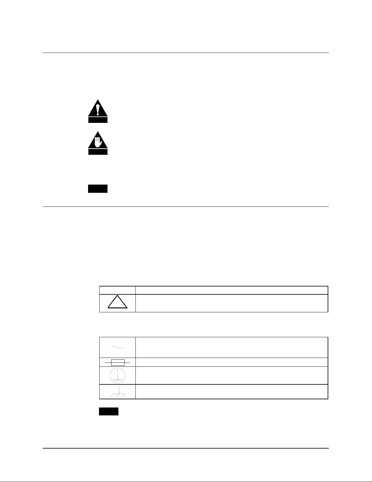
Caution and Warning
CAUTION indicates a hazardous situation that, if not avoided, may result in
minor or moderate injury. CAUTION may also be used to indicate other
CAUTION
unsafe practices or risks of property damage.
WARNING indicates a potentially hazardous situation that, if not avoided,
could result in death or serious injury.
WARN ING
Note
NOTE
This is the style for a note.
European EMC Directive
In order to meet the European Electro-Magnetic Compatibility (EMC) Directive
(EN55022, EN50082-1), properly shielded cables for DATA I/O are required. More
specifically, these cables must be double-shielded from end-to-end, ensuring a continuous
ground shield.
The following information is applicable for the European Low Voltage Directive
(EN60950):
<HAR> Type of power cord required for use in the European Community.
!
International Symbols:
CAUTION: Double-pole/Neutral Fusing
ACHTUNG: Zweipolige bzw. Neutralleiter-Sicherung
Alternating Current.
Fuse.
Safety Ground.
Chassis Ground.
NOTE
For additional symbols, refer to “Caution and Warning” listed earlier in
this preface.
ii
Page 7

D&I Revision 0
Preface MN/D-I.IOM
Reporting Comments or Suggestions Concerning this Manual
Comments and suggestions regarding the content and design of this manual will be
appreciated. To submit comments, please contact the EFData Customer Service
Department according to the following information.
Customer Service
Contact the EFData Customer Service Department for:
• Product support
• Information on returning a product
• Information on upgrading a product
• Product training
• Reporting comments or suggestions concerning manuals
An EFData Customer Service representative may be reached at:
EFData Corporation
Attention: Customer Service Department
2105 West 5th Place
Tempe, Arizona 85281 USA
(602) 968-0447
(602) 921-9012 FAX
or, E-Mail can be sent to the Customer Service Department at:
service@efdata.com
To return an EFData product (in-warranty and out-of-warranty) for repair or replacement:
1. Request a Return Material Authorization (RMA) number from the EFData
Customer Service Department.
Be prepared to supply the Customer Service representative with the model
number, serial number, and a description of the problem.
2. To ensure that the product is not damaged during shipping, pack the product in
its original shipping carton/packaging.
3. Ship the product back to EFData. (Shipping charges should be prepaid.)
For more information regarding the warranty policies, refer to the disclaimer page
located behind the title page.
iii
Page 8

D&I Revision 0
Preface MN/D-I.IOM
This page is intentionally left blank.
iv
Page 9

Table of Contents
PREFACE ........................................................................................................................ i
About this Manual ...................................................................................................................................................i
Organization .............................................................................................................................................................i
Revision Numbering Scheme...................................................................................................................................i
Conventions Used in this Manual ..........................................................................................................................ii
Caution and Warning............................................................................................................................................ii
Note ......................................................................................................................................................................ii
European EMC Directive .......................................................................................................................................ii
Reporting Comments or Suggestions Concerning this Manual.........................................................................iii
Customer Service ...................................................................................................................................................iii
CHAPTER 1. INTRODUCTION.................................................................................. 1–1
CHAPTER 2. CONNECTORS AND SWITCHES ....................................................... 2–1
2.1 Drop Data Input, Insert Data Output, and Ext. Ref CLK .......................................................................2–6
2.2 Drop Data Output (J2) ................................................................................................................................2–6
2.3 Insert Data Input (J3) ..................................................................................................................................2–7
2.4 Insert Data Output (J4) ............................................................................................................................... 2–7
2.5 Drop Data Input (J5) ...................................................................................................................................2–8
2.6 Drop Data Output (J6) ................................................................................................................................2–8
v
Page 10

D&I Revision 0
Preface MN/D-I.IOM
2.7 Insert Data Input (J7) ..................................................................................................................................2–8
2.8 Insert Data Output (J8) ............................................................................................................................... 2–9
2.9 External Reference Clock (J9) ....................................................................................................................2–9
2.10 ESC Channel (J10).....................................................................................................................................2–9
2.11 Faults (J11) ...............................................................................................................................................2–10
2.12 Data Interface (J12) .................................................................................................................................2–10
Figures
Figure 2-1. D&I Breakout Panel...................................................................................................................... 2–2
Figure 2-2. D&I Daughter Card Schematic .....................................................................................................2–3
Figure 2-3. D&I Breakout Panel Schematic ....................................................................................................2–4
Figure 2-3. D&I Breakout Panel Schematic (Cont’d) .....................................................................................2–5
Tables
Table 2-1. D&I Breakout Panel Connectors....................................................................................................2–2
Table 2-2. D&I Breakout Panel Switch Selections.......................................................................................... 2–3
vi
Page 11

Chapter 1. INTRODUCTION
The D&I (B-308-5) breakout panel provides standardized interfaces for the D&I
capabilities of the modem.
The balanced and unbalanced interfaces for drop DATA I/O and insert DATA I/O are
provided and are selectable with rear panel DIP switches.
This breakout panel is used in 1:1 or M:N switching configurations.
The D&I breakout panel supports the use of the D&I channel unit in the modem.
Refer to Chapter 2 for connector and switch information.
1–1
Page 12

D&I Revision 0
Introduction MN/D-I.IOM
This page is intentionally left blank.
1–2
Page 13

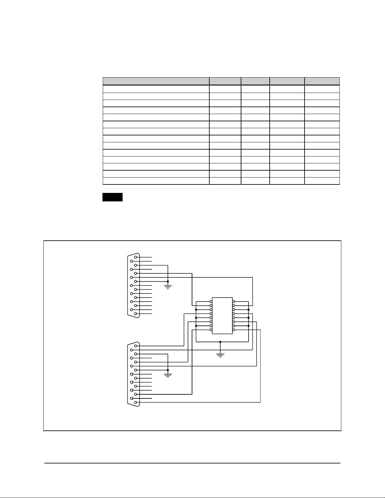
Chapter 2. CONNECTORS AND
SWITCHES
The locations of the connectors and D&I switches S1 through S5 are shown in
Figure 2-1.
Refer to Table 2-1 for D&I breakout panel connector information.
Refer to Table 2-2 for the D&I breakout panel switch selections.
The D&I PCB schematic is shown in Figure 2-2.
Refer to Figure 2-3 for the D&I breakout panel schematic.
2–1
Page 14

D&I Revision 0
Connectors ans Switches MN/D-I.IOM
DROP INPUT INSERT INPUT
J1
DROP OUTPUT
J2
INSERT OUTPUT
FRONT VIEW
J3
J4
DROP
IN OUT
J5 J6 J7
INSERT
IN
EXT REF
OUT
J8 J9
CLK
REAR VIEW
OPEN
1342
S3
CLOSED
J12 LOOP
NORM S4
S2
Figure 2-1. D&I Breakout Panel
Table 2-1. D&I Breakout Panel Connectors
J10
ESC
CHANNEL
OPEN
12345678 1
CLOSED
C
G
C
N
ONCN
O
NCN
PRI SEC
OPEN
345 78
S1
CLOSED
O
DCE
DTE
OMM
D
J11
FAULT S
S5
Ref Desig. Connector Type Name
J1 15-pin D Drop Data Input
J2 15-pin D Drop Data Output
J3 15-pin D Insert Data Input
J4 15-pin D Insert Data Output
J5 BNC Drop Data Input
J6 BNC Drop Data Output
J7 BNC Insert Data Input
J8 BNC Insert Data Output
J9 BNC Ext. Ref Clock
J10 25-pin D ESC Channel
J11 Terminal Block Faults
J12 50-pin D Data Interface
2–2
Page 15
D&I Revision 0
J
3
C
Connectors ans Switches MN/D-I.IOM
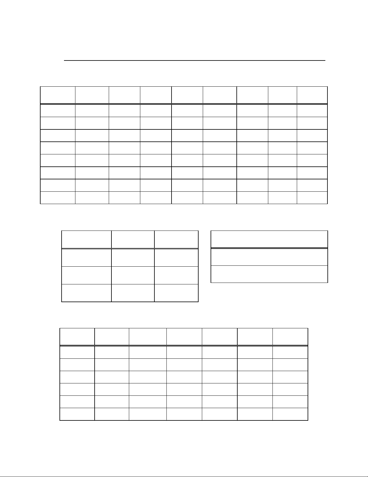
Table 2-2. D&I Breakout Panel Switch Selections
Signal Function Name Switch Switch # Position
Unbalanced Drop Data Input DDI S1 1, 2/3, 4 ON/OFF
Balanced Drop Data Input DDI S1 1, 2/3, 4 OFF/ON
Unbalanced Drop Data Output DDO S1 5, 6/7, 8 OFF/ON
Balanced Drop Data Output DDO S1 5, 6/7, 8 ON/OFF
Unbalanced Insert Data Input IDI S2 1, 2/3, 4 OFF/ON
Balanced Insert Data Input IDI S2 1, 2/3, 4 ON/OFF
Unbalanced Insert Data Output IDO S2 5, 6/7, 8 OFF/ON
Balanced Insert Data Output IDO S2 5, 6/7, 8 ON/OFF
Unbalanced Ext. Reference Clock EXC S3 1, 3/2, 4 OFF/ON
Balanced Ext. Reference Clock EXC S3 1, 3/2, 4 ON/OFF
Drop Output/Insert Input Loopback DDO/IDI S4 N/A UP
Normal S4 N/A DOWN
Drop Data Output DCE/DTE Select DDO S5 N/A UP
DCE/DTE S5 N/A DOWN
NOTE
S1 through S5 are ON in the down position (toward PCB).
1
9
2
10
3
11
4
12
5
13
6
14
7
15
8
DB15
DATA
INSERT
INPUT
J1
1
9
2
10
3
11
4
12
5
13
6
14
7
15
8
DB15
DROP DATA INPUT/
INSERT DATA OUTPUT /
EXT REF
LK
JP1
1 2
3 4
5 6
7 8
9 10
11 12
13 14
15 16
HEADER 8X2
Figure 2-2. D&I Daughter Card Schematic
2–3
Page 16

D&I Revision 0
Connectors ans Switches MN/D-I.IOM
J5
DROP DATA
INPUT
J6
DATA
DROP
OUTPUT
J2
1
9
2
10
3
11
4
12
5
13
6
14
7
15
8
DB15
DROP DATA
OUTPUT
J9
EXT
REF CLOCK
J7
INSERT DATA
INPUT
J8
INSERT
DATA
OUTPUT
J4
1
9
2
10
3
11
4
12
5
13
6
14
7
15
8
DB15
INSERT DATA
OUTPUT
T1
1
6
34
R1
470
52
2:1
XF8276
T2
1
6
34
R2
470
52
2:1
XF8276
S5
SW DPDT
DROP DATA OUTPUT
DCE/DTE SELECT
1
2
3
4
5
6
7
8
1
2
3
4
S1
SW DIP-8
S3
SW DIP-4
16
15
14
13
12
11
10
9
8
7
6
5
DDI-A
DDI-B
DDO-A
DDO-B
EXC-A
EXC-B
Cont.
next
page
A
IDI-A
IDI-B
S4
T5
1
6
34
R5
470
52
2:1
XF8276
T3
1
6
34
R3
470
52
2:1
XF8276
T4
1
6
34
R4
470
52
2:1
XF8276
IDO-A
IDO-B
HEADER
JP1
1 2
3 4
5 6
7 8
9 10
11 12
13 14
15 16
8X2
SW D PDT
DROP OUTPUT/
INSERT INPUT
LOOP
S2
1
2
3
4
5
6
7
8
SW DIP-8
DDO-A
DDO-B
IDI-A
16
IDI-B
15
14
13
12
IDO-A
IDO-B
11
10
9
Figure 2-3. D&I Breakout Panel Schematic
2–4
Page 17

D&I Revision 0
Connectors ans Switches MN/D-I.IOM
A
Cont.
from
previous
page
PRI_COM
PRI_NO
PRI_NC
SEC_COM
SEC_NO
SEC_NC
J11
1
2
3
4
5
6
7
8
8POSTERMBLK
TERTXDAT
TERRXDAT
RTS/C TS
DSR
J10
1
14
2
15
3
16
4
17
5
18
6
19
7
20
8
21
9
22
10
23
11
24
12
25
13
DB25
ESC
DDI-A
DDI-B
EXC-A
EXC-B
IDO- A
IDO-B
DDO-A
TERTXDAT
DDO-B
IDI-A
TERRXDAT
IDI-B
PRI_COM
PRI_NO
PRI_NC
SEC_COM
SEC_NO
SEC_NC
DSR
J12
1
P01
34
P34
18
P18
2
P02
35
P35
19
P19
3
P03
36
P36
20
P20
4
P04
37
P37
21
P21
5
P05
38
P38
22
P22
6
P06
39
P39
23
P23
7
P07
40
P40
24
P24
8
P08
41
P41
25
P25
9
P09
42
P42
26
P26
10
P10
43
P43
27
P27
11
P11
44
P44
28
P28
12
P12
45
P45
29
P29
13
P13
46
P46
30
P30
14
P14
47
P47
31
P31
15
P15
48
P48
32
P32
16
P16
49
P49
33
P33
17
P17
50
P50
DB50
Figure 2-3. D&I Breakout Panel Schematic (Cont’d)
2–5
Page 18

D&I Revision 0
Connectors ans Switches MN/D-I.IOM
2.1 Drop Data Input, Insert Data Output, and Ext. Ref CLK
This signal connection is a 15-pin female D connector (J1) located at the front of the
breakout panel. Screw locks are provided for mechanical security of the mating
connector.
Signal Function Name Pin #
Ground GND 2, 4
Insert Data Out IDO–A
IDO–B 3 11
External Clock EXC–A
EXC–B 7 8
Drop Data Input DDI–A
DDI–B
For J1 selections, use S1, S2, and S3, located at the rear of the breakout panel.
Signal Function Name Switch Switch # Position
Balanced Insert Data Output IDO S2 5, 6/7, 8 ON/OFF
Balanced Drop Data Input DDI S1 1, 2/3, 4 ON/OFF
Balanced External Clock EXC S3 1, 3/2, 4 ON/OFF
1
9
2.2 Drop Data Output (J2)
The balanced drop data output connection is a 15-pin female D connector located at the
front of the breakout panel. Screw locks are provided for mechanical security of the
mating connector.
Signal Function Name Pin #
Ground GND 2, 4
Drop Data Output DDO–A
Drop Data Output DDO–A
For J2 selections, use S1 and S5 located at the rear of the panel.
Signal Function Name Switch Switch # Position
Balanced Drop Data Output
(DCE/DTE Select)
Unbalanced Drop Data Output DDO S1 5, 6/7, 8 OFF/ON
Balanced Drop Data Output DDO S1 5, 6/7, 8 ON/OFF
NOTE
S1 is ON in the down position (toward PCB).
DDO–B 1 9
DDO–B 3 11
DDO S5 N/A UP
2–6
Page 19

D&I Revision 0
Connectors ans Switches MN/D-I.IOM
2.3 Insert Data Input (J3)
The balanced insert data input connection is a 15-pin female D connector located at the
front of the breakout panel. Screw locks are provided for mechanical security of the
mating connector.
Signal Function Name Pin #
Ground GND 2, 4
Insert Data Input IDI–A
IDI–B 3 11
For J3 selections, use S2 located at the rear of the panel.
Signal Function Name Switch Switch # Position
Unbalanced Insert Data Input IDI S2 1, 2/3, 4 OFF/ON
Balanced Insert Data Input IDI S2 1, 2/3, 4 ON/OFF
NOTE
S2 is ON in the down position (toward PCB).
2.4 Insert Data Output (J4)
The balanced insert data output connection is a 15-pin female D connector located at the
front of the breakout panel. Screw locks are provided for mechanical security of the
mating connector.
Signal Function Name Pin #
Ground GND 2, 4
Insert Data Output IDO–A
For J4 selections, use S2 located at the rear of the panel.
Signal Function Name Switch Switch # Position
Unbalanced Insert Data Output IDO S2 5, 6/7, 8 OFF/ON
Balanced Insert Data Output IDO S2 5, 6/7, 8 ON/OFF
NOTE
S2 is ON in the down position (toward PCB).
IDO–B
3
11
2–7
Page 20

D&I Revision 0
Connectors ans Switches MN/D-I.IOM
2.5 Drop Data Input (J5)
The unbalanced and balanced drop data input connection is a BNC connector located at
the front of the breakout panel. For J5 selections, use S1 located at the rear of the panel.
Signal Function Name Switch Switch # Position
Unbalanced Drop Data Input DDI S1 1, 2/3, 4 ON/OFF
Balanced Drop Data Input DDI S1 1, 2/3, 4 OFF/ON
NOTE
S1 is ON in the down position (toward PCB).
2.6 Drop Data Output (J6)
The unbalanced and balanced drop data output connection is a BNC connector located at
the front of the breakout panel. For J6 selections, use S1 located at the rear of the panel.
Signal Function Name Switch Switch # Position
Unbalanced Drop Data Output DDO S1 5, 6/7, 8 OFF/ON
Balanced Drop Data Output DDO S1 5, 6/7, 8 ON/OFF
NOTE
S1 is ON in the down position (toward PCB).
2.7 Insert Data Input (J7)
The unbalanced and balanced insert data input connection is a BNC connector located at
the front of the breakout panel. For J7 selections, use S2 located at the rear of the panel.
Signal Function Name Switch Switch # Position
Unbalanced Insert Data Input IDI S2 1, 2/3, 4 OFF/ON
Balanced Insert Data Input IDI S2 1, 2/3, 4 ON/OFF
NOTE
S1 is ON in the down position (toward PCB).
2–8
Page 21

D&I Revision 0
Connectors ans Switches MN/D-I.IOM
2.8 Insert Data Output (J8)
The unbalanced and balanced insert data output connection is a BNC connector located at
the front of the breakout panel. For J8 selections, use S2 located at the rear of the panel.
Signal Function Name Switch Switch # Position
Unbalanced Insert Data Output IDO S2 5, 6/7, 8 OFF/ON
Balanced Insert Data Output IDO S2 5, 6/7, 8 ON/OFF
NOTE
S2 is ON in the down position (toward PCB).
2.9 External Reference Clock (J9)
The unbalanced and balanced external reference clock input is a BNC connector located
at the front of the breakout panel. For J9 selections, use S3, located at the rear of the
panel.
Signal Function Name Switch Switch # Position
Unbalanced External
Reference Clock
Balanced External
Reference Clock
NOTE
S3 is ON in the down position (toward PCB).
EXC S3 1, 3/2, 4 OFF/ON
EXC S3 1, 3/2, 4 ON/OFF
2.10 ESC Channel (J10)
The ESC Channel interface is a 25-pin female D connector located at the front of the
breakout panel. Screw locks are provided for mechanical security of the mating
connector.
Signal Function Name Pin #
Ground GND 1, 7
Terrestrial Tx Data
Terrestrial Rx Data
Request To Send RTS 4
Clear To Send CTS 5
Data Set Ready DSR 6
NOTE
RTS and CTS are looped together on the connector.
TER–TXDAT
TER–RXDAT
2–9
2
3
Page 22

D&I Revision 0
Connectors ans Switches MN/D-I.IOM
2.11 Faults (J11)
The Faults connection is an 8-position terminal block located at the front of the breakout
panel.
Signal Function Name Pin #
Ground GND 1, 5
Primary Common
Primary Norm/Open
Primary Norm/Closed
Secondary Common
Secondary Normally Open
Secondary Normally Closed
PRI–COM
PRI–NO
PRI–NC
SEC–COM
SEC–NO
SEC–NC
2
3
4
6
7
8
2.12 Data Interface (J12)
The data interface connection is a 50-pin female D connector located at the rear of the
breakout panel. Screw locks are provided for mechanical security of the mating
connector.
Signal Function Name Pin #
Ground GND 1, 2
Drop Data Input DDI–A
DDI–B
External Clock EXC–A
EXC–B
Insert Data Output IDO–A
IDO–B
Drop Data Output DDO–A
DDO–B
Terrestrial Tx Data
Terrestrial Rx Data
Insert Data Input IDI–A
Primary Common
Primary Normally Open
Primary Normally Closed
Secondary Common
Secondary Normally Open
Secondary Normally Closed
Data Set Ready DSR 48
Terrestrial ESC DSR TER–ESC–DSR 41
TER–TXDAT
TER–RXDAT
IDI–B
PRI–COM
PRI–NO
PRI–NC
SEC–COM
SEC–NO
SEC–NC
34
18
35
19
36
20
37
38
5
7
39
40
10
43
27
11
44
28
2–10
Page 23
METRIC CONVERSIONS
Units of Length
Unit
1 centimeter — 0.3937 0.03281 0.01094
1 inch 2.540 — 0.08333 0.2778
1 foot 30.480 12.0 — 0.3333
1 yard 91.44 36.0 3.0 —
Centimeter
Inch
Foot
Yard
Mile
6.214 x 10
1.578 x 10
1.893 x 10
5.679 x 10
Meter
-6
-5
-4
-4
0.01 — —
0.254 — 25.4
0.3048 — —
0.9144 — —
Kilometer Millimeter
1 meter 100.0 39.37 3.281 1.094
1 mile
1 mm — 0.03937 — — — — — —
1 kilometer — — — — 0.621 — — —
1.609 x 10
5
6.336 x 10⁴ 5.280 x 10³ 1.760 x 10³
6.214 x 10
-4
—
— — —
1.609 x 10³
1.609 —
Temperature Conversions
Unit
32° Fahrenheit
212° Fahrenheit
-459.6° Fahrenheit
° Fahrenheit
—
—
—
° Centigrade
0
(water freezes)
100
(water boils)
273.1
(absolute 0)
Formulas
C = (F - 32) * 0.555
F = (C * 1.8) + 32
Units of Weight
Unit
1 gram — 0.03527 0.03215 0.002205 0.002679 0.001
Gram
Ounce
Avoirdupois
Ounce
Troy
Pound
Avoir.
Pound
Troy
Kilogram
1 oz. avoir. 28.35 — 0.9115 0.0625 0.07595 0.02835
1 oz. troy 31.10 1.097 — 0.06857 0.08333 0.03110
1 lb. avoir. 453.6 16.0 14.58 — 1.215 0.4536
1 lb. Troy 373.2 13.17 12.0 0.8229 — 0.3732
1 kilogram
1.0 x 10
3
35.27 32.15 2.205 2.679 —
Page 24

2114 WEST 7TH STREET TEMPE ARIZONA 85281 USA
480 • 333 • 2200 PHONE
480 • 333 • 2161
FAX
 Loading...