

Page 1

DD2401 VME
L-Band Demod Card
Installation and Operation Manual
MN-VME2401
Revision B
Comtech EF Data • 2114 W 7th St. • Tempe, AZ 85281 • (480) 333-2200 • Fax: (480) 333-2540 • www.comtechefdata.com
Page 2

Page 3

DD2401 VME L-Band Demodulator Card Installation & Operational Manual Warranty Policy
WP
Warranty Policy
Comtech EF Data products are warranted against defects in material and workmanship for a period of two
years from the date of shipment. During the warranty period, Comtech EF Data will, at its option, repair or
replace products that prove to be defective.
For equipment under warranty, the owner is responsible for freight to Comtech EF Data and all related
customs, taxes, tariffs, insurance, etc. Comtech EF Data is responsible for the freight charges only for return
of the equipment from the factory to the owner. Comtech EF Data will return the equipment by the same
method (i.e., Air, Express, Surface) as the equipment was sent to Comtech EF Data.
All equipment returned for warranty repair must have a valid RMA number issued prior to return and be
marked clearly on the return packaging. Comtech EF Data strongly recommends all equipment be returned
in its original packaging.
Comtech EF Data Corporation’s obligations under this warranty are limited to repair or replacement of failed
parts, and the return shipment to the buyer of the repaired or replaced parts.
Limitations of Warranty
The warranty does not apply to any part of a product that has been installed, altered, repaired, or misused in
any way that, in the opinion of Comtech EF Data Corporation, would affect the reliability or detracts from the
performance of any part of the product, or is damaged as the result of use in a way or with equipment that
had not been previously approved by Comtech EF Data Corporation.
The warranty does not apply to any product or parts thereof where the serial number or the serial number of
any of its parts has been altered, defaced, or removed.
The warranty does not cover damage or loss incurred in transportation of the product.
The warranty does not cover replacement or repair necessitated by loss or damage from any cause beyond
the control of Comtech EF Data Corporation.
The warranty does not cover any labor involved in the removal and or reinstallation of warranted equipment
or parts on site, or any labor required to diagnose the necessity for repair or replacement.
The warranty excludes any responsibility by Comtech EF Data Corporation for incidental or consequential
damages arising from the use of the equipment or products, or for any inability to use them either separate
from or in combination with any other equipment or products.
A fixed charge established for each product will be imposed for all equipment returned for warranty repair
where Comtech EF Data Corporation cannot identify the cause of the reported failure.
Exclusive Remedies
Comtech EF Data Corporation’s warranty, as stated is in lieu of all other warranties, expressed, implied, or
statutory, including those of merchantability and fitness for a particular purpose. The buyer shall pass on to
any purchaser, lessee, or other user of Comtech EF Data Corporation’s products, the aforementioned
warranty, and shall indemnify and hold harmless Comtech EF Data Corporation from any claims or liability of
such purchaser, lessee, or user based upon allegations that the buyer, its agents, or employees have made
additional warranties or representations as to product preference or use.
The remedies provided herein are the buyer’s sole and exclusive remedies. Comtech EF Data shall not be
liable for any direct, indirect, special, incidental, or consequential damages, whether based on contract, tort,
or any other legal theory.
MN-VME2401 – Rev. B iii
Page 4

Warranty Policy DD2401 VME L-Band Demodulator Card Installation & Operational Manual
Warranty Repair Return Procedure
Before a warranty repair can be accomplished, a Repair Authorization must be received. It is at this time
that Comtech EF Data will authorize the product or part to be returned to the Comtech EF Data facility or if
field repair will be accomplished. The Repair Authorization may be requested in writing or by calling:
Comtech EF Data Corporation
2114 W 7
th
Street.
Tempe, Arizona 85281 (USA)
ATTN: Customer Support
Phone: (480) 333-2200
Fax: (480) 333-2540
Any product returned to Comtech EF Data for examination must be sent prepaid via the means of
transportation indicated as acceptable to Comtech EF Data. Return Authorization Number must be clearly
marked on the shipping label. Returned products or parts should be carefully packaged in the original
container, if possible, and unless otherwise indicated, shipped to the above address.
Non-Warranty Repair
When a product is returned for any reason, Customer and its shipping agency shall be responsible for all
damage resulting from improper packing and handling, and for loss in transit, not withstanding any defect or
nonconformity in the product. By returning a product, the owner grants Comtech EF Data permission to
open and disassemble the product as required for evaluation. In all cases, Comtech EF Data has sole
responsibility for determining the cause and nature of failure, and Comtech EF Data’s determination with
regard thereto shall be final.
iv MN-VME2401 – Rev. B
Page 5
DD2401 VME L-Band Demodulaotr Card Installation & Operational Manual Preface
P
Preface
This manual provides installation and operation information for the Radyne DD2401 VME L-Band
Demodulator Card. This is a technical document intended for use by engineers, technicians, and
operators responsible for the operation and maintenance of the DD2401 VME Demodulator Card.
Cautions and Warnings
A caution icon indicates a hazardous situation that if not avoided, may result in minor or moderate
injury. Caution may also be used to indicate other unsafe practices or risks of property damage.
A warning icon indicates a potentially hazardous situation that if not avoided, could result in death
or serious injury.
A note icon identifies information for the proper operation of your equipment, including helpful
hints, shortcuts, or important reminders.
Trademarks
Product names mentioned in this manual may be trademarks or registered trademarks of their
respective companies and are hereb y acknowledged.
MN-VME2401 – Rev. B v
Page 6
Preface DD2401 VME L-Band Demodulaotr Card Installation & Operational Manual
Revision
Level
Copyright
2009, Comtech EF Data This manual is proprietary to Comtech EF Data and is intended for the
exclusive use of Comtech EF Data’s customers. No part of this document may in whole or in
part, be copied, reproduced, distributed, translated or reduced to any electronic or magnetic
storage medium without the express written consent of a duly authorized officer of Comtech EF
Data
Disclaimer
This manual has been thoroughly reviewed for accuracy. All statements, technical information,
and recommendations contained herein and in any guides or related documents are believed
reliable, but the accuracy and completeness thereof are not guaranteed or warranted, and they
are not intended to be, nor should they be understood t o be, represe nt at ions or war ranti es
concerning the products described. Comtech EF Data assumes no responsibility for use of any
circuitry other than the circuitry employed in Comtech EF Data systems and equipment.
Furthermore, since Comtech EF Data is constantly improving its products, reserves the right to
make changes in the specifications of products, or in this manual at any time without notice and
without obligation to notify any person of such changes .
Record of Revisions
Date Reason for Change
1.0 04-01-98 New Release.
A 12-16-08 Updated Terrestrial Interfaces.
B 2-23-09 Clarified use of 8PSK. Technical specifications made to match other product
lines
Comments or Suggestions Concerning this Manual
Comments or suggestions regarding the content and design of this manual are appreciated.
To submit comments, please contact the Comtech EF Data Corporation Customer Service
Department.
vi MN-VME2401 – Rev. B
Page 7

DD2401 VME L-Band Demodulaor Card Installation & Operational Manual Table of Contents
ToC
Table of Contents
Section 1 - Introduction ............................................................................................. 1-1
1.0 Description ______________________________________________________ 1-1
1.1 DD2401 VME Demodulator Card Available Options _______________________ 1-2
1.1.1 Reed-Solomon Codec (Optional) ____________________________________ 1-2
1.1.2 Turbo Codec (Optional)_ __________________________________________ 1-2
1.1.3 8PSK (Optional) ________________________________________________ 1-2
Section 2 - Installation ............................................................................................... 2-1
2.0 Installation Requirements ___________________________________________ 2-1
2.1 Unpacking _______________________________________________________ 2-1
2.2 Removal and Assembly ____________________________________________ 2-1
2.3 Mounting Considerations ___________________________________________ 2-1
2.4 Demodulator Checkout _____________________________________________ 2-1
2.4.1 Initial Power-Up _________________________________________________ 2-1
2.4.2 Factory Terminal Setup (Refer to Section 4.4) __________________________ 2-2
2.4.3 Remote Protocol Factory Default Setup _______________________________ 2-2
2.5 Storage ________________________________________________________ 2-2
Section 3 - Theory of Operation ................................................................................ 3-1
3.0 Theory of Operation _______________________________________________ 3-1
3.1 Applications ______________________________________________________ 3-2
3.1.1 SCPC Point-to-Point Links _________________________________________ 3-2
3.1.2 SCPC Point to Multi–Point Links in a Broadcast Application _______________ 3-2
3.1.3 DAMA (Demand Assigned Multiple Access) ___________________________ 3-3
3.1.4 TDMA (Time Division Multiple Access) Remote Site Application ____________ 3-3
3.2 VME Demodulator Card Reed-Solomon ________________________________ 3-3
3.2.1 Reed-Solomon Codec ____________________________________________ 3-3
3.2 Clocking Options __________________________________________________ 3-4
3.2.1 RX Buffer Clock Options __________________________________________ 3-4
MN-VME2401 – Rev. B vii
Page 8

Table of Contents DD2401 VME L-Band Demodulator Card Installation & Operational Manual
3.2.1.1 RX SAT Clock _________________________________________________ 3-5
3.2.1.2 SCT: Serial Clock Transmit _______________________________________ 3-5
3.2.2 EXT REF: External Reference, J2 ___________________________________ 3-5
3.2.3 Reed-Solomon Operation in the DD2401 VME Demodulator Card __________ 3-5
3.2.4 Reed-Solomon Code Rate _________________________________________ 3-5
3.2.5 Interleaving_____________________________________________________ 3-6
Section 4 - User Interfaces ........................................................................................ 4-1
4.0 User Interfaces ___________________________________________________ 4-1
4.1 Remote Port Control (J3) ___________________________________________ 4-1
4.2 Terminal Mode Control (J1) _________________________________________ 4-1
4.3 Terminal Port User Interface _________________________________________ 4-2
4.3.1 Connecting the Terminal __________________________________________ 4-2
4.3.2 Terminal Screens ________________________________________________ 4-3
4.4 Remote Port User Interface _________________________________________ 4-6
4.4.1 Protocol Structure _______________________________________________ 4-6
4.4.2 Protocol Wrapper ________________________________________________ 4-6
4.4.3 Frame Description and Bus Handshaking _____________________________ 4-8
4.4.4 Global Response Operational Codes _________________________________ 4-8
4.4.5 Collision Avoidance _____________________________________________ 4-10
4.4.6 Software Compatibility ___________________________________________ 4-11
4.4.7 Flow Control and Task Processing _________________________________ 4-11
4.4.8 RLLP Summary ________________________________________________ 4-12
4.4.9 DD2401/DD2401L Opcode Command Set ___________________________ 4-13
4.4.11 Module Command Set __________________________________________ 4-14
4.4.12 Detailed Command Descriptions __________________________________ 4-14
4.4.12.1 DMD2401 Demodulator _______________________________________ 4-14
4.4.12.2 Module Queries & Commands __________________________________ 4-35
4.4.12.3 Default Values Demodulator ____________________________________ 4-39
Section 5 - Rear Panel Interfaces .............................................................................. 5-1
5.0 DD2401 VME Demodulator Card Connections ___________________________ 5-1
5.1 Power ________________________________________________________ 5-2
5.1.1 Diagnostic LED's ________________________________________________ 5-2
5.2 Terrestrial Data I/F ________________________________________________ 5-3
viii MN-VME2401 – Rev. B
Page 9

DD2401 VME L-Band Demodulaor Card Installation & Operational Manual Table of Contents
5.3 EXT REF ________________________________________________________ 5-4
5.4 SERIAL CONTROL I/F _____________________________________________ 5-4
5.5 RX IN ________________________________________________________ 5-4
5.5.1 L-Band ________________________________________________________ 5-4
5.6 Remote Port _____________________________________________________ 5-4
5.7 Remote Addresses ________________________________________________ 5-5
Section 6 - Maintenance and Troubleshooting ........................................................ 6-1
6.0 Periodic Maintenance ______________________________________________ 6-1
Section 7 - Technical Specifications ......................................................................... 7-1
7.0 Introduction ______________________________________________________ 7-1
7.1 Receive Data Rates _______________________________________________ 7-1
7.2 Demodulator Specifications _________________________________________ 7-1
7.3 Options ________________________________________________________ 7-1
7.4 Environmental ____________________________________________________ 7-1
7.5 Physical ________________________________________________________ 7-2
7.6 BER Charts ______________________________________________________ 7-3
7.7 AGC Curve _____________________________________________________ 7-12
Glossary ..................................................................................................................... G-1
MN-VME2401 – Rev. B ix
Page 10

Table of Contents DD2401 VME L-Band Demodulator Card Installation & Operational Manual
x MN-VME2401 – Rev. B
Page 11
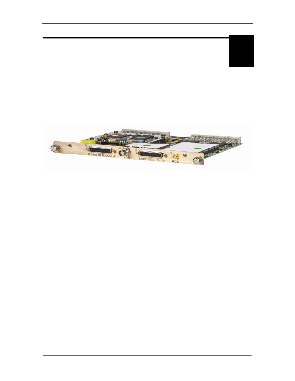
DD2401 VME L-Band Demodulator Card Installation & Operational Manual Introduction
1
Introduction
1.0 Description
The Radyne DD2401 VME L-Band Demodulator is intended for use as apart of the receiving
ground equipment in a satellite communication system. The card based unit is designed to
receive a single carrier up to 5 MBits/s throughput on the RS422 synchronous interfaces. The
DD2401 VME card is compatibility with all Radyne's DMD products including the DMD20, DMD50
and OM20.
Figure 1-1. DD2401 VME L-Band Demodulator Card
The DD2401 VME Demodulator Card is designed to perform at one end of the satellite Single
Channel Per Carrier (SCPC) Link receiving the carrier. The VME can be used in a Mesh or Star
Topology Network. The Demodulator supports BPSK, QPSK, OQPSK or 8PSK demodulation.
The demodulator can be accessed via a single RS485 serial link system for complete remote
monitor and control (M&C) capability and offers the terminal control via an RS232 connection.
Selection of any data rate is provided over the following ranges:
BPSK: 9.6 Kbps to 1200 Kbps
QPSK: 9.6 Kbps to 4.375 Mbps
OQPSK: 9.6 Kbps to 4.375 Mbps
8PSK: 64.0 Kbps to 5.0 Mbps
The VME Demodulator Card can track and acquire a carrier over a programmable range of ± 1
kHz to ± 42 kHz. Acquisition times of less than three seconds are typical at data rates greater
than 64 Kbps over a range of ± 25 kHz.
To facilitate link testing, the VME Demodulator Card incorporates a built-in ‘2047’ tes t patter n with
BER measurement capability.
MN-VME2401 – Rev. B 1-2
Page 12

Introduction DD2401 VME L-Band Demodulator Card Installation & Operational Manual
1.1 DD2401 VME L-Band Demodulator Card Available Options
Various options are available for the DD2401 VME L-Band Demodulator Card:
1.1.1 Reed-Solomon Codec (Optional)
The VME Demodulator Card is equipped w ith an Intelsat Reed-Solomon Outer Codec with an
interleaver as an optional enhancement for applications requiring Bit Error Rates (BER) of 10
The encoder and decoder are completely independent and meet the IESS-308/309 Specification.
-10
.
1.1.2 Turbo Codec (Optional)
The VME Card is equipped with Turbo Product Code (TPC) Codec. TPC Codes include 0.495
and 0.793, 21/44, 1/2, 3/4 and 7/8 Rate.
1.1.3 8PSK (Optional)
The VME Card offers in addition to the standard B/O/QPSK waveforms an 8PSK optional high
order waveform capable of either Trellis 2/3 or any TPC 0.495, TPC0.793, TPC 3/4 and TPC 7/8
when purchased wit the Turbo option.
1-2 MN-VME2401 – Rev. B
Page 13

DD2401 VME L-Band Demodulator Card Installation & Operational Manual Introduction
MN-VME2401 – Rev. B 1-2
Page 14

Page 15

DD2401 VME L-Band Demodulator Card Installation & Operational Manual Installation
2
Installation
This section provides unpacking and installation instructions, and a description of external
connections.
2.0 Installation Requirements
The VME2401 demodulator card is designed to be installed within any standard VME-compliant
cabinet.
2.1 Unpacking
The VME Demodulator Card was carefully packaged to avoid damage and should arrive
complete with the following items for proper installation:
1. VME L-Band Demodulator Card
2. Installation and Operation Manual
2.2 Removal and Assembly
If using a knife or cutting blade to open the carton, exercise caution to insure that the blade does
not extend into the carton, but only cuts the tape holding the carton closed. Carefully unpack the
unit and ensure that all of the above items are in the carton.
2.3 Mounting Considerations
When mounted in an equipment cabinet, ad equ ate ve nti lat ion m ust be prov ided. T he am bient
temperature in the cabinet should preferably be between 10° a nd 35° C, and held constant for
best equipment operation. The air available to the cabinet should be clean and relatively dry. The
unit should not be placed immediately above a high heat or EMF generator to ensure the output
signal integrity and proper receive operation.
2.4 Demodulator Checkout
The following descript ions assume that the VME Demodulator Card is installed in a suitable
chassis.
2.4.1 Initial Power-Up
The VME Demodulator Card is shipped from the factory with preset factory defaults. upon initial
power-up, a user check should be performed to verify the shipped demodulator configuration.
The following are standard VME Demodulator Card Factory Configuration Settings:
Data Rate: 2,048 Kbps
Forward Error Correction (FEC): 1/2 Rate Viterbi
Frequency: 950 MHz (L-Band)
Interface: RS422
MN-VME2401 – Rev. B 2-1
Page 16
Installation DD2401 VME L-Band Demodulator Card Installation & Operational Manual
Position
Position
Position
Position
on
The connector definitions and pinout tables are shown in secti on 5.0. Any connection interfacing
to the modem must be the appropriate mating connector.
Shielded cables with the shield terminated to conductive backshells are required in
order to meet EMC directives. Cables with insulation flammability ratin g s of 94 VO or
better are required in order to meet Low Vo ltage Directives.
2.4.2 Factory Terminal Setup (Refer to Section 4.4)
The factory terminal setup is as follows:
Emulation Type: VT-100 (can be changed)
Baud Rate: 19200
Data Bits 8
Parity: No Parity (Fixed)
Stop Bits: 1
2.4.3 Remote Protocol Factory Default Setup
Demodulator will be configured with default settings when they are shipped from factory. Refer to
Section 5-6 to Defaults setting can be modified may be the default settings for the RS485
Communication port are:
Table 2-1. S1 DIP Switches
Demodulator
Demodullator
1
2
off off off 33
3
4
Address in
Decimal
2.5 Storage
It is recommended that the unit be stored in its original sealed packaging. The unit should be
stored in a dry location where the temperature is stable, away from direct contact with rain, snow,
wind, sun or anything that may cause damage.
2-2 MN-VME2401 – Rev. B
Page 17

DD2401 VME L-Band Demodulator Card Installation & Operational Manual Installation
MN-VME2401 – Rev. B 2-3
Page 18

Page 19
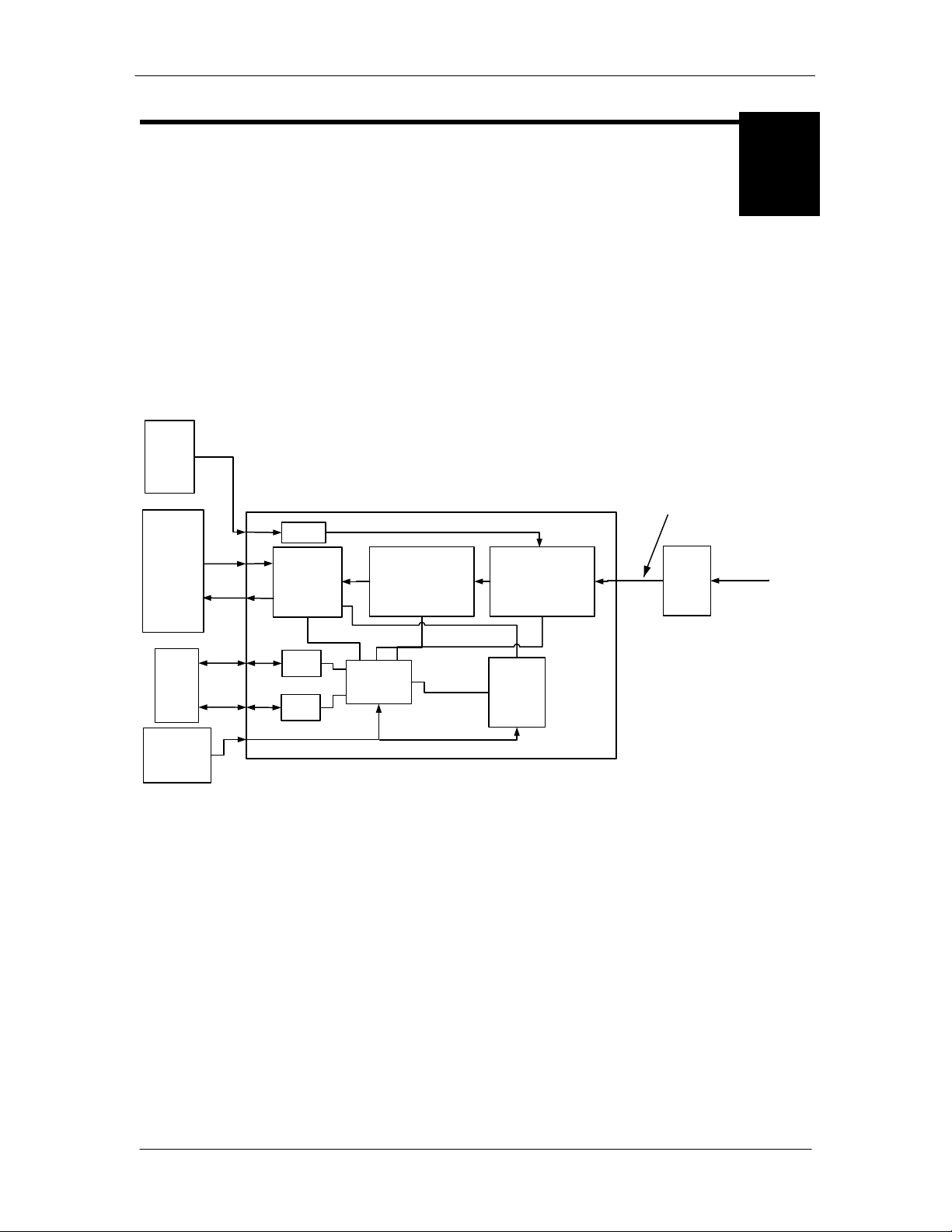
DD2401 VME L-Band Demodulator Card Installation & Operational Manual Theory of Operation
3
Rx
Baseband
Processing
Terminal
Remote
Port
M&C
Remote
Serial
Interfaces
Demodulator
RX RF
Equipment
Power Supply
+5 VDC
+12VDC
-12VDC
Terrestrial Data
Interface
Customer
Data
Terrestrial I/O
Modulator
Interconnect
Antenna
Demodulator Card
External
Referance
DD2401 VME Block Diagram
IF Input 950-1750 MHz
-25 to -55 dBm
Reference
Theory of Operation
3.0 Theory of Operation
The VME L-Band Demodulator Card is capable of receiving four L-Band signals between 9501750 MHz. The IF signals are then converted into data. The data is digitally filtered, passed
through the Viterbi FEC, differentially decoded and descrambled before it is sent to the RS422
terrestrial interface. The RS422 data from each demodulator can be retrieving from the rear
panels of each demodulator.
Figure 3-1. DD2401 VME Demodulator Block Diagram
MN-VME2401 – Rev. B 3-1
Page 20
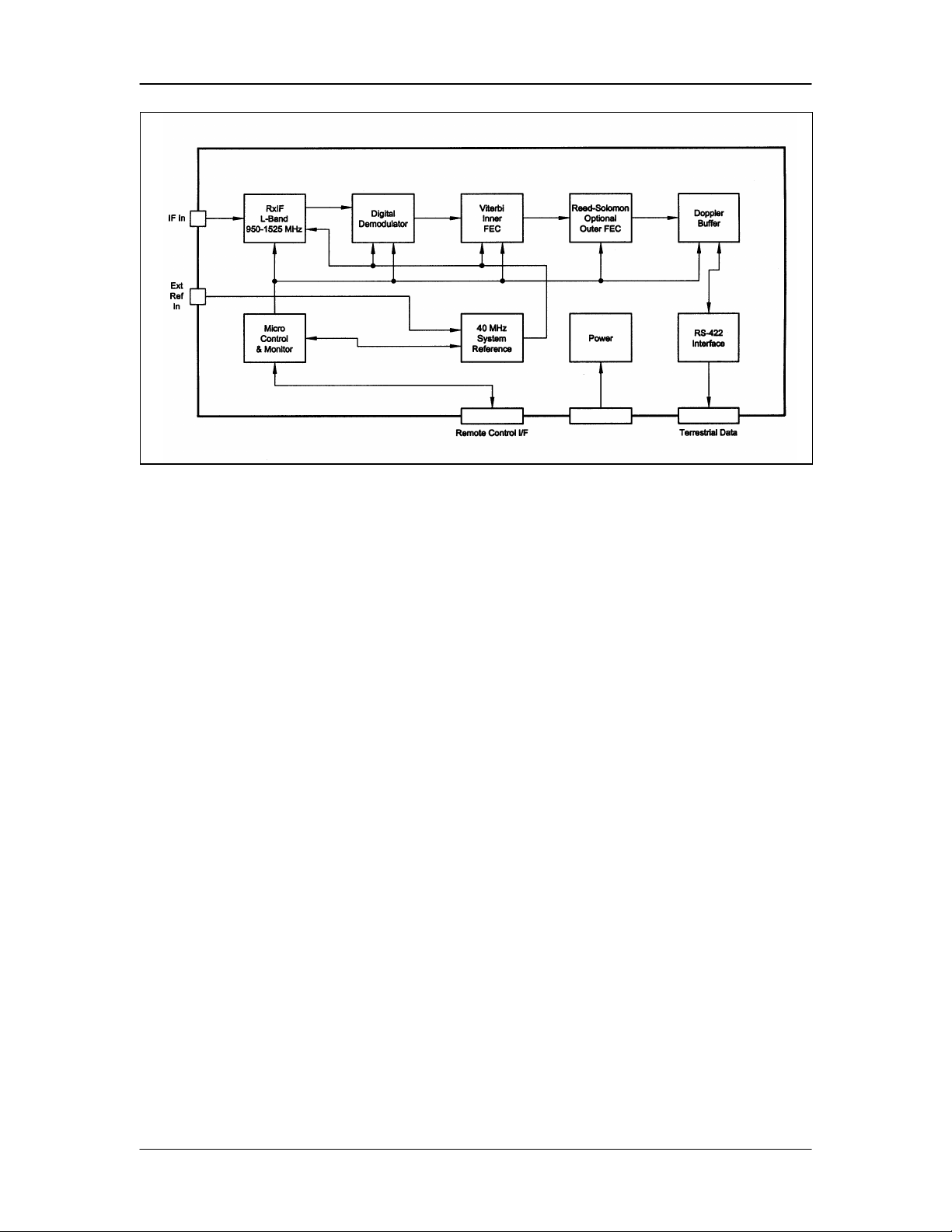
Theory of Operation DD2401 VME L-Band Demodulator Card Installation & Operational Manual
Figure 3-2. DD2401 VME L-Band Demodulator Block Diagram
3.1 Applications
Following are just a fe w representative forms of satellite c ommunications links and networks in
which the DD2401 VME Demodulator Card may be used.
3.1.1 SCPC Point-to-Point Links
The most straightforward application for a Satellite Demodulator is to serve as the Data
Communications Equipment (DCE) for a Point-to-Point Data Link. When used in this mode, two
demodulators located at two different sites are tuned to complementary transmit and receive
frequencies. Each direction of the communications link may have the same or entirely different
transmission parameters. In this application, it is typical that the link is established and
maintained on a continuous basis, although a special “on demand” case is described later.
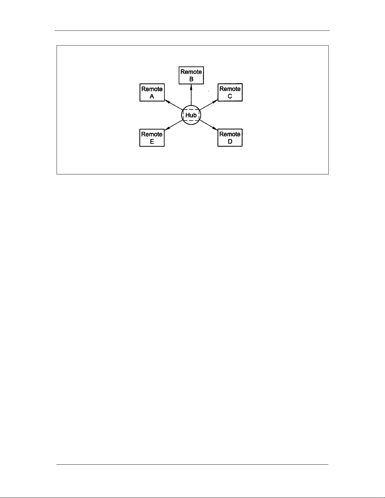
3.1.2 SCP C Point to Multi–Point Links in a Broadcast Application
A broadcast application might involve the necessity of sending continuous or intermittent data
from one source and “broadcasting” the information to many remote locations. For instance,
constant pricing information and updates may be sent by a central location to many store
locations. There may be minor return information from the remotes acknowledging receipt.
Another broadcast application could be transmitting background music from a central location to
many store sites. In this case, there would be no return path.
The topology of the network in both of these broadcast examples would typically be called a
“Star” Network. As shown in Figure 3-3, the shape of the configuration is drawn with the central
“Hub” as the center of the star and the remotes as points of the star. In both cases the transmit
frequency and other parameters are shared by the receiver of all the remotes.
3-2 MN-VME2401 – Rev. B
Page 21
DD2401 VME L-Band Demodulator Card Installation & Operational Manual Theory of Operation
Figure 3-3. Star Network Configuration
3.1.3 DAMA (Demand Assigned Multiple Access)
If a telephone network is to be simulated with a virtual switch between demodulators carrying
digitized voice information. A central computer might be used to assign a pair of frequencies for
any conversation and send this connection information to the proper sites to set up the
connection. In this application, a new network called a “Mesh” Network is required. Any of the
voice demodulators at any site can be programmed to link with any other demodulator. The
resulting link diagram looks like a mesh of interconnects.
Since the frequencies can be assigned on demand, the network is called “Demand Assigned,
Multiple Access,” or DAMA.
3.1.4 TDMA (Time Division Multiple Access) Remote Site Application
In a TDMA Network, the central Hub continually transmits a stream of outbound data containing
information for multiple remote sites, while the remote sites transmit back to the Hub on a timed
basis. Each of these remotes is said to “burst” its information back on a specific frequency. This
may be the same inbound frequency for all sites.
Each of the remotes is responsible for accessing its own information from the outbound data
stream by reading the address assigned to specific parts of the data. The TDMA Network usually
looks like the Star network described above.
The DD2401 VME Demodulator Card is specifically designed to be usable as the remote site
Demodulator of a TDMA network when coupled with a proper “Burst” Demodulator at the hub site.
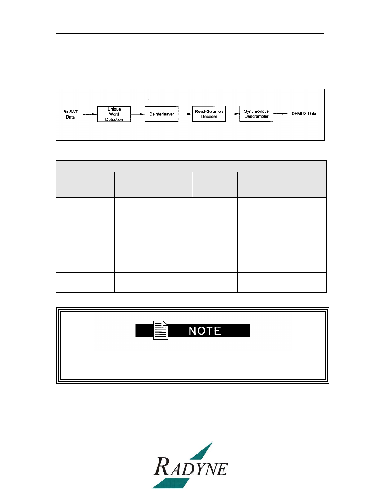
3.2 VME Demodulator Card Reed-Solomon
3.2.1 Reed-Solomon Codec
Utilizing a Reed-Solomon (RS) Outer Codec concatenated with a convolutional inner codec is an
effective way to produce very low error rates even for poor signal-to-noise ratios while requiring
only a small increase in transmission bandwidth. Typically, concatenating an RS Codec requires
an increase in transmission bandwidth of only nine to twelve percent while producing a greater
than 2 dB improvement in Eb/No. RS is a block codec where K data bytes are fed into the
MN-VME2401 – Rev. B 3-3
Page 22
Theory of Operation DD2401 VME L-Band Demodulator Card Installation & Operational Manual
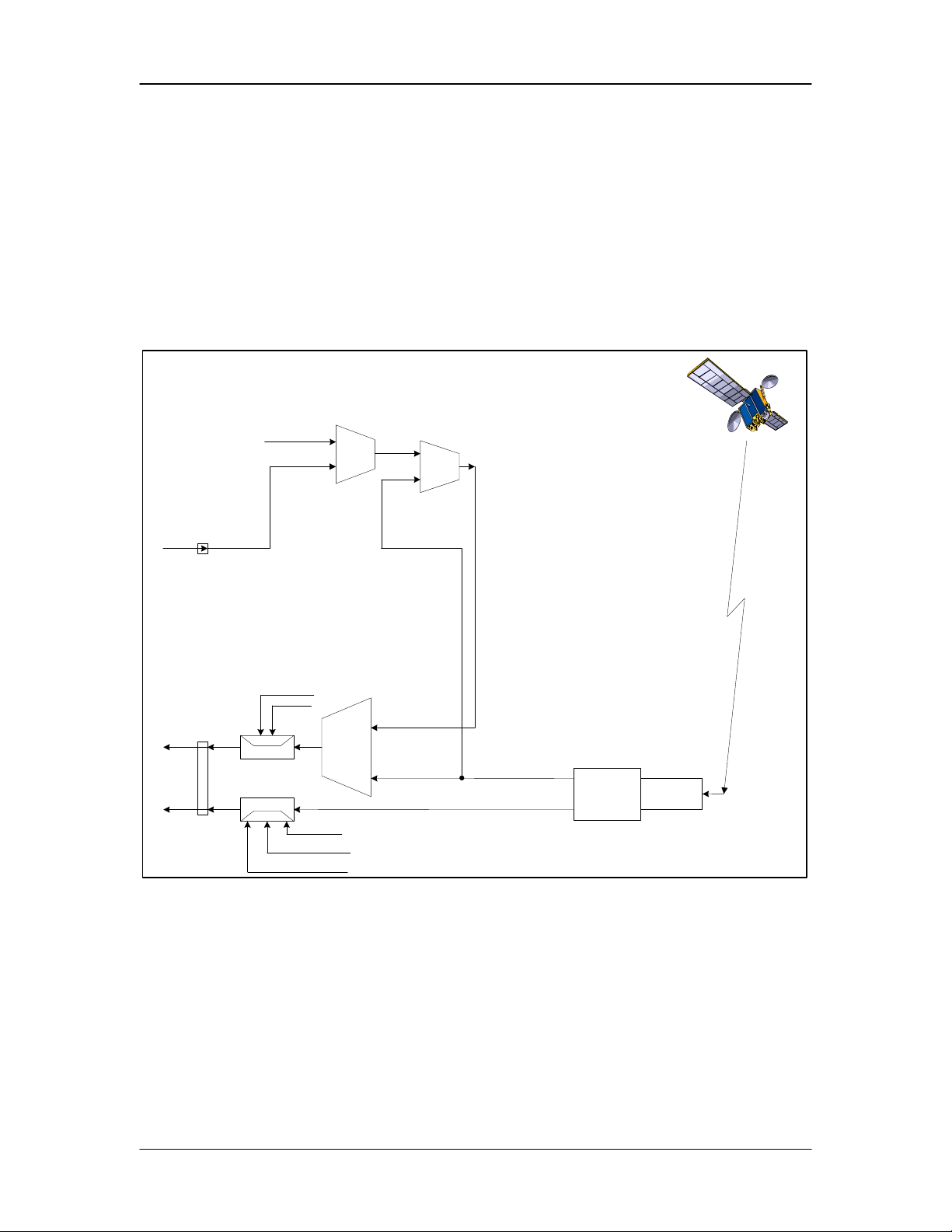
EXT REF
EXTERNAL
INTERNAL
SCT CLK
REF FREQ
SRC
RECEIVE
CLOCK & DATA
RECOVERY
SCT
RX SAT
RT
RD
BUFFER CLK
SRC
DEMODULATION
J19
J10
DATA POLARITY
BUFFER CLK POL
NORMAL
INVERTED
INVERT NONE
INV. BASEBAND
INV. TERR DATA
encoder which adds 2t = (N - K) check bytes to produce an N byte RS Block. The RS Decoder
can then correct up to “t” erred bytes in the block (refer to Figure 3-4 and Table 3-1).
3.2 Clocking Options
The Demodulator supports a number of different clocking options that can be recovered
from the satellite or the terrestrial links. The various clocking options allow users to
determine which clock will best fit their applications. Figure 3-7 gives an overview on
how the modem processes the various clocks for the Rx Buffer Clock source.
Figure 3-4. Clocking and Polarity Diagram
3.2.1 RX Buffer Clock Options
The modem supports a number of RX Buffer clock options that can be recovered from the
satellite, terrestrial links, internally or externally. The various clocking options allow users to
determine which clock will best fit their applications. Figure 3-7 gives an overview on how the
modem processes the various clocks for the Tx Clock and the Rx Buffer Clock. The modem
allows users to select clock polarity and Rx Clocks may be independently locked. The following
RX Buffer clock selections are available:
3-4 MN-VME2401 – Rev. B
Rx Satellite Clock (Recovered from Satellite)
Page 23
DD2401 VME L-Band Demodulator Card Installation & Operational Manual Theory of Operation
SCT (Internal Oscillator)
3.2.1.1 RX SAT Clock
The RX Sat clock is recovered from the satellite that is received from the distant end. If selected
the Buffer Clock is lock to the RX sat clock.
3.2.1.2 SCT: Serial Clo ck Tran sm it
If SCT clock is selected as the RX Buffer clock source, then it should be configured for internal.
SCT is sometimes referred to as Internal Timing or Send Timing (ST).
3.2.2 EXT REF: External Reference, J2
This is not actually a clock, but does have some clocking implications. When the external
reference is used, the master oscillator within the modem is locked to the external reference, and
the internal accuracy and stability of the unit assumes that of the External Reference. Therefore,
not only are the transmit frequencies locked to the external reference, but the modem’s internal
SCT Oscillator is locked to the external reference as well.
External reference port input is specified at 0 to +6 dBm.
3.2.2 Reed-Solomon Operation in the DD2401 VME Demodulator Card
When the Reed-Solomon Decoder is enabled, the signal is received and demodulated by the
receiving unit, fed to a Viterbi Decoder for the first layer of error correction. After error correction
by the Viterbi Decoder, the unique words are located and the data is deinterleaved and reformed
into blocks. The R-S Decoder then corrects the leftover errors in each block. The data is then
descrambled and output from the R-S Section.
3.2.3 Reed-Solomon Code Rate
The R-S Code Rate is defined by (N, K) where N is the total R-S block size in bytes (data + check
bytes) and K is the number of data bytes input into the R-S Encoder. The transmission rate
expansion required by the R-S Codec is then defined by N/K. The DD2401 VME
DEMODULATOR CARD allows any N or K setting up to N = 255, and K = 235 to allow tailoring of
the code rate to meet system requirements, with the following restrictions:
1. N/K must be less than 1.25 (25% maximum overhead).
2. N-K must be between 2 and 20, and must be even.
3. Maximum N = 255, Minimum N = 25.
4. Maximum K = 253, Minimum K = 23.
MN-VME2401 – Rev. B 3-5
Page 24
Theory of Operation DD2401 VME L-Band Demodulator Card Installation & Operational Manual
Small IDR
IDR
3.2.4 Interleaving
The DD2401 VME DEMODULATOR CARD allows for interleaving depths of 4 or 8 R-S blocks.
This allows burst errors to be spread over 4 or 8 R-S blocks in order to enhance the error
correcting performance of the R-S Codec.
Figure 3-4. Reed Solomon Decoder Functiona l Block Diagram
Table 3-1. Reed-Solomon Codes for IDR
Type of Service Data
Rate
(Kbps)
R-S Code
(n, k, t)1
Bandwidth
Expansion
[ (n/k) -1 ]
Interleaving
Depth
Maximum
R-S Codec
Delay (ms)
2
(with 16/15 O/H)
(with 96 Kbps O/H)
64
128
256
384
512
768
1024
1536
1544
2048
(126, 112, 7)
(126, 112, 7)
(126, 112, 7)
(126, 112, 7)
(126, 112, 7)
(126, 112, 7)
(126, 112, 7)
(126, 112, 7)
(225, 205,10)
(219, 201, 9)
0.125
0.125
0.125
0.125
0.125
0.125
0.125
0.125
0.0976
0.0896
4
4
4
4
4
4
4
4
4
4
115
58
29
19
15
10
8
5
9
7
n = code length, k = information symbo ls and t = symbol error correcting capability.
Design objective
For the DD2401 VME Demodulator Card, the IDR Deframing must be supplied externally.
3-6 MN-VME2401 – Rev. B
Page 25
DD2401 VME L-Band Demodulator Card Installation & Operational Manual User Interfaces
4
User Interfaces
4.0 User Interfaces
There are two user interfaces available for DD2401 VME Demodulator Card. These are:
a. Remote Port – (J5) Access to all available demodula tors
b. Terminal – (J1) Independent connection to each demodulator
4.1 Remote Port Control (J3)
All demodulators can be controlled by an external Monitor & Control (M&C) system through a
single Remote Port connection. Communication between the unit and the external system control
computer is via a binary protocol. The Remote Port provides RS-485 capability and thus is used
as a multi-drop control bus allowing a single external M&C computer to control all demodulators.
The Remote Port Data is outlined starting with Section 4.4 below.
4.2 Terminal Mode Control (J1)
Characters contained within the brackets < and > indicate pressing the appropr iate key.
The unit can be interactively monitored and controlled in the Terminal Mode, with a full screen
presentation of current settings and status. Programming is accomplished by selecting the item
to be modified and pressing the terminal key of the option number. For example, to change the
Receive Data Rate, enter “33” at the terminal. The DD240/VME2401/MD2401 DEMODULATOR
will respond by presenting the options available and requesting input. Two types of input may be
requested. If the input is multiple choice, the desired choice is selected by pressing <Space>.
When the desired option is displayed, press <Enter> to select that option. The other possible
input type requires a numerical input (such as entering a frequency or data rate). This type of
input is followed by pressing <Enter> or the carriage return key. An input can be aborted at any
time by pressing <ESC>. Invalid input keys cause an error message to be displayed on the
terminal.
The Terminal Control Mode supports a serial baud rate of 19200. The connection must be set for
8 data bits, 1 stop bit and no parity (8, N, 1). Three terminal emulations are supported: VT100,
WYSE 50, and ADDS. The emulation type can be changed by pressing <$> (dollar sign) on the
terminal keyboard.
MN-VME2401 – Rev. B 4-1
Page 26

User Interfaces DD2401 VME L-Band Demodulator Card Installation & Operational Manual
4.3 Terminal Port User Interface
Each demodulator has a Terminal Port Connection (J1) that allows for complete control and
monitoring of the demodulator parameters and functions via an RS-232 Serial Interface.
The factory default setup parameters are as follows:
Emulation Type: VT100 (can be changed)
Baud Rate: 19200
Data Bits: 8
Parity: No Parity (Fixed)
Stop Bits: 1 stop bit
4.3.1 Connecting the Terminal
1. Connect the computer to the Remote Connector (J5) on the rear of the unit using
the RS-232 Cable.
2. Enable the terminal by selecting Terminal Mode (located under the System Control Mode Menu) from the front panel.
3. Verify that your emulation software is set to the following:
8 data bits
no parity
1 stop bit
Modify the selection, if necessary, to match the settings (the Front Panel
‘SYSTEM’ Sub-Menu contains all the Terminal Emulation Controls).
4-2 MN-VME2401 – Rev. B
Page 27
DD2401 VME L-Band Demodulator Card Installation & Operational Manual User Interfaces
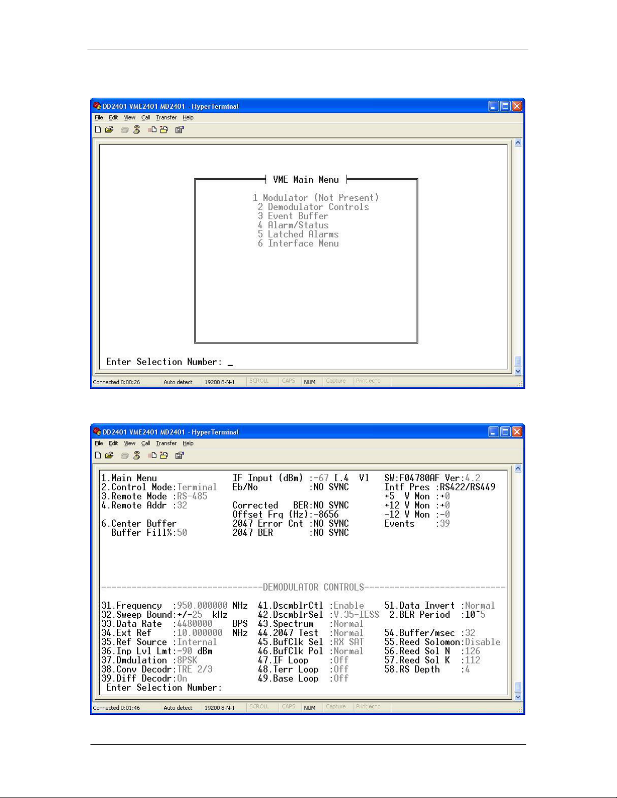
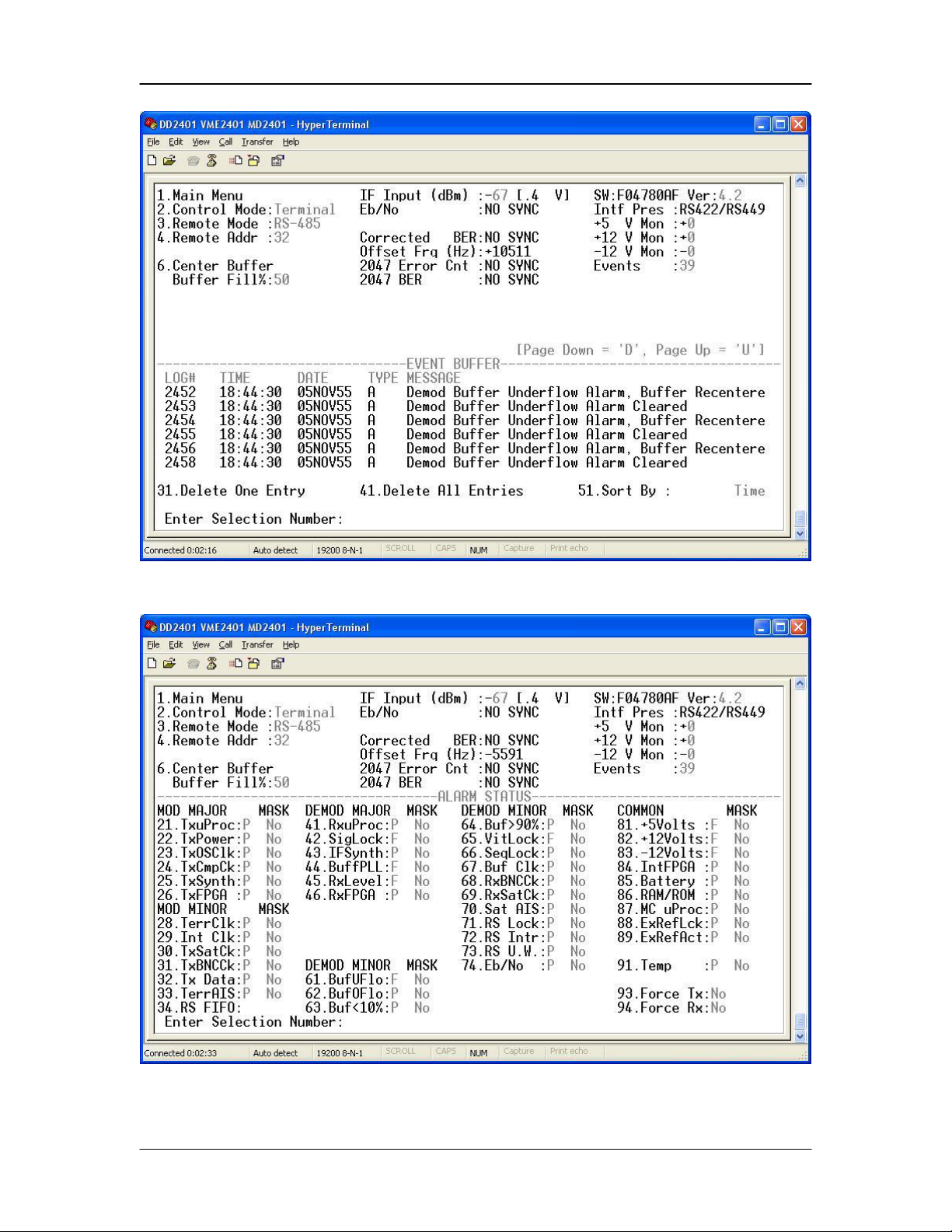
4.3.2 Terminal Screens
Figure 4-1. Main Menu
Figure 4-2. Demodulator Menu
MN-VME2401 – Rev. B 4-3
Page 28
User Interfaces DD2401 VME L-Band Demodulator Card Installation & Operational Manual
Figure 4-3. Event Buffer Menu
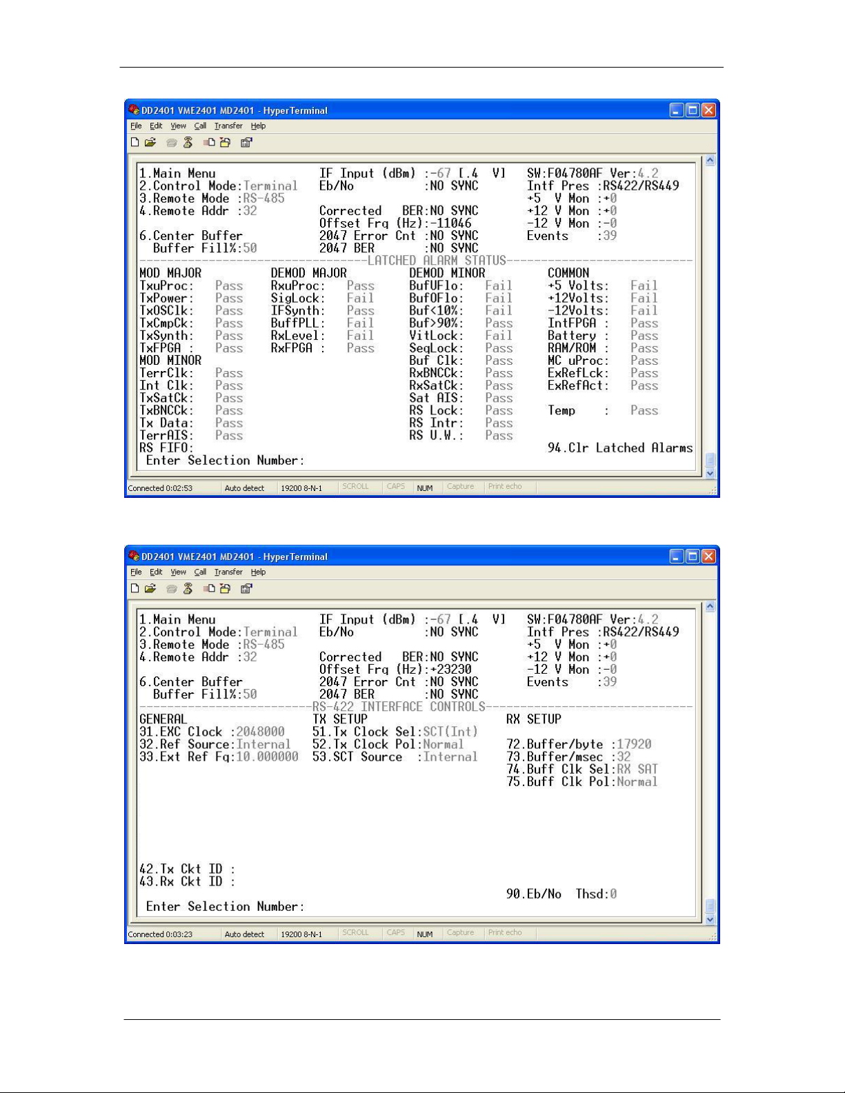
Figure 4-4. Alarm/Status Menu
4-4 MN-VME2401 – Rev. B
Page 29
DD2401 VME L-Band Demodulator Card Installation & Operational Manual User Interfaces
Figure 4-5. Latched Alarm Status Menu
Figure 4-6. Interface Controls Menu
MN-VME2401 – Rev. B 4-5
Page 30

User Interfaces DD2401 VME L-Band Demodulator Card Installation & Operational Manual
S1
S2
B0
B1
B2
B3
B4
B5
B6
B7
S1
S2, etc.
4.4 Remote Port User Interface
The Remote Port of the DD2401/DD2401L allows for complete control and monitor functions via
an RS-485 or RS-232 Internal Dip Switch Configurable Serial Interface.
Control and status m essages are conveyed between the DD2401/DD2401 L and the subsidiary
modems and the host computer using packetized message blocks in accordance with a
proprietary communications specification. This communication is handled by the Radyne Link
Level Protocol (RLLP), which serves as a protocol ‘wrapper’ for the M&C data.
Complete information on monitor and control software is contained in the following sections.
4.4.1 Protocol Structure
The Communications Specification (COMMSPEC) defines the interaction of computer resident
Monitor and Control software used in satellite earth station equipment such as Modems,
Redundancy Switches, Multiplexers, and other ancillary support gear. Communication is bidirectional, and is normally established on one or more full-duplex 9600-baud multi-drop control
buses that conform to EIA Standard RS-485. If a single device is placed on a single control bus,
then the control bus may conform to EIA Standard RS-232.
Each piece of earth s tation equipment on a c ontrol bus has a uni que physical addr ess, which is
assigned during stati on setup/config uration or prior t o shipm ent. Valid decim al addresses on one
control bus range from 032 to 255 for a tota l of up to 224 devices per bus. Addres s 255 of each
control bus is usually reserved for the M&C computer.
4.4.2 Protocol Wrapper
The Radyne COMMSPEC is byte-oriented, with the Least Significant Bit (LSB) issued first. Each
data byte is conveyed as mark/space information with one mark comprising the stop data. When
the last byte of data is transmitted, a hold comprises one steady mark (the last stop bit). To begin
or resume data transfer, a space (00h) substitutes this mark. This handling scheme is controlled
by the hardware and is transparent to the user. A pictorial representation of the data and its
surrounding overhead may be shown as follows:
The stop bit, S1 is a mark. Data flow remains in a hold mode until S1 is replaced by a space. If S1
is followed by a space, the space character is considered a start (ST ) and not part of the act ual
data (B
0 - B 7).
The above byte-oriented protocol is standard for UART based serial communication ports such as
Workstation or Persona l Computer (PC) COM por ts. COM ports should be conf igured for 8 data
bits, no parity, and one stop bit. For example, for 9600-baud operation, COM ports should be
configured as:
9600, 8, N, 1
The COMMSPEC developed for use with the Radyne Link Level Protocol (RLLP) organizes the
actual monitor and control data within a shell, or ‘protocol wrapper’, that surrounds the data. The
format and structure of the COMMSPEC message exchanges are described herein. Decimal
numbers have no suffix; hexadecimal numbers end with a lower case h suffix and binary values
have a lower case b suffix. Thus, 22 = 16h = 000010110b. The principal elements of a data
frame, in order of occurrence, are summarized as follows:
4-6 MN-VME2401 – Rev. B
Page 31

DD2401 VME L-Band Demodulator Card Installation & Operational Manual User Interfaces
Table 4-4. Checksum Calculation Example
Byte Field
Data Content
Running Checksum
<BYTE COUNT> (Byte 1)
00h = 00000000b
00000000b
<BYTE COUNT> (Byte 2)
02h = 00000010b
00000010b
<SOURCEID>
F0h = 11110000b
11110010b
<DESTINATION ID>
2Ah = 00101010b
00011100b
<FSN>
09h = 00001001b
00100101b
<OPCODE> (Byte 1)
00h = 00000000b
00100101b
<OPCODE> (Byte 2)
03h = 00000011b
00101000b
<DATA> (Byte 1)
DFh = 11011111b
00000111b
<DATA> (Byte 2)
FEh = 11111110b
00000101b
<SYNC> - the message format header character, or ASCII sync character, that defines the
beginning of a message. The <SYNC> character value is always 16h (1 Byte).
<BYTE COUNT> - the Byte Count is the number of bytes in the <DATA> field (two bytes).
<SOURCE ID > - the Source Identifier def ines the multi-drop address or igin. Note that all nodes
on a given control bus have a unique address that must be defined (1 Byte).
<DESTINATION ID> - The Destinati on Identifier ser ves as a po inter to the multi-drop destin ation
device that indicates where the message is to be sent (1 Byte).
<FRAME SEQU ENCE N UMBER> -The FSN is a tag with a val ue from 0 thr ough 255 t hat is sent
with each mess age. It assures sequential information framing and correct equipm ent
acknowledgment and data transfers (1 Byte).
<OPCODE> - The Operation Code field contains a number that identifies the message type
associated with the d ata that follows it. Equi pment under MCS control rec ognizes this
code via firmware identification and subsequently steers the DATA accordingly to
perform a specific function or series of functions. Ack nowledgm ent and error code s are
returned in this field (two bytes).
<...DATA...> - T he Data f ield cont ains the bi nary data bytes associated wit h the <O PCO D E>. Th e
number of data bytes in this field is indicated by the <BYTE COUNT> value.
<CHECKSUM> - The checksum is the modulo 256 sum of all preceding message bytes,
excluding the <SYNC> cha racter (1 Byte). The checksum determ ines the presence or
absence of errors within the message. In a message block with the following
parameters, the checksurn is computed as shown in Table 4-4 below.
Thus, the checksum is 00000101b; which is 05h or 5 decimal. Alternative methods of calculating
the checksum for the same message frame are:
Since the only concern is the modulo 256 (modulo 1 00h) equivalent (values that can be
represented by a single 8-bit byte), the checksum is 05h.
For a decimal checksum calculation, the equivalent values for each information field are:
MN-VME2401 – Rev. B 4-7
00h + 02h + F0h + 2Ah + 09h + 00h + 03h + DFh + FEh = 305h.
0 + 2 + 240 + 42 + 9 + 0 + 3 + 223 + 254 = 773;
773/256 = 3 with a remainder of 5.
This remainder is the checksum for the frame.
5 (decimal) = 05h = 0101b = <CHECKSUM>
Page 32

User Interfaces DD2401 VME L-Band Demodulator Card Installation & Operational Manual
4.4.3 Frame Description and Bus Handshaking
In a Monitor and Control environment, every message frame on a control bus port executes as a
packet in a loop beginning with a wait-for-SYNC-character mode. The remaining message format
header information is then loaded, either by the M&C computer or by a subordinate piece of
equipment (such as the DD2401/DD2401L) requesting access to the bus. Data is processed in
accordance with the OPCODE, and the checksum for the frame is calculated. If the anticipated
checksum does not match then a checksum error response is returned to the message frame
originator. The entire message frame is discarded and the wait-for-SYNC mode goes back into
effect. If the OPCODE resides within a command message, it defines the class of action that
denotes an instruction that is specific to the device type, and is a prefix to the DATA field if data is
required. If the OPCODE resides within a query message packet, then it defines the query code,
and can serve as a prefix to query code DATA.
The Frame Sequence Number (FSN) is included in every message packet, and increments
sequentially. W hen the M&C computer or bus-link ed equipment initiates a message, it assigns
the FSN as a tag for error control and handshaking. A different FSN is produced f or each new
message from the F SN ori ginator to a spec ific device on the contro l bus. If a com mand pack et is
sent and not recei ved at its intended desti nation, then an appropr iate response message is not
received by the pack et originator. The original command pack et is then re-transmitted with the
same FSN. If the repeated message is received correctly at this point, it is considered a new
message and is executed and acknowledged as such.
If the command packet is received at its intended destination but the response message
(acknowledgment) is lost, then the message originato r (usually the M&C computer) r e-transmits
the original command pac ket with the same FSN. T he destination device detec ts the same FSN
and recognizes that the m essage is a duplicate, so the ass ociated commands within the pac ket
are not executed a second tim e. However, the response pac ket is again sent back to the s ource
as an acknowledgment in order to preclude undesired multiple executions of the same command.
To reiterate, valid equipment responses to a message require the FSN tag in the command
packet. This serves as par t of the handshake/acknowledge rou tine. If a valid response mes sage
is absent, then the command is re-transmitted with the same FSN. For a repeat of the same
command involving iterative processes, the FSN is incremented after each message packet.
When the FSN value reaches 255, it overflows and begins again at zero. The FSN tag is a
powerful tool that assures sequential information framing, and is especially useful where
commands require more than one message packet.
The full handshake/acknowledgment involves a reversal of source and destination ID codes in the
next message frame, followed by a response code in the <OPCODE> field of the message
packet from the equipment under control.
If a command pack et is s ent and not receive d at its in tended des tination , a tim eout condition can
occur because the pac k et origi nator do es n ot rec eive a respo nse m es sage. On r ecei ving d evices
slaved to an M&C computer, the timeout delay parameters may be programmed into the
equipment in accordance with site requirements by Comtech EF Data prior to shipment, or
altered by qualified person nel. T he FSN hands hak e routines m ust account f or tim eout dela ys and
be able to introduce them as well.
4.4.4 Globa l Response Operational Codes
In acknowledgment (response) packets, the operational code <OPCODE> field of the message
packet is set to 0 by the receiving devices when the message intended for the device is evaluated
as valid. The device that receives the valid message then exchanges the <SOURCE ID> with the
<DESTINATION ID>, sets the <OPCO D E> to zero in order to indicate that a good message was
received, and returns the packet to the originator. This “GOOD MESSAGE” opcode is one of nine
global responses. Global response opcodes are common responses, issued to the M&C
4-8 MN-VME2401 – Rev. B
Page 33

DD2401 VME L-Band Demodulator Card Installation & Operational Manual User Interfaces
Table 4-5. Response Opcodes
Response Opcode Description
Opcode
Good Message
0000h
Bad Parameter
00FFh
Bad Opcode
00FEh
Bad Checksum
00FDh
Command Not Allowed in LOCAL Mod e
00FCh
Command Not Allowed in AUTO Mode
00FBh
Bad Destination
00FAh
Unable to Process Command
00F9h
Packet Too Long
00F8h
Response Opcode Description
Opcode
DPARM_MODE_ERROR
0x0600
DPARM_FREQUENCY_ERROR
0x0601
DPARM_DATARATE_ERROR
0x0603
DPARM_SWEEPBOUNDARY_ERROR
0x0604
DPARM_LEVELLIMIT_ERROR
0x0605
DPARM_DEMODULATIONTYPE_ERROR
0x0608
DPARM_CONVDECODER_ERROR
0x0609
DPARM_REEDSOLOMON_ERROR
0x060A
DPARM_DIFFERENTIALDECODER_ERROR
0x060B
DPARM_DESCRAMBLERCONTROL_ERROR
0x060C
DPARM_DESCRAMBLERTYPE_ERROR
0x060D
DPARM_SPECTRUM_ERROR
0x060E
DPARM_BUFFERCLOCK_ERROR
0x0610
DPARM_BUFFERCLOCKPOL_ERROR
0x0611
DPARM_INSERTMODE_ERROR
0x0612
DPARM_FRAMING_ERROR
0x0615
DPARM_OPERATINGMODE_ERROR
0x0616
DPARM_BERMEASUREPERIOD_ERROR
0x0619
DPARM_CIRCUITID_ERROR
0x061A
DPARM_TERRLOOPBACK_ERROR
0x061B
DPARM_BASELOOPBACK_ERROR
0x061C
DPARM_IFLOOPBACK_ERROR
0x061D
DPARM_INTERFACETYPE_ERROR
0x061E
DPARM_NOTIMPLEMENTED_ERROR
0x0622
DPARM_DATAINVERT_ERROR
0x0623
DPARM_SUMMARYFAULT_ERROR
0x0624
DPARM_EXTERNALEXCSOURCE_ERROR
0x0625
DPARM_BUFFERSIZEMSEC_ERROR
0x0629
DPARM_BUFFERSIZEBYTES_ERROR
0x062A
DPARM_ASYNCINTERFACETYPE_ERROR
0x0630
DPARM_BUFFERSIZEMSECBYTES_ERROR
0x0631
DPARM_IMPEDANCE_ERROR
0x0632
DPARM_INTERLEAVER_ERROR
0x0635
MDPARM_TIME_ERROR
0x0A01
MDPARM_DATE_ERROR
0x0A02
computer or to another device, that can originate from and are interpreted by all Radyne
equipment in the same manner. These are summarized as follows (all opcode values are
expressed in decimal form):
The following response error codes are specific to the DD2401/DD2401L:
MN-VME2401 – Rev. B 4-9
Page 34

User Interfaces DD2401 VME L-Band Demodulator Card Installation & Operational Manual
Directly-Addressed Equipment
Multi-Drop
Override ID
Broadcast (all directly-linked devices)
00
DMD-3000/4000, 4500 or 5000 Mod Section, DMD15
01
DMD-3000/4000, 4500 or 5000 Demod Section, DMD15
02
RCU-340 1:1 Switch
03
RCS-780 1:N Switch
04
RMUX-340 Cross-Connect Multip lexer
05
CDS-780 Clock Distribution System
06
SOM-340 Second Order Multiplexer
07
DMD-4500/5000 Modulator Section
08
DMD-4500/5000 Demodulator Section
09
RCU-5000 M:N Switch
10
DMD15 Modulator
20
DMD15 Demodulator
21
DMD15 Modem
22
DVB3000/DVB3030/DM45/DM240 Video Modulator
23
RCS20 M:N Switch
24
RCS10 M:N Switch
25
RCS11 1:1 Switch
26
DD2401/DD2401L Demodulator
27
Reserved For Future Equipment Types
28-31
4.4.5 Collis ion Avoidance
When properly implemented, the physical and logical devices and ID addressing scheme of the
COMMSPEC normally precludes message packet contention on the control bus. The importance
of designating unique IDs for each device during station configuration cannot be overemphasized.
One pitfall, which is often overlooked, concerns multi-drop override IDs. All too often, multiple
devices of the same type are assigned in a direct-linked (“single-thread”) configuration accessible
to the M&C computer directly. For example, if two DD2401/DD2401L Demodulators with different
addresses (DESTINATION IDs) are linked to the same control bus at the same hierarchical level,
both will attempt to respond to the M&C computer when the computer generates a multi-drop
override ID of 22. If their actual setup parameters, status, or internal timing differs, they will both
attempt to respond to the override simultaneously with different information or as ync hrono us l y in
their respective message packets and response packets, causing a collision on the serial control
bus.
To preclude control bus data c ontention , diff erent IDs m ust always be ass igned t o the equipm ent.
If two or more devices are c onfigured for direct-linked operation, then the M&C computer and al l
other devices configured in the same manner must be programmed to inhibit broadcast of the
corresponding multi-drop override ID.
The multi-drop o verride I D is al ways acc epted b y devices of the s ame t ype on a c omm on control
bus, independent of the actual DESTINATION ID. These override IDs with the exception of
“BROADCAST” are responded to by all directly linked devices of the same type causing
contention on the bus. The “ BROADCAST” ID, on the other hand, is ac cepted by all equipment
but none of them returns a response packet to the remote M&C.
The following multi-drop override IDs are device-type specific, with the exception of
“BROADCAST”. These are summarized below with ID values expressed in decimal notation:
Note that multi-drop override IDs 01 or 02 can be used interchangeably to broadcast a message
to a DMD3000/4000 modem, or to a DMD4500/5000, or to a DMD15 modem. Comtech EF Data
recommends that the multi-drop override IDs be issued only during system configuration as a bus
4-10 MN-VME2401 – Rev. B
Page 35

DD2401 VME L-Band Demodulator Card Installation & Operational Manual User Interfaces
test tool by experienced programmers, and that they not be included in run-time software. It is
also advantageous to consider the use of multiple bus systems where warranted by a moderate
to large equipment complement. Therefore, if a DD2401/DD2401L is queried for its equipment
type identifier, it will return a “27”.
4.4.6 Software Compatibility
The DD2401/DD2401L RLLP is not software-compatible with the following
previous Radyne products: RCU5000 and DMD4500. These products may not
occupy the same bus while using this protocol as equipment malfunction and
loss of data may occur.
When Radyne equipm ent is queried f or inform ation (Query Mod, Query Demod, etc.) it responds
by sending back two blocks of data; a non-vol atile section (parameters that c an be modified by
the user) and a volati le section (status information). I t also returns a count value that indicat es
how large the non-vol atile section is. This count is us e d b y M&C de vel o pers to i n dex int o th e s tart
of the volatile section.
When new features are added to Rad yne equ ipm ent, the contro l param eters are appende d to the
end of the non-volatile section, and status of the f eatures, if any, are added at the end of the
volatile sect ion. If a r emote M&C queri es two piec es of R adyne equipm ent with diff erent sof tware
revisions, they m ight res p o nd with two different sized pac kets. The remote M&C MUST make use
of the non-volatile count va l ue to ind ex to th e s tart of the volatile section. If the r em ote M &C is not
aware of the newl y added features to the Rad yne product, it sh ould disregard t he parameter s at
the end of the non-volatile section and index to the start of the volatile section.
If packets are handled in this fashion , there will als o be backward-c ompatibility bet ween Radyne
equipment and M&C syste ms. Remote M&C systems need not be m odified every time a feature
is added unless the user needs access to that feature.
4.4.7 Flow Control and Task Processing
The original packet sender (the M&C computer) relies on accurate timeout information with
regard to each piece of equipment under its control. This provides for efficient bus communication
without unnecessary handshake overhead timing. One critical value is designated the InterFrame Space (FS). The Inter-Frame Space provides a period of time in which the packet receiver
and medium (control bus and M&C computer interface) fully recover from the packet
transmission/reception process and the receiver is ready to accept a new message. The
programmed value of the Inter-Frame Space should be greater than the sum of the “turnaround
time” and the round-trip (sender/receiver/bus) propagation time, including handshake overhead.
The term “turnaround time” refers to the amount of time required for a receiver to be re-enabled
and ready to receive a packet after having just received a packet. In flow control programming,
the Inter-Frame Space may be determined empirically in accord with the system configuration, or
calculated based on established maximum equipment task processing times.
Each piece of supported equipment on the control bus executes a Radyne Link Level Task
(RLLT) in accordance with its internal hardware and fixed program structure. In a flow control
example, the RLLT issues an internal “message in” system call to invoke an I/0 wait condition that
persists until the task receives a command from the M&C computer. The RLLT has the option of
setting a timeout on the incoming message. Thus, if the equipment does not receive an
information/command packet within a given time period, the associated RLLT exits the I/0 wait
state and takes appropriate action.
MN-VME2401 – Rev. B 4-11
Page 36

User Interfaces DD2401 VME L-Band Demodulator Card Installation & Operational Manual
Table 4-6. Link Level Protocol Message Block
SYNC
COUNT
SOURCE
DESTINATION
FSN
OPCODE
DATA
CHECKSUM
Radyne equipment is logically linked to the control bus via an Internal I/O Processing Task (IOPT)
to handle frame sequencing, error checking, and handshaking. The IOPT is essentially a link
between the equipment RLLT and the control bus. Each time the M&C computer sends a
message packet, the IOPT receives the message and performs error checking. If errors are
absent, the IOPT passes the message to the equipment’s RLLT. If the IOPT detects errors, it
appends error messages to the packet. Whenever an error occurs, the IOPT notes it and discards
the message; but it k eeps track of the incom ing packet. Once the pack et is complete, the IOPT
conveys the appropriate message to the RLLT and invokes an I/0 wait state (wait for next
<SYNC> character).
If the RLLT recei ves the packetized mes sage from the sender before it times out, it checks f or
any error messages appen ded by the IOPT. In the absence of errors, the RLLT processes the
received command sent via the transmitted packet and issues a “message out” s ystem call to
ultimately acknowledge the received packet. This call generates the response packet conveyed to
the sender. If the IOPT sensed errors in the received packet and an RLLT timeout has not
occurred, the RLLT causes the equipment to issue the appropriate error message(s) in the
pending equipment response frame.
To maintain frame synchronization, the IOPT keeps track of error-laden packets and packets
intended for other equipment for the duration of each received packet. Once the packet is
complete, the IOPT invokes an I/0 wait state and searches for the next <SYNC> char act er.
4.4.8 RLLP Summ ary
The RLLP is a simple send-and-wait protocol that automatically re-transmits a packet when an
error is detected, or when an acknowledgment (response) packet is absent.
During transmiss ion, the protocol wrapper surrounds t he actual data to form information pack ets.
Each transmitted packet is subject to time out and frame sequence control parameters, after
which the packet s ender waits for the receiver to con vey its response. Once a recei ver verifies
that a packet sent to it is in the correct sequence relative to the previously received pack et, it
computes a local chec ksum on all inform ation within the pack et excluding t he <SYNC> c haracter
and the <CHECKSUM > fiel ds. If this c heck sum m atches the pack et <CHEC KSUM>, the recei ver
processes the packet and responds to the packet sender with a valid response (acknowledgment)
packet. If the checksum values do not match, the receiver replies with a negative
acknowledgment (NAK) in its response frame.
The response packet is therefore either an acknowledgment that the message was received
correctly, or some form of a packetized NAK frame. If the sender receives a valid
acknowledgment (res pons e ) packet from the receiver, the <FS N> inc r ements and the next packet
is transmitted as required by the sender. However, if a NAK response packet is returned, the
sender re-transmits the original information packet with the same embedded <FSN>.
If an acknowledgment ( response) packet or a NAK packet is lost, cor rupted, or not issued du e to
an error and is thereby not r eturned to the sender, the s ender r e-transmits the origina l inf ormation
packet; but with the sam e <FSN>. When the intended recei ver detects a duplicate packet, the
packet is acknowled ged with a response pack et and internally discarded to preclude undesired
repetitive executions. If the M&C computer sends a command packet and the corresponding
response packet is lost due to a s ystem or intern al err or, the c om puter tim es out and r e-transmits
the same command packet with the same <FSN> to the sam e receiver and waits once again for
an acknowledgment or a NAK packet.
To reiterate, the form at of the message block is shown in T able B -4 , Li nk Level Protocol Message
Block.
4-12 MN-VME2401 – Rev. B
Page 37

DD2401 VME L-Band Demodulator Card Installation & Operational Manual User Interfaces
ADDRESS
ADDRESS
BYTES
RLLP Command
Opcode
Query Demodulator All
2401h
Query Demod Latched Alarms
2406h
Query Demod Current Alarms
2409h
Query Demod Status
240Ch
Query Demod Eb/No, Input Level, Raw BER, Corrected
BER, and Frequency Offset, AGC Voltage
240Dh
Query Demod Lock Status
2437h
Command Demod All
2A00h
Command Demod Frequency
2A01h
Command Demod Data Rate
2A02h
Command Demod Sweep Boundary
2A04h
Command Demod Demodulation Type
2A07h
Command Demod Convolutional Decoder
2A08h
Command Demod Differential Decoder
2A09h
Command Demod Reed-Solomon
2A0Ah
Command Demod Descrambler
2A0Dh
Command Demod Descrambler Type
2A0Eh
Command Demod Spectrum
2A0Fh
Command Demod Buffer Clock
2A11h
Command Demod Buffer Clock Polarity
2A12h
The RLLP Remote Port Packet structure is as follows:
<SYNC> Message format header character that defines the beginning of a
message. The <SYNC> character value is always 0x16. (1 byte)
<BYTE COUNT> Number of bytes in the <DATA> field. (2 bytes)
<SOURCE ADDR> Identifies the address of the equipment from where the message
originated. (1 byte)
<DEST ADDR> Identifies the address of the equipment where the message is to be sent.
(1 byte)
<FSN> Frame sequence number ensures correct packet acknowledgment and data
transfers. (1 byte)
<OPCODE> This byte identifies the message type associated with the information
data. The equipment processes the data according to the value in this field. Return error
codes and acknowledgment are also included in this field. (2 bytes)
<...DATA...> Information data. The number of data bytes in this field is indicated by
the <BYTE COUNT> value.
<CHECKSUM> The modulo 256 sum of all preceding message bytes excluding the
<SYNC> character. (1 byte)
4.4.9 DD2401/DD2401L Opcode Command Set
The DD2401/DD2401L Opcode Command Set is listed below, separated by commands that
control the demodulator, or the entire module.
4.4.10 Demodulator Command Set
MN-VME2401 – Rev. B 4-13
Page 38

User Interfaces DD2401 VME L-Band Demodulator Card Installation & Operational Manual
Command Demod Operating Mode
2A17h
Command Demod BER Measure Period
2A1Ah
Command Demod Terrestrial Loopback
2A1Ch
Command Demod Baseband Loopback
2A1Dh
Command Demod Center Buffer
2A20h
Command Demod Data Invert
2A21h
Command Demod Buffer Size Time/Bytes
2A31h
RLLP Command
Opcode
Query Module Identification
2403h
Query Module Current Alarms
240Ah
Query Module Time
240Eh
Query Module Date
240Fh
Query Module Time and Date
2410h
Command Module Control Mode
2600h
Command Module Ext Ref Source
2616h
Command Mod Ext Ref Frequency
261Bh
Command Module Clear Latched Alarms
2C03h
Command Module Set Time
2C04h
Command Module Set Date
2C05h
Command Module Set Time and Date
2C06h
Command Module Soft Reset
2C07h
Command Module Eb/No Threshold
2C08h
Command Module Default Configuration
2C30h
Query Response
<1>
Number of Nonvol
and is an offset to the start of the status block.
Configuration Bytes
<4>
Frequency
Binary Value, 1 Hz Steps
4.4.11 Module Command Set
1
Applies to base band frequency modems only.
2
Applies to LB/ST modem configurations only.
4.4.12 Detailed Command Descriptions
4.4.12.1 DMD2401 Demodulator
Note: All bytes preceded by a * are not applicable to the DD2401/DD2401L and should be considered
as reserved and there returned values ignored.
Opcode: <2401h> Query a Demodulator’s Configuration and Status
<4>
<1>
<4>
bytes
Data Rate
Sweep Boundary
External
Reference
See Paragraph B.6. This is the number of configuration bytes
Binary Value, 1 bps Steps
Sweep Limits (Max of ± 42 kHz)
Unsigned Binary Value in Hz
4-14 MN-VME2401 – Rev. B
Page 39

DD2401 VME L-Band Demodulator Card Installation & Operational Manual User Interfaces
<1>
<1>
Freq. Reference
Alarm 2 Mask
0 = Internal, 1 = External
Bit 0 = Buffer Underflow
<1>
<1>
<1>
<1>
<1>
<1>
<1>
<1>
<1>
<1>
<1>
<1>
<4>
<1>
<1>
<1>
<1>
Source
Input Level Limit
Demodulation
Type
Convolutional
Decoder
Reed-Solomon
Reed-Solomon N
Reed-Solomon K
Reed-Solomon T
RS Interleaver
Depth
Differential
Decoder
Descrambler
Control
Descrambler Type
Spectrum
Buffer Size
Buffer Clock
Buffer Clock
Polarity
Operating Mode
Alarm 1 Mask
Lower Level Limit, Binary Value, 1 dB Steps, Negative Sign Implied
0 = QPSK, 1 = BPSK, 2 = 8PSK, 4 = OQPSK
0 = None, 1 = Viterbi 1/2 Rate, 3 = Viterbi 3/4 Rate, 5 = Viterbi 7/8
Rate, 7 = Sequential 1/2 Rate, 9 = Sequential 3/4 Rate, 11 =
Sequential 7/8 Rate, 14 = Trellis 2/3, 20 = TPC 0.793 2D, 21 = TPC
0.495 3D, 23 = TPC ½, 24 = TPC ¾, 25 = TPC 7/8, 26 = TPC 21/44
0 = Disable, 1 = Enable
Unsigned Binary
Unsigned Binary
Unsigned Binary
Unsigned Binary, 4 or 8
0 = Off, 1 = On
0 = Disable, 1 = Enable
0 = None, 1 = IBS Scrambler, 2 = V35_IESS, 3 = V35_CCITT, 4 =
V35_EFDATA, 6 = OM73, 7 = Reed-Solomon Scrambler, 8 =
V35_EFRS, 9 = TPC Scrambler
0 = Normal, 1 = Inverted
Byte 1 - 2 = Buffer Size in ms
Byte 3 - 4 = Buffer Size in Bytes
0 = External, 1 = Internal, 2 = EXC, 3 = RX SAT
0 = Normal, 1 = Inverted
0 = Normal, 1 = 2047 Test
Bit 0 = Receive Processor Fault
Bit 1 = Signal Lock Fault
Bit 2 = Receive Satellite AIS Fault
Bit 3 = Rx AGC/Input Level Fault
Bit 4 = Reed-Solomon Sync Fault
Bit 5 = Reed-Solomon Excessive Errors Fault
Bit 6 = Reed-Solomon Uncorrectable Word Fault)
Bit 7 = Receive Forced Alarm
(0 = Mask, 1 = Allow)
MN-VME2401 – Rev. B 4-15
Page 40

User Interfaces DD2401 VME L-Band Demodulator Card Installation & Operational Manual
Bit 1 = Buffer Overflow
<1>
<1>
<1>
<1>
<1>
<24>
<1>
<1>
*<1>
<1>
<1>
Alarm 3 Mask
Alarm 4 Mask
Common Alarm 1
Mask
Reserved
BER Measure
Period
Rx Circuit ID
Rx Terrestrial
Loopback
Rx Baseband
Loopback
Rx IF Loopback
Reserved
Data Invert
Bit 2 = Buffer Under 10%
Bit 3 = Buffer Over 90%
Bit 4 = Receive FPGA Configuration Alarm Fault
Bit 5 = Rx LNB Fault, LBST Only
Bits 6 - 7 = Spares
(0 = Mask, 1 = Allow)
Bit 0 = IF Synthesizer Lock Detect Fault
Bit 1 = Rx Oversample PLL Lock Detect Fault
Bit 2 = Buffer Clock PLL Lock Detect Fault
Bit 3 = Viterbi Decoder Lock Fault
Bit 4 = Sequential Decoder Lock Fault
Bit 5 = Rx 2047 Test Pattern Lock Fault
Bit 6 = External Reference PLL Lock Fault
Bit 7 = Frame Sync/Multiframe Sync Loss
(0 = Mask, 1 = Allow)
Bit 0 = Buffer Clock Activity Detect Fault
Bit 1 = External BNC Activity Detect Fault
Bit 2 = Rx Satellite Clock Activity Detect Fault
Bit 3 = External Reference PLL Activity Fault
Bit 4 = High Stability Activity Detect Fault
Bit 5 = High Stability PLL Fault
Bit 6 = Eb/No Threshold Fault
Bit 7 = Spare
(0 = Mask, 1 = Allow)
Bit 0 = -12 V Alarm
Bit 1 = +12 V Alarm
Bit 2 = +5 V Alarm
Bit 3 = Temperature
Bit 4 = Interface FPGA Fault
Bit 5 = Battery Fault
Bit 6 = RAM/ROM Fault
Bit 7 = Spare
(0 = Mask, 1 = Allow)
Set to Zero
Unsigned Binary Number of Bits in Measur ement Period, in Powers
of Ten (ex: 6 = 10
6
Bits)
24 ASCII Characters
0 = Disabled, 1 = Enabled
0 = Disabled, 1 = Enabled
0 = Disabled, 1 = Enabled
Ignore
0 = Normal, 1 = Invert
4-16 MN-VME2401 – Rev. B
Page 41

DD2401 VME L-Band Demodulator Card Installation & Operational Manual User Interfaces
Note: The following byte applies o n ly if an Asynchronous, IDR
*<1>
*<1>
*<1>
*<1>
*<1>
*<1>
<1>
<1>
*<1>
Async Framing
Async Baud Rate
Async Port Type
Async Terrestrial
Interface Type
Multiprotocol
Interface Card
Interface Type
G.703 Interface
Type
BPSK Symbol
Pairing
Receive Mode
T1/E1 Frame
Source
or IBS Interface is installed. If not, ignore.
0 = No Framing, 1 = 1/16 Async, 2 = 1/16 IBS, 3 = 96 Kbit IDR
Note: The following byte applies o n ly if an asynchronous
interface card is installed. If no t, ignore.
0 = 1200, 1 = 2400, 2 = 4800, 3 = 9600, 4 = 19200, 5 = 50, 6 = 110,
7 = 300, 8 = 600
Note: The following byte applies o n ly if an asynchronous
interface card is installed. If no t, ignore.
0 = RS-232, 1 = RS-485
Note: The following byte applies o n ly if an asynchronous
interface card is installed. If no t, ignore.
0 = V.35, 1 = RS-422, 2 = RS-232
Note: The following byte applies o n ly if a synchronous
Multiprotocol interface card is installed. If not, ignore.
0 = V.35, 1 = RS-422, 2 = RS-232
Note: The following byte applies o n ly if a symmetric G.703
interface card is installed. If no t, ignore.
0 = G703T1AMI, 1 = G703T1B8ZS, 2 = G703BE1, 3 = G703UE1
Note: The following byte applies to all DMD2401 modems,
regardless of interface type.
0 = Normal, 1 = Swapped
Note: The following byte applies o n ly if an IDR OR IBS
interface card is installed. If no t, ignore.
0 = Closed Net Mode, 1 = IDR Mode, 2 = IBS Mode, 3 = D&I Mode
Note: The following byte applies o n ly if an IDR OR IBS
interface card is installed and the Receive Mode is set to
IDR Mode. If not, ignore
0 = Internal, 1 = External
Note: The following byte applies o n ly if an IDR OR IBS
interface card is installed and the Receive Mode is set to
IDR Mode. If not, ignore
MN-VME2401 – Rev. B 4-17
Page 42

User Interfaces DD2401 VME L-Band Demodulator Card Installation & Operational Manual
*<1>
Receive IDR
0 = Voice, 1 = 64 K Data
*<1>
*<1>
*<2>
*<2>
*<1>
*<1>
*<30>
*<1>
Overhead Mode
Receive IDR / IBS
Backward Alarms
Mask
Interface Type
Receive ESC
Audio #1 Volume
Receive ESC
Audio #2 Volume
Alarm 5 Mask
Insert Mode
Insert Map
Insert Alarm Mask
Note: The following byte applies o n ly if an IDR OR IBS
interface card is installed and the Receive Mode is set to
IDR Mode. If not, ignore
Bit 0 = IDR Backward Alarm 1 / IBS Backward Alarm
Bit 1 = IDR Backward Alarm 2
Bit 2 = IDR Backward Alarm 3
Bit 3 = IDR Backward Alarm 4
Bits 4 - 7 = Spares
(0 = Mask, 1 = Allow)
Note: The following byte applies o n ly if an IDR OR IBS
interface card is installed and the Receive Mode is set to
IDR Mode. If not, ignore
If G.703 Daughter Card Installed
0 = G.703 Unbalanced E1, 1 = G.703 Balanced E1, 2 = G.703 T1,
B8ZS
If synchronous Multiprotocol daug h ter card is installed:
0 = V.35, 1 = RS-422, 2 = RS-232
Note: The following two bytes apply only if an IDR OR IBS
interface card is installed and the Receive Mode is set to IDR
Mode. If not, ignore
-20 to +10, Signed Binary Value in dB
Note: The following two bytes apply only if an IDR OR IBS
interface card is installed and the Receive Mode is set to IDR
Mode. If not, ignore
-20 to +10, Signed Binary Value in dB
Bit 0 = IBS Satellite Multiframe Fault
Bit 1 = IBS Satellite Frame Fault
Bit 2 = Spare
Bit 3 = IBS Alarm if BER < 10-03
Bit 4 = IBS Prompt Alarm
Bit 5 = IBS Service Alarm
Bit 6 = Turbo Codec Lock Fault
Bit 7 = Spare
(0 = Mask, 1 = Allow)
0 = Disable, 1 = T1-D4, 2 = T1-ESF, 3 = PCM-30, 4 = PCM-30C, 5 =
PCM-31, 6 = PCM-31C, 7 = T1-SLC96, 8 = T1-D4-S, 9 = T1-ESF-S
Mapping of Satellite Channels to insert Terrestrial Timeslots
Bit 0 = Frame Lock Fault
4-18 MN-VME2401 – Rev. B
Page 43

DD2401 VME L-Band Demodulator Card Installation & Operational Manual User Interfaces
Bit 1 = Multiframe Lock Fault
0 = Disable Interleaver, 1 = Enable Interleav er
Status Bytes
<1>
Revision Number
Decimal Point Implied
Bit 3 = External Reference PLL Activity Fault
*<1>
*<1>
*<30>
*<1>
<1>
Insert Back Alarm
Mask
Force Terrestrial
Back Alarm
Insert Edit Map
Rx Impedance
TPC Interleaver
1
Bit 2 = CRC Lock Fault. Valid only in T1-ESF and E1 – CRC enabled
Bit 3 = T1 Yellow Alarm Received
Bit 4 = E1 FAS Alarm Received
Bit 5 = E1 MFAS Alarm Received
Bit 6 = E1 CRC Alarm Received
Bit 7 = CRC Calculat io n Fa ult
(0 = Mask, 1 = Allow)
Bit 0 = Backward Alarm Received from Satellite
Bits 1 – 7 = Spares
(0 = Mask, 1 = Allow)
Force D&I Terrestrial Backward Alarm to be Trans
(0 = Not Forced, 1 = Forced)
0 = 75 ohms, 1 = 50 Ohms
<1>
<1>
<1>
<1>
Alarm 1
Alarm 2
Alarm 3
Alarm 4
Bit 0 = Receive Processor Fault
Bit 1 = Signal Lock Fault
Bit 2 = Receive Satellite AIS Fault
Bit 3 = Rx AGC Input Level Fault
Bit 4 = Reed-Solomon Sync Fault
Bit 5 = Reed-Solomon Excessive Errors Fault
Bit 6 = Reed-Solomon Uncorrectable Word Fault
Bit 7 = Receive Forced Alarm
(0 = Pass, 1 = Fail)
Bit 0 = Buffer Underflow
Bit 1 = Buffer Overflow
Bit 2 = Buffer Under 10%
Bit 3 = Buffer Over 90%
Bit 4 = Receive FPGA Fault
Bit 5 = Rx LNB Fault, LBST Only
Bits 6 - 7 Spares
(0 = Pass, 1 = Fail)
Bit 0 = IF Synthesizer Lock Detect Fault
Bit 1 = Rx Oversample PLL Lock Detect Fault
Bit 2 = Buffer Clock PLL Lock Detect Fault
Bit 3 = Viterbi Decoder Lock Fault
Bit 4 = Sequential Decoder Lock Fault
Bit 5 = Rx 2047 Test Pattern Lock Fault
Bit 6 = External Reference PLL Lock Fault
Bit 7 = Frame Sync/Multiframe Sync Fault
(0 = Pass, 1 = Fail)
Bit 0 = Buffer Clock Activity Detect Fault
Bit 1 = External BNC Activity Detect Fault
Bit 2 = Rx Satellite Clock Activity Detect Fault
MN-VME2401 – Rev. B 4-19
Page 44

User Interfaces DD2401 VME L-Band Demodulator Card Installation & Operational Manual
Bit 4 = High Stability Activity Detect Fault
<1>
<1>
<1>
<1>
<1>
<1>
Common Alarm
Reserved
Latched Alarm 1
Latched Alarm 2
Latched Alarm 3
Latched Alarm 4
Bit 5 = High Stability PLL Fault
Bit 6 = Eb/No Threshold Fault
Bit 7 = Spare
(0 = Pass, 1 = Fail)
Bit 0 = -12 V Alarm
Bit 1 = +12 V Alarm
Bit 2 = +5 V Alarm
Bit 3 = Temperature
Bit 4 = Interface FPGA Fault
Bit 5 = Battery Fault
Bit 6 = RAM/ROM Fault
Bit 7 = Spare
(0 = Pass, 1 = Fail)
Ignore
Bit 0 = Receive Processor Fault
Bit 1 = Signal Lock Fault
Bit 2 = Receive Satellite AIS Fault
Bit 3 = Rx AGC Input Level Fault
Bit 4 = Reed-Solomon Sync Fault
Bit 5 = Reed-Solomon Excessive Errors Fault
Bit 6 = Reed-Solomon Uncorrectable Word Fault
Bit 7 = Receive Forced Alarm
(0 = Pass, 1 = Fail)
Bit 0 = Buffer Underflow
Bit 1 = Buffer Overflow
Bit 2 = Buffer Under 10%
Bit 3 = Buffer Over 90%
Bit 4 = Receive FPGA Fault
Bit 5 = Rx LNB Fault, LBST Only
Bits 6 - 7 = Spares
(0 = Pass, 1 = Fail)
Bit 0 = IF Synthesizer Lock Detect Fault
Bit 1 = Rx Oversample PLL Lock Detect Fault
Bit 2 = Buffer Clock PLL Lock Detect Fault
Bit 3 = Viterbi Decoder Lock Fault
Bit 4 = Sequential Decoder Lock Fault
Bit 5 = Rx 2047 Test Pattern Lock Fault
Bit 6 = External Reference PLL Lock Fault
Bit 7 = Frame Sync Fault
(0 = Pass, 1 = Fail)
Bit 0 = Buffer Clock Activity Detect Fault
Bit 1 = External BNC Activity Detect Fault
Bit 2 = Rx Satellite Clock Activity Detect Fault
Bit 3 = External Reference PLL Activity Fault
Bit 4 = High Stability Activity Detect Fault
Bit 5 = High Stability PLL Fault
Bit 6 = Eb/No Threshold Fault
Bit 7 = Spare
(0 = Pass, 1 = Fail)
4-20 MN-VME2401 – Rev. B
Page 45

<1>
<1>
Latched Comm.
Input Level State
Bit 0 = -12 V Alarm
Signed Binary (0 = Equal to, 1 = Greater Than, -1 = Less Than Value
DD2401 VME L-Band Demodulator Card Installation & Operational Manual User Interfaces
<1>
<4>
<4>
<2>
<2>
<2>
<4>
<2>
<1>
<1>
<1>
<1>
<1>
<1>
<1>
Alarm
Reserved
Error Counter
Test 2047 Error
Counter
Raw BER
Mantissa
Corrected BER
Mantissa
Eb/No
Offset Frequency
Test 2047
Mantissa
Raw BER
Exponent
Corrected BER
Exponent
Test 2047 BER
Exponent
Offset Frequency
Sign
BER/EbNo Status
Buffer Percent Full
Input Level
Bit 1 = +12 V Alarm
Bit 2 = +5 V Alarm
Bit 3 = Temperature
Bit 4 = Interface FPGA Fault
Bit 5 = Battery Fault
Bit 6 = RAM/ROM Fault
Bit 7 = Spare
(0 = Pass, 1 = Fail)
Ignore
Unsigned Binary Value
Unsigned Binary Value
Bytes 1 - 2 = Unsigned Binary Value Raw BER
Bytes 1 - 2 = Unsigned Binary Value Corrected BER
Unsigned Binary Value, 2 Decimal Places Implied
Unsigned Binary Value in Hz, Pos/Ne g Indicat ed Be lo w
Bytes 1 - 2 = Unsigned Binary Value Test 2047 BER
Byte 3 = Unsigned Binary Value Exponent
Byte 3 = Unsigned Binary Value Exponent
Byte 3 = Unsigned Binary Value Exponent
0 = Offset Frequency Pos, 1 = Offset Frequency Neg
Bit 0 = Raw BER and Corrected BER Status (1 = Valid)
Bit 1 = Test 2047 BER Status (1 = Valid)
Bits 2 - 3 = EbNo Status (0 = EbNo is Invalid, 1 = EbNo is Valid, 2 =
EbNo is Smaller Than Indicated Value, 3 = EbNo is
Greater Than Indicated Value)
Bit 4 = Raw BER Counter Overflow (1 = overflow condition)
Bit 5 = Test 2047 BER Counter Overflow (1 = overflow condition)
Bits 6 & 7 = Spares
Unsigned Binary Value Representing % Buffer Full (0 - 100 in 1%
Steps)
Unsigned Binary Value in -1 dB Steps, Negative Sign Implied
MN-VME2401 – Rev. B 4-21
Page 46

User Interfaces DD2401 VME L-Band Demodulator Card Installation & Operational Manual
in -1 dB Steps, Negative Sign Implied)
Binary value, 1 sps steps
Query response
Bit 2 = Receive Satellite AIS Fault
*<1>
*<1>
*<1>
<1>
*<1>
*<1>
<1>
<4>
Alarm 5
Backward Alarms
Latched Alarms 5
Control Mode
Insert Alarms
Insert Back Alarm
AGC Voltage
Symbol Rate
Opcode: <240Ch> Query a Demodulator’s Status
Bit 0 = IBS Satellite Multiframe Loss
Bit 1 = IBS Satellite Frame Loss
Bit 2 = Spare
Bit 3 = IBS Alarm if BER < 10-03
Bit 4 = IBS Prompt Alarm
Bit 5 = IBS Service Alarm
Bit 6 = Turbo Codec Lock Fault
Bit 7 = Spare
(0 = Pass, 1 = Fail)
Bit 0 = IBS Backward Alarm or IDR Backward Alarm 1
Bit 1 = IDR Backward Alarm 2
Bit 2 = IDR Backward Alarm 3
Bit 3 = IDR Backward Alarm 4
Bits 4 – 7 = Spares
(0 = Pass, 1 = Fail)
Bit 0 = IBS Satellite Multiframe Loss
Bit 1 = IBS Satellite Frame Loss
Bit 2 = Spare
Bit 3 = IBS Alarm if BER < 10-03
Bit 4 = IBS Prompt Alarm
Bit 5 = IBS Service Alarm
Bit 6 = Turbo Codec Lock Fault
Bit 7 = Spare
(0 = Pass, 1 = Fail)
0 = Front Panel, 1 = Terminal, 2 = Computer RLLP
Bit 0 = Frame Lock Fault
Bit 1 = Multiframe Lock Fault
Bit 2 = CRC Lock Fault. Valid only in T1-ESF and E1 – CRC enabled
Bit 3 = T1 Yellow Alarm Received
Bit 4 = E1 FAS Alarm Received
Bit 5 = E1 MFAS Alarm Received
Bit 6 = E1 CRC Alarm Received
Bit 7 = CRC Calculat io n Fa ult
(0 = Pass, 1 = Fail)
Bit 0 = Backward Alarm Received from Satellite
Bits 1 – 7 = Spares
(0 = Pass, 1 = Fail)
In Hex, decimal point implied.
<1>
<1>
4-22 MN-VME2401 – Rev. B
Revision Number
Alarm 1
Decimal Point Implied
Bit 0 = Receive Processor Fault
Bit 1 = Signal Lock Fault
Page 47

DD2401 VME L-Band Demodulator Card Installation & Operational Manual User Interfaces
Bit 3 = Rx AGC/Input Level Fault
(0 = Pass, 1 = Fail)
<1>
<1>
<1>
<1>
<1>
<1>
Alarm 2
Alarm 3
Alarm 4
Common Alarm
Reserved
Latched Alarm 1
Bit 4 = Reed-Solomon Sync Fault
Bit 5 = Reed-Solomon Excessive Errors Fault
Bit 6 = Reed-Solomon Uncorrectable Word Fault
Bit 7 = Receive Forced Alarm
(0 = Pass, 1 = Fail)
Bit 0 = Buffer Underflow
Bit 1 = Buffer Overflow
Bit 2 = Buffer Under 10%
Bit 3 = Buffer Over 90%
Bit 4 = Receive FPGA Configuration Fault
Bit 5 = Rx LNB Fault, LBST Only
Bits 6 - 7 = Spares
(0 = Pass, 1 = Fail)
Bit 0 = IF Synthesizer Lock Detect Fault
Bit 1 = Rx Oversample PLL Lock Detect Fault
Bit 2 = Buffer Clock PLL Lock Detect Fault
Bit 3 = Viterbi Decoder Lock Fault
Bit 4 = Sequential Decoder Lock Fault
Bit 5 = Rx 2047 Test Pattern Lock Fault
Bit 6 = External Reference PLL Lock Fault
Bit 7 = Frame Sync/Multiframe Sync Fault
(0 = Pass, 1 = Fail)
Bit 0 = Buffer Clock Activity Detect Fault
Bit 1 = External BNC Activity Detect Fault
Bit 2 = Rx Satellite Clock Activity Detect Fault
Bit 3 = External Reference PLL Activity Fault
Bit 4 = High Stability Activity Detect Fault
Bit 5 = High Stability PLL Fault
Bit 6 = Eb/No Threshold Fault
Bit 7 = Spare
(0 = Pass, 1 = Fail)
Bit 0 = -12 V Alarm
Bit 1 = +12 V Alarm
Bit 2 = +5 V Alarm
Bit 3 = Temperature Fault
Bit 4 = Interface FPGA Fault
Bit 5 = Battery Fault
Bit 6 = RAM/ROM Fault
Bit 7 = Spare
(0 = Pass, 1 = Fail)
Ignore
Bit 0 = Receive Processor Fault
Bit 1 = Signal Lock Fault
Bit 2 = Receive Satellite AIS Fault
Bit 3 = Rx AGC Input Level Fault
Bit 4 = Reed-Solomon Sync Fault
Bit 5 = Reed-Solomon Excessive Errors Fault
Bit 6 = Reed-Solomon Uncorrectable Word Fault
Bit 7 = Receive Forced Alarms
MN-VME2401 – Rev. B 4-23
Page 48

User Interfaces DD2401 VME L-Band Demodulator Card Installation & Operational Manual
<1>
<1>
<1>
<1>
<1>
<4>
<4>
<2>
<2>
<2>
<4>
Latched Alarm 2
Latched Alarm 3
Latched Alarm 4
Latched Common
Alarm
Reserved
Error Counter
Test 2047 Error
Counter
Raw BER
Mantissa
Corrected BER
Mantissa
EbNo
Offset Frequency
Bit 0 = Buffer Underflow
Bit 1 = Buffer Overflow
Bit 2 = Buffer Under 10%
Bit 3 = Buffer Over 90%
Bit 4 = Rx FPGA Configuration Fault
Bit 5 = Rx LNB Fault, LBST Only
Bits 6 - 7 = Spares
(0 = Pass, 1 = Fail)
Bit 0 = IF Synthesizer Lock Detect Fault
Bit 1 = Rx Oversample PLL Lock Detect Fault
Bit 2 = Buffer Clock PLL Lock Detect Fault
Bit 3 = Viterbi Decoder Lock Fault
Bit 4 = Sequential Decoder Lock Fault
Bit 5 = Rx 2047 Test Pattern Lock Fault
Bit 6 = External Reference PLL Lock Fault
Bit 7 = Frame Sync/Multiframe Sync Fault
(0 = Pass, 1 = Fail)
Bit 0 = Buffer Clock Activity Detect Fault
Bit 1 = External BNC Activity Detect Fault
Bit 2 = Rx Satellite Clock Activity Detect Fault
Bit 3 = External Reference PLL Activity Fault
Bit 4 = High Stability Activity Detect Fault
Bit 5 = High Stability PLL Fault
Bit 6 = Eb/No Threshold Fault
Bit 7 = Spare
(0 = Pass, 1 = Fail)
Bit 0 = -12 V Alarm
Bit 1 = +12 V Alarm
Bit 2 = +5 V Alarm
Bit 3 = Temperature Fault
Bit 4 = Interface FPGA Fault
Bit 5 = Battery Fault
Bit 6 = RAM/ROM Fault
Bit 7 = Spare
(0 = Pass, 1 = Fail)
Ignore
Unsigned Binary Value
Unsigned Binary Value
Bytes 1 - 2 = Unsigned Binary Value Raw BER
Bytes 1 - 2 = Unsigned Binary Value Corrected BER
Unsigned Binary Value, 2 Decimal Places Implied
Unsigned Binary Value in Hz, Pos/Ne g Indicat ed Be lo w
4-24 MN-VME2401 – Rev. B
Page 49

DD2401 VME L-Band Demodulator Card Installation & Operational Manual User Interfaces
<2>
Test 2047 BER
Bytes 1 - 2 = Unsigned Binary Value Test 2047 BER
Bit 7 = Spare
Mantissa
<1>
<1>
<1>
<1>
<1>
<1>
<1>
<1>
*<1>
*<1>
*<1>
Raw BER
Exponent
Corrected BER
Exponent
Test 2047 BER
Exponent
Offset Frequency
Sign
BER/EbNo
Status
Buffer Percent
Full
Input Level
Input Level State
Alarm 5
Backward Alarms
Latched Alarm 5
Byte 3 = Unsigned Binary Value Exponent
Byte 3 = Unsigned Binary Value Exponent
Byte 3 = Unsigned Binary Value Exponent
0 = Offset Frequency Pos, 1 = Offset Frequency Neg
Bit 0 = Raw BER and Corrected BER Status (1 = Valid)
Bit 1 = Test 2047 BER Status (1 = Valid)
Bits 2 - 3 = EbNo Status (0 = EbNo is Invalid, 1 = EbNo is Valid, 2 =
Bit 4 = Raw BER Counter Overflow (1 = overflow condition)
Bit 5 = Test 2047 BER Counter Overflow (1 = overflow condition)
Bits 6 & 7 = Spares
Unsigned Binary Value Representing % Buffer Full (0 - 100 in 1%
steps)
Unsigned Binary Value in -1 dB Steps, Negative Sign Implied
Signed Binary (0 = Equal to, 1 = Greater Than, -1 = Less Than Value
in -1 dB Steps, Negative Sign Implied)
Bit 0 = IBS/IDR Satellite Multiframe Sync Loss
Bit 1 = IBS/IDR Satellite Frame Sync Loss
Bit 2 = Spare
Bit 3 = IBS BER Alarm
Bit 4 = IBS Prompt Alarm
Bit 5 = IBS Service Alarm
Bit 6 = Turbo Codec Lock Fault
Bit 7 = Spare
(0 = Pass, 1 = Fail)
Bit 0 = IBS Backward Alarm or IDR Backward Alarm 1
Bit 1 = IDR Backward Alarm 2
Bit 2 = IDR Backward Alarm 3
Bit 3 = IDR Backward Alarm 4
Bits 4 - 7 = Spares
(0 = Pass, 1 = Fail)
Bit 0 = IBS/IDR Satellite Multiframe Sync Loss
Bit 1 = IBS/IDR Satellite Frame Sync Loss
Bit 2 = Spare
Bit 3 = IBS BER Alarm
Bit 4 = IBS Prompt Alarm
Bit 5 = IBS Service Alarm
Bit 6 = Turbo Codec Lock Fault
EbNo is Smaller Than Indicated Value, 3 = EbNo is
Greater Than Indicated Value)
MN-VME2401 – Rev. B 4-25
Page 50

User Interfaces DD2401 VME L-Band Demodulator Card Installation & Operational Manual
(0 = Pass, 1 = Fail)
Binary value, 1 sps steps
Query response
<1>
Latched Alarm 1
Bit 0 = Receive Processor Fault
Bit 2 = Rx Satellite Clock Activity Detect Fault
<1>
*<1>
*<1>
<1>
<4>
Control Mode
Insert Alarms
Insert Back Alarm
AGC Voltage
Symbol Rate
0 = Front Panel, 1 = Terminal, 2 = Computer RLLP
Bit 0 = Frame Lock Fault
Bit 1 = Multiframe Lock Fault
Bit 2 = CRC Lock Fault. Valid only in T1-ESF and E1 – CRC enabled
Bit 3 = T1 Yellow Alarm Received
Bit 4 = E1 FAS Alarm Received
Bit 5 = E1 MFAS Alarm Received
Bit 6 = E1 CRC Alarm Received
Bit 7 = CRC Calculat io n Fa ult
(0 = Pass, 1 = Fail)
Bit 0 = Backward Alarm Received from Satellite
Bits 1 – 7 = Spares
(0 = Pass, 1 = Fail)
In Hex, decimal point implied.
Opcode: <2406h> Query a Demodulator’s Latched Alarms
<1>
<1>
<1>
Latched Alarm 2
Latched Alarm 3
Latched Alarm 4
Bit 1 = Signal Lock Fault
Bit 2 = Receive Satellite AIS Fault
Bit 3 = Rx AGC Input Level Fault
Bit 4 = Reed-Solomon Sync Fault
Bit 5 = Reed-Solomon Excessive Errors Fault
Bit 6 = Reed-Solomon Uncorrectable Word Fault
Bit 7 = Receive Forced Alarm
(0 = Pass, 1 = Fail)
Bit 0 = Buffer Underflow
Bit 1 = Buffer Overflow
Bit 2 = Buffer Under 10%
Bit 3 = Buffer Over 90%
Bit 4 = Receive FPGA fault
Bit 5 = Rx LNB Fault, LBST Only
Bits 6 -7 = Spares
(0 = Pass, 1 = Fail)
Bit 0 = IF Synthesizer Lock Detect Fault
Bit 1 = Rx Oversample PLL Lock Detect Fault
Bit 2 = Buffer Clock PLL Lock Detect Fault
Bit 3 = Viterbi Decoder Lock Fault
Bit 4 = Sequential Decoder Lock Fault
Bit 5 = Rx 2047 Test Pattern Lock Fault
Bit 6 = External Reference PLL Lock Fault
Bit 7 = Frame Sync/Multiframe Sync Fault
(0 = Pass, 1 = Fail)
Bit 0 = Buffer Clock Activity Detect Fault
Bit 1 = External BNC Activity Detect Fault
4-26 MN-VME2401 – Rev. B
Page 51

DD2401 VME L-Band Demodulator Card Installation & Operational Manual User Interfaces
Bit 3 = External Reference PLL Activity Fault
(0 = Pass, 1 = Fail)
Query response
Bit 7 = Frame Sync Fault
<1>
*<1>
Latched Comm.
Alarm 1
Latched Alarm 5
Bit 4 = High Stability Activity Detect Fault
Bit 5 = High Stability PLL Fault
Bit 6 = Eb/No Threshold Fault
Bit 7 = Spare
(0 = Pass, 1 = Fail)
Bit 0 = -12 V Alarm
Bit 1 = +12 V Alarm
Bit 2 = +5 V Alarm
Bit 3 = Temperature Fault
Bit 4 = Interface FPGA Fault
Bit 5 = Battery Fault
Bit 6 = RAM/ROM Fault
Bit 7 = Spare
(0 = Pass, 1 = Fail)
Bit 0 = IBS/IDR Satellite Multiframe Sync Loss
Bit 1 = IBS/IDR Satellite Frame Sync Loss
Bit 2 = Spare
Bit 3 = IBS BER Alarm
Bit 4 = IBS Prompt Alarm
Bit 5 = IBS Service Alarm
Bit 6 = Turbo Codec Lock Fault
Bit 7 = Spare
Opcode: <2409h> Query a Demodulator’s Current Alarms
<1>
<1>
<1>
Alarm 1
Alarm 2
Alarm 3
Bit 0 = Receive Processor Fault
Bit 1 = Signal Lock Fault
Bit 2 = Receive Satellite AIS Fault
Bit 3 = Rx AGC/Input Level Fault
Bit 4 = Reed-Solomon Sync Fault
Bit 5 = Reed-Solomon Excessive Errors Fault
Bit 6 = Reed-Solomon Uncorrectable Word Fault
Bit 7 = Receive Forced Alarm
(0 = Pass, 1 = Fail)
Bit 0 = Buffer Underflow
Bit 1 = Buffer Overflow
Bit 2 = Buffer Under 10%
Bit 3 = Buffer Over 90%
Bit 4 = Receive FPGA Fault
Bit 5 = Rx LNB Fault, LBST Only
Bits 6 - 7 Spares
(0 = Pass, 1 = Fail)
Bit 0 = IF Synthesizer Lock Detect Fault
Bit 1 = Rx Oversample PLL Lock Detect Fault
Bit 2 = Buffer Clock PLL Lock Detect Fault
Bit 3 = Viterbi Decoder Lock Fault
Bit 4 = Sequential Decoder Lock Fault
Bit 5 = Rx 2047 Test Pattern Lock Fault
Bit 6 = External Reference PLL Lock Fault
MN-VME2401 – Rev. B 4-27
Page 52

(0 = Pass, 1 = Fail)
(0 = Pass, 1 = Fail)
Query response
<2>
<1>
Raw BER
Corrected BER
Bytes 1 - 2 = Unsigned Binary Value Raw BER
Byte 3 = Unsigned Binary Value Exponent
User Interfaces DD2401 VME L-Band Demodulator Card Installation & Operational Manual
<1>
<1>
*<1>
*<1>
Alarm 4
Common Alarm 1
Alarm 5
Insert Alarms
Bit 0 = Buffer Clock Activity Detect Fault
Bit 1 = External BNC Activity Detect Fault
Bit 2 = Rx Satellite Clock Activity Detect Fault
Bit 3 = External Reference PLL Activity Fault
Bit 4 = High Stability Activity Detect Fault
Bit 5 = High Stability PLL Fault
Bit 6 = Eb/No Threshold Fault
Bit 7 = Spare
(0 = Pass, 1 = Fail)
Bit 0 = -12 V Alarm
Bit 1 = +12 V Alarm
Bit 2 = +5 V Alarm
Bit 3 = Temperature Fault
Bit 4 = Interface FPGA Fault
Bit 5 = Battery Fault
Bit 6 = RAM/ROM Fault
Bit 7 = Spare
(0 = Pass, 1 = Fail)
Bit 0 = IBS/IDR Satellite Multiframe Sync Loss
Bit 1 = IBS/IDR Satellite Frame Sync Loss
Bit 2 = Spare
Bit 3 = IBS BER Alarm
Bit 4 = IBS Prompt Alarm
Bit 5 = IBS Service Alarm
Bit 6 = Turbo Codec Lock Fault
Bit 7 = Spare
(0 = Pass, 1 = Fail)
Bit 0 = Frame Lock Fault
Bit 1 = Multiframe Lock Fault
Bit 2 = CRC Lock Fault. Valid only in T1-ESF and E1 – CRC enabled
Bit 3 = T1 Yellow Alarm Received
Bit 4 = E1 FAS Alarm Received
Bit 5 = E1 MFAS Alarm Received
Bit 6 = E1 CRC Alarm Received
Bit 7 = CRC Calculat io n Fa ult
Opcode: <240Dh> Query a Demodulator’s Eb/No, BER, Level, and AGC Voltage
Mantissa
<2>
<2>
<1>
4-28 MN-VME2401 – Rev. B
Corrected BER
Mantissa
EbNo
Raw BER
Exponent
Bytes 1 - 2 = Unsigned Binary Value Corrected BER
Unsigned Binary Value, 2 Decimal Places Implied
Byte 3 = Unsigned Binary Value Exponent
Page 53

DD2401 VME L-Band Demodulator Card Installation & Operational Manual User Interfaces
Exponent
In Hex, decimal point implied.
Query response
<1>
Lock Status
Bit 0 = Demod Chipset Lock (0 = Unlocked, 1 = Locked)
(Decoders not in use default to locked state)
<4>
<1>
Frequency
Reed-Solomon K
Binary Value, 1 Hz Steps
Unsigned Binary
<1>
<1>
<1>
<1>
BER/EbNo Status
Input Level
Input Level State
AGC Voltage
Bit 0 = Raw BER and Corrected BER Status (1 = Valid)
Bit 1 = Test 2047 BER Status (1 = Valid)
Bits 2 - 3 = EbNo Status (0 = EbNo is Invalid, 1 = EbNo is Valid, 2 =
EbNo is Smaller Than Indicated Value, 3 = EbNo is
Greater Than Indicated Value)
Bit 4 = Raw BER Counter Overflow (1 = overflow condition)
Bit 5 = Test 2047 BER Counter Overflow (1 = overflow condition)
Bits 6 & 7 = Spares
Binary Value in -1 dB Steps, Negative Sign Implied
Signed Binary (0 = Equal to, 1 = Greater Than, -1 = Less Than Value
in -1 dB Steps, Negative Sign Implied)
Opcode: <2437h> Query a Demodulator’s Lock Status
Bit 1 = Viterbi Lock (0 = Unlocked, 1 = Locked)
Bit 2 = Reed-Solomon Lock (0 = Unlocked, 1 = Locked)
Bit 3 = Sequential Lock (0 = Unlocked, 1 = Locked)
Bits 4 – 7 = Spares
Opcode: <2A00h> Command a Demodulator’s Configuration
<4>
<1>
<4>
<1>
<1>
<1>
<1>
<1>
<1>
Data Rate
Sweep Boundary
External
Reference
Freq. Reference
Source
Input Level Limit
Demodulation
Type
Convolutional
Decoder
Reed-Solomon
Reed-Solomon N
Binary Value, 1 BPS Ste ps
Sweep Limits, Max of ± 42 kHz
Unsigned Binary Value in Hz
0 = Internal, 1 = External
Lower Level Limit, Binary Value, 1 dB Steps, Negative Sign Implied
0 = QPSK, 1 = BPSK, 2 = 8PSK, 4 = OQPSK
0 = None, 1 = Viterbi 1/2 Rate, 3 = Viterbi 3/4 Rate, 5 = Viterbi 7/8
Rate, 7 = Sequential 1/2 Rate, 9 = Sequential 3/4 Rate, 11 =
Sequential 7/8 Rate, 14 = Trellis 2/3, 20 = TPC 0.793 2D, 21 = TPC
0.495 3D, 23 = TPC ½, 24 = TPC ¾, 25 = TPC 7/8, 26 = TPC 21/44
0 = Disable, 1 = Enable
Unsigned Binary
MN-VME2401 – Rev. B 4-29
Page 54

User Interfaces DD2401 VME L-Band Demodulator Card Installation & Operational Manual
(0 = Mask, 1 = Allow)
<1>
<1>
<1>
<1>
<1>
<1>
<4>
<1>
<1>
<1>
<1>
<1>
<1>
Reed-Solomon T
RS Interleaver
Depth
Differential
Decoder
Descrambler
Control
Descrambler
Type
Spectrum
Buffer Size
Buffer Clock
Buffer Clock
Polarity
Operating Mode
Alarm 1 Mask
Alarm 2 Mask
Alarm 3 Mask
Note: Always set to Zero; as the T value is calculated from N and
K.
Unsigned Binary, 4 or 8
0 = Off, 1 = On
0 = Disable, 1 = Enable
0 = None, 1 = IBS Scrambler, 2 = V35_IESS, 3 = V35_CCITT, 4 =
V35_EFDATA, 6 = OM73, 7 = Reed Solomon Scrambler, 8 =
V35_EFRS, 9 = TPC Scrambler
0 = Normal, 1 = Inverted
Byte 1 – 2 = Buffer Size in ms
Byte 3 - 4 = Buffer Size in Bytes
0 = External, 1 = Internal, 2 = EXC, 3 = RX SAT
0 = Normal, 1 = Inverted
0 = Normal, 1 = 2047 Test
Bit 0 = Receive Processor Fault
Bit 1 = Signal Lock Fault
Bit 2 = Receive Satellite AIS Fault
Bit 3 = Rx AGC Level Fault
Bit 4 = Reed-Solomon Sync Fault
Bit 5 = Reed-Solomon Excessive Errors Fault
Bit 6 = Reed-Solomon Uncorrectable Word Fault
Bit 7 = Receive Forced Alarm
(0 = Mask, 1 = Allow)
Bit 0 = Buffer Underflow
Bit 1 = Buffer Overflow
Bit 2 = Buffer Under 10%
Bit 3 = Buffer Over 90%
Bit 4 = Receive FPGA Configuration Fault
Bit 5 = Rx LNB Fault, LBST Only
Bit 6 - 7 = Spares
(0 = Mask, 1 = Allow)
Bit 0 = IF Synthesizer Lock Detect Fault
Bit 1 = Rx Oversample PLL Lock Detect Fault
Bit 2 = Buffer Clock PLL Lock Detect Fault
Bit 3 = Viterbi Decoder Lock Fault
Bit 4 = Sequential Decoder Lock Fault
Bit 5 = Rx 2047 Test Pattern Lock Fault
Bit 6 = External Reference PLL Lock Fault
Bit 7 = Frame Sync Fault
4-30 MN-VME2401 – Rev. B
Page 55

DD2401 VME L-Band Demodulator Card Installation & Operational Manual User Interfaces
Note: The following byte applies o n ly if an asynchronous
<1>
<1>
<1>
<1>
<24>
<1>
<1>
*<1>
<1>
<1>
*<1>
*<1>
*<1>
Alarm 4 Mask
Common Alarm 1
Mask
Reserved
BER Measure
Period
Rx Circuit ID
Rx Terrestrial
Loopback
Rx Baseband
Loopback
Rx IF Loopback
Reserved
Data Invert
Framing
Async Baud Rate
Async Port Type
Bit 0 = Buffer Clock Activity Detect Fault
Bit 1 = External BNC Activity Detect Fault
Bit 2 = Rx Satellite Clock Activity Detect Fault
Bit 3 = External Reference PLL Activity Fault
Bit 4 = High Stability Activity Detect Fault
Bit 5 = High Stability PLL Fault
Bit 6 = Eb/No Threshold Fault
Bit 7 = Spare
(0 = Mask, 1 = Allow)
Bit 0 = -12 V Alarm
Bit 1 = +12 V Alarm
Bit 2 = +5 V alarm
Bit 3 = Temperature
Bit 4 = Interface FPGA Fault
Bit 5 = Battery Fault
Bit 6 = RAM/ROM Fault
Bit 7 = Spare
(0 = Mask, 1 = Allow)
Set to Zero
Unsigned Binary Number of Bits in Measurement Period in Powers of
Ten (ex: 6 = 10
6
Bits)
24 ASCII Characters
0 = Disabled, 1 = Enabled
0 = Disabled, 1 = Enabled
0 = Disabled, 1 = Enabled
Set to Zero
0 = Normal, 1 = Invert
Note: The following byte applies o n ly if an Asynchronous, IDR or
IBS Interface is installed. If not, set to zero.
0 = No Framing, 1 = 1/16 Async, 2 = 1/16 IBS, 3 = 96 Kbit IDR
Note: The following byte applies o n ly if an asynchronous
interface card is installed. If no t, set to zero.
0 = 1200, 1 = 2400, 2 = 4800, 3 = 9600, 4 = 19200, 5 = 50, 6 = 110, 7
= 300, 8 = 600
Note: The following byte applies o n ly if an asynchronous
interface card is installed. If no t, set to zero.
0 = RS-232, 1 = RS-485
MN-VME2401 – Rev. B 4-31
Page 56

User Interfaces DD2401 VME L-Band Demodulator Card Installation & Operational Manual
interface card is installed. If no t, set to zero.
*<1>
*<1>
*<1>
<1>
<1>
*<1>
*<1>
*<1>
*<1>
Async Terrestrial
Interface Type
Multiprotocol
Interface Card
Interface Type
G.703 Interface
Type
BPSK Symbol
Pairing
Receive Mode
T1/E1 Frame
Source
Receive IDR
Overhead Mode
Receive IDR /
IBS Backward
Alarms Mask
Interface Type
0 = V.35, 1 = RS-422, 2 = RS-232
Note: The following byte applies o n ly if a synchronous
Multiprotocol interface card is installed. If not, set to zero.
0 = V.35, 1 = RS-422, 2 = RS-232
Note: The following byte applies o n ly if a symmetric G.703
interface card is installed. If no t, set to zero.
0 = G703T1AMI, 1 = G703T1B8ZS, 2 = G703BE1, 3 = G703UE1
Note: The following byte applies to all DMD2401 modems,
regardless of interface type
0 = Normal, 1 = Swapped
Note: The following byte applies o n ly if an IDR OR IBS interface
card is installed. If not, set to zero.
0 = Closed Net Mode, 1 = IDR Mode, 2 = IBS Mode, 3 = Drop & Insert
Mode
Note: The following byte applies o n ly if an IDR OR IBS interface
card is installed and the Receive Mode is set to IDR Mode. If not,
set to zero.
0 = Internal, 1 = External
Note: The following byte applies o n ly if an IDR OR IBS
interface card is installed and the Receive Mode is set to
IDR Mode. If not, set to zero.
0 = Voice, 1 = 64 K data
Bit 0 = IDR Backward Alarm 1 / IBS Backward Alarm
Bit 1 = IDR Backward Alarm 2
Bit 2 = IDR Backward Alarm 3
Bit 3 = IDR Backward Alarm 4
Bits 4 - 7 = Spares
(0 = Mask, 1 = Allow)
Note: The following byte applies o n ly if an IDR OR IBS interface
card is installed and the Receive Mode is set to IDR Mode. If not,
set to zero.
If G.703 daughter card installed:
4-32 MN-VME2401 – Rev. B
Page 57

DD2401 VME L-Band Demodulator Card Installation & Operational Manual User Interfaces
0 = G.703 Unbalanced E1, 1 = G.703 Balanced E1, 2 = G.703 T1,
0 = Disable Interleaver, 1 = Enable Interleav er
*<2>
*<2>
*<1>
*<1>
*<30>
*<1>
*<1>
*<1>
*<30>
*<1>
<1>
Receive ESC
Audio #1 Volume
Receive ESC
Audio #2 Volume
Alarm 5 Mask
Insert Mode
Insert Map
Insert Alarm
Mask
Insert Back Alarm
Mask
Force Terrestrial
Back Alarm
Insert Edit Map
Rx Impedance
TPC Interleaver
B8ZS
If synchronous Multiprotocol daug h ter card is installed:
0 = V.35, 1 = RS-422, 2 = RS-232
Note: The following two bytes apply only if an IDR OR IBS
interface card is installed and the Receive Mode is set to IDR
Mode. If not, set to zero.
-20 to +10, Signed Binary Value in dB
Note: The following two bytes apply only if an IDR OR IBS
interface card is installed and the Receive Mode is set to IDR
Mode. If not, set to zero.
-20 to +10, Signed Binary Value in dB
Bit 0 = IBS Satellite Multiframe Fault
Bit 1 = IBS Satellite Frame Fault
Bit 2 = Spare
Bit 3 = IBS Alarm if BER < 10-03
Bit 4 = IBS Prompt Alarm
Bit 5 = IBS Service Alarm
Bit 6 = Turbo Codec Lock Fault
Bit 7 = Spare
(0 = Mask, 1 = Allow)
0 = Disable, 1 = T1-D4, 2 = T1-ESF, 3 = PCM-30, 4 = PCM-30C, 5 =
PCM-31, 6 = PCM-31C, 7 = T1-SLC96, 8 = T1-D4-S, 9 = T1-ESF-S
Mapping of Satellite Channels to Insert Terrestrial Timeslots
Bit 0 = Frame Lock Fault
Bit 1 = Multiframe Lock Fault
Bit 2 = CRC Lock Fault. Valid only in T1-ESF and E1 – CRC enabled
Bit 3 = T1 Yellow Alarm Received
Bit 4 = E1 FAS Alarm Received
Bit 5 = E1 MFAS Alarm Received
Bit 6 = E1 CRC Alarm Received
Bit 7 = CRC Calculat io n Fa ult
(0 = Mask, 1 = Allow)
Bit 0 = Backward Alarm Received from Satellite
Bits 1 – 7 = Spares
(0 = Mask, 1 = Allow)
Force D&I Terrestrial Backward Alarm to be Trans
(0 = Not Forced, 1 = Forced)
1
0 = 75 Ohms, 1 = 50 Ohms
MN-VME2401 – Rev. B 4-33
Page 58

User Interfaces DD2401 VME L-Band Demodulator Card Installation & Operational Manual
<4>
Frequency
Unsigned Binary Value in Hz
Unsigned Binary Value in BPS
Set in 1 kHz Steps (Max of 42 kHz)
<1>
Demodulation
Type
0 = QPSK, 1 = BPSK, 2 = 8PSK, 4 = OQPSK
<1>
Convolutional
0 = None, 1 = Viterbi 1/2 Rate, 3 = Viterbi 3/4 Rate, 5 = Viterbi 7/8
0.495 3D, 23 = TPC ½, 24 = TPC ¾, 25 = TPC 7/8, 26 = TPC 21/44
<1>
Reed-Solomon
0 = Disable, 1 = Enable
<1>
Descrambler
Control
0 = Disable, 1 = Enable
0 = None, 1 = IBS Scrambler, 2 = V35_IESS, 3 = V35_CCITT, 4 =
V35_EFRS, 9 = TPC Scrambler
Opcode: <2A01h> Command a Demodulator’s Frequency
Opcode: <2A02h> Command a Demodulator’s Data Rate
<4> Data Rate
Opcode: <2A04h> Command a Demodulator’s Sweep Boundary
<1> Sweep Boundary
Opcode: <2A07h> Command a Demodulator’s Demodulation Type
Opcode: <2A08h> Command a Demodulator’s Convolutional Decoder
Decoder
Rate, 7 = Sequential 1/2 Rate, 9 = Sequential 3/4 Rate, 11 =
Sequential 7/8 Rate, 14 = Trellis 2/3, 20 = TPC 0.793 2D, 21 = TPC
Opcode: <2A09h> Command a Demodulator’s Differential Decoder
<1>
Differential
0 = Off, 1 = On
Decoder
Opcode: <2A0Ah> Command a Demodulator’s Reed-Solomon
<1>
<1>
<1>
<1>
Reed-Solomon N
Reed-Solomon K
Reed-Solomon T
RS Interleaver
Depth
Unsigned Binary
Unsigned Binary
Note: Always set to Zero; as the T value is calculated from N and
K.
Unsigned Binary, 4 or 8
Opcode: <2A0Dh> Command a Demodulator’s Descrambler Control
Opcode: <2A0Eh> Command a Demodulator’s Descrambler Type
<1> Descrambler Type
V35_EFDATA, 6 = OM73, 7 = Reed-Solomon Scrambler, 8 =
Opcode: <2A0Fh> Command a Demodulator’s Spectrum
4-34 MN-VME2401 – Rev. B
Page 59

DD2401 VME L-Band Demodulator Card Installation & Operational Manual User Interfaces
<1>
Spectrum
0 = Normal, 1 = Inverted
<1>
Buffer Clock
0 = External, 1 = Internal, 2 = EXC, 3 = RX SAT
<1>
Buffer Clock
Polarity
0 = Normal, 1 = Inverted
<1>
Operating Mode
0 = Stop, 1 = 2047 Test
<1>
BER Measure
Number of Bits in Measurement Period in Powers of Ten (ex: 6 = 106
Bits)
<1>
Rx Terrestrial
Loopback
0 = Disabled, 1 = Enabled
<1>
Rx Baseband
Loopback
0 = Disabled, 1 = Enabled
0 = Normal, 1 = Inverted
0xFFFF)
Query response
DD2401/DD2401L Demodulator = 27
Query response
0 – 59
Opcode: <2A11h> Command a Demodulator’s Buffer Clock
Opcode: <2A12h> Command a Demodulator’s Buffer Clock Polarity
Opcode: <2A17h> Command a Demodulator’s Operating Mode
Opcode: <2A1Ah> Command a Demodulator’s BER Exponent
Period
Opcode: <2A1Ch> Command a Demodulator’s Terrestrial Loopback
Opcode: <2A1Dh> Command a Demodulator’s Baseband Loopback
Opcode: <2A20h> Command Center Buffer (No Parameters)
Opcode: <2A21h> Command a Demodulator’s Data Invert
<1> Data Invert
Opcode: <2A31h> Command a Demodulator’s Buffer Size
<4> Buffer Size
Byte 1 - 2 = buffer size in ms OR Byte 3 - 4 = buffer size in bytes
(Either ms or bytes must be specified - the other field should be
4.4.12.2 Module Queries & Commands
Opcode: <2403h> Query a Module’s Identification
<1> Modem ID
Opcode: <240Eh> Query Time
<1>
<1>
<1>
MN-VME2401 – Rev. B 4-35
Hour
Minute
Second
0 – 23
0 – 59
Page 60

User Interfaces DD2401 VME L-Band Demodulator Card Installation & Operational Manual
Query response
<1>
Year
0 – 99
0 – 30
Query response
<1>
Year
0 – 99
0 – 59
Query response
Bit 6 = Reed-Solomon Uncorrectable Word Fault
Opcode: <240Fh> Query Date
<1>
<1>
Month
Day
0 – 11
Opcode: <2410h> Query Time and Date
<1>
<1>
<1>
<1>
<1>
Month
Day
Hour
Minute
Second
0 – 11
0 – 30
0 – 23
0 – 59
Opcode: <240Ah> Query Module Current Alarms
*<1>
*<1>
<1>
<1>
Modulator Alarm 1
Major Alarm
Modulator Alarm 2
Minor Alarm
Reserved
Demodulator
Alarm 1
Bit 0 = Transmit Processor Fault
Bit 1 = Transmit Output Power Level Fault
Bit 2 = Transmit Oversample PLL Lock Fault
Bit 3 = Composite Clock PLL Lock Fault
Bit 4 = IF Synthesizer Lock Fault
Bit 5 = Transmit FPGA Configuration Alarm Fault
Bit 6 = Transmit Forced Alarm
Bit 7 = External Reference PLL Lock Fault
(0 = Pass, 1 = Fail)
Bit 0 = Terrestrial Clock Activity Detect Fault
Bit 1 = Internal Clock Activity Detect Fault
Bit 2 = Tx Sat Clock Activity Detect Fault
Bit 3 = Tx Data Activity Detect Fault
Bit 4 = Terrestrial AIS (Tx Data AIS Detect Fault)
Bit 5 = Transmit Ext BNC Clock Activity Detect Fault
Bit 6 = Transmit Reed-Solomon Fault
Bit 7 = Tx Calibration Fault
(0 = Pass, 1 = Fail)
Ignored
Bit 0 = Receive Processor Fault
Bit 1 = Signal Lock Fault
Bit 2 = Receive Satellite AIS Fault
Bit 3 = Rx AGC/Input Level Fault
Bit 4 = Reed-Solomon Sync Fault
Bit 5 = Reed-Solomon Excessive Errors Fault
4-36 MN-VME2401 – Rev. B
Page 61

DD2401 VME L-Band Demodulator Card Installation & Operational Manual User Interfaces
*<1>
Bit 7 = External Reference PLL Lock Fault
<1>
<1>
<1>
<1>
<1>
<1>
*<1>
Demodulator
Alarm 2
Demodulator
Alarm 3
Demodulator
Alarm 4
Reserved
Common Alarm
Reserved
Drop Alarm Status
(0 = Pass, 1 = Fail)
Bit 0 = Buffer Underflow
Bit 1 = Buffer Overflow
Bit 2 = Buffer Under 10%
Bit 3 = Buffer Over 90%
Bit 4 = Receive FPGA Fault
Bit 5 = Rx LNB Fault, LBST Only
Bits 6 - 7 = Spares
(0 = Pass, 1 = Fail)
Bit 0 = IF Synthesizer Lock Detect Fault
Bit 1 = Rx Oversample PLL Lock Detect Fault
Bit 2 = Buffer Clock PLL Lock Detect Fault
Bit 3 = Viterbi Decoder Lock Fault
Bit 4 = Sequential Decoder Lock Fault
Bit 5 = Rx 2047 Test Pattern Lock Fault
Bit 6 = External Reference PLL Lock Fault
Bit 7 = Frame Sync Fault
(0 = Pass, 1 = Fail)
Bit 0 = Buffer Clock Activity Detect Fault
Bit 1 = External BNC Activity Detect Fault
Bit 2 = Rx Satellite Clock Activity Detect Fault
Bit 3 = External Reference PLL Activity Fault
Bit 4 = High Stability Activity Detect Fault
Bit 5 = High Stability PLL Fault
Bit 6 = Eb/No Threshold Fault
Bit 7 = Spare
(0 = Pass, 1 = Fail)
Ignored
Bit 0 = -12 V Alarm
Bit 1 = +12 V Alarm
Bit 2 = +5 V Alarm
Bit 3 = Temperature Fault
Bit 4 = Interface FPGA Fault
Bit 5 = Battery Fault
Bit 6 = RAM/ROM Fault
Bit 7 = Spare
(0 = Pass, 1 = Fail)
Ignored
Bit 0 = Terrestrial Frame Lock Fault (all modes)
Bit 1 = Terrestrial Multiframe Lock Fault (PCM-30 and PCM-30C
only)
Bit 2 = Terrestrial CRC Lock Fault (PCM-30C and PCM-31C onl y)
Bit 3 = Terrestrial Yellow Alarm Received (T1 only)
Bit 4 = Terrestrial FAS Alarm Received (E1 only)
Bit 5 = Terrestrial MFAS Alarm Received (PCM-30 and PCM-30C
only)
Bit 6 = Loss of Terrestrial Signaling (reported by DSP)
Bit 7 = Spare
(0 = Pass, 1 = Fail)
MN-VME2401 – Rev. B 4-37
Page 62

User Interfaces DD2401 VME L-Band Demodulator Card Installation & Operational Manual
(0 = Pass, 1 = Fail)
Mode
<1>
External Ref.
Source
0 = Internal, 1 = External
<4>
External Ref. Freq.
Unsigned Binary Value in Hz
<1>
<1>
Hour
Second
0 - 23
0 – 59
<1>
<1>
Year
0 – 99
0 - 30
<1>
Year
0 – 99
0 – 59
Insert Alarms
Bit 0 = Frame Lock Fault
Bit 1 = Multiframe Lock Fault
Bit 2 = CRC Lock Fault. Valid only in T1-ESF and E1 – CRC enabled
Bit 3 = T1 Yellow Alarm Received
Bit 4 = E1 FAS Alarm Received
Bit 5 = E1 MFAS Alarm Received
Bit 6 = E1 CRC Alarm Received
Bit 7 = CRC Calculat io n Fa ult
Opcode: <2600h> Command a Modem’s Control Mode
<1> Modem Control
0 = Front Panel, 1 = Terminal, 2 = Computer
Opcode: <2616h> Command a Module’s External Reference Source
Opcode: <261Bh> Command a Module’s External Reference Frequency
Opcode: <2C03h> Command Clear all Latched Alarms (No Parameters)
Opcode: <2C04h> Command Set Time
<1>
Minute
0 – 59
Opcode: <2C05h> Command Set Date
<1>
Month
Day
0 – 11
Opcode: <2C06h> Command Set Time and Date
<1>
<1>
<1>
<1>
<1>
Month
Day
Hour
Minute
Second
0 – 11
0 – 30
0 – 23
0 – 59
4-38 MN-VME2401 – Rev. B
Page 63

DD2401 VME L-Band Demodulator Card Installation & Operational Manual User Interfaces
<1>
Eb/No
Threshold
Unsigned Binary Value, 0-99, Implied Decimal Point
0.0 through 9.9 dB
Opcode: <2C07h> Command soft reset the modem to the power-up state (no parameters).
Opcode: <2C08h> Commend Eb/No Threshold
Opcode: <2C30h> Command Module Set Default Configuration (No Parameters)
4.4.12.3 Default Values Demodulator
Opcode: <2A00h> Command a Demodulator’s Configuration
<4>
<4>
<1>
<4>
<1>
<1>
<1>
<1>
<1>
<1>
<1>
<1>
<1>
<1>
<1>
<1>
<1>
<4>
Frequency
Data Rate
Sweep Boundary
External
Reference
Ext Reference
Source
Input Level Limit
Demodulation
Type
Convolutional
Decoder
Reed-Solomon
Reed-Solomon N
Reed-Solomon K
Reed-Solomon T
RS Interleaver
Depth
Differential
Decoder
Descrambler
Control
Descrambler
Type
Spectrum
Buffer Size
70,000,000 Hz
140,000,000 Hz (**)
950,000,000 Hz
(Hardware dependant)
**Legacy 100-180 MHz only
2,048,000 BPS
25 kHz
10,000,000 Hz
0 = Internal
-90 dBm
0 = QPSK
1 = Viterbi ½ Rate
0 = Disable
126
112
7
4
1 = On
1 = Enable
2 = V35_IESS
<04> <2C> <1D> <80>
<08> <58> <3B > <00>
<38> <9F> <D9> <80>
<00> <1F> <40> <00>
<19>
<00> <98> <96> <80>
<00>
<5A>
<00>
<01>
<00>
<7E>
<70>
<07>
<04>
<01>
<01>
<02>
<00>
<00> <01>
MN-VME2401 – Rev. B 4-39
Page 64

0 = Normal
User Interfaces DD2401 VME L-Band Demodulator Card Installation & Operational Manual
<1>
<1>
<1>
<1>
<1>
<1>
<1>
<1>
<1>
<1>
<24>
<1>
<1>
<1>
<1>
<1>
<1>
<1>
<1>
<1>
<1>
<1>
<1>
<1>
<1>
Buffer Clock
Buffer Clock
Polarity
Operating Mode
Alarm 1 Mask
Alarm 2 Mask
Alarm 3 Mask
Alarm 4 Mask
Common Alarm 1
Reserved
BER Measure
Period
Rx Circuit ID
Rx Terrestrial
Loopback
Rx Baseband
Loopback
Rx IF Loopback
Reserved
Data Invert
Async Mode
Async Baud Rate
Async Port Type
Async Terrestrial
Interface Type
Multiprotocol
Interface Type
G.703 Interface
Type
BPSK Symbol
Pairing
Receive Mode
1 msec
4 Bytes
0 = SCTE
0 = Normal
0 = Normal
No Alarms Masked
No Alarms Masked
No Alarms Masked
No Alarms Masked
No Alarms Masked
No Alarms Masked
5
Bits
10
24 ASCII Spaces
0 = Disabled
0 = Disabled
0 = Disabled
0 = Normal
0 = Async Off
3 = 9600
0 = RS-232
0 = V.35
0 = V.35
<00> <04>
<00>
<00>
<00>
<FF>
<FF>
<FF>
<FF>
<FF>
<FF>
<05>
<20> <20> <20> <20> <20> <20>
<20> <20> <20> <20> <20> <20>
<20> <20> <20> <20> <20> <20>
<20> <20> <20> <20> <20> <20>
<00>
<00>
<00>
<00>
<00>
<00>
<03>
<00>
<00>
<00>
<00>
<00>
<00>
4-40 MN-VME2401 – Rev. B
Page 65

<1>
DD2401 VME L-Band Demodulator Card Installation & Operational Manual User Interfaces
<1>
<1>
<2>
<2>
<1>
<1>
<30>
<1>
<1>
<1>
<30>
<1>
<1>
T1/E1 Frame
Source
Receive IDR
Overhead Mode
Receive IDR /
IBS Backward
Alarm Mask
Interface Type
Receive ESC #1
Volume
Receive ESC #2
Volume
Alarm 5 Mask
Insert Mode
Insert Map
Insert Alarm Mask
Insert Backward
Alarm Mask
Force Terrestrial
Backward Alarm
Insert Edit Map
Rx Impedance
TPC Interleaver
0 = G703T1AMI
0 = Normal
0 = Closed Net
0 = Internal
0 = Voice
0 = G.703 balanced E1
(G.703 Daughter Card or
Universal Daughter Card
Installed) or V.35
(Synchronous
Multiprotocol Daughter
Card Installed)
0 dB
0 dB
No Alarms Masked
0 = Disable
No Alarms Masked
No Alarms Masked
<00>
<00>
<00>
<00>
<0000>
<0000>
<FF>
<00>
<01> <01> <01> <01> <01> <01>
<01> <01> <01> <01> <01> <01>
<01> <01> <01> <01> <01> <01>
<01> <01> <01> <01> <01> <01>
<01> <01> <01> <01> <01> <01>
<FF>
<FF>
<00>
<01> <01> <01> <01> <01> <01>
<01> <01> <01> <01> <01> <01>
<01> <01> <01> <01> <01> <01>
<01> <01> <01> <01> <01> <01>
<01> <01> <01> <01> <01> <01>
<00>
<01>
0 = Not Forced
MN-VME2401 – Rev. B 4-41
Page 66

User Interfaces DD2401 VME L-Band Demodulator Card Installation & Operational Manual
1 = Enable Interleaver
0 = 75 Ohms
4-42 MN-VME2401 – Rev. B
Page 67

DD2401 VME L-Band Demodulator Card Installation & Operational Manual User Interfaces
MN-VME2401 – Rev. B 4-43
Page 68

Page 69

DD2401 VME L-Band Demodulator Card Installation & Operational Manual Rear Panel Interfaces
5
P1
P2
Rear Panel Interfaces
5.0 DD2401 VME Demodulator Card Connections
All DD2401 VME Demodulator Card connections are made to labeled connectors, and to
any optional interfaces installed in slots located on the rear of the unintentional interfacing
to the DD2401 VME Demodulator Card must be the appropriate mating connector. R efer to
Figure 5-1 for connector locations.
Shielded cables with the shield terminated to conductive backshells are required in
order to meet EMC Directives. Cabl es with insulation flammability ratings of 94 VO or
better are required in order to meet Low Voltage Directives.
Figure 5-1. DD2401 VME Demodulator Card Connectors
MN-VME2401 – Rev. B 5-1
Page 70

Rear Panel Interfaces DD2401 VME L-Band Demodulator Card Installation & Operational Manual
5.1 Power
Table 5-1. Power (P1) – DIN 96 Male
Pin No. Signal Name Description Direction
A32,B32, C32 +5V +5V In
A31 -12V -12V In
C31 +12V +12V In
A9, C9, A11, A15, A17, A19, B20, B23 GND Ground -----
5.1.1 Diagnos tic LED’s
Table 5-2. Diagnostic LED’s
Pin No. Description
D10 Receiver Fault
D11 Receiver on – Carrier Detect
D7 Sequential Xilinx Configuration
D8 Reed Solomon Xilinx Configuration
D9 RX Buffer Xilinx Configuration
D3 Viterbi
D4 Sequential Lock
D5 Demod Lock
D6 Reed Solomon Lock
5-2 MN-VME2401 – Rev. B
Page 71

DD2401 VME L-Band Demodulator Card Installation & Operational Manual Rear Panel Interfaces
5.2 Terrestrial Data & Terminal Control Interface (J1)
The J1 Interface supports RS-422 synchrounous Terrestrial Dat a and RS-232 Remote Terminal
Communications. It is a Female 25-Pin D-Sub Connector. Refer to Table 5-1 for connector
pinouts and Section 4.2 terminal setup and menu descriptions.
Radyne supplies an interfacing Y cables that standardize the terrestrial interface to RS-530 or
RS-449 connection. The Y cable includes a DB 9 connector for Terminal communications that
allows the user to connect to a computer or terminal interface.
• RS530 Y cable is CAR5941
• RS449 Y cable is CA/4263
Table 5-1A. Terrestrial Data Interface Port (J1) - 25-Pin ‘D’ Female
Pin No. Signal Name Description Direction
1 Shield --3 RXD-A Receive Data Output
6 DSR Data Set Ready (Always True) Output
7 GND --8 CD-A Demod is Phase Locked Output
9 RXC-B Receive Clock Output
10 CD-B Demod is Phase Locked Output
16 RXD-B Receive Data Output
17 RXC-A Receive Clock Output
Table 5-1B. Terminal Interface Port (J1) - 25-Pin ‘D’ Female
Pin No. Signal Name Description Direction
18 TX-232 RS-232 (Terminal) Input
20 Unused --21 RX-232 RS-232 (Terminal) Output
22 Unused --23 GND --25 Unused ---
MN-VME2401 – Rev. B 5-3
Page 72

Rear Panel Interfaces DD2401 VME L-Band Demodulator Card Installation & Operational Manual
5.3 EXT REF
The External Reference Input (J2) is supplied to allow the customer to phase-lock the
demodulator’s internal oscillator to an external reference. All internally generated frequencies
within the modem will attain the stability of the applied external reference.
This female BNC Connector accepts a 1.5 – 5 Vp-p @ 50Ω. The frequency range of the external
reference is 1 – 10 MHz in 8 kHz steps.
5.4 SERIAL CONTROL & AGC Monitor (J3)
The Serial Control Interface Port (J3) is used for remote monitor and control utilizing Radyne's
RLLP Protocol. It offers a direct single connection to the individual demodulator. It is a Female
25-Pin D-Sub Connector supporting RS-232 or RS-485. Refer to Table 5-2A for Remote
interface pinouts and Table 5-2B for AGC Monitor pinouts.
For multi-drop communications, it is recommended that the J5 be used. The J5 connector multidrops all Remote ports connections allowing the user to connect to a single port. Refer to section
5.6 for additional information.
Table 5-4. Serial Control Interface Port (J3) - 25-Pin ‘D’ Female
P2 No. Pin No. RS-232 Signal Name RS-485 Signal Name Direction
A6 9 TXD TXD-B Output
A7 10 TXD-A Output
A8 16 RXD RXD-B Input
A9 3 RXD-A Input
A17 7 GND GND ---
Table 5-2B. AGC Monitor (J3) - 25-Pin ‘D’ Female
Pin # Signal Description Direction
5 AGC AGC Out Output
7 GND Ground ---
5.5 RX IN
5.5.1 L-Band
The Receive Input (J4) is the 950 – 1750 MHz Demodulator IF Input. It is a SMA (1) Connector.
5.6 Remote Port
The Remote Port (J5) is an RS-485 used for remote monitor and control of all demodulators. It is
a female 9-pin D-Sub connector. Refer to Table 5-5 for connector pinouts.
5-4 MN-VME2401 – Rev. B
Page 73

DD2401 VME L-Band Demodulator Card Installation & Operational Manual Rear Panel Interfaces
Position
Position
Position
Position
Table 5-5. RS-485 Remote Port – 9-Pin Female D-Sub Connector (J5)
Pin # Signal Description Direction
1 TX-485B Transmit Data RS-485 (+) Output
5 GND Ground ---
6 TX-485A Transmit Data RS-485 (-) Output
8 RX-485B Receive Data RS-485 (+) Input
9 RX-485A Receive Data RS-485 (-) Input
The user must set demodulator addresses prio r to connecting to remote port. Refer to
Section 5.7, “Remote Addresses”.
5.7 Remote Addresses
The demodulator supports up to 16 different remote addresses. Refer to Tables 5-6 and 5-7 for
S1 DIP Switch settings. The S1 DIP switch is located on the main board.
Table 5-6. S1 DIP Switch
Address in
1
off off off off 32 (default)
on off off off 33
off on off off 34
on on off off 35
off off on off 36
on off on off 37
2
3
4
Decimal
off on on off 38
on on on off 39
off off off on 40
MN-VME2401 – Rev. B 5-5
Page 74

Rear Panel Interfaces DD2401 VME L-Band Demodulator Card Installation & Operational Manual
S1
on off off on 41
off on off on 42
on on off on 43
off off on on 44
on off on on 45
off on on on 46
on on on on 47
Table 5-7. S1 DIP Switches
Position 5 Control Type
off RS-485 (default)
on RS-232
Figure 5-3. S1 DIP Swithes
Dip Switch
Addressable
Settings
5-6 MN-VME2401 – Rev. B
Page 75

DD2401 VME L-Band Demodulator Card Installation & Operational Manual Rear Panel Interfaces
MN-VME2401 – Rev. B 5-7
Page 76

Page 77

DD2401 VME L-Band Demodulator Card Installation & Operational Manual Maintenance & Troubleshooting
6
Maintenance and Troubleshooting
6.0 Periodic Maintenance
The DD2401 VME L-Band Demodulator Card requires no periodic field maintenance procedures.
Should a unit be suspected of a defect in field operations after all interface signals are verified,
the correct procedure is to replace the unit with another known working DD2401 VME
Demodulator card. If this does not cure the problem, wiring or power should be suspect.
There is no external fuse on the DD2401 VME Demodulator Card. The fuse should be located at
the external power supply.
MN-VME2401 – Rev. B 6-1
Page 78

Maintenance & Troubleshooting DD2401 VME L-Band Demodulator Card Installation & Operational Manual
6-2 MN-VME2401 – Rev. B
Page 79

DD2401 VME L-Band Demodulator Card Installation & Operational Manual Technical Specifications
7
Technical Specifications
7.0 Introduction
This section defines the technical performance parameters and specifications for the
DD2401 VME L-Band Demodulator Card .
7.1 Receive Data Rates
BPSK: 1/2 Rate 2.4 to 1200 Kbps
BPSK: 3/4 Rate 2.4 to 1800 Kbps
BPSK: 7/8 Rate 2.4 to 2100 Kbps
QPSK: 1/2 Rate 9.6 to 2500 Kbps
QPSK: 3/4 Rate 14.4 to 3750 Kbps
QPSK: 7/8 Rate 16.8 to 4375 Kbps
OQPSK: 1/2 Rate 9.6 Kbps to 2500 Kbps
OQPSK: 3/4 Rate 14.4 Kbps to 3750 Kbps
OQPSK: 7/8 Rate 16.8 Kbps to 4375 Kbps
(Optional) 8PSK: 2/3 Rate 64 Kbps to 5000 Kbps
Data Rate Setting: Selectable in 1 bps steps
7.2 Demodulator Specifications
Frequency Range: 950 – 1750 MHz, in 1 Hz steps
Input Carrier Level: -65 to -40 dBm (Symbol Rate < 64kHz)
-50 to -30 dBm (Symbol Rate > 640kHz)
Acquisition/Tracking: ±1 kHz to ± 42 kHz, 1 kHz steps
Reacquisition range: ±1 kHz to ± 42 kHz, 1 kHz steps
IF Input Impedance: 50 Ohm SMA
Return Loss: 14 dB (minimum)
FEC: Viterbi - 1/2, 3/4, and 7/8 Rate Viterbi, K = 7
8PSK - 2/3 Trellis
Legacy Turbo - 0.495, 0.793 Rate
Standard Turbo – 21/44 (BPSK Only), 1/2, 3/4, 7/8 Rate
Descrambler: Intelsat V.35, IBS(VSAT), Turbo(Optional)
Data Buffering: 8 bits to 262,144 bits, in 8-bit steps
Terrestrial Interfaces: RS-422 (RS-449 or RS-530 via cable adapters)
7.3 Options
Concatenated Codec: A Reed-Solomon codec Intelsat.
Turbo Codec: Turbo Codec per IESS 315
7.4 Environmental
Prime Power: +5VDC, +12VDC, -12VDC
Operating Temperature: 0 to 50° C, 95% Humidity, Noncondensing
Storage Temperature: -20 to 70° C, 99% Humidity, Noncondensing
MN-VME2401 – Rev. B 7-1
Page 80

Technical Specifications DD2401 VME L-Band Demodulator Card Installation & Operational Manual
7.5 Physical
Size: 9.2” W x 8.6” D
(23.36cm x 21.84 cm)
Weight: 1 pound (0.45 Kg)
7-2 MN-VME2401 – Rev. B
Page 81

1E-9
1E-8
1E-7
1E-6
1E-5
1E-4
1E-3
1E-2
1E-1
0 1 2 3 4 5 6 7 8 9 10 11 12
Eb/No in dB
BER
Viterbi
Decoder
Specification
1/2 Rate
Specification
3/4 Rate
Specification
7/8 Rate
Typical
Performance
B/O/QPSK Uncoded Theory
Figure 7-1 - M D2401 B/O / Q PSK BER Performance (Vit er bi )
DD2401 VME L-Band Demodulator Card Installation & Operational Manual Technical Specifications
7.6 VME2401 BER Charts
7.6.1 BER Performance (Viterbi)
Note: Eb/No values include the effect of using differential decoding and v.35 descrambling.
MN-VME2401 – Rev. B 7-3
Page 82

1E-9
1E-8
1E-7
1E-6
1E-5
1E-4
1E-3
1E-2
1E-1
0 1 2 3 4 5 6 7 8 9 10 11 12
Eb/No in dB
BER
Viter bi Decoder
Reed Solom on
Specification
1/2 Rate
Specification
3/4 Rate
Typical
Performance
B/O/QPSK Uncoded Theory
Figure 7-2 - M D2401 B/O / Q PSK BER Performance (Vit er bi - w/RS)
Specification
7/8 Rate
Technical Specifications DD2401 VME L-Band Demodulator Card Installation & Operational Manual
7.6.2 BER Performance (Viterbi - w/Reed-Solomon)
Note: Eb/No values include the effect of using differential decoding.
7-4 MN-VME2401 – Rev. B
Page 83

1E-9
1E-8
1E-7
1E-6
1E-5
1E-4
1E-3
1E-2
1E-1
0 1 2 3 4 5 6 7 8 9 10 11 12
Eb/No in dB
BER
Turbo
Decoder
Specification
Turbo 0.495
Specification
Turbo 0.793
Typical
Performance
B/O/QPSK Uncoded Theory
Figure 7-3 - M D2401 B/O / Q PSK BER Performance (Turbo)
DD2401 VME L-Band Demodulator Card Installation & Operational Manual Technical Specifications
7.6.3 BER Performance (Turbo)
Note: Eb/No values include the effect of using interleaving and maximum iterations.
MN-VME2401 – Rev. B 7-5
Page 84

1E-9
1E-8
1E-7
1E-6
1E-5
1E-4
1E-3
1E-2
1E-1
0 1 2 3 4 5 6 7 8 9 10 11 12
Eb/No in dB
BER
Trellis
Decoder
Specification
2/3 Rate
Specification
2/3 Rate w/RS
Typical
Performance
8PSK Uncoded Theory
Figure 7-4 - M D2401 8PSK BER Performance ( Trellis)
Technical Specifications DD2401 VME L-Band Demodulator Card Installation & Operational Manual
7.6.4 BER Performance (8PSK Trellis)
Note: Eb/No values include the effect of using differential decoding and v.35 descrambling.
7-6 MN-VME2401 – Rev. B
Page 85

1E-9
1E-8
1E-7
1E-6
1E-5
1E-4
1E-3
1E-2
1E-1
0 1 2 3 4 5 6 7 8 9 10 11 12
Eb/No in dB
BER
Turbo
Decoder
Specification
Turbo 0.793
Typical
Performance
8PSK Uncoded Theory
Figure 7-5 - M D2401 8PSK BER Performance ( Turbo)
DD2401 VME L-Band Demodulator Card Installation & Operational Manual Technical Specifications
7.6.5 BER Performance (8PSK Turbo)
Note: Eb/No values include the effect of using interleaving and maximum iterations.
MN-VME2401 – Rev. B 7-7
Page 86

1E-9
1E-8
1E-7
1E-6
1E-5
1E-4
1E-3
1E-2
1E-1
0 1 2 3 4 5 6 7 8 9 10 11 12
Eb/No in dB
BER
Turbo Decoder
Specification
1/2 Rate
Specification
3/4 Rate
Typical
Performance
B/O/QPSK Uncoded Theory
Figure 7-6 - M D2401 (O ) QPSK BER Performance ( Turbo)
Specification
7/8 Rate
Technical Specifications DD2401 VME L-Band Demodulator Card Installation & Operational Manual
7.6.6 BER Performance ((O)QPSK Turbo)
7-8 MN-VME2401 – Rev. B
Page 87

1E-9
1E-8
1E-7
1E-6
1E-5
1E-4
1E-3
1E-2
1E-1
0 1 2 3 4 5 6 7 8 9 10 11 12
Eb/No in dB
BER
Turbo Decoder
Specification
3/4 Rate
Typical
Performance
8PSK Uncoded Theory
Figure 7-7 - M D2401 8PSK BER Performance ( Turbo)
Specification
7/8 Rate
DD2401 VME L-Band Demodulator Card Installation & Operational Manual Technical Specifications
7.6.7 BER Performance (8PSK Turbo)
MN-VME2401 – Rev. B 7-9
Page 88

Technical Specifications DD2401 VME L-Band Demodulator Card Installation & Operational Manual
1/2 Rate 3/4 Rate 7/8 Rate 1/2 Ra te 3/4 Rate 7/8 Ra te
1E-3 4.2 dB 5. 3 dB 6.2 dB 3. 9 dB 4.9 dB 5. 8 dB
1E-4 4.8 dB 6. 1 dB 7.1 dB 4. 5 dB 5.6 dB 6. 5 dB
1E-5 5.5 dB 6. 8 dB 7.9 dB 5. 1 dB 6.3 dB 7. 2 dB
1E-6 6.1 dB 7. 6 dB 8.6 dB 5. 7 dB 7 dB 7.9 dB
1E-7 6.7 dB 8. 3 dB 9.3 dB 6. 2 dB 7.7 dB 8. 6 dB
1E-8 7.4 dB 8. 9 dB 10.2 dB 6.8 dB 8.4 dB 9. 4 dB
1E-9 8.2 dB 9. 7 dB 11 dB 7.4 dB 9.1 dB 10. 1 dB
1E-10 9 dB 10.3 dB 11.7 dB 8.1 dB 9. 8 dB 10.5 dB
BER
Table 7-1 - B/O/QPSK BER Performance (Viterbi)
Specification
Typical
1/2 Rate 3/4 Rate 7/8 Rate 1/2 Ra te 3/4 Rate 7/8 Ra te
1E-3 3.3 dB 5. 1 dB - 3 dB 4.3 dB 5.3 dB
1E-4 3.5 dB 5. 3 dB - 3.2 dB 4. 5 dB 5.7 dB
1E-5 3.8 dB 5. 4 dB 6.5 dB 3. 4 dB 4.7 dB 6 dB
1E-6 4.1 dB 5. 6 dB 6.7 dB 3. 6 dB 4.9 dB 6. 4 dB
1E-7 4.2 dB 5. 8 dB 6.9 dB 3. 8 dB 5.1 dB 6. 7 dB
1E-8 4.4 dB 6 dB 7.2 dB 4 dB 5.3 dB 7. 1 dB
1E-9 4.7 dB 6. 1 dB 7.5 dB 4. 2 dB 5.4 dB 7. 4 dB
1E-10 5 dB 6. 3 dB 7.8 dB 4. 4 dB 5.6 dB 7. 7 dB
BER
Specification
Typical
Table 7-2 - B/ O /QP SK BER Per fo r m ance (V iterb i - w/RS )
Turbo 0.495 Turbo 0.793 Turbo 0.495 Turbo 0.793
1E-3 2. 5 dB 3.3 dB 2.2 dB 3 dB
1E-4 2. 7 dB 3.7 dB 2.3 dB 3.2 dB
1E-5 3 dB 4.1 dB 2.5 dB 3.4 dB
1E-6 3. 2 dB 4.4 dB 2.6 dB 3. 6 dB
1E-7 3. 5 dB 4.8 dB 2.7 dB 3. 8 dB
1E-8 3. 7 dB 5.2 dB 2.9 dB 4 dB
1E-9 4 dB 5.6 dB 3 dB 4.2 dB
1E-10 4.2 dB 5.9 dB 3.2 dB 4. 4 dB
Typical
BER
Specification
Tabl e 7-3 - B/O/QPSK BER Pe rforma nce (Turbo)
7-10 MN-VME2401 – Rev. B
Page 89
DD2401 VME L-Band Demodulator Card Installation & Operational Manual Technical Specifications
2/3 Rate 2/3 Rate w /RS 2/3 Rate 2/3 Rate w/RS
1E-3 6.3 dB 5.8 dB 4. 8 dB 4.9 dB
1E-4 7.3 dB 6.1 dB 5. 6 dB 5.1 dB
1E-5 8.2 dB 6.3 dB 6. 4 dB 5.4 dB
1E-6 9 dB 6.5 dB 7.2 dB 5.6 dB
1E-7 9.8 dB 6.7 dB 8. 1 dB 5.8 dB
1E-8 10. 4 dB 6.9 dB 8. 9 dB 6.1 dB
1E-9 11. 1 dB 7.1 dB 9. 7 dB 6.3 dB
1E-10 11.9 dB 7.3 dB 10.5 dB 6. 6 dB
BER
Table 7-4 - 8PSK BER Performance (Trellis)
Specification
Typical
Turbo 0.495 Turbo 0.793 Turbo 0.495 Turbo 0.793
1E-3 - 7 dB 4.2 dB 5.4 dB
1E-4 - 7.3 dB 4.3 dB 5.6 dB
1E-5 - 7.7 dB 4.5 dB 5.9 dB
1E-6 - 8 dB 4.6 dB 6.2 dB
1E-7 - 8.4 dB 4.7 dB 6.4 dB
1E-8 - 8.7 dB 4.9 dB 6.7 dB
1E-9 - 9.1 dB 5 dB 7 dB
1E-10 - 9.5 dB 5.2 dB 7.3 dB
Tabl e 7-5 - 8PSK BER Pe rforma nce (Turbo)
Typical
BER
Specification
1/2 Rate 3/ 4 Rate 7/8 Ra te 1/2 Ra te 3/4 Rate 7/ 8 Rate
1E-3 - 3. 2 dB 4 dB - 2. 8 dB 3. 7 dB
1E-4 - 3. 4 dB 4. 1 dB - 3 dB 3. 8 dB
1E-5 2.7 dB 3. 6 dB 4. 2 dB 2. 4 dB 3. 2 dB 3. 9 dB
1E-6 2.9 dB 3. 8 dB 4. 3 dB 2. 6 dB 3. 4 dB 4 dB
1E-7 3.1 dB 4. 1 dB 4. 4 dB 2. 8 dB 3. 7 dB 4. 1 dB
1E-8 3.3 dB 4. 4 dB 4. 5 dB 3 dB 4 dB 4. 2 dB
Tabl e 7-6 - (O)QPSK BER Pe rforma nce (Turbo)
BER
Specification
Typical
3/4 Rate 7/ 8 Rate 3/4 Ra te 7/8 Ra te
1E-3 5.6 dB 6. 7 dB 5. 4 dB 6. 3 dB
1E-4 5.8 dB 6. 8 dB 5. 6 dB 6. 4 dB
1E-5 6 dB 6. 9 dB 5. 8 dB 6.5 dB
1E-6 6.2 dB 7 dB 6 dB 6. 6 dB
1E-7 6.4 dB 7. 1 dB 6. 2 dB 6. 7 dB
1E-8 6.8 dB 7. 2 dB 6. 6 dB 6. 8 dB
Tabl e 7-7 - 8PSK BER Pe rforma nce (Turbo)
BER
Specification
Typical
MN-VME2401 – Rev. B 7-11
Page 90

Technical Specifications DD2401 VME L-Band Demodulator Card Installation & Operational Manual
7.7 AGC Curve
Figure 7-8. AGC Curve
7-12 MN-VME2401 – Rev. B
Page 91

DD2401 VME L-Band Demodulator Card Installation & Operational Manual Technical Specifications
MN-VME2401 – Rev. B 7-13
Page 92

Page 93

DD2401 VME L-Band Demodulator Card Installation & Operational Manual Glossary
G
Glossary
A
A Ampere
AC Alternating Current
ADC Analog to Digital Converter
AGC Automatic Gain Control
AIS Alarm Indication System. A signal comprised of all binary 1s.
AMSL Above Mean Sea Level
ANSI American National Standards Institute
ASCII American Standard Code for Information Interchange
ASIC Application Specific Integrated Circuit
ATE Automatic Test Equipment
BER Bit Error Rate
BERT Bit Error Rate Test
Bit/BIT Binar y Dig it o r Bu il t-In Test
BITE Built-In Test Equipment
bps Bits Per Second
BPSK Binary Phase Shift Keying
BUC Block Upconverter
Byte 8 Binary Digits
B
MN-VME2401 – Rev. B G-1
Page 94

Glossary DD2401 VME L-Band Demodulator Card Installation & Operational Manual
C
C Celsius
CATS Computer Aided Test Software
CA/xxxx Cable Assembly
CD-ROM Compact Disk – Read Only Memory
CLK Clock
cm Centimeter
COM Common
CPU Central Processing Unit
CRC Cyclic Redundancy Check. A system of error checking performed at the
transmitting and receiving stations.
CW Continuous Wave
C/N Carrier to Noise Ratio
D
DAC Digital to Analog Converter
dB Decibels
dBc Decibels Referred to Carrier
dBm Decibels Referred to 1.0 milliwatt
DC Direct Current
Demod Demodulator or Demodulated
DPLL Digital Phase Locked Loop
DVB Digital Video Broadcast
D&I Drop and Insert
E
Eb/N0 Ratio of Energy per bit to Noise Power Densit y in a 1 Hz Bandwidth.
EEPROM Electrically Erasable Programmable Read Only Memory
EIA Electronic Industries Association
EMI Electromagnetic Interference
ESC Engineering Service Circuits
ES-ES Earth Station to Earth Station Communication
ET Earth Terminal
G-2 MN-VME2401 – Rev. B
Page 95
DD2401 VME L-Band Demodulator Card Installation & Operational Manual Glossary
F
F Fahrenheit
FAS Frame Acquisition Sync. A repeating series bits, which allow acquisition of a
frame.
FCC Federal Communications Commission
FEC Forward Error Correction
FIFO First In, First Out
FPGA Field Programmable Gate Arrays
FW Firmware
G
g Force of Gravity
GHz Gigahertz
GND Ground
H
HSSI High-Speed Serial Interface
HW Hardware
Hz Hertz (Unit of Frequency)
I
IBS Intelsat Business Services
IDR Intermediate Data Rate
I/O Input/Output
IEEE International Electrical and Electronic Engineers
IESS INTELSAT Earth Station Standards
IF Intermediate Frequency
INTELSAT International Telecommunication Satellite Organization
ISO International Standards Organization
I & Q Analog In-Phase (I) and Quadrature Signals (Q)
J
J Joule
MN-VME2401 – Rev. B G-3
Page 96

Glossary DD2401 VME L-Band Demodulator Card Installation & Operational Manual
K
Kbps Kilobits per Second
Kbps Kilobytes per Sec on d
kg Kilogram
kHz Kilohertz
Ksps Kilosymbols per Second
L
LCD Liquid Crystal Display
LED Light Emitting Diode
LO Local Oscillator
M
mA Milliampere
Mbps Megabits per Second
MFAS Multi-Frame Acquisition Sync. See FAS.
MHz Megahertz
MIB Management Information Base
Mod Modulator or Modulated
ms or msec Millisecond
M&C Monitor and Control
N
NC Normally Closed
NO Normally Open
ns Nanoseconds
NVRAM Non-Volatile Random Access Memory
N/C No Connection or Not Connected
O
OQPSK Offset Quadrature Phase Shift Keying
P
PC Personal Computer
PD Buffer Plesiochronous/ Doppler Buffer
PLL Phase Locked Loop
ppb Parts per Billion
ppm Parts per Million
P/N Part Number
G-4 MN-VME2401 – Rev. B
Page 97

DD2401 VME L-Band Demodulator Card Installation & Operational Manual Glossary
Q
QAM Quadrature Amplitude Modulation
QPSK Quadrature Phase Shift Keying
R
RAM Random Access Memory
RF Radio Frequency
ROM Read Only Memory
rms Root Mean Square
RU Rack Unit. 1 RU = 1.75”/4.45 cm
Rx Receive (Receiver)
RxD Receive Data
R-S Reed-Solomon Coding. Reed-Solomon codes are block-based error correcting
codes with a wide range of applications in digital communications and storage.
S
SCC Satellite Control Channel. A Comtech EF Data satellite format.
SEQ Sequential
SYNC Synchronize
T
TBD To Be Designed or To Be Determined
TM Technical Manual
TPC Turbo Product Codes
TRE Trellis
TT Terminal Timing
Tx Transmit (Transmitter)
TxD Transmit Data
U
UART Universal Asynchronous Receiver/Transmitter
UUT Unit Under Test
V
V Volts
VAC Volts, Alternating Current
VCO Voltage Controlled Oscillator
VDC Volts, Direct Current
VIT Vit erbi Dec od ing
MN-VME2401 – Rev. B G-5
Page 98

Glossary DD2401 VME L-Band Demodulator Card Installation & Operational Manual
W X Y Z
W Watt
Misc.
µs Microsecond
8PSK 8 Phase Shift Keying
G-6 MN-VME2401 – Rev. B
 Loading...