

Compaq AlphaServer DS10 Systems
Technical Summary

Contents
1
System Overview
Features and Benefits
2
Third-Generation Alpha Chip
Chip Operation
Alpha 21264 Features
3
Architecture
System Block Diagram
4
System Board
Component and Connector L ocations
5
Memory
Memory Options
Memory Configura tion
Memory Performance Considerations
6
System I/O
Block Diagram of I/O Control
PCI Slots
I/O Ports
7
System Control
Control Panel
Storage
RAID (Redundant Array of Independent Disks)
8
Server Management
Operational Management
Platform Management
Error Reporting
Security
Reliability and Availability Features
Processor Features
Memory Features
I/O Features
System Features
9
Clustering
PCI to Memory Channel Interconnect
Operating System Support
Performance
Sources of Performance Information
Information for Compaq Partners
10
Service and Support
Hardware Warranty
Software Warranty
11
Compaq AlphaServer DS10 System Diagrams
12
System Features at a Glance
13
Physical Characteristics

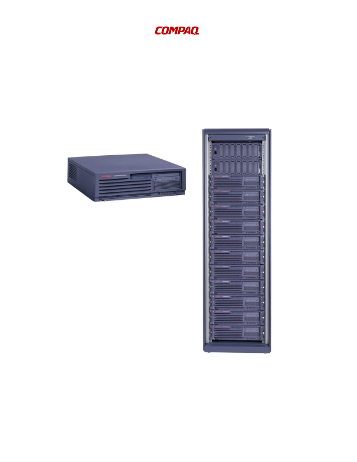
Compaq AlphaServer DS10 Systems
The Compaq AlphaServer DS10 system is an entry-level
system offering 64-bit computing with the Alpha processor.
This single processor system is ideal for ISP/Internet applications, telecom applications, software development, and
replicated site applications. The 3-U system box can be
mounted in a cabinet or used on a desktop.
Compaq AlphaServer products use the 64-bit Alpha RISC
architecture that supports multiple operating systems:
Tru64 UNIX, OpenVMS, and Linux.
For more information on Compaq AlphaServer DS10
systems, see
http://www.compaq.com/alphaserver
System Overview
The Compaq AlphaServer DS10 systems are available with the
600 MHz Alpha chip, the 21264A (marketed as 600 MHz but
it actually runs at 616 MHz). Memory begins at 256 Mbytes
and can be increased to 2 Gbytes. Second-level cache is 2
Mbytes. The switch-based system interconnect exploits the full
potential of the Alpha chip.
The system meas ures 17 x 19 x 5 inches (3U) a nd can be
placed on a desktop or rackmounted in a choice of three Mseries cabinets, along with additional disks. In the largest
cabinet (79 inches) up to 12 systems can be installed, or if
more storage is desi red, there can be up to 6 StorageWorks
shelves and up to 8 systems. A rackmount slide kit is included
with each system.
Six drive bays are available for storage devices. Each system
includes a CD-ROM and floppy; a 5.25-inch r emovable media
device can be added. With four 1-inch disks, t here can be 218
GB of storage in the syste m box.
There are four full-length PCI slots: three 64-bit slots and one
32-bit slot. Integr ated on the system board are two 10/100 Mbit
fast Ethernet controllers, an IDE controller, two serial ports,
one parallel port, remote management console, and keyboard
and mouse ports.
Systems can be purchased with the Tru64 UNIX or OpenVMS
operating systems insta lled. Or they can be purchased without
any operating system, allowing customers to inst all Linux.
Features and Benefits
• Performance
The Alpha chip, the world’s fastest microprocessor, is offered
with a switch-base d interconnect that supports one 600 MHz
processor and up to 2 Gbytes of memory. This switch-based
system provides a memory bandwidth of up to 1.3 Gbytes/sec
(peak) using a 128-bit memory bus running at 77 M Hz. The
peak I/O bandwidth is 250 Mbyes/sec.
• Multiple Operating Systems
No other server offers the flexibility of running so many
operating systems: Tru64 UNIX, OpenVMS, and L inux. It’s
ideal as a development tool as well as a Web server or file
server, or for remote applica tions or E-comme rce applications.
• Package and Price
All the features of AlphaServers are now available in a
package that goes anyw here at a price attractive to everyone.
Start with one and then add to your base as your needs
demand. Use the DS10 as a dedicated system or set up a
cluster.
• DS10 Workstations
The 600 MHz system is also offered as a workstation and is
called the AlphaStation DS10.

Third-Generation Alpha Chip
The third genera tion of the Alpha microprocessor, the Alpha
21264, is a superscalar, superpipeline d i mplementation of the
Alpha architecture. The first offering of this chip, which was
manufactured using the CMOS-6 process, was known as EV6
and now the EV67 (21264A) chip is available, which uses the
CMOS-7 process. Over 15.2 million transistors are on one die.
In our discussion here, t he Alpha 21264 designation applies to the
EV6 and the EV67 chips, unl ess we need to distinguish betw een
the two. Designed f or performance, the Alpha 21264 achie ves this
goal by carefully st udi ed and simulated ar chitectural and circuit
analysis. The 21264 memory system also enable s t he high performance levels. On-chip and off-chip caches provide for very low
latency data access, which allows for very high bandwidth data
access. The 21264A 2-Mbyte off-chip cache runs at 205 MHz.
Internal to each chip is a 64-Kbyte instruction cache (I-cache)
and a 64-Kbyte data cache (D-cache).
• I-cache. 64 Kbytes, two-way set -associative, vir tually
addressed cache with 64-byte blocks
• D-cache. 64 Kbytes, two-way set -associative, virtually
indexed, physically tagged, writeback cache with 64-byte
blocks
Chip Operation
Several key design choices were made i n the chip architect ure
to maximize performance: Four instructions are fetched each
cycle, and then how those instructions are handled boosts the
speed of execution. Register renaming assigns a unique storage
location with each write reference to a register, avoiding register
dependencies that can be a potential bottleneck to processor
performance.
Another design fea t ure, out-of-or der execution, permits
instructions to execute in an order different from the order that
the instructions are fetched. In effect, instructions execute as
soon as possible. This allows for faster e xe cution since critical
path computations ar e started and completed as soon as
possible.
In addition, the Alpha 21264 employs speculative execution to
maximize performance. It speculatively fetches and executes
instructions even though it may not know immediately whether
the instruction will be on the final execution path. This is
particularly use ful, for instance , when the 21264 predicts
branch directions and speculatively executes down the
predicted path. The sophisticated bra nch prediction in the
21264 coupled with the specul ative and dynamic e xecution
extracts the most instruction parallelism from applications.
For more inform ation about the chip, see
http://www.compaq.com/alphaserver/download/ev6chip.pdf
Alpha 21264 Features
• Out-of-order instruction execution
• Large (64 Kbyte) on-chip data and instruction caches
• Improved branch prediction through intuitive execution
• Register renaming
• Increased bandwidth for high-speed access to second-level
cache and system memory
• Motion video instructions
• Square root and divide instructions
• All instructions are 32 bits long and have a regular
instruction format
• Floating-point unit, supports DIGITAL and IEEE floating-
point data types
• 80 integer registers, 64 bits wide
• 72 floating-point re gisters, 64 bits wide
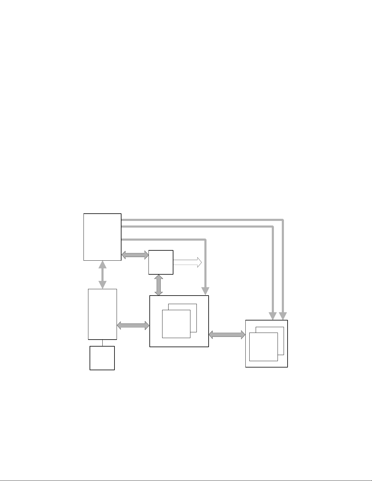
Architecture
The traditional bus interconnect has been replaced by a switchbased interconnect system. With a bus design, the processors,
memory, and I/ O modules share the bus. As the number of bus
users increases, the transactions interfere with one another,
increasing latency and decreasing aggregate bandwidt h.
However, with a switch-based system t here is no degradation
in performance as the number of CPUs, memory, and I/O users
increase. Although t he users increase, t he speed is maintained.
With a switch-based, or point-to-point interconnect, the
performance remains constant, even though the number of
transactions multiplies. The switched system inte rconnect uses
a set of complex chips that route the traffic over multiple paths.
The chipset consists of one C-chip, one P-chip, a nd t wo Dchips.
• C-chip. Provides the command interface from the CPU.
• D-chips. Provide the data path for the CPU, main
memory, and I/O.
• P-chip. Provides the interface to the PCI bus.
System Block Diagram
This chipset, similar to those used in the AlphaServer DS20
and ES40 systems, supports up to one CPU and up to 2 Gbytes
memory. Interleaving occurs when at least two memory arrays
are used.
The PAD bus, the interface between the P-chip and the Dchips, is 32 data bits with 4 check bits. The 128-bit memory
bus supports two memory arrays, yielding a 1.3 Gbyte/sec
system bandwidth. Tr ansactions are ECC prot ected. Upon the
receipt of data, the receiver checks for data integrity and
corrects any errors.
C-chip
CPU
B-cache
Command, Address, and Control lines for each Memory Array
Control lines for D-chips
CAP Bus
CPU
Data Bus
P-chip
64 bit PCI
PAD
Bus
2 D-chips
Memory
Data Bus
1 or 2
Memory
Arrays
PKW
1400B-99

System Board
The interconnect switch is implemented on the system board
by the chipset consisting of one C-chip, one P-chip, and two
D-chips. The chipset provides the data and address path
between the CPU, me mory, and the I/O subsystem.
The CPU installed on the system board is the Alpha 21264A
(600 MHz). The four cache chips provide 2 Mbytes of secondlevel cache. A flash ROM holds the SRM console code, the
AlphaBIOS console code, and the NVRAM da ta. The remote
management consol e (RMC) is imple mented by the RMC
processor and is accessed through the COM1 port. Integrated
Component and Connector Locations
CPU
COM1 and RMC
COM2
into the system board is the logic needed for all the ports
shown on the left side of the module, including the two
Ethernet ports, and also for the two IDE connectors.
Jumpers on the board al low you to change the acti on of the
Halt button and disable the RMC timer.
Connectors are on the syst em board for five ot her cards: the
PCI riser card and four memory DIMMs.
Memory
Keyboard, Mouse
Parallel Port
Ethernet
Ethernet
PCI Riser Card
D
Chip
P
Chip
RMC
Processor
C
Chip
D
Chip
Halt/Reset Jumper
RMC Jumper
IDE
PK0331-99

Memory
Memory throughput is maximized by the following featur es:
• 128-bit wide mem ory data bus
• Very low memory latency (120 ns) a nd hi gh bandwidth
with 12 ns clock
• ECC memory
The switch inter connect can move a l arge amount of data over
the memory data bus. The data bus is 128 bits wide (16 bytes).
With the memory bus speed of 77 MHz, the maximum
bandwidth is 1.3 GB/sec.
Memory Configuration
• Systems come with one memory option (two DI MMs)
installed in Bank 0.
• Both DIMMs in a bank must be the same type and size.
• A second set of DIM Ms can be added.
Memory Bank 0 Memory Bank 1
Address Arrays 0 & 1
128 Data + 16 Check Bits
Data
C-Chip
Bus
To Both D-Chips
PK0272A
Memory Options
Each memory opt i on consists of two 200-pin industry-standard
DIMMs. The DIMMs are synchronous DRAMs. Memory
options are available in the following sizes:
• 256 Mbytes (128 MB DIMMs)
• 512 Mbytes (256 MB DIMMs)
• 1 Gbyte (512 MB DIMMs)
The system supports 2 Gbytes of memory.
Bank 0
Bank 1
PK0331A-99
Memory Performance Considerations
With one memory opti on (2 DIMMs), memory operation
interleaving will not occur. With two memory options (4
DIMMs), memory read-write operations are two-way
interleaved. Interleaved operations reduce the average latency
and increase the memory throughput ove r noninterleaved
operations.

System I/O
The industry-standard PCI bus is the number one choice for
high-performa nce I/O options, such as disk storage and highperformance video applications.
The PCI bus implementation has the following characteristics:
• Fully compliant with the PCI Version 2.1 Specification
• Operates at 31 M Hz, delivering a peak bandwidth of 250
Mbytes/sec.
Block Diagram of I/O Control
• Supports three address spaces: PCI I/O, PCI mem or y, and
PCI configuration space
• Supports byte/word, tri-byte, and longword operations
• Exists in noncached address space only
P-chip
Flash ROM
(NVRAM functions)
C-chip
Interrupts
Config
The industry-standard PCI I/O bus allows you to use inexpensive,
widely available I/O options. Both 32-bit and 64-bit PCI options
can be used; 3.3V and 5V opt ions are supported.
The Acer Labs 1543C c hi p provides the bridge fr om the PCI
to lower level bus functions. The C-chip controls accesses to
memory on behalf of the P-chip. Two T ul ip chips provide
control for the two integrated Ethernet ports. On the PCI riser
card are four PCI slots; three 64-bit slots and one 32-bit slot,
which can be used for a video controller.
I/O Ports
At the rear of the system are connectors offering access to two
serial communi cation ports, one parallel port, tw o Ethernet
ports, and ports for the keyboard and mouse. (The USB ports
are not supported.) The COM1 port is used for t he system
console and for the r emote management console.
Tulip 21143
PCI Slots
PCI Slot 4
PCI Slot 3
PCI Slot 2
PCI Slot 1
Acer Labs
1543C Chip
COM1
COM2
Printer
Floppy
PCI Slot
Keyboard
Mouse
CD-ROM
Ethernet
PK-0319B-99
64 Bit
64 Bit
64 Bit
32 Bit
PK1045-99
1
3
5
6
2 4
1
2
B
A
PK0334A-99
1. COM1 and RMC port
2. COM2 port
3. Mouse
4. Keyboard
5. USB ports (not supported)
6. Parallel port
7. Ethernet A
8. Ethernet B
7 8

System Control
Close monitoring and control of the system environment and
hardware is done by the remote ma nagement console (RMC).
This logic allows the system operator to perform console
operations remotely using a dial-in mode m. The RMC logic is
implemented using a PIC17C44 microprocessor on the system
board. The RMC fir mware code resi des on the microproce ssor
and in flash memory. The RMC is powered by an auxiliary
5V supply, so even when the system is powered off a t the
control panel the RMC can be accessed—so long as the system
is plugged in.
The RMC provides the f ol lowing monitoring and control
functions:
• Monitors thermal sensors, the power supply, and fans
• Detects alert conditions such as excessive temperature, fan
failure, and power supply failure and sends an alert
• Performs remote power on/off, ha lt, and reset
• Dials a pager phone number or another c omputer system
to notify the remote operator of an alert condition
• Shuts down the system if any fatal conditions exist
Upon an environmental event, the reas on for failure is stored
in the RMC NVRAM; the data can be retrieved to aid in
diagnosing the problem.
Control Panel
The system control buttons and indicator LEDs are located in
the lower right corner on the front of the system.
1
1
3
2
2
Internal
Storage Cage
Configuration
1 Floppy disk drive 3 CD-ROM
2 Internal drive bay 4 Internal drive/tape bay
5 Internal drive bay
The front access storage cage systems have six storage/media
bays. In addition to the floppy and CD-ROM, the four other
storage bays can support two front access 3.5” x 1” hard disk
drives and two internal 3.5” x 1” hard disk drives or one front
access universal tape drive (AIT or DAT) and two internal
disk drives.
1
1
2
2
Front Access
Storage Cage
Configuration
3
4
4
5
5
MR0052A
3
3
4
4
5
5
6
6
PK1043BT
The operation of the button at the left depends upon the setting
of a jumper. It functions as a Hal t button with Tru64 UNIX
and OpenVMS.
Storage
The DS10 comes with either an internal storage cage or a front
access storage cage. The internal storage cage systems have
five storage/media bays. In addition t o t he floppy and CDROM, the other thr ee storage bays can support three internal
3.5” x 1” hard disk drives or two internal 3.5” x 1” hard disk
drives and one 5.25” x 1.6” removable media device.
Disks supported are 20 and 40 GB IDE disks and 18.2 and 36.4
GB UltraSCSI disks. In addition, a 72.8 GB unive rsal wide
Ultra3 SCSI disk is supported with the front access storage
cage.
MR0053A
1 Floppy disk drive 3 CD-ROM
2 Internal drive bay 4 Compaq universal drive bay
5 Compaq universal drive bay
6 Internal drive bay
RAID (Redundant Array of Independent Disks)
The system can be configured with optional PCI RAID
controllers to organize disk data cost- effectively, improve
performance, and provide high levels of storage integr ity.
Today, RAID is only ava ilable with StorageWorks shelves.
The optional RAID controllers have the following features:
• Support for hot-swap drives
• Automatic rebuild after hot swap
• Console support for booting system from RAID
• RAID levels 0, 1, 0+1, 5
• Optional write cache
• Optional read cache
• Support for command queuing

Server Management
The AlphaServer products support important operational and
platform management requirements.
Operational Management
Server/Network Management . Compaq Insight Manager is
included with every syst em. This software tool allows you to
monitor and control Alpha based servers. Insight Manager
consists of two component s: a Windows-based console appl i cation and server - or client-based management data collection
agents. Management agents monitor over 1,000 management
parameters. Key subsystems are inst rumented to make he alth,
configuration, and performance data available to the agent
software. The agents act upon that data, by initiating alarms in
the event of faul t s and by providing updated management information, such as network interface or storage subsystem performance statistics.
Remote Server Management. The integrated remote management console (RMC) lets the operator perform several tasks
from a serial console: monitor the system power, temperature,
and fans, and reset , halt, and power the system on or off. The
monitoring can be done locally or remotely through a modem.
Platform Management
The AlphaServer DS10 systems support platform ma nagement
tasks such as manipulat ing and monitoring hardware performance, configuration, and errors . For example, the operating
systems provide a numbe r of tools to characterize system per formance and displ ay errors logged in the syst em error log fi le.
In addition, system c onsol e firmware provides hardware
configuration tools and diagnostics to facilitate quick hardware
installation and troubleshooting. The system ope rator can use
simple console commands to show the system confi guration,
devices, boot and oper ational flags, and recorded errors. Also,
the console provides inventory support and configuration
management by giving access to serial numbers and revisions
of hardware and firmware.
Error Reporting
Compaq Analyze, a di agnostic service tool use d t o determine
the cause of hardware failures, is installed with the operating
systems. It provides automatic background a nalysis, as it
constantly views and re ads the error log fi l e. It analyzes both
single error/fault events and multiple events. When an error
condition is detected, it collects the error information and
sends it and an analysis to the user. The tool requires a
graphics monitor for its output display.
Security
• The top cover can be locked with a key.
• Password protection is offered by the SRM consol e and
RMC.
Reliability and Availability Features
The AlphaServer DS10 system a chieves an unparalleled level
of reliability and availability through the careful application of
technologies that ba l ance redundancy, e rror correction, and
fault management. Reliability and availability features are
built into the CPU, memory, and I/O, and implemented at the
system level.
Processor Features
• CPU data cache provides error correction code (ECC)
protection.
• Parity protection on CPU cache tag store.
• Multi-tiered power-up diagnostics to ve rify the
functionality of the hardware.
Memory Features
• The memory ECC sc heme is designed to provide maxi-
mum protection f or user data. The memory scheme
corrects single-bit errors and detects double-bit errors and
total DRAM failure.
I/O Features
• ECC protection on the switch interconnect and parity
protection on the PCI and SCSI buses.
• Extensive error correction built into disk drives.
• Optional internal RAID improves reliability and data
security.
System Features
Auto reboot. On systems runni ng Tru64 UNIX or OpenVMS, a
firmware environment varia ble lets you set the def ault action
the system takes on power-up, reset, or after an operat i ng
system crash. For maximum system availability, the variable
can be set to cause the syste m to automatically r eboot the
operating system after most syste m failures.
Software installation. The operating systems are factory
installed. Factor y i nst alled software (FIS) allows you to boot
and use your system in a short er time than if you install the
software from a distribution kit.
Diagnostics. During the power-up process, diagnostics are run
to achieve several goals:
• Provide a robust hardware platform for the operating
system by ensuring that any faulty hardware does not
participate in the operating system session. This maximizes system uptime by reducing the risk of system
failure.
• Enable efficient, timely repair.
Audible beep codes re port the status of diagnostic testing.
The system has a firmware update utility (LFU) that provides
update capability for console and PCI I/O adapter firmware. A
fail-safe loa der provides a means of reloading the console in
the event of corrupted firmware.
Thermal management. The air temperature and fan ope ration
are monitored to protect against overheating and possible
hardware destr uction. Four fans provide cooling. The system
fan is under the fl oppy drive; another fa n cools the PCI area.
Also, a fan is mounted over the Alpha chi p, and the power

supply has a fan. If the temperature rises, the system fa n
speeds up; or if necessary to prevent damage, the system shuts
down.
Error handling. Parity and othe r error conditions a re detected
on the PCI bus. The memory checking scheme corrects singlebit errors and det ects double-bit errors. Multiple ECC
corrections to single-bit errors de t ected by the operati ng
systems help in determining where in the system the error
originated. Errors are logged for analysis.
Uninterruptible power supply. An external UPS can be
purchased to support critical customer configurations. Because
power is maintained for the entire system (CPU, memory, and
I/O), power interruptions are completely transparent to users.
Clustering
A cluster is a loosely coupled set of systems that behaves (is
addressed and manage d) like a single system, but provides
high levels of availability through redundant CPUs, storage,
and data paths. Cluster s are also highly scalabl e; that is, CPU,
I/O, storage, and application resources can be added inc rementally to efficiently increase capacity. For customers, this
translates to reliable access to system resources and data, and
investment protection of both hardware and software.
Clustering allows multiple computer systems to communicate
over a common interface, share disks, and spread the computing load across multiple CPUs.
PCI to Memory Channel Interconnect
Under Tru64 UNIX a nd OpenVMS, you can build high-availability clusters using the PCI to Memory Cha nne l interconnect.
The Memory Channe l interconnect is a high-bandwidth, lowlatency PCI-base d communications inte rconnect for up to ei ght
AlphaServer systems. Data written to one computer’s memory
is shared by other computers on the
The PCI adapter is the interface between a PCI and a Memory
Channel bus. This bus is a m emory-to-memory computer
system interconnect that permits I/O space writes in one
computing node to be re plicated into the m emories of all ot her
nodes on the Memory Channe l bus. A write performed by any
CPU to its reflected address region results in automatic
hardware updates to memory regions in other nodes. One
node’s write is “reflected” to other nodes as a direct side effe ct
of the local wri t e. This provides a m emory region with
properties similar to a high-performance shared memory
across a group of nodes.
Operating System Support
For clustered Tru64 UNIX systems, TruCluster Software
solutions allow users access to network services and provide
further failover recovery from server, network, or I/O failures.
Tru64 UNIX cluster systems use the SCSI bus and/or PCI to
Memory Channel interconnect bus between disks a nd systems.
Memory Channel bus.
OpenVMS cluster systems use the CI, SCSI, Ethernet, FDDI,
and Memory Channel a s the interconnect be t ween disks and
the system.
The primary m eans of clustering AlphaServer DS10 systems
depends on the operating system.
• Ethernet, OpenVMS
• CI clusters, OpenVMS only
• Memory Channel, Tru64 UNIX and OpenVMS
• SCSI clusters, Tru64 UNIX and OpenVMS
Performance
Compaq has an ongoing program of performance engineering,
using industry-standard be nchmarks that allow comparisons
across major vendors’ systems. These benchmarks against
competitive systems are based on comparable CPU performance, coupled with comparable memory and disk expandability.
See Table 1 for the performance numbers of the AlphaServer
DS10 systems. System pe rformance, how ever, is highly dependent upon application c haracteristics. Thus, benchmark
information is one helpful “data point” to be used in conjunction with other purchase criteria such as features, service, and
price.
Sources of Performance Information
Performance information is available on the Internet.
http://www.compaq.com/alphaserver/performance/index.html
http://www.ideasinternational.com/benchmark/spec/specfp_s2000.html
Information for Partners
If you are a Channel or Reseller Partner, you can find the tools,
resources, and information you need to conduct business
online on the secure Compaq Business Partner site:
http://bps.compaq.com/businesspartner
Also see the following:
Compaq Solutions Alliance site at http://csa.compaq.com
and HP’s Developer and Solution Partner Portal (DSPP) ,
http://www.hp.com/go/partners

Service and Support
Compaq provides a compr ehensive set of services that
range from m igration, consulting, and training, to direct
support of Alpha systems, software, and appli cations. For
information on services, see
http://www.compaq.com/services
http://www.hp.com/hps/
Hardware Warranty
The AlphaServer DS10 system and components, including
CPU, memory, PCI controllers, and power supplies, have a
3-year on-site, 5-day per week, 9-hour per day hardware
warranty with next business day response time .
StorageWorks component s are supported by the com prehensive StorageWorks war ranty: five years for disks, three year s
for controllers, two years for tape devices, and one year for
other components. T he first year inc ludes on-site next-day
response time. N etwork products carry the network products
warranty.
Users can upgrade t o higher levels of service through a variety
of hardware supple mental services.
Software Warranty
The warranty for Tru64 UNIX and OpenVMS is conformance
to SPD with advisory tele phone support for a period of 90
days. Users can upgrade to higher levels of service through a
variety of softwa re supplemental services.

Compaq AlphaServer DS10 System Diagrams
3
2
1
4
5
6
7
8
9
FRONT
4
5
6
9
8
I/O PORTS
1. PCI riser card
2. CPU and fan
3. Power supply
4. CD-ROM
5. Optional bay
6. System disk
7. Control panel
8. Floppy diskette drive
9. Concealed optional bay
10. Memory
1
2
A
B
PK0334-99
3
2
REAR
1
3
5
2 4
1. COM1 and RMC port
2. COM2 port
3. Mouse
4. Keyboard
1
7 8
6
5. USB ports (not supported)
6. Parallel port
7. Ethernet A
8. Ethernet B
10
PK0332B

System Features at a Glance
Table 1 provides a quick reference to features of t he Compaq AlphaServer DS10 systems.
Table 1 AlphaServer DS10 Features
CPU Features 67/600
Processor One Alpha 21264A
CPU clock speed 600 MHz (actually 616 MHz)
Cache on chip
On-board cache 2 MB
Memory (maximum)
Performance 67/600
SPECint2000 364
SPECfp2000 411
SPECint95 35.3
SPECfp95 56.1
SPECint_rate95 319
SPECfp_rate95 505
Linpack 100x100 483.4
Linpack (1kx1k) 900.9
Standard Features
Internal Storage
Removable media CD-ROM, floppy diskette , optional tape drive
System storage 108 GB SCSI or 120 GB IDE with internal storage cage or 218 GB SCSI with front access st orage cage
I/O System
I/O slots 3 64-bit PCI slots and 1 32-bit PCI slot
Maximum PCI throughput 250 MB/sec
High Availability Features
System Auto reboot, thermal management, remote management consol e, RAID, ECC memory, ECC cache,
OpenVMS clusters Ethernet, DSSI, SCSI, FDDI, PCI to Memory Channel Interconnect
UNIX TruCluster Solutions SCSI, PCI to Memory Channel Interconnect
Operating Systems
Warranty
Hardware 3-year, on-site, 5 day x 9 hour warranty with next business day response
Software
64 KB I-cache
64 KB D-cache
2 GB
1.44 MB diskette drive, CD-ROM drive, 10/100 Mbit Ethernet ports, IDE controller, 2 serial ports, 1
parallel port, keyboard and mouse, integrated remote management console, rackmount slide kit,
operating system license and customer documentation, Internet software
error logging, optional uninterruptible power supply. Also with rackmount: multiple systems, multiple
power sources, dual-ported storage
Tru64 UNIX, OpenVMS, and Linux
90-day telephone advisory support for OpenVMS and T r u64 UNIX

Physical Characteristics
Table 2 details basic physical characteristics of the system.
Table 2 AlphaServer DS10 Physical Characteristics
Dimensions
Height 13.0 cm (5.1 in.)
Width 44.6 cm (17.6 in.)
Depth 48.4 cm (19.1 in.)
Weight 14.5 kg (32 lb) typical;
16.3 kg (36 lb) maximum
Environmental
Temperature
Humidity (noncondensing) Operating
Maximum altitude (unpressurized) Operating
Nonoperating shock 30 G, 25 ms halfsine
Electrical
Nominal voltage range (Vac)
Operating voltage range (Vac)
Power source phase
Nominal frequency (Hz)
Frequency range (Hz)
Maximum inrush current (amps)
Single power supply (amps)
Acoustics—Declared values per ISO 9296 and ISO 7779
Current values for specific configurations are available from Compaq. 1 B = 10 dBA
DS10 with 1 HDD
Idle
Operating
Operating
Nonoperating
10–40° C (50–104° F)
–40 to 66° C (–40 to 151° F)
20–80%
Nonoperating
10–95%
3037 m (10,000 ft)
Nonoperating
100–120/220–240
12,192 m (40,000 ft)
90–128/180–265
Single/Single
60/50
59–61/49–51
11/22
12/5
L
Wad
5.7
6.0
, B
, dBA
L
pAm
(operator position)
48
52
, dBA
L
pAm
(bystander positions)
41
45

© 2002 Compaq Computer Corporation
Compaq, the Compaq logo, Compaq Insight Manager, AlphaServer,
StorageWorks, and TruCluster Registered in U.S. Patent and Trademark
Office. OpenVMS and Tru64 are trademarks of Compaq Information
Technologies Group, L.P. in the United States and other countries.
Linux is a registered trademark of Linus Torvalds in several countries.
SPECint95, SPECfp95, SPECint2000, SPECfp2000, and SPECweb96 are
registered trademarks of the Standard Performance Evaluation Corporation.
UNIX is a trademark of The Open Group in the United States and other
countries. All other product names mentioned herein may be trademarks of
their respective companies.
Compaq shall not be liable for technical or editorial errors or omissions
contained herein. The information in this document is provided “as is”
without warranty of any kind and is subject to change without notice. The
warranties for Compaq products are set forth in the express limited warranty
statements accompanying such products. Nothing herein should be
construed as constituting an additional warranty.
 Loading...