

Page 1
Technical
Reference
Guide
For the
Compaq Deskpro EN Series of Personal Computers
Desktop and Minitower Form Factors
Page 2

This hardcopy is designed to be placed into a standard 3-ring binder. Provided below is a title block that
can be copied and cut out and placed into the slip or taped onto the edge of the binder.
Deskpro EN Series of Personal Computers
Desktop and Minitower Form Factors
TRG
Page 3

Reader Feedback
Please feel free to send any questions, suggestions, corrections, or comments regarding this
document please to the following email address:
Desktop.training.feedback@Compaq.com
When responding, please state the title of the referenced document.
Page 4

Technical Reference Guide
NOTICE
The information in this document is subject to change without notice.
COMPAQ COMPUTER CORPORATION SHALL NOT BE LIABLE FOR TECHNICAL OR
EDITORIAL ERRORS OR OMISSIONS HEREIN; NOR FOR INCIDENTAL OR
CONSEQUENTIAL DAMAGES RESULTING FROM THE FURNISHING, PERFORMANCE,
OR USE OF THIS MATERIAL. IT IS THE RESPONSIBILITY OF MANUFACTURERS TO
ENSURE THAT DEVICES DESIGNED TO BE USED WITH COMPAQ PRODUCTS
COMPLY WITH FCC CLASS B EMISSIONS REQUIREMENTS.
This guide contains information protected by copyright. No part of this document may be
photocopied or reproduced in any form without prior written consent from Compaq Computer
Corporation.
1998 Compaq Co mputer Cor poration
All rights reserved. Printed in the US A
Compaq, Deskpro, LTE, Contura, Presario, ProLinea
Registered U.S. Patent and Trademark Office
Product names mentioned in this document may be trademarks and/or registered trademarks of other companies.
“Pentium” and “MMX ” are trad emarks of Intel Corporation.
“Windows” is a trademark of Microsoft Corporation.
For more information regarding specifications and Compaq-specific parts please contact Compaq
Computer Corporation.
Technical Reference Guide
Compaq Deskpro EN Series of Personal Computers, Desktop and Minitower Form Factors
Third Edition - Se ptember 1998
Documen t Number DSK-113C /0498
for
Compaq Deskpro EN Series of Personal Computers
Desktop and Minitower Form Factors
Third Edi tion - September 1998
i
Page 5

Technical Reference Guide
ii
Compaq Deskpro EN Series of Personal Computers
Desktop and Minitower Form Factors
Third Edi tion–- September1998
Page 6

Technical Reference Guide
TABLE OF CONTENTS
CHAPTER 1 INTRODUCTION.............................................................................................................
1.1 ABOUT THIS GUIDE...........................................................................................................1-1
1.1.1 USING THIS GUIDE.....................................................................................................1-1
1.1.2 ADDITIONAL INFORMATION SOURCES.................................................................. 1-1
1.2 NOT ATIONAL CONVENTIONS .......................................................................................... 1-2
1.2.1 VALUES........................................................................................................................ 1-2
1.2.2 RANGES........................................................................................................................ 1-2
1.2.3 SIGNAL LABELS.......................................................................................................... 1-2
1.2.4 REGISTER NOTATION AND USAGE .........................................................................1-2
1.2.5 BIT NOTATION............................................................................................................1-2
1.3 C OMMON ACRONYMS AND ABBREVIATIONS..............................................................1-3
CHAPTER 2 SYSTE M OVERVIEW .....................................................................................................
2.1 INTRODUCTION..................................................................................................................2-1
2.2 FE ATURES AND OPTIONS................................................................................................. 2-2
2.2.1 STANDARD FEATURES..............................................................................................2-2
2.2.2 OPTIONS.......................................................................................................................2-3
2.3 MECHANICAL DESIGN......................................................................................................2-4
2.3.1 CABINET LAYOUTS.................................................................................................... 2-4
2.3.2 CHASSIS LAYOUTS..................................................................................................... 2-6
2.3.3 BOARD LAYOUTS....................................................................................................... 2-8
2.4 SYSTEM ARCHITECTURE................................................................................................2-10
2.4.1 PROCESSOR...............................................................................................................2-12
2.4.2 SYSTEM MEMORY....................................................................................................2-13
2.4.3 SUPPORT CHIPSET.................................................................................................... 2-13
2.4.4 MASS STORAGE........................................................................................................ 2-13
2.4.5 SERIAL AND PARALLEL INTERFACES .................................................................. 2-14
2.4.6 UNIVERSAL SERIAL BUS INTERFACE................................................................... 2-14
2.4.7 GRAPHICS SUBSYSTEM........................................................................................... 2-14
2.4.8 AUDIO SUBSYSTEM.................................................................................................2-14
2.5 SPECIFICATIONS..............................................................................................................2-15
CHAPTER 3 PROCESSOR/MEMORY SUBSYSTEM........................................................................
3.1 INTRODUCTION..................................................................................................................3-1
3.2 PROCE SSOR/ME MORY SUBSYSTEM .............................................................................. 3-2
3.2.1 PROCESSOR.................................................................................................................3-3
3.2.2 PROCESSOR CHANGING/UPGRADING..................................................................... 3-5
3.2.3 SYSTEM MEMORY......................................................................................................3-6
3.2.4 SUBSYSTEM CONFIGURATION.................................................................................3-9
Compaq Deskpro EN Series of Personal Computers
Desktop and Minitower Form Factors
Third Edi tion - September 1998
iii
Page 7

Technical Reference Guide
CHAPTER 4 SYSTEM SUPPORT.........................................................................................................
4.1 INTRODUCTION..................................................................................................................4-1
4.2 PCI BUS OVERVIEW........................................................................................................... 4-2
4.2.1 PCI CONNECTOR ......................................................................................................... 4-3
4.2.2 PCI BUS MASTER ARBITRATION..............................................................................4-4
4.2.3 PCI BUS TRANSACTIONS...........................................................................................4-5
4.2.4 OPTION ROM MAPPING ............................................................................................. 4-8
4.2.5 PCI INTERRUPT MAPPING.........................................................................................4-9
4.2.6 PCI POWER MANAGEMENT SUPPORT.....................................................................4-9
4.2.7 PCI CONFIGURATION............................................................................................... 4-10
4.3 AGP BUS OVERVIEW ....................................................................................................... 4-11
4.3.1 BUS TRANSACTIONS................................................................................................ 4-11
4.3.2 AGP CONFIGURATION.............................................................................................4-14
4.3.3 AGP CONNECTOR.....................................................................................................4-15
4.4 ISA BUS OVERVIEW.........................................................................................................4-16
4.4.1 ISA CONNECTOR ...................................................................................................... 4-17
4.4.2 ISA BUS TRANSACTIONS......................................................................................... 4-18
4.4.3 DIRECT MEMORY ACCESS......................................................................................4-20
4.4.4 INTERRUPTS.............................................................................................................. 4-23
4.4.5 INTERVAL TIMER..................................................................................................... 4-27
4.4.6 ISA CONFIGURATION............................................................................................... 4-27
4.5 SYSTEM CLOCK DISTRIBUTION....................................................................................4-28
4.6 REAL-T I ME C LOCK AND C ONFIGURATION MEMORY............................................... 4-29
4.7 I / O MAP AND REGI ST E R ACCESSING............................................................................ 4-46
4.7.1 SYSTEM I/O MAP ...................................................................................................... 4-46
4.7.2 GPIO UTILIZATION................................................................................................... 4-47
4.8 SYST EM MANAGEMENT SUPPORT ............................................................................... 4-51
4.8.1 FLASH ROM WRITE PROTECT ................................................................................ 4-52
4.8.2 PASSWORD PROTECTION........................................................................................ 4-52
4.8.3 I/O SECURITY............................................................................................................ 4-53
4.8.4 USER SECURITY........................................................................................................ 4-53
4.8.5 TEMPERATURE SENSING........................................................................................4-54
4.8.6 SMART COVER LOCK............................................................................................... 4-55
4.8.7 SMART COVER REMOVAL SENSOR ....................................................................... 4-55
4.8.8 POWER MANAGEMENT ........................................................................................... 4-56
CHAPTER 5 INPUT/OUTPUT INTERFACES.....................................................................................
5.1 INTRODUCTION..................................................................................................................5-1
5.2 ENHANCED IDE INTERFACE............................................................................................5-1
5.2.1 IDE PROGRAMMING................................................................................................... 5-1
5.2.2 IDE CONNECT OR ........................................................................................................ 5-8
5.3 DISKETTE DRIVE INTERFACE..........................................................................................5-9
5.3.1 DISKETTE DRIVE PROGRAMMING ........................................................................ 5-10
5.3.2 DISKETTE DRIVE CONNECTOR.............................................................................. 5-13
5.4 SERIAL INTERFACES.......................................................................................................5-14
5.4.1 RS-232 INTERFACE ................................................................................................... 5-14
5.4.2 SERIAL INTERFACE PROGRAMMING.................................................................... 5-15
iv
Compaq Deskpro EN Series of Personal Computers
Desktop and Minitower Form Factors
Third Edi tion–- September1998
Page 8

Technical Reference Guide
5.5 PARALLEL INTERFACE................................................................................................... 5-20
5.5.1 STANDARD PARALLEL PORT MODE.....................................................................5-20
5.5.2 ENHANCED PARALLEL PORT MODE..................................................................... 5-21
5.5.3 EXTENDED C APABILIT IES PORT MODE...............................................................5-21
5.5.4 PARALLEL INTERFACE PROGRAMMING.............................................................. 5-22
5.5.5 PARALLEL INTERFACE CONNECT OR ................................................................... 5-26
5.6 KEYBOARD/POINTING DEVICE INTERFACE ............................................................... 5-27
5.6.1 KEYBOARD INTERFACE OPERATION ................................................................... 5-27
5.6.2 POINTING DEVICE INTERFACE OPERATION ....................................................... 5-29
5.6.3 KEYBOARD/POINTING DEVICE INTERFACE PROGRAMMING ......................... 5-29
5.6.4 KEYBOARD/POINTING DEVICE INTERFACE CONNE C T OR................................ 5-33
5.7 UNIVERSAL SERIAL BUS INTERFACE...........................................................................5-34
5.7.1 USB KEYBOARD CONSIDERATIONS...................................................................... 5-34
5.7.2 USB CONFIGURATION..............................................................................................5-34
5.7.3 USB CONTROL........................................................................................................... 5-35
5.7.4 USB CONNECTOR ..................................................................................................... 5-35
CHAPTER 6 AUDIO SUBSYSTEM ......................................................................................................
6.1 INTRODUCTION..................................................................................................................6-1
6.2 FUNCTI ONAL DESC RIPT ION............................................................................................. 6-2
6.2.1 PCM AUDIO PROCESSING..........................................................................................6-4
6.2.2 FM SYNTHESIS AUDIO PROCESSING....................................................................... 6-7
6.3 PROGRAMMING.................................................................................................................. 6-8
6.3.1 CONFIGURATION........................................................................................................ 6-8
6.3.2 CONTROL..................................................................................................................... 6-9
6.4 SPECIFICATIONS .............................................................................................................. 6-11
CHAPTER 7 POWER SUPPLY AND DIST RIBUTION.......................................................................
7.1 INTRODUCTION..................................................................................................................7-1
7.2 POWE R SUPPLY ASSEMBLY/CONTROL ..........................................................................7-1
7.2.1 POWER SUPPLY ASSE MB L Y.....................................................................................7-2
7.2.2 POWER CONTROL....................................................................................................... 7-3
7.3 POWER DISTRIBUTION......................................................................................................7-5
7.3.1 3.5/5/12 VDC DISTRIBUTION......................................................................................7-5
7.3.2 LOW VOLTAGE DISTRIBUTION................................................................................ 7-6
7.4 SI GNAL DIST RIBUTION.....................................................................................................7-7
CHAPTER 8 BIOS ROM .......................................................................................................................
8.1 INTRODUCTION..................................................................................................................8-1
8.2 BOOT/RESET FUNCTIONS................................................................................................. 8-2
8.2.1 BOOT BLOCK...............................................................................................................8-2
8.2.2 QUICKBOOT.................................................................................................................8-2
8.2.3 SILENTBOOT ............................................................................................................... 8-2
8.2.4 RESET...........................................................................................................................8-2
Compaq Deskpro EN Series of Personal Computers
Desktop and Minitower Form Factors
Third Edi tion - September 1998
v
Page 9

Technical Reference Guide
8.3 MEMORY DETECTION AND CONFIGURATION.............................................................. 8-3
8.4 DE SKTOP MANAGEMENT SUPPORT ............................................................................... 8-4
8.4.1 SYSTEM ID...................................................................................................................8-6
8.4.2 SYSTEM INFORMATION TABLE ............................................................................... 8-6
8.4.3 EDID RETRIEVE........................................................................................................8-13
8.4.4 DRIVE FAULT PREDICTION.....................................................................................8-13
8.4.5 SYSTEM MAP RETRIEVAL....................................................................................... 8-14
8.4.6 FLASH ROM FUNCTIONS......................................................................................... 8-15
8.4.7 POWER BUTTON FUNCTIONS................................................................................. 8-15
8.4.8 ACCESSING CMOS.................................................................................................... 8-16
8.4.9 ACCESSING CMOS FEATURE BITS......................................................................... 8-16
8.4.10 SECURITY FUNCTIONS............................................................................................ 8-18
8.5 PNP SUPPORT.................................................................................................................... 8-19
8.5.1 SMBIOS....................................................................................................................... 8-20
8.6 POWE R MANAGEME NT FUNCTI ONS ............................................................................ 8-21
8.6.1 INDEPENDENT PM SUPPORT .................................................................................. 8-21
8.6.2 ACPI SUPPORT........................................................................................................... 8-21
8.6.3 APM SUPPORT........................................................................................................... 8-22
8.7 USB LEGACY SUPPORT ................................................................................................... 8-24
8.8 BIOS UPGRADING............................................................................................................. 8-24
APPENDIX A ERROR MESSAGES AND CODES...............................................................................
A.1 INTRODUCTION.................................................................................................................A-1
A.2 POWER-ON MESSAGES..................................................................................................... A-1
A.3 BEEP/KEYBOARD LED CODES........................................................................................ A-1
A.4 POWER-ON SELF TEST (POST) MESSAGES.................................................................... A-2
A.5 PROCESSOR ERROR MESSAGES (1
A.6 MEMORY ERROR MESSAGES (2
XX-XX
A.7 KEYBOARD ERROR MESSAGES (30
A.8 PRINTER ERROR MESSAGES (4
XX-XX
A.9 VIDEO (GRAPHICS) ERROR MESSAGES (5
A.10 DISKETTE DRIVE ERROR MESSAGES (6
A.11 SERIAL INTERFACE ERROR MESSAGES (11
A.12 MODEM COMMUNICATIONS ERROR MESSAGES (12
A.13 HARD DRIVE ERROR MESSAGES (17
A.14 HARD DRIVE ERROR MESSAGES (19
A.15 VIDEO (GRAPHICS) ERROR MESSAGES (24
A.16 AUDIO ERROR MESSAGES (3206A.17 NETWORK INTERFACE E RROR MESSAGES (60
A.18 SCSI INTERFACE E RROR MESSAGES (65
A.19 POINTING DEVICE INTERFACE ERROR MESSAGES (8601-
) ...................................................................... A-3
XX-XX
)........................................................................... A-4
)....................................................................... A-4
X-XX
)............................................................................ A-5
).......................................................... A-5
XX-XX
) ......................................................... A-6
XX-XX
)................................................... A-6
XX-XX
).................................... A-7
XX-XX
)............................................................... A-8
XX-XX
)............................................................... A-9
XX-XX
) .................................................... A-9
XX-XX
)......................................................................... A-10
XX
) ........................................... A-10
XX-XX
, 66XX-XX, 67XX-XX) ....................... A-11
XX-XX
).............................. A-11
XX
A.20 CEMM PRIVILEDGED OPS ERROR MESSAGES........................................................ A-12
A.21 CEMM EXCEPT I ON E RROR MESSAGES ................................................................... A-12
APPENDIX B ASCII CHARACTER SET .............................................................................................
B.1 INTRODUCTION..................................................................................................................B-1
vi
Compaq Deskpro EN Series of Personal Computers
Desktop and Minitower Form Factors
Third Edi tion–- September1998
Page 10

Technical Reference Guide
APPENDIX C KEYB O ARD ...................................................................................................................
C.1 INTRODUCTION..................................................................................................................C-1
C.2 KEYSTROKE PROCESSING................................................................................................C-2
C.2.1 TRANSMISSIONS TO THE SYSTEM ..........................................................................C-3
C.2.2 KEYBOARD LAYOUTS...............................................................................................C-4
C.2.3 KEYS .............................................................................................................................C-6
C.2.4 KEYBOARD COMMANDS...........................................................................................C-9
C.2.5 SCAN CODES...............................................................................................................C-9
APPENDIX D COMPAQ 10/100 TX PCI INTEL WOL UTP CONTROLLER CARD.......................
D.1 INTRODUCTION.................................................................................................................D-1
D.2 FUNCTIONAL DESCRIPTION............................................................................................ D-2
D.2.1 STATUS INDICATORS................................................................................................D-2
D.2.2 CARD POWER AND CLOCK...................................................................................... D-3
D.2.3 82558 CONTROLLER.................................................................................................. D-3
D.2.4 POWER MANAGEMENT SUPPORT........................................................................... D-4
D.3 CONFIGURATION/CONTROL ........................................................................................... D-5
D.4 RJ-45 CONNECTOR............................................................................................................ D-5
D.5 SPECIFICATIONS ...............................................................................................................D-5
APPENDIX E WIDE ULTRA SCSI HOST ADAPTE R ........................................................................
E.1 INTRODUCTION..................................................................................................................E-1
E.2 FUNCTIONAL DESCRIPTION.............................................................................................E-2
E.3 SCSI ADAPTER PROGRAMMING...................................................................................... E-3
E.3.1 SCSI ADAPTER CONFIGURATION ............................................................................ E-3
E.3.2 SCSI ADAPTER CONTROL .........................................................................................E-3
E.4 SPECIFCATIONS.................................................................................................................E-3
E.5 USER GUIDELINES.............................................................................................................E-4
E.6 SCSI
CONNECTORS ............................................................................................................E-5
APPENDIX F ATI RAGE PRO AGP 1X/2X GRAPHICS CARDS.......................................................
F.1 INTRODUCTION.................................................................................................................. F-1
F.2 FUNCTIONAL DESCRIPTION.............................................................................................F-2
F.2.1 ATI RAGE PRO TURBO AGP GRAPHICS CONTROLLER.........................................F-3
F.3 DISPLAY MODES................................................................................................................F-4
F.4 PROGRAMMING..................................................................................................................F-5
F.4.1 CONFIGURATION........................................................................................................F-5
F.4.2 CONTROL.....................................................................................................................F-5
F.5 MONITOR POWER MANAGEMENT CONT ROL ...............................................................F-6
F.6 CONNECTORS.....................................................................................................................F-6
F.6.1 MEMORY EXPANSI ON CONNECTOR.......................................................................F-6
F.6.2 MONIT OR CONNEC T OR............................................................................................. F-7
F.6.3 ATI MULTIMEDI A C HANNEL CONNEC T OR............................................................F-8
Compaq Deskpro EN Series of Personal Computers
Desktop and Minitower Form Factors
Third Edi tion - September 1998
vii
Page 11

Technical Reference Guide
LIST OF FIGURES
F
IGURE
F
IGURE
F
IGURE
F
IGURE
F
IGURE
F
IGURE
F
IGURE
F
IGURE
F
IGURE
F
IGURE
F
IGURE
F
IGURE
F
IGURE
F
IGURE
F
IGURE
F
IGURE
F
IGURE
F
IGURE
F
IGURE
F
IGURE
F
IGURE
F
IGURE
F
IGURE
F
IGURE
2–1. C
2–2. C
2–3. C
2–4. D
2–5. M
2–6. S
2–7. B
2–8. S
2–9. P
3–1. P
3–2. P
3–3. C
3–4. S
4–1. PCI B
4–2. PCI B
4–3. T
4–4. PCI C
OMPAQ DESKPRO
ABINET LAYOUTS
ABINET LAYOUTS
ESKTOP CHASSIS LAYOUT
INITOWER CHASSIS LAYOUT
YSTEM BOARD CONNECTOR AND SWITCH LOCATIONS
ACKLPANE BOARD CONNECTOR
YSTEM ARCHITECTURE
ROCESSOR PACKAGE COMPARISON
ROCESSOR/MEMORY SUBSYSTEM ARCHITECTURE
ENTIUM
ELERON PROCESSOR INTERNAL ARCHITECTURE
YSTEM MEMORY MAP
US DEVICES AND FUNCTIONS
US CONNECTOR
0 C
YPE
ONFIGURATION SPACE MAP
4–5. AGP 1X D
4–6. AGP 2X D
4–7. AGP B
4–8. ISA B
4–9. ISA E
4–10. M
4–11. C
US CONNECTOR
US BLOCK DIAGRAM
XPANSION CONNECTOR
ASKABLE INTERRUPT PROCESSING
ONFIGURATION MEMORY MAP
EN P
ERSONAL COMP UTER WITH MONITOR
, F
RONT VIEW
, R
EAR VIEW
, B
......................................................................................2-4
........................................................................................2-5
, T
OP VIEW
, L
LOCK DIAGRAM
..............................................................................2-6
EFT SIDE VIEW
, H
EADER, AND SWITCH LOCATIONS
...................................................................... 2-11
................................................................................ 2-12
II P
ROCESSOR INTERNAL ARCHITECTURE
.....................................................................................................3-8
....................................................................................4-2
(32-B
IT TYPE
ONFIGURATION CYCLE
).................................................................................4-3
........................................................................................4-6
......................................................................................4-7
ATA TRANSFER (PEAK TRANSFER RATE
ATA TRANSFER (PEAK TRANSFER RATE
...................................................................................................4-15
.............................................................................................4-16
..........................................................................................4-17
, B
LOCK DIAGRAM
.................................................................................... 4-29
...........................................2-1
................................................................2-7
......................................................2-8
................................2-9
............................................................3-2
............................................................3-3
...............................................................3-4
: 266 MB/S)........................................4-12
: 532 MB/S)........................................4-13
.................................................. 4-23
F
F
F
F
F
F
F
F
F
F
F
F
F
F
F
F
F
F
F
viii
5–1. 40-P
IGURE
5–2. 34-P
IGURE
5–3. S
IGURE
5–4. S
IGURE
5–5. P
IGURE
5–6. 8042-TO-K
IGURE
5–7. K
IGURE
5–8. U
IGURE
6–1. A
IGURE
6–2. A
IGURE
6–3. DAC O
IGURE
6–4. A
IGURE
6–5. FM S
IGURE
6–6. A
IGURE
7–1. P
IGURE
7–2. P
IGURE
7–3. L
IGURE
7–4. S
IGURE
7–5. B
IGURE
IDE C
IN
IN DISKETTE DRIVE CONNECTOR
ERIAL INTERFACES BLOCK DIAGRAM
ERIAL INTERFACE CONNECTOR (MALE
ARALLEL INTERFACE CONNECTOR (FEMALE
EYBOARD OR POINTING DEVICE INTERFACE CONNECTOR
NIVERSAL SERIAL BUS CONNECTOR (ONE OF TWO AS VIEWED FROM REAR OF CHASSIS
UDIO SUBSYSTEM BLOCK DIAGRAM
NALOG SIGNAL SAMPLING/QUANTIZING
UDIO SUBSYSTEM-TO
YNTHESIS PATCH
UDIO CAR-TO
OWER DISTRIBUTION AND CONTROL
OWER CABLE DIAGRAM
OW VOLTAGE SUPPLY
IGNAL DISTRIBUTION DIAGRAM
ACKPLANE HEADER PINOUTS
ONNECTOR
EYBOARD TRANSMISS I ON OF CODE EDH
PERATION
-ISA B
. ................................................................................................. 5-8
.............................................................................................................6-5
-ISA B
US
PCM A
......................................................................................................6-7
FM A
US
UDIO DATA FORMAT
..................................................................................................7-5
, B
LOCK DIAGRAM
.......................................................................................7-7
...........................................................................................7-8
Compaq Deskpro EN Series of Personal Computers
Desktop and Minitower Form Factors
.............................................................................. 5-13
............................................................................. 5-14
DB-9
AS VIEWED FROM REAR OF CHASSIS
DB-25
AS VIEWED FROM REAR OF CHASSIS
, T
IMING DIAGRAM
............................ 5-27
)...........5-14
).. 5-26
............................................... 5-33
).....5-35
................................................................................6-3
..........................................................................6-4
UDIO DATA FORMATS
/ B
YTE ORDERING
..............6-6
..........................................................6-7
, B
LOCK DIAGRAM
....................................................7-1
.........................................................................7-6
Third Edi tion–- September1998
Page 12

Technical Reference Guide
F
IGURE
F
IGURE
F
IGURE
F
IGURE
F
IGURE
F
IGURE
F
IGURE
F
IGURE
F
IGURE
F
IGURE
F
IGURE
F
IGURE
F
IGURE
F
IGURE
F
IGURE
F
IGURE
F
IGURE
F
IGURE
F
IGURE
C–1. K
C–2. K
C–3. U.S. E
C–4. N
C–5. U.S. E
C–6. N
D–1. C
D–2. C
D–3. 82558 C
D–4. E
E–1. W
E–2. A
E–3. U
E–4. W
EYSTROKE PROCESSING ELEMENTS
EYBOARD-TO-SYSTEM TRANSMISS I ON OF CODE 58H
NGLISH
ATIONAL
NGLISH WINDOWS
ATIONAL WINDOWS
OMPAQ
OMPAQ
THERNET
IDE ULTRA
DAPTEC
SCSI C
LTRA
IDE ULTRA
(101-KEY) K
(102-KEY) K
(102W-KEY) K
10/100 TX WOL C
10/100 TX PCI I
ONTROLLER INTERNAL ARCHITECTURE
TPE C
ONNECTOR
SCSI H
OST ADAPTER CARD LAYOUT
AHA-2940U U
ONNECTOR
SCSI C
ONNECTOR
F–1. ATI RAGE PRO AGP G
F–2. ATI RAGE PRO AGP G
F–3. ATI 3DR
F–4. VGA M
F–5. AMC C
AGE PRO GRAPHICS CONTROLLER INTERNAL ARCHITECTURE
ONITOR CONNECTOR
ONNECTOR
(40-P
, B
LOCK DIAGRAM
EYBOARD KEY POSITIONS
EYBOARD KEY POSITIONS
(101W-KEY) K
ONTROLLER CARD LAYOUT
WOL UTP C
NTEL
EYBOARD KEY POSITIONS
EYBOARD KEY POSITIONS
............................................................C-4
ONTROLLER CARD BLOCK DIAGRAM
............................................................... D-3
(RJ-45,
VIEWED FROM CARD EDGE
...........................................................E-1
SCSI A
LTRA
(50-
PIN, AS SEEN FROM REAR OF CARD
RAPHICS CARD LAYOUT
RAPHICS CARD BLOCK DIAGRAM
, (F
EMALE
IN HEADER
DAPTER CARD BLOCK DIAGRAM
(68-
PIN, AS SEEN FROM TOP OF CARD
(NLX
DB-15,
AS VIEWED FROM REAR
P1)...........................................................................F-8
....................................................C-2
, T
IMING DIAGRAM
..........................C-3
.......................................................C-4
...................................C-5
........................................C-5
(PCA# 323550-001)................. D-1
........... D-2
) ..................................... D-5
.............................E-2
)........................................E-5
).................................E-6
VERSION SHOWN
)...........................F-1
.................................................F-2
...............................F-3
)..............................F-7
Compaq Deskpro EN Series of Personal Computers
Desktop and Minitower Form Factors
Third Edi tion - September 1998
ix
Page 13

Technical Reference Guide
T
1–1. A
ABLE
CRONYMS AND ABBREVIATIONS
LIST OF TABLES
.......................................................................................1-3
2–1. M
T
ABLE
2–2. S
T
ABLE
2–3. G
T
ABLE
2–4. E
T
ABLE
2–5. E
T
ABLE
2–6. P
T
ABLE
2–7. D
T
ABLE
2–8. 24X CD-ROM D
T
ABLE
2–9. H
T
ABLE
3–1. P
T
ABLE
3–2. BUS/C
T
ABLE
3–3. SPD A
T
ABLE
3–4. H
T
ABLE
4–1. PCI B
T
ABLE
4–2. PCI B
T
ABLE
4–3. PCI D
T
ABLE
4–4. PCI F
T
ABLE
4–5. PCI D
T
ABLE
4–6. PCI/ISA B
T
ABLE
4–7. PCI/AGP B
T
ABLE
4–8. AGP B
T
ABLE
4–9. ISA E
T
ABLE
4–10. D
T
ABLE
4–11. DMA P
T
ABLE
4–12. DMA C
T
ABLE
4–13. M
T
ABLE
4–14. M
T
ABLE
4–15. I
T
ABLE
4–16. I
T
ABLE
4–17. C
T
ABLE
4–18. C
T
ABLE
4–19. S
T
ABLE
4–20. 82371 S
T
ABLE
4–21. 82371 S
T
ABLE
4–22. 87307 I/O C
T
ABLE
4–23. S
T
ABLE
ODEL DIFFERENCES
UPPORT CHIPSETS
RAPHICS SUBSYSTEM COMPARISON
NVIRONMENTAL SPECIFICATIONS
LECTRICAL SPECIFICATIONS
HYSICAL SPECIFICATIONS
ISKETTE DRIVE SPECIFICATIONS
ARD DRIVE SPECIFICATIONS
ROCESSOR COMPARISON
ORE SPEED SWITCH SETTINGS
DDRESS MAP
/PCI B
OST
EFAULT
ASKABLE INTERRUPT PRIORITIES AND ASSIGNMENTS
ASKABLE INTERRUPT CONTROL REGISTERS
NTERVAL TIMER FUNCTIONS
NTERVAL TIMER CONTROL REGISTERS
LOCK GENERATION AND DISTRIBUTION
ONFIGURATION MEMORY
YSTEM
YSTEM MANAGEMENT CONTROL REGISTERS
RIDGE CONFIGURATION REGISTERS
US CONNECTOR PINOUT
US MASTERING DEVICES
EVICE CONFIGURATION ACCESS
UNCTION CONFIGURATION ACCES
EVICE IDENTIFICATION
RIDGE CONFIGURATION REGISTERS
RIDGE CONFIGURATION REGISTERS
US CONNECTOR PINOUT
XPANSION CONNECTOR PINOUT
DMA C
AGE REGISTER ADDRESSES
ONTROLLER REGISTERS
I/O MAP...........................................................................................................4-46
OUTH BRIDGE GENERAL PURPOSE INPUT PORT UTILIZATION
OUTH BRIDGE GENERAL PURPOSE OUTPUT PORT UTILIZATION
.......................................................................................................2-10
..........................................................................................................2-13
................................................................................ 2-14
.................................................................................... 2-15
...........................................................................................2-15
...............................................................................................2-15
..................................................................................... 2-16
RIVE SPECIFICATIONS
.............................................................................. 2-16
...........................................................................................2-17
...................................................................................................3-3
...................................................................................3-5
(SDRAM DIMM)...............................................................................3-7
(443BX, F
............................................................................................4-3
...........................................................................................4-4
................................................................................4-6
..............................................................................4-7
.............................................................................................4-8
(82371, F
(82371, F
....................................................................................... 4-15
............................................................................. 4-17
HANNEL ASSIGNMENTS
....................................................................... 4-20
................................................................................. 4-21
...................................................................................... 4-22
.................................................................. 4-24
.........................................................................................4-27
........................................................................... 4-27
........................................................................ 4-28
(CMOS) MAP....................................................................... 4-30
ONTROLLER PN
P S
TANDARD CONTROL REGISTERS
................................................................. 4-51
UNCTION
UNCTION
UNCTION
0) ............................... 3-9
0)................................. 4-10
1)...............................4-14
.................................................... 4-24
............................... 4-47
............................ 4-48
...................................... 4-49
5–1. IDE PCI C
T
ABLE
5–2. IDE B
T
ABLE
5–3. IDE ATA C
T
ABLE
5–4. IDE C
T
ABLE
5–5. 40-P
T
ABLE
5–6. D
T
ABLE
5–7. D
T
ABLE
5–8. 34-P
T
ABLE
x
Compaq Deskpro EN Series of Personal Computers
ISKETTE DRIVE CONTROLLER CONFIGURATION REGISTERS
ISKETTE DRIVE CONTROLLER REGISTERS
ONFIGURATION REGISTERS
US MASTER CONTROL REGISTERS
ONTROL REGISTERS
ONTROLLER COMMANDS
IDE C
IN
IN DISKETTE DRIVE CONNECTOR PINOUT
ONNECTOR PINOUT
.......................................................................................5-3
........................................................................................5-6
Desktop and Minitower Form Factors
Third Edi tion–- September1998
..............................................................................5-2
...........................................................................5-2
......................................................................................5-8
............................................ 5-10
...................................................................... 5-11
.................................................................. 5-13
Page 14

T
5–9. DB-9 S
ABLE
5–10. S
T
ABLE
5–11. S
T
ABLE
5–12. P
T
ABLE
5–13. P
T
ABLE
5–14. DB-25 P
T
ABLE
5–15. 8042-TO-K
T
ABLE
5–16. K
T
ABLE
5–17. CPU C
T
ABLE
5–18. K
T
ABLE
5–19. USB I
T
ABLE
5–20. USB C
T
ABLE
5–21. USB C
T
ABLE
ERIAL CONNECTOR PINOUT
ERIAL INTERFACE CONFIGURATION REGISTERS
ERIAL INTERFACE CONTROL REGISTERS
ARALLEL INTERFACE CONFIGURATION REGISTERS
ARALLEL INTERFACE CONTROL REGISTERS
ARALLEL CONNECTOR PINOUT
EYBOARD COMMANDS
EYBOARD/MOUSE INTERFACE CONFIGURATION REGISTERS
OMMANDS TO THE
EYBOARD/POINTING DEVICE CONNECTOR PINOUT
NTERFACE CONFIGURATION REGISTERS
ONTROL REGISTERS
ONNECTOR PINOUT
8042...................................................................................... 5-31
..............................................................................................5-35
.................................................................................. 5-14
.............................................................. 5-15
........................................................................ 5-16
......................................................... 5-22
................................................................... 5-23
.......................................................................... 5-26
.................................................................................. 5-28
........................................................ 5-33
................................................................. 5-34
.............................................................................................5-35
Technical Reference Guide
........................................... 5-29
6–1. A
T
ABLE
6–2. A
T
ABLE
6–3. C
T
ABLE
6–4. E
T
ABLE
6–5. FM S
T
ABLE
6–6. A
T
ABLE
7–1. P
T
ABLE
8–1. D
T
ABLE
8–1. PNP BIOS F
T
ABLE
8–2. APM BIOS F
T
ABLE
A–1. P
T
ABLE
A–2. B
T
ABLE
A–3. P
T
ABLE
A–4. P
T
ABLE
A–5. M
T
ABLE
A–6. K
T
ABLE
A–7. P
T
ABLE
A–8. V
T
ABLE
A–9. D
T
ABLE
A–10. S
T
ABLE
A–11. S
T
ABLE
A–12. H
T
ABLE
A–13. H
T
ABLE
A–14. H
T
ABLE
A–15. A
T
ABLE
A–16. N
T
ABLE
A–17. SCSI I
T
ABLE
A–18. P
T
ABLE
A–19. CEMM P
T
ABLE
A–20. CEMM E
T
ABLE
UDIO MODE DIFFERENCES
UDIO SUBSYSTEM
OMPATIBILITY MODE AUDIO MIXER CONTROL REGISTER MAPPING
XTENDED MODE AUDIO MIXER CONTROL REGISTER MAPPING
YNTHESIZER CONTROL REGISTER MAPPING
UDIO SUBSYSTEM SPECIFICATIONS
OWER SUPPLY ASSEMBLY SPECIFICATIONS
ESKTOP MANAGEMENT FUNCTIONS
OWER-ON MESSAGES
EEP/KEYBOARD
OWER-ON SELF TEST
ROCESSOR ERROR MESSAGES
EMORY ERROR MESSAGES
EYBOARD ERROR MESSAGES
RINTER ERROR MESSAGES
IDEO (GRAPHICS
ISKETTE DRIVE ERROR MESSAGES
ERIAL INTERFACE ERROR MESSAGES
ERIAL INTERFACE ERROR MESSAGES
ARD DRIVE ERROR MESSAGES
ARD DRIVE ERROR MESSAGES
ARD DRIVE MESSAGES
UDIO ERROR MESSAGES
ETWORK INTERFACE ERROR MESSAGES
NTERFACE ERROR MESSAGES
OINTING DEVICE INTERFACE ERROR MESSAGES
RIVILEGED OPS ERROR MESSAGES
XCEPTION ERROR MESSAGES
I/O MAP..............................................................................................6-9
UNCTIONS
UNCTIONS
LED C
) E
...............................................................................................6-6
........................................ 6-10
.............................................................. 6-10
................................................................................. 6-11
........................................................................7-2
(INT15) .................................................................... 8-4
.....................................................................................................8-19
(INT15) ..................................................................................... 8-23
..................................................................................................... A-1
.......................................................................................... A-1
ODES
(POST) M
ESSAGES
........................................................................ A-2
......................................................................................... A-3
............................................................................................. A-4
.......................................................................................... A-4
.............................................................................................. A-5
RROR MESSAGES
.............................................................................. A-5
.................................................................................. A-6
............................................................................. A-6
............................................................................. A-7
...................................................................................... A-8
...................................................................................... A-9
................................................................................................. A-9
............................................................................................. A-10
...................................................................... A-10
............................................................................. A-11
........................................................... A-11
.................................................................. A-12
......................................................................... A-12
...................................6-9
T
ABLE
T
ABLE
T
ABLE
B–1. ASCII C
C–1. K
C–2. K
EYBOARD-TO-SYSTEM COMMANDS
EYBOARD SCAN CODES
HARACTER SET
....................................................................................................B-1
.................................................................................C-9
.................................................................................................C-10
Compaq Deskpro EN Series of Personal Computers
Desktop and Minitower Form Factors
Third Edi tion - September 1998
xi
Page 15

Technical Reference Guide
T
D–1. O
ABLE
PERATING SPECIFICATIONS
............................................................................................. D-5
E–1. U
T
ABLE
E–2. U
T
ABLE
E–3. W
T
ABLE
E–4. SCSI C
T
ABLE
E–5. W
T
ABLE
F–1. 2D G
T
ABLE
F–2. 3D G
T
ABLE
F–3. ATI RAGE PRO PCI C
T
ABLE
F–4. S
T
ABLE
F–5. M
T
ABLE
F–6. DB-15 M
T
ABLE
F–7. M
T
ABLE
SCSI H
LTRA
SCSI H
LTRA
IDE ULTRA
IDE ULTRA
RAPHICS DISPLAY MODES (W
RAPHICS DISPLAY MODES
TANDARD
ONITOR POWER MANAGEMENT CONDITIONS
ULTIMEDIA INTERFACE CONNECTOR PINOUT
OST ADAPTER CARD CONTROL REGISTER MAPPING
OST ADAPTER CARD SPECIFICATIONS
SCSI A
ONNECTOR PINOUT
DAPTER CARD TYPICAL CONFIGURATION
................................................................................................E-5
SCSI C
ONNECTOR PINOUT
............................................................................E-6
/SGRAM)......................................................................F-4
..........................................................................................F-4
ONFIGURATION SPACE REGISTERS
VGA M
ODE
I/O M
................................................................................F-5
APPING
....................................................................F-6
ONITOR CONNECTOR PINOUT
...............................................................................F-7
...................................................................F-8
......................................E-3
...........................................................E-3
............................................E-4
..................................................F-5
xii
Compaq Deskpro EN Series of Personal Computers
Desktop and Minitower Form Factors
Third Edi tion–- September1998
Page 16

Chapter 1
INTRODUCTION
1. Chapter 1 INTRODUCTION
Technical Reference Guide
1.1
ABOUT THIS G UIDE
This guide provides technical information about the Compaq Deskpro EN Series of Personal
Computers in desktop and minitower form factors. This document includes information
regarding system design, function, and features that can be used by programmers, engineers,
technicians, and system administrators.
This and other support documentation is available online and can be downloaded in .PDF format
from the following WEB site: http://www.compaq.com/support/index.htm.
1.1.1 USING THIS G U ID E
This guide consists of chapters and appendices. The chapters primarily describe the hardware
and firmware elements contained within the chassis and specifically deal with the system board
and the power supply assembly. The appendices contain general information about standard
peripheral devices such as the keyboard as well as separate audio or other interface cards, as well
as other general information in tabular format.
1.1.2 ADDITIONAL INFORMATION SOURCES
This guide does not describe in detail other manufacturer’s components used in the product
covered. For more information on individual commercial-off-the-shelf (COTS) components refer
to the indicated manufacturers’ documentation. The products covered by this guide use
architecture based on industry-standard specifications that can be referenced for detailed
information.
Hardcopy documentation sources:
♦ The Lotus/Intel/Microsoft Expanded Memory Specification, Ver. 4.0
♦ PCI Local Bus Specification Revision 2.1
Online information sources:
♦ Compaq Computer Corporation: http://www.compaq.com
♦ Intel Corporation: http://www.intel.com
♦ National Semiconductor Incorporated: http://www.national.com
♦ ATI Incorporated: http://www.atitech.com
Compaq Deskpro EN Series of Personal Computers
Desktop and Minitower Form Factors
Third Edi tion - September 1998
1-1
Page 17

Chapter 1 Introduction
1.2 NOTATIONAL CONVENTIONS
1.2.1 VALUES
Hexadecimal values are indicated by the letter “h” following an alpha-numerical value. Binary
values are indicated by the letter “b” following a value of ones and zeros. Memory addresses
expressed as “SSSS:OOOO” (SSSS = 16-bit segment, OOOO = 16-bit offset) can be assumed as
a hexadecimal value. Values that have no succeeding lett er can be a s s u med to be decimal.
1.2.2 RANGES
Ranges or limits for a parameter are shown as a pair of values separated by two dots:
Example: Bits <7..4> = bits 7, 6, 5, and 4.
1.2.3 SIGNAL LABELS
Signal names are indicated using abbreviations, acronyms, or, if possible, the full signal name in
all capital letters. Signals that are meant to be active low are indicated with a dash immediately
following the name.
1.2.4 REGISTER NOTATION AND USAGE
This guide uses standard Intel naming conventions in discussing the microprocessor’s (CPU)
internal registers. Registers that are accessed through programmable I/O using an indexing
scheme are indicated using the following format:
03C5.17h
Index port
Data port
In the exam ple a bove , re gister 03C5. 17h is accessed by writing the index port value 17h to the
index address (03C4h), followed by a write to or a read from port 03C5h.
1.2.5 BIT NOTATION
Bit values are labeled with bit <0> representing the least-significant bit (LSb) and bit <7>
representing the most-significant bit (MSb) of a byte. Bytes, words, double words, and quad
words are typically shown with most-significant portions on the left or top and the leastsignificant portions on the right or bottom respectively.
Compaq Deskpro EN Series of Personal Computers
1-2
Desktop and Minitower Form Factors
Third Edi tion – September 1998
Page 18

1.3 COMM ON ACRONYMS AND ABBREVIATIONS
Table 1-1 lists the acronyms and abbreviations used in this guide.
Technical Reference Guide
Table 1–1.
Acronyms and Abbreviations
Table 1-1.
Acronyms and Abbreviations
Acronym/Abbreviation Description
A ampere
AC alternating current
ACPI Advanced Configuration and Power Interface
A/D analog-to-digital
AGP Accelerated graphics port
API application programming interface
APM advanced power management
ASIC application-specific integrated circuit
AT 1. attention (commands) 2. 286-based PC architecture
ATA AT attachment (mode)
AVI audio-video interleaved
AVGA Advanced VGA
BCD binary-coded decimal
BIOS basic input/out put system
bis second/new revision
BitBLT bit block transfer
BNC Bayonet Neill-Concelman (connector)
bps or b/s bits per second
BSP Bootstrap processor
BTO Built to order
CAS column address strobe
CD compact disk
CD-ROM compact disk read-only memory
CDS compct disk system
CF carry flag
CGA color graphics adapter
Ch channel
CLUT color look-up table (pallete)
cm centimeter
CMC cache/memory controller
CMOS complimentary metal-oxide semiconductor (configuration memory)
Cntlr controller
codec compressor/decompressor
CPQ Compaq
CPU central processing unit
CRT cathode ray tube
CSM Compaq system management / Compaq server management
CTO Configure to order
DAA direct access arrangement
DAC digital-to-analog converter
db decibel
DC direct current
DCH DOS compatibility hole
DDC Display Data Channel
DF direction flag
Continued
Compaq Deskpro EN Series of Personal Computers
Desktop and Minitower Form Factors
Third Edi tion - September 1998
1-3
Page 19

Chapter 1 Introduction
Table 1-1. Acronyms and Abbreviations
Acronym/Abbreviation Description
DIMM dual inline memory module
DIN Deutche IndustriNorm (connector standard)
DIP dual inline package
DMA direct mem ory acce ss
DMI Desktop management interface
dpi dots per inch
DRAM dynamic random access memory
DRQ data request
EDID extended display identification data
EDO extended data out (RAM type)
EEPROM electrically eraseable PROM
EGA enhanced graphics adapter
EIA Electronic Industry Association
EISA extended ISA
EPP enhanced parallel port
EIDE enhanced IDE
ESCD Extended System Configuration Data (format)
EV Environmental Variable (data)
ExCA Exchangeable Card Architecture
FIFO first in / first out
FL flag (register)
FM frequency modulation
FPM fast page mode (RAM type)
FPU Floating point unit (numeric or math coprocessor)
ft foot
GB gigabyte
GND ground
GPIO general purpose I/O
GPOC general purpose open-collector
GART Graphics address re-mapping table
GUI graphics user interface
h hexadecimal
HW hardware
hex hexadecimal
Hz hertz
IDE integrated drive element
IEEE Institute of Electrical and Electronic Engineers
IF interrupt flag
I/F interface
in inch
INT interrupt
I/O input/output
IPL initial program loader
IrDA Infra Red Data Association
IRQ interrupt request
ISA industry standard architecture
JEDEC Joint Electron Device Engineering Council
Kb / KB kilobits / kilobytes (x 1024 bits / x 1024 bytes)
Kb/s kilobits per second
kg kilogram
KHz kilohertz
kv kilovolt
Continued
Continued
Compaq Deskpro EN Series of Personal Computers
1-4
Desktop and Minitower Form Factors
Third Edi tion – September 1998
Page 20

Technical Reference Guide
Table 1-1. Acronyms and Abbreviations
Acronym/Abbreviation Description
lb pound
LAN local area network
LCD liquid crystal display
LED light-emitting diode
LIF low insertion force (socket)
LSI large scale integration
LSb / LSB least significant bit / least significant byte
LUN logical unit (SCSI)
MMX multimedia extensions
MPEG Motion Picture Experts Group
ms millisecond
MSb / MSB most significant bit / most significant byte
mux multiplex
MVA motion video acceleration
MVW motion video window
n
NIC network interface card/controller
NiCad nickel cadmium
NiMH nickel-metal hydride
NMI non-maskable interrupt
ns nanosecond
NT nested task flag
NTSC National Television Standards Committee
NVRAM non-volatile random access memory
OEM original equipment manufacturer
OS operating system
PAL 1. programmable array logic 2. phase altering line
PC personal computer
PCI peripheral component interconnect
PCM pulse code modulation
PCMCIA Personal Computer Memory Card International Association
PF parity flag
PIN personal identification number
PIO Programmed I/O
POST power-on self test
PROM programmable read-only memory
PTR pointer
RAM random access memory
RAS row address strobe
rcvr receiver
RF resume flag
RGB red/green/blue (monitor input)
RH Relative humidity
RMS root mean square
ROM read-only memory
RPM revolutions per minute
RTC real time clock
R/W read/write
variable parameter/value
Continued
Continued
Compaq Deskpro EN Series of Personal Computers
Desktop and Minitower Form Factors
Third Edi tion - September 1998
1-5
Page 21

Chapter 1 Introduction
Table 1-1. Acronyms and Abbreviations
Acronym/Abbreviation Description
SCSI small co mputer system in terface
SDRAM Synchronous Dynamic RAM
SEC Single Edge-Connector
SECAM sequential colour avec memoire (sequential color with memory)
SF sign flag
SGRAM Synchronous Graphics RAM
SIMM single in-line memory module
SIT system information ta ble
SMART Self Monitor Analysis Report Technology
SMI system management interrupt
SMM system management mode
SMRAM system m anagement RAM
SPD serial presence detect
SPP standard parallel port
SRAM static RAM
STN super twist pneumatic
SVGA super VGA
SW software
TAD telephone answering device
TAM telephone answering machine
TCP tape carrier package
TF trap flag
TFT thin-film transistor
TIA Telecommunications Information Administration
TPE twisted pair ethernet
TPI track per inch
TTl transistor-transistor logic
TV television
TX transmit
UART universal asynchronous receiver/transmitter
UDMA Ultra DMA
us / µs microsecond
USB Universal Serial Bus
UTP unshielded twisted pair
Vvolt
VESA Video Electronic Standards Association
VGA video graphics adapter
vib vibrato
VLSI very large scale integration
VRAM Video RAM
Wwatt
WOL Wake on LAN
WRAM Windows RAM
ZF zero flag
ZIF zero insertion force (socket)
Continued
Compaq Deskpro EN Series of Personal Computers
1-6
Desktop and Minitower Form Factors
Third Edi tion – September 1998
Page 22
Chapter 2
SYSTEM OVERVIEW
Technical Reference Guide
2.
2.1
Chapter 2 SYSTEM O VERVIEW
INTRODUCTION
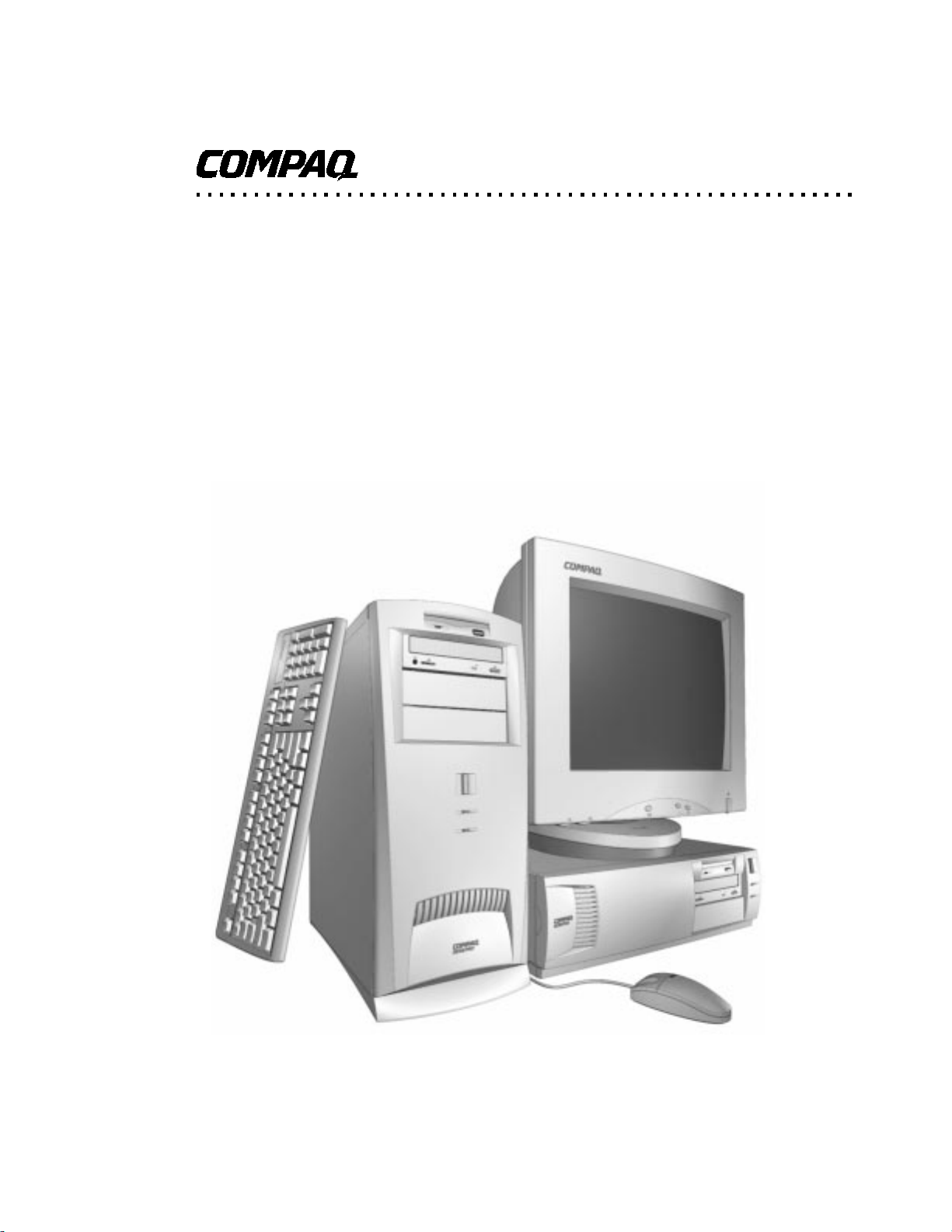
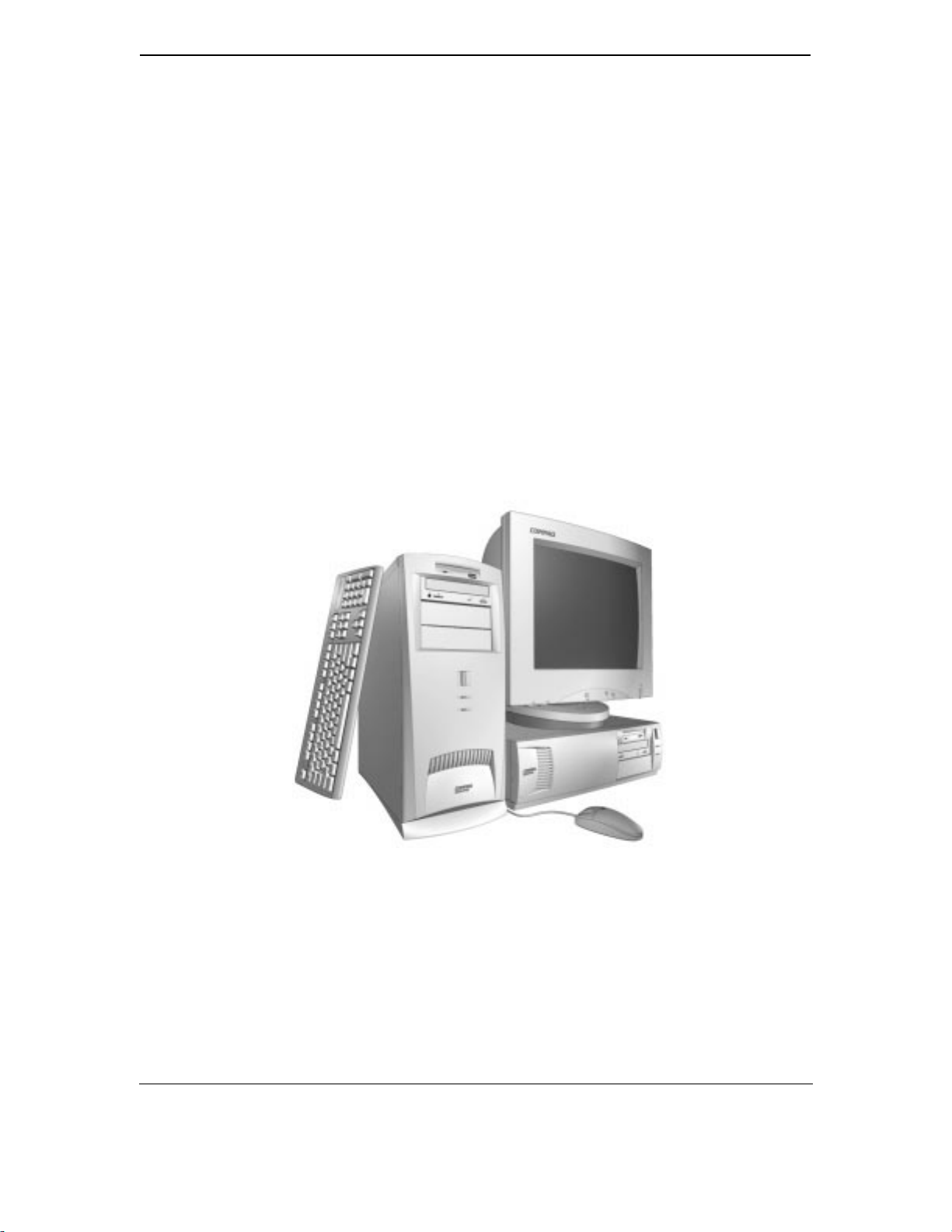
The Compaq Deskpro EN Series of desktop and minitower Personal Computers (Figure 2-1)
delivers an outstanding combination of manageability, serviceability, and consistency for
enterprise environments. Based on Intel Pentium II and Celeron processors, the Deskpro EN
Series emphasizes performance and industry compatibility. These models feature architectures
incorporating the PCI, AGP, and ISA buses. All m odels are easily upgradable and expan d a ble to
keep pa ce with the need s of t he office ent erpr ise.
Figure 2–1.
This chapter includes the following topics:
♦ Features and options (2.2) page 2-2
♦ Mechanical design (2.3) page 2-4
♦ System architectur e (2.4) page 2-8
♦ Specifications (2.5) page 2-13
Compaq Deskpro EN Series of Personal Computers
Desktop and Minitower Form Factors
Compaq Deskpro EN Desktop Personal Computers with Monitor
Third Edi tion - September 1998
2-1
Page 23

Chapter 2 System Overview
2.2 FEATURES AND OPTIONS
This section describes the standard features and available options.
2.2.1 STANDARD FEATURES
The following standard features are included on all models:
♦ Pentium II or Celeron processor
♦ High-per form ance 2D/3D AGP graphics card
♦ Embedded 16-bit full-duplex audio with Compaq Premier Sound
♦ 3.5 inch, 1. 44-MB diskette drive
♦ Extended IDE controller support for up to four IDE drives
♦ Hard drive fault prediction
♦ Two serial interfaces
♦ Parallel interface
♦ Two universal serial bus ports
♦ Two PCI slots
♦ Two combo PCI/ISA s lots
♦ 10/100 NIC card
♦ Compaq Enhanced keyboard w/Windows support
♦ Mouse
♦ APM 1.2 power management support
♦ Plug ’n Play compatible (with ESCD support)
♦ Intelligent Manageability support
♦ Energy Star compliant
♦ Security features including:
• Flash ROM Boot Bl oc k
• Diskette drive disable, boot disable , write p rotec t
• Power-on password
• Administrator password
• QuickLock/QuickBlank
• Smart Cover lock
• Smart Cover removal sense
• Serial port disable
• Parallel port disable
Compaq Deskpro EN Series of Personal Computers
2-2
Desktop and Minitower Form Factors
Third Edi tion – September 1998
Page 24

2.2.2 OPTIONS
The following items are available as options for all models and may be included in the standard
configuration of some models:
♦ System Memory: 16-MB DIMM (ECC and non-ECC)
♦ Hard drives/controllers: 3.2 GB UATA
♦ Removeable media drives:1.44 MB diskette drive
Technical Reference Guide
32-MB DIMM (ECC and non-ECC)
64-MB DIMM (ECC and nonECC)
128-MB DIMM (ECC and non-ECC)
4.3 GB Wide Ultra SCSI
9.1 GB Wide Ultra SCSI
Wide Ultra SCSI PCI controller
6.4 GB UATA
32x CD-ROM drive
PS-120 Power Drive
♦ Communications cards: Compaq 10/100TX PCI Intel with WOL UTP
Netelligent 10/100, TX PCI UTP TLAN
3COM Fast EtherLink XL 10/100TX PCI
Compaq Netelligent 56.6 Baud ISA Modem
♦ Graphics cards/memory: ATI RAGE PRO Turbo AGP card
ATI RAGE PRO Turbo AGP 2X card
4-MB SGRAM SODIMM (for RAGE PRO AGP 2X card)
Matrox MGA-G100A car d
Matrox Millennium G200-SD card
8-MB SDRAM SODIMM (for Millennium G200-SD card)
Compaq Deskpro Computers are easily upgraded and enh a nced with peripheral devices designed
to meet PCI and ISA standards. The Compaq Deskpro Personal Computers are compatible with
peripherals designed for Plug ’n Play operation.
Compaq Deskpro EN Series of Personal Computers
Desktop and Minitower Form Factors
Third Edi tion - September 1998
2-3
Page 25
Chapter 2 System Overview
2.3 MECHANICAL DESIGN
The Compaq Deskpro EN Series uses a desktop form factor. This section illustrates the
mechanical particulars of the bezel, chassis, and major board assemblies.
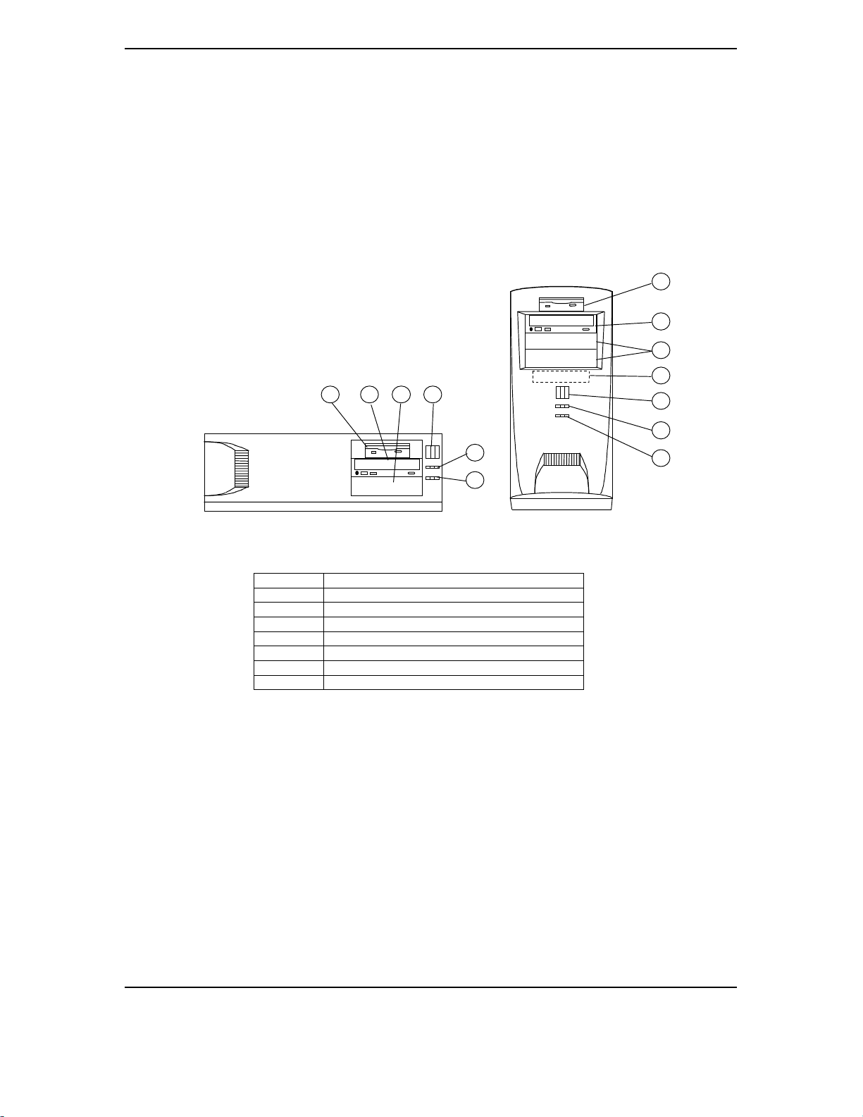
2.3.1 CABINET LAYOUTS
1
2
3
4
31 52
6
7
5
6
7
Figure 2–2.
Desktop Minitower
Item Function
1 1.44 MB Diskette Drive (5.25” drive bay)
2 CD-ROM Drive (CDS models) (5.25“ drive bay)
3 Internal Drive (5.25”) bay
4 Internal Drive (3.5”) bay
5 Power Button
6 Power On/Sleep Indicator
7 Hard Drive Activity Indicator
Cabinet La youts, Front View
Compaq Deskpro EN Series of Personal Computers
2-4
Desktop and Minitower Form Factors
Third Edi tion – September 1998
Page 26
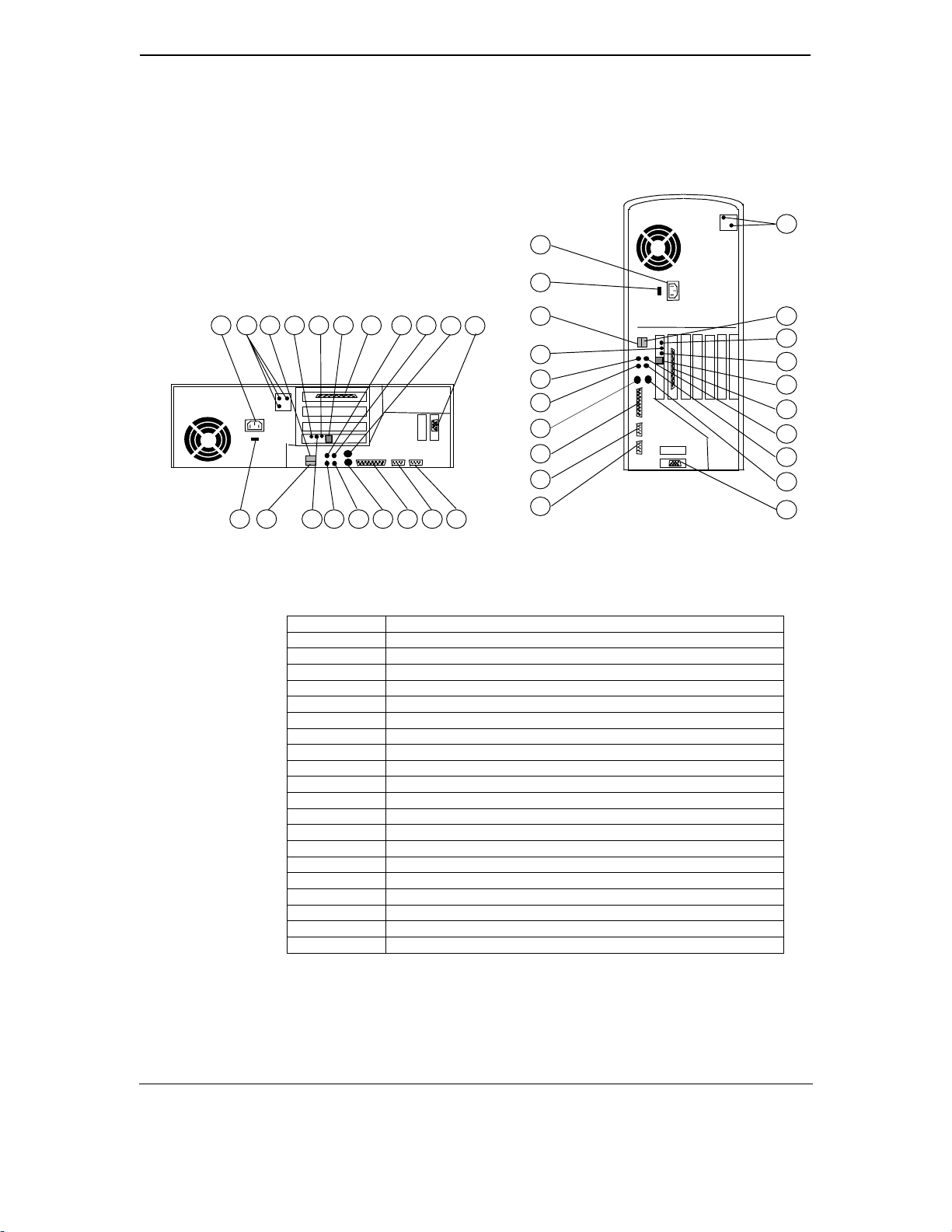
Technical Reference Guide
2
1
3
7
8
11 13
94
10 12 14
15
17 18 19
2
1 16
3 5
6
Desktop
Item Function
1 AC Line In Connector
2 Smart Cover Lock Screws
3 Line Voltage Switch
4 USB Interface Port B
5 USB Interface Port A
6 100TX speed LED
7 Activity LED
8Link LED
9 NIC Connector
10 SCSI connector
11 Audio Headphone Input
12 Audio Microphone Input
13 Audio Line Output
14 Audio Line Input
15 Keyboard Connector
16 Mouse Connector
17 Parallel Interface Connector
18 Serial Interface Connector (COM1)
19 Serial Interface Connector (COM2)
20 Graphics Monitor Connector
20
11
13
15
17
18
19
5
7
4
6
8
9
10
12
14
16
20
Minitower
Figure 2–3. Cabinet Layouts, Rear View
Compaq Deskpro EN Series of Personal Computers
Desktop and Minitower Form Factors
Third Edi tion - September 1998
2-5
Page 27
Chapter 2 System Overview
2.3.2 CHASSIS LAYOUTS
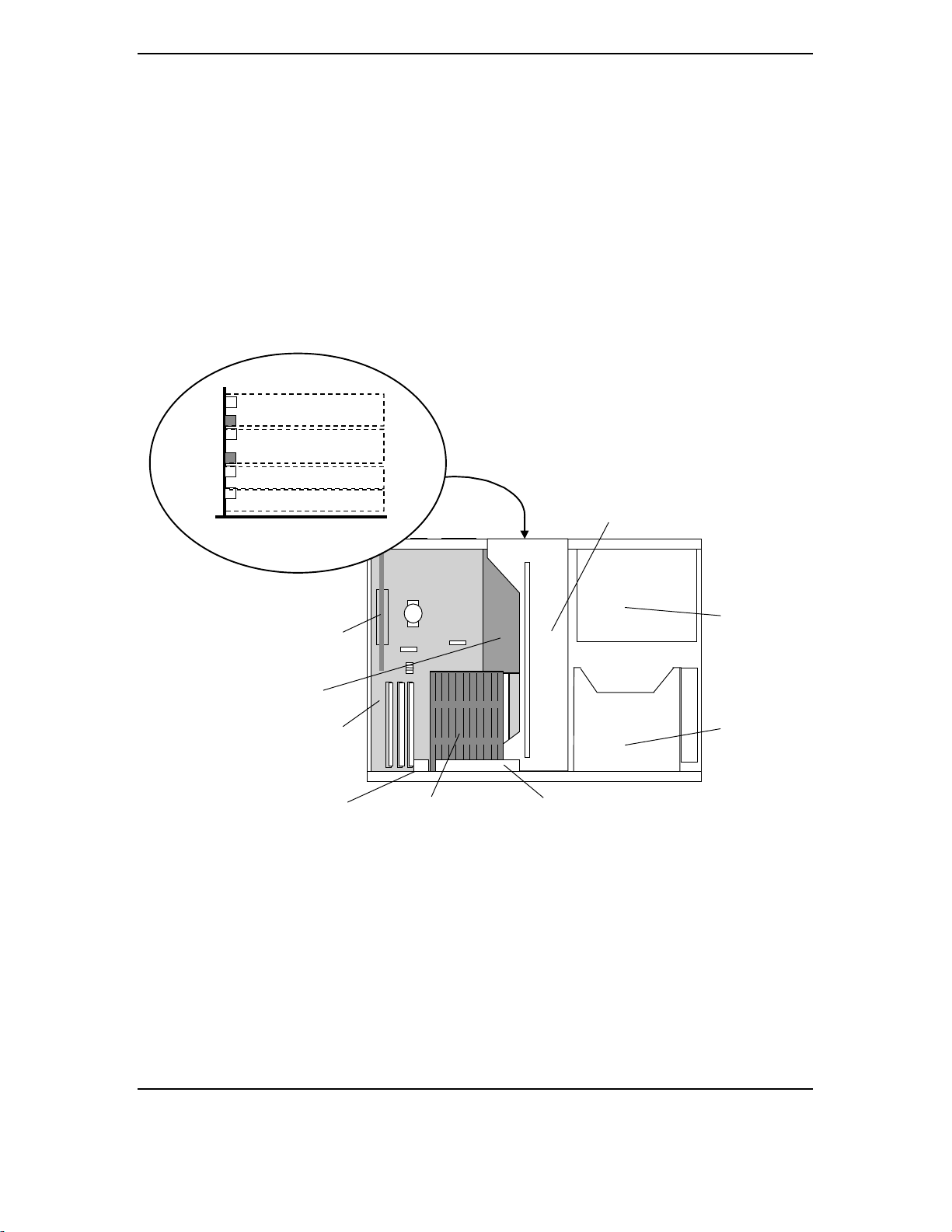
Figures 2-4 and 2-5 show the layout of key assemblies within the desktop and minitower chassis
respectively. For serviceability this system features an expansion card cage that allows easy
removal of the backplane and expansion cards as a single assembly. The tilt drive cage tilts up for
easy removal/replacement of drives. For detailed information on servicing the chassis refer to the
multimedia training CD-ROM and/or the maintenance and service guide for this system.
PCI Slot 4 (SCSI Card)
ISA Slot
PCI Slot 3
ISA Slot
PCI Slot 2
PCI Slot 1 (NIC Card)
Slots On Backplane,
Rear View
Back
Expansion Card Cage
AGP NLX
Graphics Card
Wide-Ultra
SCSI Card
System Board
Figure 2–4.
Speaker
Processor
Desktop Chassis Layout, Top View
Power Supply
Tilt Drive Cage
Chassi s Fan
Front
Compaq Deskpro EN Series of Personal Computers
2-6
Desktop and Minitower Form Factors
Third Edi tion – September 1998
Page 28
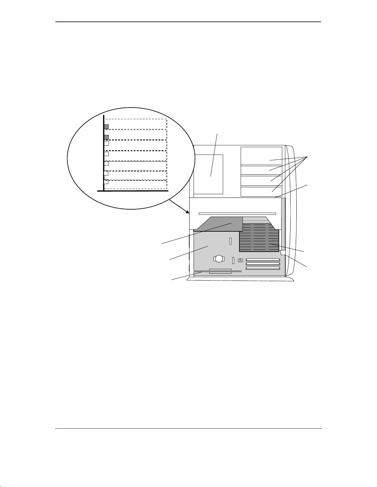
Technical Reference Guide
ISA Slot
ISA Slot
PCI Slot 5
PCI Slot 4
PCI Slot 3
PCI Slot 1 (NIC Card)
Slots On Backplane,
Rear View @ 90
°
Wide-Ultra
SCSI Card
System Board
AGP NLX
Graphics Card
Power Supply
Drive Bays
Expansion Card Cage
Front
Back
Processor
Speaker
Figure 2–5. Minit ower Chassis Layout, Left Side View
Compaq Deskpro EN Series of Personal Computers
Desktop and Minitower Form Factors
Third Edi tion - September 1998
2-7
Page 29
Chapter 2 System Overview
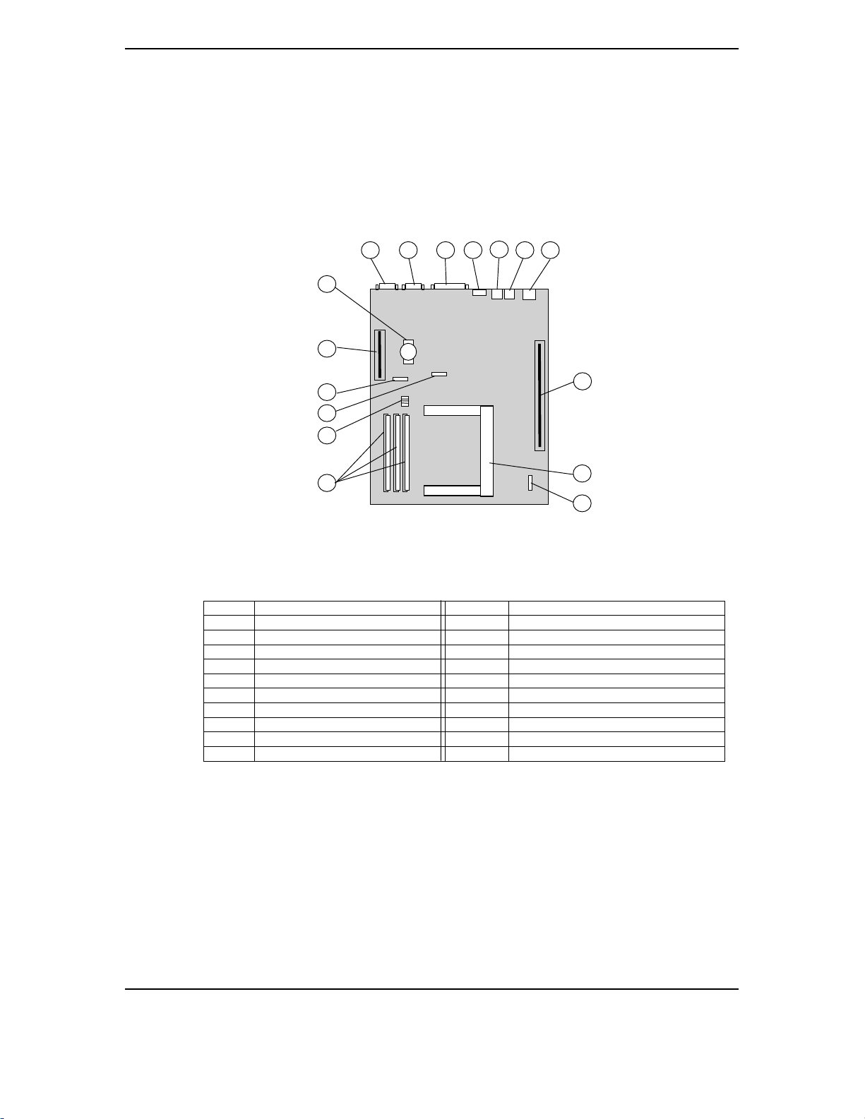
2.3.3 BOARD LAYOUTS
Figure 2-6 shows the location of connectors and switches for the system board, which is the same
for all models and both formfactors.
16
15
1 3
2
6 7
5
4
14
13
12
11
8
9
10
System Board (NLX-Type)
(P/N 007998-xxx
or 008123-xxx [1])
Item Function Item Function
1 Serial I/F (COM2) 7 (bottom) USB Port A I/F
2 Serial I/F (COM1) 8 Backplane Connector
3 Parallel I/F 9 Processor Slot 1
4 (top) Mouse connector 10 Heat Sink Thermal Diode Connector [2]
4 (bottom) Keyboard connector 11 DIMM Sockets
5 (top) Audio Line Input 12 Frequency/Password DIP Switch
5 (bottom) Audio Line Output 13 Heat Sink Thermal Diode Connector [3]
6 (top) Audio Mic Input 14 CMOS Clear Jumper
6 (bottom) Audio Headphone Output 15 AGP Slot (NLX-type)
7 (top) USB Port B I/F 16 Battery
NOTE:
[1] T he two system boards are electrically identical. There are slight differences in the location of some
components. Later production units use the 008123-xxx board.
[2] PCA # 008123
[3] PCA # 007998
Figure 2–6.
Compaq Deskpro EN Series of Personal Computers
2-8
System Board Connector and Switch Locations
Desktop and Minitower Form Factors
Third Edi tion – September 1998
Page 30
Technical Reference Guide
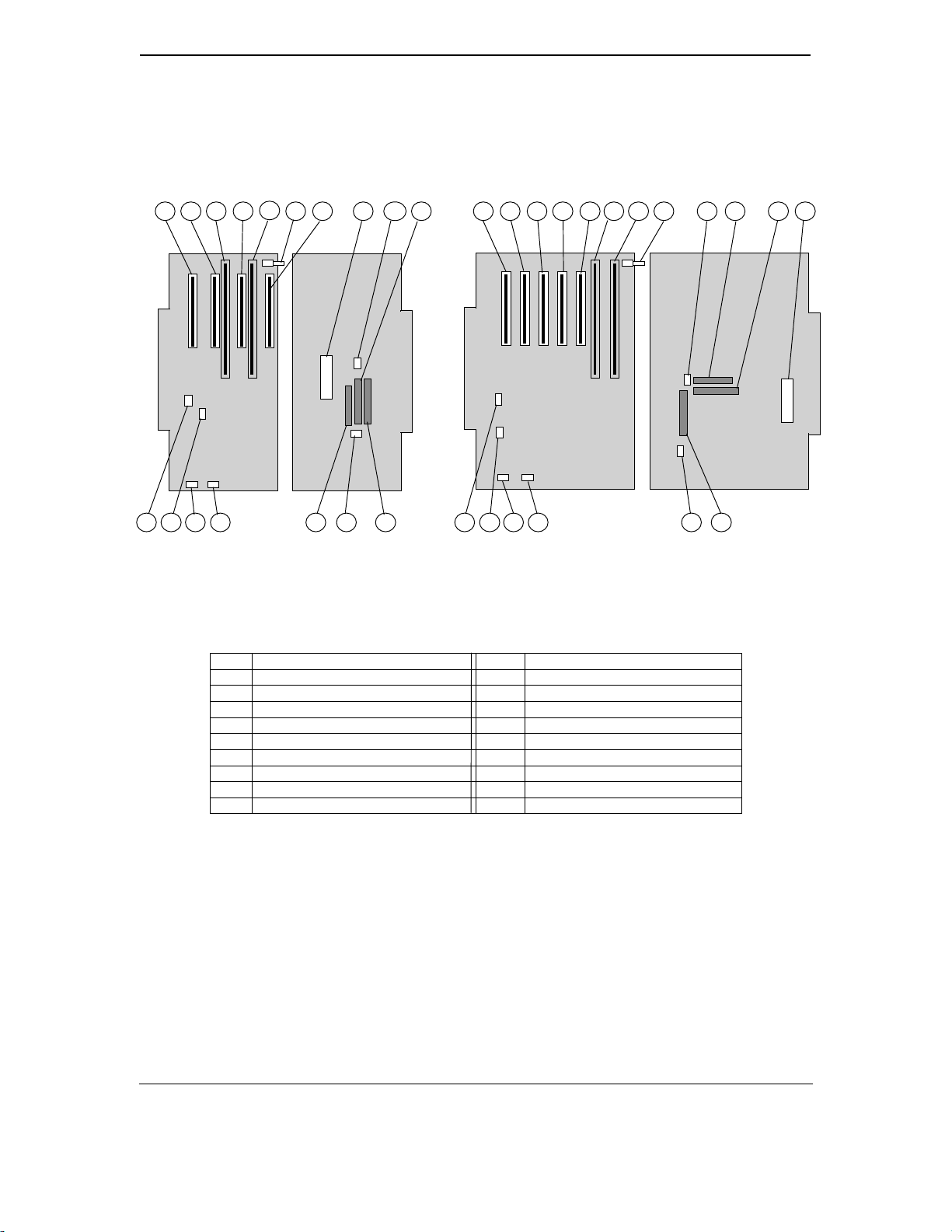
Figure 2-7 shows the connector and switch locations for the two types of backplane boards.
1 3
2 8
4
5
6 7
9
10
11
1 2
7 3 5 9
4
6
11
1210
15
16
17
18 131415161718
System Board Side Power Supply Side
14
1312
Desktop Backplane Boar d
(P/N 008001-xxx
or 009663-xxx [5])
Item Function Item Function
1 PCI connector J20 (slot 1) 10 CD audio input header P7
2 PCI connector J21 (slot 2) 11 Secondary EIDE connector P21
3 ISA connector J10 [1] 12 Diskette drive connector P10
4 PCI connector J22 (slot 3) [2] 13 Primary EIDE connector P20
5 ISA connector J11 [3] 14 Power button/LED header P5
6 Smart Cover sensor switch 15 Fan header P8
7 PCI connector J23 (slot 4) [4] 16 Speaker header P6
8 PCI connector J24 (slot 5) 17 SCSI LED header P29
9 Power supply connector P1 18 NIC WOL header P9
NOTES:
[1] Shares slot with item 4 on desktop backplane (combo slot 1)
[2] Shares slot with item 3 on desktop backplane (combo slot 1)
[3] Shares slot with item 7 on desktop backplane (combo slot 2)
[4] Shares slot with item 5 on desktop backplane (combo slot 2)
[5] Later production units use the 009663-001 board
Figure 2–7. Backplane Board Connector, Header, and Switch Locations
Power Supply SideSystem Board Side
Minitower Backplane Boar d
(P/N 008058-xxx)
Compaq Deskpro EN Series of Personal Computers
Desktop and Minitower Form Factors
Third Edi tion - September 1998
2-9
Page 31

Chapter 2 System Overview
2.4 SYSTEM ARCHITECTURE
The Compaq Deskpro EN Series of Personal Computers is based on an Intel Pentium II processor
matched with the Intel 440BX AGPset. The basic archi t ectur e (Figure 2-8), uses three main
buses: the Host bus, the Peripheral Component Int er conn ect (PCI) bus, and th e Industry Standard
Architect u re (ISA) bus.
The Host and memory buses provide high performance support for CPU, cache and system
memory accesses, and operate at 66 or 100 MHz, depending on the speed of the microprocessor.
The PCI bus provides support for the UATA controllers, USB ports, and PCI expansion devices.
The PCI bus operates a t 3 3 MHz. Thi s system also includes an Accelerat ed Graph ics Port (AGP)
slot for an AGP g raph i cs card. The AGP bus is closely associated with the PCI bus but operates at
66 MHz and allows data pipelining, sideband addressing, and frame mode transfers for increased
3D graphics performance.
The ISA bus provides a standard 8-MHz interface for the input/output (I/O) devices such as the
keyboard, diskette drive, serial and parallel interfaces, as well as the addition of 16- or 8-bit
expansion devices.
The nort h and south bri dge functi ons a re provided by the 440BX AGPset designed to compliment
the processor. The support chipset also provides memory controller and data buffering functions
as well as bus control and arbitration functions.
The I/O interfaces and diskette drive controller ar e integrated into the PC87307 I/O Contr oller.
This component also includes the real time clock and battery-backed configuration memory
(CMOS).
Table 2-1 lists differences between system models:
Table 2–1.
Model Differences
Table 2-1
.
Model Differences
Form Factor DT/MT DT/MT DT/M
CPU Speed (MHz) 266/300/333 333/350/400 300/333/350/400 400/450
Host Bus Speed (MHz) 66 66/100/100 66/66/100/100 100
Hard Drive 3.2 GB UATA 4.3 GB SCSI 6.4 GB UATA 9.1 GB SCSI
System Memory:
Standard
Maximum installable
Graphics Controller ATI RAGE PRO
NOTE:
Only BTO configurations shown.
Model 3200 Model 4300 Model 6400 Model 9100
16/32 MB SDRAM
384 MB
Turbo
AGP 1X Card
32/64 MB ECC
384 MB
ATI RAGE PRO
Turbo
AGP 2X Card
32/64 MB SDRAM
ATI RAGE PRO
AGP 1X/2X Card
384 MB
Turbo
T
MT
64 MB ECC
384 MB
ATI RAGE PRO
Turbo
AGP 2X Card
The following subsections provide a description of the key functions and subsystems.
Compaq Deskpro EN Series of Personal Computers
2-10
Desktop and Minitower Form Factors
Third Edi tion – September 1998
Page 32

Graphics
(2)
g
Cntlr. Card
66-MHz
32-Bit
AGP Bus
10/100 NIC
Card
Pentium II or
Processor
33-MHz
32-Bit
PCI Bus
Celeron
82443BX
(North
Bridge)
66-/100- MHz 64-Bit Host Bus
66-/100-MHz
64-Bit
System
Memory
Wide Ultra SCSI
Cntlr. Card
Technical Reference Guide
Wide Ultra
SCSI
Hard Drive
IDE
Hard Drive
Beep Audio
CD Audio
CDS Desktops and all Minitower models.
3200 and 6400 models only.
4300 and 9100 models only.
Audio
Subsystem
Keyboard/
Mouse I/F
Pri.
IDE I/F
Sec.
IDE I/F
87307 I/O Controller
Diskette
I/F
82371
(South
Bridge)
Serial
I/F
USB
I/F (2)
16-Bit ISA Bus
Parallel
I/F
System
Security
Lo
BIOS
ROM
ic
Power
Supply
Figure 2–8. Compaq Deskpro EN System Architecture, Block diagram
Compaq Deskpro EN Series of Personal Computers
2-11
Desktop and Minitower Form Factors
Third Edi tion - September 1998
Page 33

Chapter 2 System Overview
2.4.1 PROCESSOR
The Deskpro EN Series includes models based on Pentium II and Celeron processors. The
processor and heat sink is mounted as an assembly (Figure 2-9) in a slot (Slot 1) on the system
board. The Pentium II processor includes a microprocessor and a secondary (L2) cache contained
in a single edge connector (SEC) cartridge to which a heat sink is attached. The Celeron
processor includes a microprocessor mounted on a single edge processor package (SEPP) board.
On these systems the SEPP board of the Celeron processor is contained within a SEPP board
housing and heat sink.
Heat Sink
SEPP Board
SEC Cartridge
Microprocessor
Figure 2–9.
Secondary (L2) Cache
Pentium II Processor
Assembly
Processor Assembly Compari son
SEPP Board
Housing
Celeron Processor
Assembly
The Pentium II and Celeron processors are backward-compatible with software written for the
Pentium MMX, Pentium Pro, Pentium , a nd x86 micropr ocessors. The integra ted microprocessor
provides performance enhancements for multi-byte and floating-point processing.
Microprocessor
Compaq Deskpro EN Series of Personal Computers
2-12
Desktop and Minitower Form Factors
Third Edi tion – September 1998
Page 34

2.4.2 SYSTEM MEMORY
This system provides three 168-pin DIMM sockets with 16, 32 or 64 megabytes of RAM
installed depending on model. System memory can be expanded up to 384 megabytes using 16-,
32-, 64-, an d 128-MB DIMMs. T his system supports SDRAM, EDO, and E CC DIMMs. Models
3200 and 6400 come with SDRAM installed while models 4300 and 9100 come with ECC
DIMMs installed. Non-parity DIMMs are installed as standard but parity DIMMs are supported.
2.4.3 SUPPORT CHIPSETS
Table 2-2 shows the functions provided by the key components on the system board.
Technical Reference Guide
Table 2–2.
Support Chipsets
Table 2-2.
Support Chipsets
Component Name Component Type Function
PCI Arbitration Controller (PAC) North Bridge 82443BX Memory Controller
PCI-ISA/IDE eXcelerator (PIIX4E) South Bridge 82371 PCI/ISA Bridge
Super I/O Controller 87307 Keyboard I/F
Clock Generator CY2280 Clock Generator
System Security ASIC Compaq ASIC Super I/O Security
Host/PCI Bridge
EIDE Controller
DMA Controll er
Interrupt Controller
Timer/Counter
NMI Registers
Reset Control Reg.
USB I/F (2)
Diskette I/F
Serial I/F
Parallel I/F
RTC/CMOS Mem.
GPIO Ports
Smart Cover Lock
ROM Write Protect
Temperature Shutdown
SM/WOL Interrupts
Diskette Write Disable
Pwr LED Blink Cntrl.
PS On sig. Cntrl.
2.4.4 MASS STORAGE
All models include a 3.5 inch 1.44-MB diskette drive installed. Either an EIDE or SCSI hard
drive is also installed, depending on model. All models include a PCI bus mastering Enhanced
IDE (EIDE) controller that provides two EIDE interfaces supporting up to four IDE devices.
Models equipped with a SCSI drive include a Wide Ultra SCSI adapter board. A 32x CD-ROM is
included on desktop CDS models and on all MT models.
Compaq Deskpro EN Series of Personal Computers
Desktop and Minitower Form Factors
Third Edi tion - September 1998
2-13
Page 35

Chapter 2 System Overview
2.4.5 SERIAL AND PARALLEL INTERFACES
All models include two serial ports and a parallel port accessible at the rear of the chassis. The
serial and parallel ports are integrated into a PC87307 I/O Controller component. The serial port
is RS-232-C/16550-compatible and operates at baud rates up to 115,200. The parallel interface is
Enhanced Parallel Port (EPP1.9) and Enhanced Capability Port (ECP) compatible, and supports
bi-directional data transfers.
2.4.6 UNIVERSAL SERIAL BUS INTERFACE
All models feature two Universal Serial Bus (USB) ports that provide a high speed interface for
future systems and/or periph er a ls. The USB operates at 12 Mbps and provides hot
plugging/unplugging (Plug ’n Play) functionality.
2.4.7 GRAPHICS SUBSYSTEM
The graphics subsystem is conatained on a card installed into the AGP slot. Two types of
gra phics contr ol lers a re used, depend i ng on the microprocessor emp loyed on th e s ystem boa rd as
indicated in Ta ble 2-3.
Table 2–3.
Graphics Subsystem Comparison
Graphics Subsystem Comparison
Graphics Controller ATI Rage Pro Turbo AGP ATI Rage Pro Turbo AGP 2X
Graphics Memory
Standard installed:
Expandable to:
Maximum Resolution
w/ standard mem.
w/ max. mem.
266-/300-/333-MHz Processor 350-/400-/4500 MHz Processor
1600 x 1200 @ 65K colors
2.4.8 AUDIO SUBSYSTEM
All models feature the Compaq Premier Sound system. The system board includes an embedded
16-bit full-duplex subsystem based on the ES1869 graphics controller. T he audio output is
processed through a six-level equalizer designed to work with the chassis acoustics. A lowdistortion 5-watt amplifier drives a long-excursion speaker for optimum sound. The audio
subsystem is compatible with software written for industry-common sound hardware.
Table 2-3.
4 MB SGRAM
N/A
--
4 MB SGRAM
8 MB SGRAM
1600 x 1200 @ 65K colors
1600 x 1200 @ 16.7M colors
Compaq Deskpro EN Series of Personal Computers
2-14
Desktop and Minitower Form Factors
Third Edi tion – September 1998
Page 36

2.5 SPECIFICATIONS
This section includes the environmental, electrical, and physical specifications for the Compaq
DESKPRO EN Series Per sonal Comput ers.
Technical Reference Guide
Table 2–4.
Environmental Specifications
Table 2-4.
Environmental Specifications
Parameter Operating Nonoperating
Air Temperature 50
Shock N/A 60.0 g for 2 ms half-sine pulse
Vibration 0.000215g^ 2/hz, 10-300 Hz [1] 0.0005g^ 2/Hz, 10-500 Hz [1]
Humidity 90% RH @ 36
Maximum Altitude 10,000 ft (3048 m) 30,000 ft (9,144 m)
NOTE:
Table 2–5.
Values are subject to change without notice.
[1] 0.5 grms nominal
Electrical Specifications
o
to 95o F (10o to 35o C) -24o to 140o F (-30o to 60o C)
o
C (no hard drive) 95% RH @ 36o C
Table 2-5.
Electrical Specifications
Parameter U.S. International
Input Line Voltage:
Nominal:
Maximum:
Input Line Frequency Range:
Nominal:
Maximum:
Power Supply:
Maximum Continuous Power
Maximum Peak Power
Maximum Line Current Draw
110 - 120 VAC
90 - 132 VAC
50 - 60 Hz
47 - 63 Hz
200 watts
200 watts
5.5 A
200 - 240 VAC
180 - 264 VAC
50 - 60 Hz
47 - 63 Hz
200 watts
200 watts
3.0 A
Table 2–6.
Physical Specifications
Table 2-6.
Physical Specific ations
Parameter Desktop Minitower
Height 5.88 in (14.93 cm) 20.25 in (51.44 cm)
Width 19.16 in (48.66 cm) 8.38 in (21.29 cm)
Depth 16.82 in (42.72 cm) 18.60 in (47.24 cm)
Weight [1] 32.0 lb (14.50 kg) 40.0 lb (18.20 kg)
NOTES:
Metric figures in parenthesis.
[1] System weight may differ depending on installed drives/peripherals.
Compaq Deskpro EN Series of Personal Computers
Desktop and Minitower Form Factors
Third Edi tion - September 1998
2-15
Page 37

Chapter 2 System Overview
Table 2–7. Diskette Drive Specifications
Parameter Measurement
Media Type 3.5 in 1.44 MB/720 KB diskette
Height 1/3 bay (1 in)
Bytes per Sector 512
Secto rs per Track:
High Density
Low Density
Tracks p er Side:
High Density
Low Density
Read/Write Heads 2
Average Access Time:
Track-to-Track (high/low)
Average (high/low)
Settling Time
Latency Average
Table 2-7.
Diskette Drive S pec ifications
(Compaq SP# 179161-001)
18
9
80
80
3 ms/6 ms
94 ms/173ms
15 ms
100 ms
Table 2–8. 24x CD-ROM Drive Specifications
Table 2-8.
32x CD-ROM Drive Spec ifications
(SP# 327659-001)
Parameter Measurement
Interface Type IDE
Transfer Rate:
Max. Sustained
Burst
Media Type Mode 1,2, Mixed Mode, CD-DA,
Capacity:
Mode 1, 12 cm
Mode 2, 12 cm
8 cm
Center Hole Diameter 15 mm
Disc Diameter 8/12 cm
Disc Thickness 1.2 mm
Track Pitch 1.6 um
Laser
Beam Divergence
Output Power
Type
Wave Length
Average Access Time:
Random
Full Stroke
Audio Output Level 0.7 Vrms
Cache Buffer 128 KB
4800 KB/s
16.6 MB/s
Photo CD, Cdi , CD-XA
550 MB
640 MB
180 MB
53.5 +/- 1.5
53.6 0.14 mW
790 +/- 25 nm
<100 ms
<150 ms
°
GaAs
Compaq Deskpro EN Series of Personal Computers
2-16
Desktop and Minitower Form Factors
Third Edi tion – September 1998
Page 38

Technical Reference Guide
Table 2–9. Hard Drive Specifications
Table 2-9.
Hard Drive Specifications
Parameter
Interface EIDE-UATA Wide-Ultra SCSI EIDE-UATA Wide-Ultra SCSI
Drive Type 65 65 65 65
Drive Size 5.25 in 5.25 in 5.25 in 5.25 in
Transfer Rate 33.3 MB/s 40.0 MB/s 33.3 MB/s 40.0 MB/s
Seek Time (w/settling)
Single Track
Average
Full Stroke
Disk Format:
# of Cylinders
# of Data Heads
# of Sectors per Track
Buffer Size 256 KB 512 KB 256 KB 512 KB
Drive Fault Prediction SMART II SMART II SMART II SMART II
3.2 GB
(# 166873-001)
<1.0 ms
<9.7 ms
<18.0 ms
6697
15
63
4.3 GB
(# 179287-001)
.76 ms
7.5 ms
17.0 ms
8420
8
165-264
6.4 GB
(# 166973-001)
2.0 ms
<9.7 ms
20.0 ms
13325
15
63
9.1 GB
(# 179288-001)
.76 ms
7.5 ms
15.0 ms
8420
10
165-264
Compaq Deskpro EN Series of Personal Computers
Desktop and Minitower Form Factors
Third Edi tion - September 1998
2-17
Page 39

Chapter 2 System Overview
This page is intentionally blank.
Compaq Deskpro EN Series of Personal Computers
2-18
Desktop and Minitower Form Factors
Third Edi tion – September 1998
Page 40

Chapter 3
PROCESSOR/
MEMORY SUBSYSTEM
Technical Reference Guide
3.
3.1
Chapter 3 PROCESSOR/MEMORY SUB S YSTEM
INTRODUCTION
This chapter describes the processor/cache memory subsystem of the Compaq Deskpro EN Series
of desktop and minitower Personal Computers. These systems are shipped either with an Intel
Pentium II or Celeron processor and either 32 or 64 megabytes of system memory, depending on
configuration.
This chapter includes the following topics:
♦ Processor/memory subsystem [3.2] page 3-2
Compaq Deskpro EN Series of Personal Computers
Desktop and Minitower Form Factors
Third Edi tion - September 1998
3-1
Page 41

Chapter 3 Processor/Memory Subsystem
3.2 PROCESSOR/M EM O RY SUBSYSTEM
The subsystem features an Intel Pentium II or Celeron processor with the North Bridge
(82443BX), and either 32 or 64 megabytes of system memory (Figure 3-1). The 64-bit Host and
memory buses operate at either 66- or 100-MHz depending on the speed of the processor. The 32bit PCI bus operates at 33-MHz.
Processor
(in Slot 1)
J1
32-MB
DIMM
System Memory
J2
DIMM
J3
DIMM
Graphics
Subsystem
Optional module
Figure 3–1.
66-/100-MHz
64-Bit Host Bus
66-MHz
32-Bit
AGP Bus
(82443BX)
Cntl
66-/100-MHz
Mem. Data Bus
North
Bridge
Mem. Addr.
33-MHz 32-Bit PCI Bus
Processor/Memory Subsystem Archi t ectu re
The processor is mounted in a slot 1-type connector that facilitates easy changing/upgradin g.
Replacing the processor may require reconfiguring DIP switch SW1 to select the correct bus
frequency/core frequency combination. Frequency selection is described in detail later in this
section.
The North Bridge (82443BX) provides Host/memory/PCI bridge functions and controls data
transfers with system memory over the 64-bit memory data bus. The 443BX supports SDRAM,
EDO, FPM, a nd ECC DIMM m odules. Three DIMM sockets allow the system memory to be
expanded to 384 megabytes.
Compaq Deskpro EN Series of Personal Computers
3-2
Desktop and Minitower Form Factors
Third Edi tion - September 1998
Page 42

3.2.1 PROCESSOR
The system board includes a Slot 1-type interface that accommodates a Pentium II or Celeron
processor. Table 3-1 provides a comparison between the key parameters of the Pentium II and
Celeron processors.
Technical Reference Guide
Table 3–1.
CPU Freq. 266-333 MHz 300 MHz 300/333 MHz 350 MHz 400 MHz 450 MHz
L2 Cache 512 KB 0 KB 128 KB 512 KB 512 KB 512 KB
L2 Cache Freq. 133-166 MHz -- 300/333 MHz 175 MHz 200 MHz 225 MHz
Host Bus Freq. 66 MHz 66 MHz 66 MHz 100 MHz 100 MHz 100 MHz
Processor Comparison
Pentium II
266-333
3.2.1.1 Pentium II Processo r
The Intel Pentium II processor is packaged in a Single Edge Connector (SEC) cartridge that
contains the microprocessor and a 512-KB ECC secondary (L2) cache. The processor’s
archit ectur e (Figur e 3-2) includes a dual-ALU MMX-supporting CPU, branch prediction logic,
dual-pipeline floating point unit (FPU) coprocessor, and a 32-KB L1 cache that is split into two
16-KB 4-way, set-associative caches for handling code and data separately. These functions
operate at core processing speed (Figure 3-2), which ran ges from 266 to 400 megahertz
depending on version.
Table 3-1.
Processor Comparsion
Celeron
266/300
Pent ium II Processor
Celeron
300A/333
Pentium II
350
Pentium II
400
Pentium II
450
CPU
Branch
Prediction
Core processing speed ½ Core processing speed
Figure 3–2.
Pentium II Processor Internal Architecture
FPU 32-KB
FSB
I/F
L1
Cache
512-KB
L2
Cache
Host bus speed
The Pentium II processor includes 512 kilobytes of SRAM for the write-through L2 cache.
Accesses with the L2 cache occur at 50% of the core processing speed. The front side bus (FSB,
also referred to as the Host bus) interface of the 266-, 300-, an d 333-MHz processors operates at
66-MHz. The FSB interface of the 350- and 400-MHz processors operates at 100 MHz. The
Pentium II processor is software-compatible with earlier generation x86 microprocessors.
NOTE:
Later versions of the Pentium II processor require updated BIOS firmware.
Refer to section 3.2.2 for upgrading information.
Compaq Deskpro EN Series of Personal Computers
Desktop and Minitower Form Factors
Third Edi tion - September 1998
3-3
Page 43

Chapter 3 Processor/Memory Subsystem
3.2.1.2 Celeron Processor
Select systems are shipped with the Intel Celeron processor. The Celeron processor (Figure 3-3)
uses a CPU/FPU core that is functionally the same as that of the Pentium II described previously
and provides the same level of branch prediction, math co-processing, MMX support, and L1
cache operation. Processing and Host bus speed ratios follow those of the Pentium II processors
and are set and deter mi ned with the same methods. Note that the Celeron 300 does not include
an L2 cache. The L2 cache of the Celeron 300A and 333 operates at processor (CPU) speed.
Cele ron Processor
CPU
Branch
Prediction
[1] Not present on Celeron 266 or 300 processors.
Core processing speed
Host bus speed
Figure 3–3.
Celeron Processor Internal Architecture
FPU
FSB
I/F
32-KB
L1
Cache
128-KB
L2
Cache [1]
Like the Pentium II processor, the Celeron processor is software-compatible with earlier
generation Pentium MMX, Pentium , a nd x86 processors.
NOTE:
Later versions of the Celeron processor require updated BIOS firmware. Refer
to section 3.2.2 for upgrading information.
Compaq Deskpro EN Series of Personal Computers
3-4
Desktop and Minitower Form Factors
Third Edi tion - September 1998
Page 44

3.2.2 PROCESSOR CHANGING/UPGRADING
The slot 1 design allows for easy changing and/or upgradin g of the processor/cache complex.
Changing the processor requires disconnection/re-connection of the heat sink sensor cable and
may require upgrading the BIOS firmware and re-configuration of the bus/core speed switch
discussed in the following paragraphs.
3.2.2.1 BIOS Upgrading
The Pentium II 450 an d Celeron 300A/333 processors require BIOS firmware dated 7/30/98 or
later. Installing and running one of these processors in a system with BIOS dated earlier than
7/30/98 will likely cause the system to halt (lockup).
The BIOS (ROM) version may be checked using either the Compaq Diagnostics or Compaq
Insight utility.
3.2.2.2 Processor Speed Selection
Technical Reference Guide
Changing the processor may require re-configuration of the bus/core frequency ratio. The system
board includes a six-position DIP switch (SW), of which positions 2-5 are read by the processor
(while RESET- is active) to select the bus-to-core frequency ratio. Table 3-2 shows the possible
switch configurations for this system and the resultant core (or processing) frequency, based on
the fron t side bus (FSB or Host bus) frequency.
Table 3–2.
Bus/Core Speed Switch Settings
Table 3-2.
Bus/Core Speed Swit c h S ettings
DIP SW1 Settings
2 3 4 5 [1]
1 0 0 0 1/3 200 300
1 1 0 0 2/7 233 350
0 0 1 0 1/4 266 400
0 1 1 0 2/9 300 450
1 0 1 0 1/5 333 500
NOTES:
Shipping configurations are unshaded.
[1] 0 = Switch Closed (On), 1 = Switch Open (Off)
The DIP switch settings should be set to match the processor installed.
Configuring for a speed higher than that which the processor is
designed could result in unreliable operation and possible system damage.
Bus/Core
Freq. Ratio w/66-MHz FSB w/100-MHz FSB
Core Frequency
The processor sets the clock generator to the appropriate bus frequency. Software can determine
the operating speed by reading the bus speed from an MSR register in the processor.
Compaq Deskpro EN Series of Personal Computers
Desktop and Minitower Form Factors
Third Edi tion - September 1998
3-5
Page 45

Chapter 3 Processor/Memory Subsystem
3.2.3 SYSTEM MEMORY
The system board contains three 168-pin DIMM sockets for system memory. This system is
designed for u si ng SDRAM or ECC DIMMs. As shipped fr om t he factory the standar d
configuration has 16, 32, or 64 megabytes of memory installed. The system memory is
expandable up to a maximu m of 384 megabytes. Single or double-sided DIMMs may be used. In
expanding the standard memory using modules from third party suppliers the following DIMM
type is recommended:
with a data access time (clock-to-data out) of 9.0 ns or less @ CL=2 or CL=3
66- or 100-MHz unbuffered RAM supporting CAS latency (CL) 2 or 3
.
NOTE:
The DIMM speed should compliment the host bus speed of the processor (i.e.,
use 66-MHz DIMMs in a system with a 266/66 pr ocessor and 100-MHz DIMMs in a
system with a 350/100 processor). All systems are factory-shipped with 100-MHz
DIMMs.
The RAM type and operating parameters are detected during POST by the system BIOS usin g the
serial presence detect (SPD) method. T his method employs an I
2
C bus to communicate with an
EEPROM on each installed DIMM. The EEPROM holds the type and operating parameter data.
The supported format complies with the JEDEC specification for 128-byte EEPROMs. Thi s
system also provides support for 256-byte EEPROMs to include additional Compaq-added
features such as part number and serial number. The SPD format as supported in this system is
shown in Table 3-3.
The key SPD bytes that BIOS checks for compatibility are 2, 9, 10, 18, 23, and 24.
If BIOS
detects EDO DIMMs a “memory incompatible” message will be displayed and the system
will halt.
If ECC DIMMs are used, all DIMMs installed must be ECC for ECC benefits (error
logging) to be realized.
Once BIOS determines the DIMM type the DRAM speed and CAS latency is checked based on
the following criteria:
Access
from
Bus Speed Cycle Time
Clock
66 MHz 15 ns 9 ns @ 50 pf loading
100 MHz 10 ns 6 n s @ 50 pf loaldin g
NOTE:
Refer to chapter 8 for a description of the BIOS procedure of interrogating
DIMMs.
Only CAS latencies of 2 or 3 are supported. If DIMMs with u nequal CAS latencies are installed
then operation will occur based on the DIMM with the greatest latency.
If an incompatible DIMM is detected the NUM LOCK will blink for a short period of time during
POST and a n err or message may or may not be displayed before the system ha ngs.
The system memory map is shown in Figure 3-3.
Compaq Deskpro EN Series of Personal Computers
3-6
Desktop and Minitower Form Factors
Third Edi tion - September 1998
Page 46

Technical Reference Guide
Table 3–3. SPD Addr ess Map ( SDRAM DIMM)
Table 3-3.
SPD Address Map (SDRAM DIMM)
Byte Description Notes Byte Description Notes
0 No. of Bytes Written Into EEPROM [1] 27 Min. Row Prechge. Time [7]
1 Total Bytes (#) In EEPROM [2] 28 Min. Row Active to Delay [7]
2 Memory Type 29 Min. RAS to CAS Delay [7]
3 No. of Row Addresses On DIMM [3] 30, 31 Reserved
4 No. of Column Addresses On DIMM 32..61 Superset Data [7]
5 No. of Module Banks On DIMM 62 SPD Revision [7]
6, 7 Data Width of Module 63 Checksum B ytes 0-62
8 Voltage Interface Standard of DIMM 64-71 JEP-106E ID Code [8]
9 Cycletime @ Max CAS Latency (CL) [4] 72 DIMM OEM Location [8]
10 Access From Clock [4] 73-90 OEM’s Part Number [8]
11 Config. Type (Parity, Nonparity, etc.) 91, 92 OEM’s Rev. Code [8]
12 Refresh Rate/Type [4] [5] 93, 94 Manufacture Date [8]
13 Width, Primary DRAM 95-98 OEM’s Assembly S/N [8]
14 Error Checking Data Width 99-125 OEM Specific Data [8]
15 Min. Clock Delay [6] 126, 127 Reserved
16 Burst Lengths Supported 128-131 Compaq header “CPQ1” [9]
17 No. of Banks For Each Mem. Device [4] 132 Header checksum [9]
18 CAS Latencies Supported [4] 133-145 Unit serial number [9] [10]
19 CS# Latency [4] 146 DIMM ID [9] [11]
20 Writ e Latency [4] 147 Checksum [9]
21 DIMM Attributes 148-255 Reserved [9]
22 Memory Device Attributes
23 Min. CLK Cycle Time at CL X-1 [7]
24 Max. Acc. Time From CLK @ CL X-1 [7]
25 Min. CLK Cycle Time at CL X-2 [7]
26 Max. Acc. Time From CLK @ CL X-2 [7]
NOTES:
[1] Programmed as 128 bytes by the DIMM OEM
[2] Must be programmed to 256 bytes.
[3] High order bit defines redundant addressing: if set (1), highest order RAS# address must be
re-sent as highest order CAS# address.
[4] Refer to memory manufacturer’s datasheet
[5] MSb is Self Refresh flag. If set (1), assembly supports self refresh.
[6] Back-to-back random column addresses.
[7] Field format proposed to JEDEC but not defined as standard at publication time.
[8] Field specified as optional by JEDEC but required by this system.
[9] Compaq usage. This system requires that the DIMM EEPROM have this
space available for reads/writes.
[10] Serial # in ASCII format (MSB is 133). Intended as backup identifier in case vender data is invalid.
Can also be used to indicate s/n mismatch and flag system adminstrator of possible system
Tampering.
[11] Contains the socket # of the module (first module is “1”). Intended as backup identifier (refer to
note [10]).
Compaq Deskpro EN Series of Personal Computers
Desktop and Minitower Form Factors
Third Edi tion - September 1998
3-7
Page 47

Chapter 3 Processor/Memory Subsystem
(
)
(
)
Figure 3-3 shows the system memory map for the system.
Host,
PCI, AGP Area
Host, PCI,
ISA Area
DOS Compatibility
Area
FFFF FFFFh
FFE0 0000h
FFDF FFFFh
FEC1 0000h
FEC0 FFFFh
FEC0 0000h
FEBF FFFFh
4000 0000h
3FFF FFFFh
0100 0000h
00FF FFFFh
0010 0000h
000F FFFFh
000F 0000h
000E FFFFh
000E 0000h
000D FFFFh
000C 0000h
000B FFFFh
000A 0000h
0009 FFFFh
0008 0000h
0007 FFFFh
High BIOS Area
2 MB
PCI Memory
(18 MB)
APIC Config. Space
(64 KB)
PCI Memory
Expansion
(2548 MB)
Host/PCI Memory
Expansion
(1008 MB)
Extended Memory
15 MB
System BIOS Area
(64 KB)
Extended BIOS Area
(64 KB)
Option ROM
(128 KB)
Graphics/SMRAM
RAM (128 KB)
Fixed Mem. Area
(128 KB)
4 GB
1 GB
16 MB
1 MB
640 KB
512 KB
Base Memory
(512 KB)
0000 0000h
NOTE: All locations in memory are cacheable. Base memory is always mapped to DRAM. The next 128 KB fixed
memory area can, through the north bridge, be mapped to DRAM or to PCI space. Graphics RAM area is mapped
to PCI or AGP locations.
Figure 3–4. System Memory Map
Compaq Deskpro EN Series of Personal Computers
3-8
Desktop and Minitower Form Factors
Third Edi tion - September 1998
Page 48

3.2.4 SUBSYSTEM CONFIGURATION
The 443BX north bridge component provides the configuration function for the
processor/memory subsystem. Table 3-4 lists the configuration registers used for setting and
checking such parameters as memory control and PCI bus operation. These registers reside in the
PCI Configuration Space and accessed using the methods described in Chapter 4, section 4.2.
Technical Reference Guide
Table 3–4.
Host/PCI Bridge Configuration Registers (443BX, Function 0)
Table 3-4.
Host/PCI B r idge Configuration Registers ( 82443B X , Function 0)
PCI Config.
Addr. Register
00, 01h Vender ID 8086h 6A, 6Bh DRAM Control Reg. 00h
02, 03h Device ID 7190h 6C..6Fh Memory Buffer Strength 55h
04, 05h Command 0006h 70h Multi-Transaction Timer 00h
06, 07h Status 0210h 71h CPU Latency Timer 10h
08h Revision ID -- 72h SMRAM Control 02h
09..0Bh Class Code -- 90h Error Command 00h
0Dh Latency Timer 00h 91h Error Status Register 0 00h
0Eh Header Type 00h 92h Error Status Register 1 00h
10..13h Aperture Base Config. 8 93h Reset Control 00h
50, 51h PAC Config. Reg. 00h A0..A3h AGP Capability Identifier N/A
53h Data Buffer Control 83h A4..A7h AGP Status N/A
55..56h DRAM Row Type 00h A8..ABh AGP Command 00h
57h DRAM Control 01h B0..B3h AGP Control 00h
58h DRAM Timing 00h B4h Aperture Size 0000h
59..5Fh PAM 0..6 Registers 00h B8..BBh Aperture Translation Table 0000h
60..67h DRAM Row Boundary 01h BCh Aperture I/F Timer 00h
68h Fixed DRAM Hole 00h BDh Low Priority Timer 00h
NOTES:
Refer to Intel Inc. documentation for detailed description of registers.
Assume unmarked locations/gaps as reserved.
Reset
Value
PCI Config.
Addr. Register
Reset
Value
Compaq Deskpro EN Series of Personal Computers
Desktop and Minitower Form Factors
Third Edi tion - September 1998
3-9
Page 49

Chapter 3 Processor/Memory Subsystem
This page is intentionally blank.
Compaq Deskpro EN Series of Personal Computers
3-10
Desktop and Minitower Form Factors
Third Edi tion - September 1998
Page 50

Chapter 4
SYSTEM SUPPORT
4. Chapter 4 SYSTEM SUPPORT
Technical Reference Guide
4.1
INTRODUCTION
This chapter covers subjects dealing with basic system architecture and covers the following
topics:
♦ PCI bus overview (4.2) page 4-2
♦ AGP bus overview (4.3) page 4-11
♦ ISA bus overview (4.4) page 4-16
♦ System clock distribution (4.5) page 4-28
♦ Real-time clock and configuration memory (4.6)page 4-29
♦ I/O map and r egister a ccessing (4.7) page 4-46
♦ System management (4. 8) page 4-51
This chapter covers functions provided by off-the-shelf chipsets and therefore describes only basic
aspects of these functions as well as information unique to the Compaq Deskpro EN Series of
Personal Computers. For detailed information on specific components, refer to the applicable
manufacturer’s documentation.
Compaq Deskpro EN Series of Personal Computers
Desktop and Minitower Form Factors
Third Edi tion - September 1998
4-1
Page 51

Chapter 4 System Support
y
4.2 PCI BUS OVERVIEW
NOTE:
This section describes the PCI bus in general and highlights bus
implementation in this particular system. For detailed information regarding PCI bus
operation, refer to the PCI Local Bus Specification Revision 2.1.
This system implements a 5-V, 32-bit Peripheral Component Interconnect (PCI) bus operating at
33 MHz. The PCI bus uses a shared address/data bus design. On the first clock cycle of a PCI bus
transaction the bus carries address information. On subsequent cycles, the bus carries data. PCI
transactions occur synchronously with the Host bus at 33 MHz. All I/O transactions involve the
PCI bus. All ISA transactions involving the microprocessor, cache, and memory also involve the
PCI bus. Memory cycles will involve the PCI if the access is initiated by a device or subsystem
other than the microprocessor.
The PCI bus handles address/data transfers through the identification of devices and functions on
the bus (Figure 4-1). A device is defined as a component or slot that resides on the PCI bus. A
function is defined as the end source or target of the bus transaction. A device (component or
slot) may contain one or more functions (i.e., in this system the PCI/ISA Bridge function, EIDE
controller function, USB function, and ACPI function are contained within the South Bridge
component).
Host Bus
PCI Connector Slot 5
PCI Connector Slot 4
Minitower onl
Figure 4–1.
82443 North Bridge
Host/PCI
Bridge
Function
PCI/ISA
Bridge
Function
PCI/AGP
Bridge
Function
32-Bit PCI Bus
EIDE
Controller
Function
82371 South Bridge
ISA Bus
PCI Bus Devices and Functions
USB
I/F
Function
PCI Connector Slot 3
PCI Connector Slot 2
PCI Connector Slot 1
Power
Manage
Function
Compaq Deskpro EN Series of Personal Computers
4-2
Desktop and Minitower Form Factors
Third Edi tion - September 1998
Page 52

4.2.1 PCI CONNECTOR
Technical Reference Guide
B94
A94
Figure 4–2.
Table 4–1.
B49
A49
A62
B62
B52
A52
PCI Bus Connector (32-Bit Type)
PCI Bus Connector Pinout
B1
A1
Table 4-1.
PCI Bus Connector P inout
Pin B Signal A Signal Pin B Signal A Signal Pin B Signal A Signal
01 -12 VDC TRST- 32 AD17 AD16 63 Reserved GND
02 TCK +12 VDC 33 C/BE2- +3.3 VDC 64 GND C/BE7-
03 GND TMS 34 GND FRAME- 65 C/BE6- C/BE5-
04 TDO TDI 35 IRDY- GND 66 C/BE4- +5 VDC
05 +5 VDC +5 VDC 36 +3.3 VDC TRDY- 67 GND PAR64
06 +5 VDC INTA- 37 DEVSEL- GND 68 AD63 AD62
07 INTB- INTC- 38 GND STOP- 69 AD61 GND
08 INTD- +5 VDC 39 LOCK- +3.3 VDC 70 +5 VDC AD60
09 PRSNT1- Reserved 40 PERR- SDONE 71 AD59 AD58
10 RSVD +5 VDC 41 +3.3 VDC SBO- 72 AD57 GND
11 PRSNT2- Reserved 42 SERR- GND 73 GND AD56
12 GND GND 43 +3.3 VDC PAR 74 AD55 AD54
13 GND GND 44 C/BE1- AD15 75 AD53 +5 VDC
14 RSVD Reserved 45 AD14 +3.3 VDC 76 GND AD52
15 GND RST- 46 GND AD13 77 AD51 AD50
16 CLK +5 VDC 47 AD12 AD11 78 AD49 GND
17 GND GNT- 48 AD10 GND 79 +5 VDC AD48
18 REQ- GND 49 GND AD09 80 AD47 AD46
19 +5 VDC PME- 50 Key Key 81 AD45 GND
20 AD31 AD30 51 Key Key 82 GND AD44
21 AD29 +3.3 VDC 52 AD08 C/BE0- 83 AD43 AD42
22 GND AD28 53 AD07 +3.3 VDC 84 AD41 +5 VDC
23 AD27 AD26 54 +3.3 VDC AD06 85 GND AD40
24 AD25 GND 55 AD05 AD04 86 AD39 AD38
25 +3.3 VDC AD24 56 AD03 GND 87 AD37 GND
26 C/BE3- IDSEL 57 GND AD02 88 +5 VDC AD36
27 AD23 +3.3 VDC 58 AD01 AD00 89 AD35 AD34
28 GND AD22 59 +5 VDC +5 VDC 90 AD33 GND
29 AD21 AD20 60 ACK64- REQ64- 91 GND AD32
30 AD19 GND 61 +5 VDC +5 VDC 92 Reserved Reserved
31 +3.3 VDC AD18 62 +5 VDC +5 VDC 93 Reserved GND
-- -- -- -- -- -- 94 GND Res erved
Compaq Deskpro EN Series of Personal Computers
Desktop and Minitower Form Factors
Third Edi tion - September 1998
4-3
Page 53

Chapter 4 System Support
4.2.2 PCI BUS MASTER ARB ITRATION
The PCI bus supports a bus master/target arbitration scheme. A bus master is a device that has
been granted control of the bus for the purpose of initiating a transaction. A target is a device that
is the recipient of a transaction. Request (REQ), Grant (GNT), and FRAME signals are used by
PCI bus masters for gaining access to the PCI bus. When a PCI device needs access to the PCI
bus (and does not already own it), the PCI device asserts it’s REQn signal to the PCI bus arbiter
(a function of the system controller component). If the bus is available, the arbiter asserts the
GNTn signal to the requesting device, which then asserts FRAME and conducts the address
phase of the transaction with a target. If the PCI device already owns the bus, a request is not
needed and the device can simply assert FRAME and conduct the transaction. Table 4-1 shows
the grant and request signals assignments for the devices on the PCI bus.
Table 4–2.
PCI Bus Mastering Devices
Table 4-2.
PCI Bus Mast er ing Dev ic es
REQ/GNT Line Device
REQ0/GNT0 PCI Connector Slot 1
REQ1/GNT1 PCI Connector Slot 2
REQ2/GNT2 PCI Connector Slot 3
REQ3/GNT3 PCI Connector Slot 4
REQ4/GNT4 PCI Connector Slot 5 [1]
GREQ/GGNT AGP Slot
NOTE:
[1] Minitower only.
PCI bus arbitration is based on a round-robin scheme that complies with the fairness algorithm
specified by the PCI specification. The bus parking policy allows for the current PCI bus owner
(excepting the PCI/ISA bridge) to maintain ownership of the bus as long as no request is asserted
by another agent . Not e t hat m ost C PU-t o-DRAM and AGP-to-DRAM accesses can occur
concurrently with PCI traffic, therefore reducing the need for the Host/PCI bridge to compete for
PCI bus ownership.
The PCI bus arbiter of the 443BX includes a Multi-Transaction Timer (MTT) that provides
additional control for bus agents that perform fragmented accesses or have real-time access
requirements. The MTT allows the use of lower-cost peripherals (by the reduction of data
buffering) for multimedia applications such as video capture, serial bus, and RAID SCSI
controllers.
The 82443 and the 82371 support the passive release mechanism, which reduces PCI bus latency
caused by an ISA initiator owning the bus for long periods of time.
Compaq Deskpro EN Series of Personal Computers
4-4
Desktop and Minitower Form Factors
Third Edi tion - September 1998
Page 54

4.2.3 PCI BUS TRANSACTIONS
The PCI bus consists of a 32-bit path (AD31-00 lines) that uses a multiplexed scheme for
handling both address and data transfers. A bus transaction consists of an address cycle and one
or more data cycles, with each cycle requiring a clock (PCICLK) cycle. High performance is
realized during burst modes in which a transaction with contiguous memory locations requires
that only one address cycle be conducted and subsequent data cycles are completed using autoincremented ad dressi ng. F our types of add ress cycles can tak e p lace on t he PCI bus ; I/O,
memory, configuration, and special. Address decoding is distributed (left up to each device on
the PCI bus).
4.2.3.1 I/O and Memory Cycles
For I/O and memory cycles, a standard 32-bit address decode (AD31..0) for byte-level addressing
is handled by the appropriate PCI device. For memory addressing, PCI devices decode the
AD31. .2 lines for d wor d - level add ressing and check the AD1 ,0 li nes for burst (l inearincrementing) mode. In burst mode, subsequent data phases are conducted a dword at a time with
addressing assumed to increment accordingly (four bytes at a time).
Technical Reference Guide
4.2.3.2 Configuration Cycles
Devices on the PCI bus must comply with PCI protocol that allows configuration of that device
by software. In this system, configuration mechanism #1 (as described in the PCI Local Bus
specification Rev. 2.1) is employed. This method uses two 32-bit registers for initiating a
configuration cycle for accessing the configuration space of a PCI device. The configuration
address register ( C ONFIG_ ADDRESS) a t 0 C F8h holds a val u e t hat specifies the PCI bus, PCI
device, and specific register to be accessed. The configuration data register (CONFIG_DATA) at
0CFCh contains the configuration data.
PCI Configuration Address Register
I/O Port 0CF8h, R/W, (32-bit access only)
Bit Function Bit Function
31 Configuration Enable
0 = Disabled
1 = Enable
30..24 Reserved - read/write 0s
23..16 Bus Number. Selects PCI bus
15..11 PCI Device Number. Selects PCI
device for access
10..8 Function Number. Selects function of
selected PCI device.
7..2 Register Index. Specifies config. reg.
1,0 Configuration Cycle Type ID.
00 = Type 0
01 = Type 1
PCI Configuration Data Register
I/O Port 0CFCh, R/W, (8-, 16-, 32-bit access)
31..0 Configuration Data.
Compaq Deskpro EN Series of Personal Computers
Desktop and Minitower Form Factors
Third Edi tion - September 1998
4-5
Page 55

Chapter 4 System Support
Figure 4-3 shows how the loading of 0CF8h results in a Type 0 configuration cycle on the PCI
bus. The Device Number (bits <15..11> determines which one of the AD31..11 lines is to be
asserted high for the IDSEL signal, which acts as a “chip select” function for the PCI device to be
configured.
Register 0CF8h
Resul ts in:
AD31..0
w/Type 0
Config. Cycle
3130 24 23
Reserved
31
IDSEL (only one signal line asserted)
16 15 11 10 8 721 0
Bus
Number
Device
Number
Function
Number
11 10 8
Function
Number
Register
Index
721 0
Register
Index
0 0
Figure 4–3. Type 0 Configuration Cycle
Type 0 configuration cycles are used for configuring devices on PCI bus # 0. Type 1
configuration cycles (reg. 0CF8h bits <1,0> = 01b) are passed on to PCI bus # 1 (if present).
Table 4-3 shows the standard configuration of device numbers and IDSEL connections for
components a nd slots r esid i ng on a PCI bus.
Table 4–3. PCI Device Configuration Access
Table 4-3.
PCI Component Configuration Access
PCI Component Bus
82443 (North Bridge) 0 0 AD11
AGP slot 1 0 AD16
USB 0 9 AD20
PCI Connector 1 (PCI slot 1) 0 13 AD24
PCI Connector 2 (PCI slot 2) 0 14 AD25
PCI Connector 3 (PCI slot 3) 0 15 AD26
PCI Connector 4 (PCI slot 4) 0 16 AD27
PCI Connector 5 (PCI slot 5) [2] 0 17 AD29
82371 (South Bridge) 0 20 AD31
NOTES
[1] CF8h bits <15..11>
[2] Minitower only.
Device
No. [1]
IDSEL
Wired to:
The function number (CF8h, bits <10..8>) is used to select a particular function within a
multifunction device. Configurable functions present in system as shipped from the factory are
listed in Table 4-4.
Compaq Deskpro EN Series of Personal Computers
4-6
Desktop and Minitower Form Factors
Third Edi tion - September 1998
Page 56

Technical Reference Guide
Table 4–4. PCI Function Configuration Acces
Table 4-4.
PCI Function Configurat ion Access
PCI Function Device No. Function No.
Host/PCI Bridge (82443) 0 0
PCI/AGP Bridge (82443) 0 1
PCI/ISA Bridge (82371) 20 0
IDE Interface (82371) 20 1
USB Interface (82371) 20 2
Power Management Cntlr. (82371) 20 3
The register index (CF8h, bits <7..2>) identifies the 32-bit location within the configuration
space of the PCI device to be accessed. All PCI devices can contain up to 256 bytes of
configuration data (see Figure 4-4), of which the first 64 bytes comprise the configuration space
header.
Register
31
24 23 16 15 8 7 0
Index
FCh
Device-Specific Area
40h
3Ch
0Ch
08h
04h
00h
Configuration
Space
Header
Data required by PCI protocol
Base Address Registers and Exp. ROM Address
BIST
Header Type
Status
Device ID
Latency Timer
Not required
Interrupt LineInterrupt PinMin_GNTMin_Lat
Cache Line Size
Revisi on IDClass Code
Command
Vender ID
Figure 4–4. PCI Configuration Space Map
Each PCI device is identified with a vender ID (assigned to the vender by the PCI Special Interest
Group) and a device ID (assigned by the vender). The device and vender IDs for the devices on
the system board are listed in T able 4-5.
Compaq Deskpro EN Series of Personal Computers
Desktop and Minitower Form Factors
Third Edi tion - September 1998
4-7
Page 57

Chapter 4 System Support
Table 4–5. System Board PCI Device Identification
System Board PCI Device Identificat ion
PCI Device Vender ID Device ID
North Bridge (82443 PAC):
Host/PCI Bridge (Function 0)
PCI/AGP Bridge (Function 1) [1]
South Bridge (82371 PIIX4):
PCI/ISA Bridge (Function 0)
EIDE Controller (Function 1)
USB I/F (Function 2)
Power Mngmt. Cntlr (Function 3)
NOTES:
[1] Graphics Address Remapping Table (GART) used on all systems.
4.2.3.3 Special Cycles
There are two types of special cycles that may occur on the PCI bus. The first type is initiated by
the host and is used to perform the following functions: Shutdown, Flush, Halt, Write Back,
Flush Acknowledge, Branch Trace Message, and Stop/Grant. These cycles start like all other PCI
cycles and terminate with a master abort.
Table 4-5.
8086h
8086h
8086h
8086h
8086h
8086h
7190h
7191h
7110h
7111h
7112h
7113h
The second type of special cycle is initiated by writing to 0CF8h, Bus # = all 0s, Device = all 1s,
(Function # all 1s, and Register = all 0s) and 0CFCh to generate a Type 0 configuration cycle.
This Type 0 cycle, however, does not assert any of the IDSEL lines and therefore results in a
master a bort with FFFFh returned to the m i croprocessor.
4.2.4 OPTION ROM MAPPING
During POST, t he PCI bus is scanned for devices tha t contain their own specific firmware in
ROM. Such option ROM data, if detected, is loaded into system memory’s DOS compatibility
area (refer to the system memory map shown in chapter 3).
Compaq Deskpro EN Series of Personal Computers
4-8
Desktop and Minitower Form Factors
Third Edi tion - September 1998
Page 58

4.2.5 PCI INTERRUPT MAPPING
The PCI bus provides for four interrupt sign al s; INTA-, INTB-, INTC-, a nd INTD-. These
signals may be generated by on-board PCI devices or by devices installed in the PCI slots. In
order to minimize latency, INTA-..INTD- signal routing from the interrupt controller of the
82371south bridge to PCI slots/devices is distributed evenly as shown below:
Interrupt Cntlr. PCI Slot 1 PCI Slot 2 PCI Slot 3 PCI Slot 4 PCI Slot 5 AGP Slot USB
INTA- INTA- INTD- INTC- INTB- INTD- -- -INTB- INTB- INTA- INTD- INTC- INTA- -- -INTC- INTC- INTB- INTA- INTD- INTB- INTA- -INTD- INTD- INTC- INTB- INTA- INTC- INTB- INTD-
NOTE: PCI Slot 5 on minitower only.
Interrupt s gener a ted by PCI devices can be configured to share the standa rd AT (IRQn) interrupt
lines. Two devices that share a single PCI interrupt must also share the corresponding AT
interrupt.
Technical Reference Guide
4.2.6 PCI POWER MANAGEMENT SUPPORT
This system complies with the PCI Power Management Interface Specification (rev 1.0). The PCI
Power Management Enable (PME-) signal is supported by the 440BX chipset and allows
compliant PCI and AGP peripherals t o initiate the power management routine.
Compaq Deskpro EN Series of Personal Computers
Desktop and Minitower Form Factors
Third Edi tion - September 1998
4-9
Page 59

Chapter 4 System Support
4.2.7 PCI CONFIGURATION
PCI bus operations, especially those that involve ISA bus interaction, require the configuration of
certain parameters such as PCI IRQ routing, top of memory accessible by ISA, SMI generation,
and clock throttling characteristics. These parameters are handled by the PCI/ISA bridge
function (PCI function #0) of the South Bridge component and configured through the PCI
configuration space registers listed in Table 4-6. Configuration is provided by BIOS at power-up
but re-configurable by software.
Table 4–6.
PCI/ISA Bridge Configuration Registers (82371, Function 0)
Table 4-6.
PCI/ISA B r idge Configuration Registers
(82371, Function 0)
PCI Config.
Addr. Register
00, 01h Vender ID 8086h 63h PCI Interrupt Routing 80h
02, 03h Device ID 7111h 64h Serial Interrupt Control
04, 05h Command 69h Memory Map Control 02h
06, 07h Status 6A, 6Bh SERR-/PCI Cycle Retry 00h
08h Revision ID 76, 77h DMA Enable/Ch. Routing
09-0Bh Class Code 80h A12 Mask/X-Y Base Addr. 00h
0Eh Header Type 82h USB Passive Rel. Enable 00h
4Ch DMA Aliasing Control 00h 90, 91h DMA Channel Select 00h
4E-4Fh APIC/BIOS Control 0003h 92, 93h DMA 0-3 Base PTR 00h
60h PCI Interrupt Routing 80h 94, 95h DMA 4-7 Base PTR 00h
61h PCI Interrupt Routing 80h B0-B3h GPIO/Misc. Funct. Select 00h
62h PCI Interrupt Routing 80h CBh RTC/RAM Control 21h
NOTE: Assume unmarked locations/gaps as reserved.
Reset
Value
PCI Config.
Addr. Register
Reset
Value
Compaq Deskpro EN Series of Personal Computers
4-10
Desktop and Minitower Form Factors
Third Edi tion - September 1998
Page 60

4.3 AGP BUS OVERVIEW
Technical Reference Guide
NOTE:
AGP bus operations refer to the AGP Interface Specification available at the following
AGP forum web site: ht t p://www.agpforum.org/index.htm
The Accel erated Graphics Port ( AGP) bus i s sp ecifically designed as an economical yet highperformance int erface for 3D graphics adapters. The AGP int erface is designed t o gi ve graphi cs
adapters dedicated pipelined access to system memory for the purpose of off-loading texturing, zbuffering, and alpha blending used in 3D graphics operations. By off-loading a large portion of
3D data to system memory the AGP graph ics adapter only requires enough mem or y for fram e
buffer (display image) refreshing.
This section describes the AGP bus in gen eral. For a d etailed description of
4.3.1 BUS TRANSACTIONS
The operation of the AGP bus is based on the 66-MHz PCI specification but includes additional
mechanisms to increase bandwidth. During the configuration phase the AGP bus acts in
accordance with PCI protocol. Once operation with the AGP adapter i nvolves graph i cs da ta
handlin g , AGP- d efined protocols take effect. The AGP graphics adap t er acts gener ally as the
AGP master , but can also behave as a “PCI” ta rget dur ing fast writes from th e north br i d g e.
Key differences between the AGP int erface and the PCI in t erface are as follows:
♦ Address phase and associated data transfer phase are disconnected transactions. Addressing
and data transferring occur as contiguous actions on the PCI bus. On the AGP bus a request
for data and the transfer of data may be separated by other operations.
♦ Commands on the AGP bus specify system mem ory accesses only. Unlik e t he PCI bus,
commands involving I/O and configuration are not required or allowed. The system memory
address space used in AGP operations is the same linear space used by PCI memory space
commands, but is further specified by the graphics address re-mapping table (GART) of the
north bridge component.
♦ Data transactions on the AGP bus involve eight bytes or multiples of eight bytes. The AGP
memory addressing protocol uses 8-byte boundaries as opposed to PCI’s 4-byte boundaries. If
a transfer of less than eight bytes is needed, the remaining bytes are filled with arbitrary data
that is discarded by the target.
♦ Pipelined requests a re defined by length or size on the AGP bus. The PCI bus defines
transfer lengths with the FRAME- signal.
Ther e a re two basic types of tra nsactions on the AGP bus: data r equests (addressing) and data
transfers. These actions are separate from each other.
Compaq Deskpro EN Series of Personal Computers
Desktop and Minitower Form Factors
Third Edi tion - September 1998
4-11
Page 61

Chapter 4 System Support
3
4.3.1.1 Data Request
Requesting data is accomplished in one of two ways; either multiplexed addressing (using the
AD lines for addressing/data) or demultiplexed (“sideband”) addressing (using the SBA lines for
addressing only and the AD lines for data only). Even though there are only eight SBA lines (as
opposed to the 32 AD lines) sideband addressing maximizes efficiency and throughput by
allowing the AD lines to be exclusively used for data transfers. Sideband addressing occurs at
the same rate (1X or 2X) as data transfers. The differences in rates will be discussed in the next
section describing data transfers. Note also that sideband addressing is limited to 48 bits (address
bits 48-63 are assumed zero).
The north bridge supports both SBA and AD addressing methods and all three data transfer
rates, but t he method a nd ra t e i s sel ected by the AGP graphi cs a dapter.
4.3.1.2 Data Transfers
Data transfers use the AD lines and occur as the result of data requests described previously.
Each transaction resulting from a request involves at least eight bytes, requiring the 32 AD lines
to handle at least two transfers per r equest. Th e 443BX supports two transfer rates: 1X and 2X.
Regardless of the rate used, the speed of the bus clock is constant at 66 MHz. The following
subsections describe how the use of additional strobe signals makes possible higher transfer rates.
AGP 1X Transfers
In AGP 1X tr a nsfers the 66-MHz CLK signal i s used t o qualify the control and data signals.
Each 4-byte data transfer is synchronous with one CLK cycle so it takes two CLK cycles for a
minimum 8-byte transfer (Figure 4-5 shows two 8-byte transfers). The GNT- and TRDY- signals
retain their traditional PCI functions. The ST0..3 signals are used for priority encoding, with
“000” for low priority and “001” indicating high priority.
CLK
AD
-
-
ST0..2
Figure 4–5.
T1 T2 T
D1A
00x
xxx
AGP 1X Data Transfer (Peak Transfer Rate: 266 MB/s)
T4 T5
xxx
xxx
xxx
T7
xxx
Compaq Deskpro EN Series of Personal Computers
4-12
Desktop and Minitower Form Factors
Third Edi tion - September 1998
Page 62

Technical Reference Guide
AGP 2X Transfers
In AGP 2X transfer s, clocking is basically the same as in 1X transfers except that the 66-MHz
CLK signal is used to qualify only the control signals. The data bytes are latched by an additional
strobe (AD_STBx) signal so that an 8-byte transfer occurs in one CLK cycle (Figure 4-6). The
first four bytes (DnA) are latched by the receiving ag ent on the falling edge of AD_STBx and the
second four bytes (DnB) are latched on the rising edge of AD_STBx.
T1 T2 T3 T4 T5 T6 T7
CLK
AD
AD_STBx
-
TRDY-
ST0..2
Figure 4–6.
00x
xxx
AGP 2X Data Transfer (Peak Transfer Rate: 532 MB/s)
xxx
xxx
xxx
xxx
AGP 4X Transfers
The AGP 4X transfer rate allows sixteen bytes of data to be transferred in one clock cycle. As in
2X transfers the 66-MHz CLK signal is used only for qualifying control signals while strobe
signals are used to latch each 4-byte transfer on the AD lines. In Figure 4-7, 4-byte transfer D1A
is latched by the falling edge of AD_STBx while D1B is latched by the falling edge of
AD_STBx-.
T1 T2 T3
CLK
AD
AD_STBx
AD_STBx-
T4
ST0..2
00xxxx xxx
AGP 4X Data Transfer (Peak Transfer Rate: 1064 MB/s)
Compaq Deskpro EN Series of Personal Computers
Desktop and Minitower Form Factors
Third Edi tion - September 1998
4-13
Page 63

Chapter 4 System Support
4.3.2 AGP CONFIGURATION
AGP bus operations require the configuration of certain parameters involving system memory
access by the AGP graph ics adapter. Th e AGP bus interface is config ured as a PCI d evice
integrat ed withi n the north bridge (82443, device 1) component. The AGP function i s, fr om th e
PCI bus perspective, treated essentially as a PCI/PCI bridge and configured through PCI
configuration registers (Table 4-7). Configuration is accomplished by BIOS during POST.
NOTE:
Configuration of the AGP bus interface involves functions 0 and 1 of the
82443. Function 0 registers (listed in Table 3-4) include functions that affect basic
control (GART) of th e AGP.
Table 4–7.
PCI/AGP Brid g e Con fig uration Registers (82371, Function 1)
Table 4-7.
PCI/AGP B r idge Function Configuration Regis ters
(82443BX, Function 1)
PCI Config.
Addr. Register
00, 01h Vender ID 8086h 1Bh Sec. Master Latency Timer 00h
02, 03h Device ID 7191h 1Ch I/O Base Address F0h
04, 05h Command 0000h 1Dh I/O Limit Address 00h
06, 07h Status 0220h 1E, 1Fh Sec. PCI/PCI Status 02A0h
08h Revision ID 00h 20, 21h Memory Base Address FFF0 h
0A, 0Bh Class Code 0406h 22, 23h Memory Limit Address 0000h
0Eh Header Type 01h 24, 25h Prefetch Mem. Base Addr. FFF0h
18h Primary Bus Number 00h 26, 27h Prefetch Mem. Limit Addr. 0000h
19h Secondary Bus Number 00h 3Eh PCI/PCI Bridge Control 80h
1Ah Subordinate Bus Number 00h 3F-FFh Reserved 00h
NOTE:
Assume unmarked locations/gaps as reserved. Refer to Intel documentation for detailed
register descriptions.
Reset
Value
PCI Config.
Addr. Register
Reset
Value
The AGP graphi cs a dapter (a ct ually its resident controller) is configured as a standard PCI
device.
Compaq Deskpro EN Series of Personal Computers
4-14
Desktop and Minitower Form Factors
Third Edi tion - September 1998
Page 64

4.3.3 AGP CONNECTOR
Technical Reference Guide
B94
A94
Figure 4–7.
Table 4–8.
A1
B1
A21 A26
B21 B26
AGP Bus Connector
AGP Bus Connector Pinout
A66
Table 4-8.
AGP Bus Connect or P inout
Pin A Signal B Signal Pin A Signal B Signal Pin A Signal B Signal
01 +12 VDC OVRCNT- 23 (Key) (Key) 45 VDD3 VDD3
02 RSVD VDD 24 (Key) (Key) 46 TRDY- DEVSEL03 GND VDD 25 (Key) (Key) 47 STOP- NC
04 USBN USBF 26 PAD30 PAD31 48 PME- PERR05 GND GND 27 PAD28 PAD29 49 GND GND
06 INTA- INTB- 28 VDD3 VDD3 50 PAR SERR07 RESET CLK 29 PAD26 PAD27 51 PAD15 CBE108 GNT- REQ- 30 PAD24 PAD25 52 NC NC
09 VDD3 VDD3 31 GND GND 53 PAD13 PAD14
10 ST1 ST0 32 RSVD AD_STB1 54 PAD11 PAD12
11 RSVD ST2 33 CBE3- PAD23 55 GND GND
12 PIPE- RBF- 3 4 NC NC 56 PAD09 PAD10
13 GND GND 35 PAD22 PAD21 57 CBE0- PAD08
14 RSVD RSVD 36 PAD20 PAD19 58 NC NC
15 SBA1 SBA0 37 GND GND 59 RSVD AD_STB0
16 VDD3 VDD3 38 PAD18 PAD17 60 PAD06 PAD07
17 SBA3 SBA2 39 PAD16 CBE2- 61 GND GND
18 RSVD SB_STB 40 NC NC 62 PAD04 PAD05
19 GND GND 41 FRAME- IRDY- 63 PAD02 PAD03
20 SBA5 SBA4 42 RSVD RSVD 64 NC NC
21 SBA7 DBA6 43 GND GND 65 PAD00 PAD01
22 (Key) (Key) 44 RSVD RSVD 66 RSVD RSVD
B66
Compaq Deskpro EN Series of Personal Computers
Desktop and Minitower Form Factors
Third Edi tion - September 1998
4-15
Page 65

Chapter 4 System Support
(2)
g
4.4 ISA BUS OVERVIEW
NOTE:
This section describes the ISA bus in general and highlights bus
implementation in this particular system. For detailed information regarding ISA bus
operation, refer to the Compaq Extended Industry Standard Architecture (EISA)
Technical Reference Guide.
The industr y standar d a rchitecture (ISA) bus provides an 8-/16-bit path for stan dard I/O
peripherals as well as for optional devices that can be installed in the ISA expansion slots. Figure
4-8 shows the key functions and devices that r eside on the ISA bus.
PCI Bus
82371 South Bridge
PCI/ISA
Brid
e Function
8-/16-Bit ISA Bus
Keyboard/
Mouse I/F
BIOS
ROM
PC 87307B I/O Controller
Diskette
I/F
Serial
I/F
ISA Connector 2
ISA Connector 1
Parallel
I/F
66-MHz slot 1 system only
Figure 4–8.
Compaq Deskpro EN Series of Personal Computers
4-16
ISA Bus Bl oc k Diagr am
Desktop and Minitower Form Factors
Third Edi tion - September 1998
Page 66

4.4.1 ISA CONNECTOR
Technical Reference Guide
16-Bit ISA Connection
8-Bit ISA Connection
B1D1
C1
Figure 4–9.
Table 4–9.
ISA Expansion Connector
ISA Expansion Connector Pinout
Table 4-9.
ISA Expansion Connector Pinout
16-Bit ISA Interface
8-Bit ISA Interface
Pin Signal Pin Signal Pin Signal Pin Signal
B01 GND A01 I/O CHK- D01 M16- C01 SBHEB02 RESDRV A02 SD7 D02 I/O16- C02 LA23
B03 +5 VDC A03 SD6 D03 IRQ10 C03 LA22
B04 IRQ9 A04 SD5 D04 IRQ11 C04 LA21
B05 -5 VDC A05 SD4 D05 IRQ12 C05 LA20
B06 DRQ2 A06 SD3 D06 IRQ15 C06 LA19
B07 -12 VDC A07 SD2 D07 IRQ14 C07 LA18
B08 NOWS- A08 SD1 D08 DAK0- C08 LA17
B09 +12 VDC A09 SD0 D09 DRQ0 C09 MRDCB10 GND A10 BUSRDY D10 DAK5- C10 MWTCB11 SMWTC- A11 DMA D11 DRQ5 C11 SD8
B12 SMRDC- A12 SA19 D12 DAK6- C12 SD9
B13 IOWC- A13 SA18 D13 DRQ6 C13 SD10
B14 IORC- A14 SA17 D14 DAK7- C14 SD11
B15 DAK3- A15 SA16 D15 DRQ7 C15 SD12
B16 DRQ3 A16 SA15 D16 +5 VDC C16 SD13
B17 DAK1 A17 SA14 D17 GRAB- C17 SD14
B18 DRQ1 A18 SA13 D18 GND C18 SD15
B19 REFRESH- A19 SA12
B20 BCLK A20 SA11
B21 IRQ7 A21 SA10
B22 IRQ6 A22 SA9
B23 IRQ5 A23 SA8
B24 IRQ4 A24 SA7
B25 IRQ3 A25 SA6
B26 DAK2- A26 SA5
B27 T-C A27 SA4
B28 BALE A28 SA3
B29 +5 VDC A29 SA2
B30 OSC A30 SA1
B31 GND A31 SA0
A1
Compaq Deskpro EN Series of Personal Computers
Desktop and Minitower Form Factors
Third Edi tion - September 1998
4-17
Page 67

Chapter 4 System Support
4.4.2 ISA BUS TRANSACTIONS
The ISA bus supports 8- and 16-bit transfers at an 8-MHz rate. Devices limited to 8-bit transfers
use the lower byte portion (data lines 7..0) while 16-bit transfers use the full bandwidth (data
lines 15..0). Addressing is handled by two classifications of address signals: latched and
latchable. Latched address signals ( SA19..0) select the specific byte within the 1-MB section of
memory defined by address lines LA23..17. Latchable address lines (LA23..17) provide a longer
setup time for pre-chip selection or for pre-address decoding for high-speed memory and allow
access to up to 16 megabytes of physical memory on the ISA bus. The SA19..17 signals have the
same values as the LA19..17 signals for all memory cycles. The I/O cycles use only the SA15..0
signals.
The key control signals are described as follows:
♦ MRDC- (Memory Read Cycle): MRDC- is active on all ISA memory reads accessing
memory from 000000h to FFFFFFh.
♦ SMEMR- (System Memory Read): SMEMR- is asser ted by the PCI/ISA bridg e t o r equ est a n
ISA memory device to drive data onto the data lines for accesses be low one mega byt e .
SMEMR- is a delayed version of MRDC-.
♦ MWTC- (Memory Write Cycle): MWTC- is active on all ISA memory write cycles accessing
memory from 000000h to FFFFFFh.
♦ SMEMW- (System Memory Write): SME MW- i s asserted by the PCI/I SA br i d g e to request
an I S A m emory device to a ccep t data from the data lines for access be low one mega byte .
SMEMW- is a delayed version of MWTC-.
♦ IORC- (Input/Output Read Cycle): IORC- commands an ISA I/O device to drive data onto
the data lines.
♦ IOWC- (Input/Output Write Cycle): IOWC- commands an ISA I/O device to accept data
from the data lines.
♦ SBHE- (System Byte High Enable): SBHE- indicates that a byte is being transferred on the
upper half (D15..8) of the data lines.
♦ SA0- (System Address Bit <0>): This bit is the complement of SBHE- and indicates that a
byte is being transferred on the lower half (D7..0) of the data lines.
♦ M16- (16-bit Memory Cycle): M16- is asserted by 16-bit ISA devices to indicate 16-bit
memory cycle capability.
♦ IO16- (16-bit I/O Cycle): IO16- is asserted by 16-bit ISA devices to indicate 16-bit I/O cycle
transfer capability.
If the address on the SA l ine s is above one m egabyte, SMRDC- and SMWTC- will not be active.
The MRDC- and MWTC- signals are active for memory accesses up to 16 megabytes and can be
used by any device that uses the full 16-bit ISA bus. To request a 16-bit transfer, a device asserts
either the M16- (memory) or IO16- (I/O) signal when the device is addressed.
When another d evice (such as a DMA device or an other bus mast er) takes cont rol of the ISA, the
Bus Address Latch Enable (BALE) signal is held active for the duration of the operation. As a
result, signals LA23..17 are always enabled and must be held stable for the duration of each bus
cycle.
Compaq Deskpro EN Series of Personal Computers
4-18
Desktop and Minitower Form Factors
Third Edi tion - September 1998
Page 68

Technical Reference Guide
When the address changes, devices on the bus may decode the latchable address (LA23..17) lines
and then latch them. This ar r a n gement allows devices to decode chip selects and M16- before the
next cycle actually begins.
The following guidelines apply to optional ISA devices installed in the system:
♦ On bus lines that can be driven by a controller board, the driver should be able to sink a
minimum of 20 ma at 0.5 VDC and source 2 ma at 3.75 VDC.
♦ On bus lines that are driven in the low direction only (open collector), the driver should be
able to sink 20 ma at 0.5 VDC.
♦ The load on any logic line from a singl e bu s slot shou ld not ex ceed 2 .0 ma in the low state
(at 0.5 VDC) or 0.1 ma in the high state (at 3.75 VDC).
♦ The logic-high voltage at the bus ranges from 3.75 VDC to 5.5 VDC. The logic low voltage
ranges from 0 VDC to 0.8 VDC.
Compaq Deskpro EN Series of Personal Computers
Desktop and Minitower Form Factors
Third Edi tion - September 1998
4-19
Page 69

Chapter 4 System Support
4.4.3 DIRECT MEMORY ACCESS
Direct Memory Access (DMA) is a method by which an ISA device accesses system memory
without involving the microprocessor. DMA is normally used to transfer blocks of data to or from
an ISA I/O device. DMA reduces the amount of CPU interactions with memory, freeing the CPU
for other processing tasks.
NOTE:
This section describes DMA in genera l. For detailed information regarding
DMA operation, refer to the Compaq Extended Industry Standard Architecture (EISA)
Technical Reference Guide. Note, however, that EISA enhancements as described in the
referenced document are n ot supported in t his (ISA only) system.
The South Bridge component i ncludes the equivalent of two 8237 DMA contr oller s cascaded
together to provide eight DMA chann els. T a ble 4-10 lists th e default configuration of the DMA
channels.
Table 4–10.
Default DMA Ch a nnel Assi g nments
Table 4-10.
Default DMA Channel Assignments
DMA Channel Device ID
Controller 1 (byte transfers)
0
1
2
3
Controller 2 (word transfers)
4
5
6
7
Spare & ISA conn. pins D8, D9
Audio subsystem & ISA conn. pins B17, B18
Diskette drive & ISA conn. pins B6, B26
ECP LPT1 & ISA conn. pins B15, B16
Cascade for controller 1
Spare & ISA conn. pins D10, D11
Spare & ISA conn. pins D12, D13
Spare & ISA conn. pins. D14, D15
All cha nnels i n DMA controller 1 operate at a h i g her pr iority tha n those in controll er 2. Note
that channel 4 is not available for use other than its cascading function for controller 1. The
DMA controll er 2 can t ransfer words on l y on an even addr ess bound a ry. The DMA controller
and page register define a 24-bit address that allows data transfers within the address space of
the CPU. The DMA controll ers operate a t 8 MHz.
The DMA l ogi c is accessed through two types of I/O mapped registers; page registers an d
controller registers. The mapping is the same regardless of the support chipset used.
Compaq Deskpro EN Series of Personal Computers
4-20
Desktop and Minitower Form Factors
Third Edi tion - September 1998
Page 70

4.4.3.1 Page Registers
The DMA pag e register con tain s th e eight most significant bits of the 24-bit address and works
in conjunction with the DMA contr ollers to define the complete (24-bit)address for th e DMA
channels. T able 4-11 lists th e page register port a ddresses.
Technical Reference Guide
Table 4–11.
DMA Page Register Ad dresses
Table 4-11.
DMA Channel Page Register I/ O Po rt
Controller 1 (byte transfers)
Ch 0
Ch 1
Ch 2
Ch 3
Controller 2 (word transfers)
Ch 4
Ch 5
Ch 6
Ch 7
Refresh 08Fh [see note]
NOTE:
The DMA memory page register for the refresh channel must be
programmed with 00h for proper operation.
DMA Page Register Addr es s es
087h
083h
081h
082h
n/a
08Bh
089h
08Ah
The memory address is derived as follows:
24-Bit Address - Controller 1 (Byte Transfers)
8-Bit Page Register 8- Bit DMA C on troller
A23..A16 A15..A00
24-Bit Address - Controller 2 (Word Transfers)
8-Bit Page Register 16-Bit DMA Controller
A23..A17 A16..A01, (A00 = 0)
Note that a d d ress line A16 from the DMA memory page register i s d i sabled when DMA
controll er 2 is selected. Ad dress lin e A00 i s not connected t o DMA cont roller 2 a nd is al ways 0
when wor d -leng th t ran s fers ar e s elected.
By not connecting A00, the following applies:
♦
The size of the the block of data that can be moved or addressed is measured in 16-bits
(words) rather tha n 8-bits (bytes).
♦
The words must always be addressed on an even boundary.
DMA controll er 1 can m ove up to 64 Kbytes of data per DMA transfer . DMA con t roller 2 ca n
move up to 64 Kwords (128 Kbytes) of data per DMA tran sfer . Word DMA operations are only
possible between 16-bit memory and 16-bit peripherals.
Compaq Deskpro EN Series of Personal Computers
Desktop and Minitower Form Factors
Third Edi tion - September 1998
4-21
Page 71

Chapter 4 System Support
The RAM refresh is designed to perform a memory read cycle on each of the 512 row addresses
in the DRAM memory space. Refresh operations are used to refresh memory on the 32-bit
memory bus and the ISA bus. The refresh address is provided on lines SA00 through SA08.
Address lines LA23..17, SA18,19 are driven low.
The remaining address lines are in an undefined state during the refresh cycle. The refresh
operations are driven by a 69.799-KHz clock generated by Interval Timer 1, Counter 1. The
refresh rate is 128 refresh cycles in 2.038 ms.
4.4.3.2 DMA Controller Registers
Table 4-12 lists th e DMA Cont roller Registers an d t heir I/O port a ddresses. Note that there is a
set of register s for each DMA contr oll er.
Table 4–12.
DMA Contr oll er Registers
Table 4-12.
DMA Controller Regist er s
Register Controller 1 Controller 2 R/W
Status 008h 0D0h R
Command 008h 0D0h W
Mode 00Bh 0D6h W
Write Single Mask Bit 00Ah 0D4h W
Write All Mask Bits 00Fh 0DEh W
Software DRQx Request 009h 0D2h W
Base and Current Address - Ch 0 000h 0C0h W
Current Address - Ch 0 000h 0C0h R
Base and Current Word Count - Ch 0 001h 0C2h W
Current Word Count - Ch 0 001h 0C2h R
Base and Current Address - Ch 1 002h 0C4h W
Current Address - Ch 1 002h 0C4h R
Base and Current Word Count - Ch 1 003h 0C6h W
Current Word Count - Ch 1 003h 0C6h R
Base and Current Address - Ch 2 004h 0C8h W
Current Address - Ch 2 004h 0C8h R
Base and Current Word Count - Ch 2 005h 0CAh W
Current Word Count - Ch 2 005h 0CAh R
Base and Current Address - Ch 3 006h 0CCh W
Current Address - Ch 3 006h 0CCh R
Base and Current Word Count - Ch 3 007h 0CEh W
Current Word Count - Ch 3 007h 0CEh R
Temporary (Command) 00Dh 0DAh R
Reset Pointer Flip-Flop (Command) 00Ch 0D8h W
Master Reset (Command) 00Dh 0DAh W
Reset Mask Register (Command) 00Eh 0DCh W
NOTE:
For a detailed description of the DMA registers, refer to the
Compaq EISA Technical Reference Guide
.
Compaq Deskpro EN Series of Personal Computers
4-22
Desktop and Minitower Form Factors
Third Edi tion - September 1998
Page 72

4.4.4 INTERRUPTS
The microprocessor uses two types of interrupts; maskable and nonmaskable. A maskable
interrupt can be enabled or disabled within the microprocessor by the use of the STI and CLI
instructions. A nonmaskable interrupt cannot be masked off within the microprocessor but may
be inhibited by hardware or software means external to the microprocessor.
4.4.4.1 Maskable In t e rrupt s
The maskable interrupt is a hardware-generated signal used by peripheral functions within the
system to get the attention of the microprocessor. Peripheral functions produce a unique INTA-D
(PCI) or IRQ0-15 (ISA) signal that is routed to interrupt processing logic that asserts the
interrupt (INTR) input to the microprocessor. The microprocessor halts execution to determine
the source of the interrupt and then services the peripheral as appropriate.
Technical Reference Guide
ISA Peripherals
& SM Functions
PCI Peripherals
Figure 4–10.
The South Bridge component, which includes the equivalent of two 8259 interrupt controllers
cascaded together, handles the standard AT-type (ISA) interrupt signals (IRQn). The South
Brid g e also receives the P C I int erru p t signals ( PINTA-. .PINTD - ) from PCI devices. T he PCI
interrupts can be configured by PCI Configuration Registers 60h..63h to share the standard ISA
interrupts (IRQn). The power-up default configuration has the PIRQn disabled. Table 4-13 lists
the standard source configuration for maskable interrupts and their priorities. If more than one
interrupt is pending, the highest priority (lowest number) is processed first.
IRQ1,3..7,
9..12,
14,15
INTA-..D-
South Bridge Component
IRQ1,3..7
PCI IRQ
Routing
IRQ9..12,
14,15
Interrupt
Cntlr. 2
IRQ2
Maskable Interrupt Pr ocessing, Block Diagram
Interrupt
Cntlr. 1
INTR
Microprocessor
Compaq Deskpro EN Series of Personal Computers
Desktop and Minitower Form Factors
Third Edi tion - September 1998
4-23
Page 73

Chapter 4 System Support
Table 4–13. Maskable Interrupt Priorities and Assignments
Priority Signal Label Source (Typical)
1 IRQ0 Interval timer 1, counter 0
2 IRQ1 Keyboard
3 IRQ8- Real-time clock
4 IRQ9 Spare and ISA connector pin B04
5 IRQ10 Spare and ISA connector pin D03
6 IRQ11 Spare and ISA connector pin D04
7 IRQ12 Mouse and ISA connector pin D05
8 IRQ13 Coprocessor (math)
9 IRQ14 IDE primary I/F and ISA connector pin D07
10 IRQ15 IDE secondary I/F and ISA connector pin D06
11 IRQ3 Serial port (COM2) and ISA connector pin B25
12 IRQ4 Serial port (COM1) and ISA connector pin B24
13 IRQ5 Audio subsystem and ISA connector pin B23
14 IRQ6 Diskette drive controller and ISA connector pin B22
15 IRQ7 Parallel port (LPT1)
-- IRQ2 NOT AVAILABLE (Cascade from interrupt controller 2)
Table 4-13.
Maskable Interrupt Priorities and Assignments
Interrupt s gener a ted by PCI devices can be configured to share the standa rd AT (IRQn) interrupt
lines. Refer to section 4.2.5 “PCI Interrupt Mapping” for information on PCI interrupts.
Maskable Interrupt processing is controlled and monitored through standard AT-type I/Omapped registers. These registers ar e listed in Table 4-14.
Table 4–14. Maskable Interrupt Cont rol Registers
Table 4-14.
Maskable Interr upt Control Registers
I/O Port Register
020h Base Address, Int. Cntlr. 1
021h Initialization Command Word 2-4, Int. Cntlr. 1
0A0h Base Address, Int. Cntlr. 2
0A1h Initialization Command Word 2-4, Int. Cntlr. 2
The initialization and operation of the interrupt control registers follows standard AT-type
protocol.
Compaq Deskpro EN Series of Personal Computers
4-24
Desktop and Minitower Form Factors
Third Edi tion - September 1998
Page 74

4.4.4.2 Non-Maskable Interrupts
Non-maskable interrupts cannot be masked (inhibited) within the microprocessor itself but may
be maskable by software using logic external to the microprocessor. There are two non-maskable
interrupt signals: the NMI- and the SMI-. These signals have service priority over all maskable
interrupts, with the SMI- having top priority over all interrupts including the NMI-.
NMI- Generation
The Non-Maskable Interrupt (NMI-) signa l can be generated by one of the following actions:
♦ Parity errors detected on the ISA bus (activating IOCHK-).
♦ Parity errors detected on a PCI bus (activating SERR- or PERR-).
♦ Microprocessor internal error (activating IERRA or IERRB)
The IOCHK-, SERR-, and PERR- signals are routed through the south bridge component, which
in turn activates the NMI to the microprocessor.
The NMI Status Register at I/O port 061h contains NMI source and status data as follows:
Technical Reference Guide
NMI Status Register 61h
Bit Function
7 NMI Status:
0 = No NMI fr om system board parity error.
1 = NMI requested, read only
6 IOCHK- NM I:
0 = No NMI from IOCHK-
1 = IOCHK- is active (low), NMI requested, read only
5 Interval Timer 1, Counter 2 (Speaker) Status
4 Refresh Indicator (toggles with every refresh)
3 IOCHK- NMI Enable/Disable:
0 = NMI from IOCHK- enabled
1 = NMI from IOCHK- disabled and cleared (R/W)
2 System Board Parity Error (PERR/SERR) NMI Enable:
0 = Parity error NMI enabled
1 = Parity error NMI disabled and cleared (R/W)
1 Speaker Data (R/W)
0 Inteval Timer 1, Counter 2 Gate Signal (R/W)
0 = Counter 2 disabled
1 = Counter 2 enabled
Functions not related to NMI activity.
After the active NMI has been processed, status bits <7> or <6> are cleared by pulsing bits <2>
or <3> respectively.
The NMI Enable Register (070h, <7>) is used to enable/disable the NMI signal. Writing 80h to
this register masks generation of the NMI-. Note that the lower six bits of register at I/O port 70h
affect RTC operation and should be considered when changing NMI- generation status.
Compaq Deskpro EN Series of Personal Computers
Desktop and Minitower Form Factors
Third Edi tion - September 1998
4-25
Page 75

Chapter 4 System Support
SMI- Generation
The SMI- (System Management Interrupt) is typically used for power management functions.
When power management is enabled, inactivity timers are monitored. When a timer times out,
SMI- is asserted and invokes the microprocessor’s SMI handler. The SMI- handler works with
the APM BIOS to service the SMI- according to th e cau se of the timeout.
Although the SMI- is primarily used for power managment the interrupt is also employed for the
QuickLock/QuickBlank functions as well.
Compaq Deskpro EN Series of Personal Computers
4-26
Desktop and Minitower Form Factors
Third Edi tion - September 1998
Page 76

4.4.5 INTERVAL TIMER
The interval timer generates pulses at software (programmable) intervals. A 8254-compatible
timer is integrated into the South Bridge chip. The timer function provides three counters, the
functions of which are listed in T a ble 4-15.
Technical Reference Guide
Table 4–15.
Interval Timer Functions
Table 4-15.
Interval Tim er Functions
Counter Function Gate Clock In Clock Out
0 System Clock Always on 1.193 MHz IRQ0
1 Refresh Always on 1.193 MHz Refresh Req.
2 Speaker Tone Port 61, bit<0> 1.193 MHz Speaker Input
The interval timer is controlled through the I/O mapped registers listed in Table 4-16.
Table 4–16.
Interval Timer Control Registers
Table 4-16.
Interval Timer Control Regis ters
I/O Port Register
040h Read or write value, counter 0
041h Read or write value, counter 1
042h Read or write value, counter 2
043h Control Word
Interval timer operation follows standard AT-type protocol. For a detailed description of timer
registers and operation, refer to the Compaq Extended Industry Standard Architecture Expansion
Bus Technical Reference Guide.
4.4.6 ISA CONFIGURATION
The working relationship between the PCI and ISA buses requires that certain parameters be
configured. The PC/ISA bridge function of the South Bridge component includes configuration
registers to set parameters such as PCI IRQ routing and top-of-memory available to ISA/DMA
devices. These parameters are programmed by BIOS during power-up, using registers listed
previously in Table 4-6.
Compaq Deskpro EN Series of Personal Computers
Desktop and Minitower Form Factors
Third Edi tion - September 1998
4-27
Page 77

Chapter 4 System Support
4.5 SYSTEM CLOCK DISTRIBUTION
The system uses a Cypress CY2280 or compatible part for generation of most clock signals.
Table 4-17 lists the system board clock signals and how they are distributed.
Table 4–17.
Clock Generation and Distribution
Table 4-17.
Clock Generation and Distribution
Frequncy/Signal Source Destination
66, 100 MHz
(CPUCLK) [1]
66 MHz North Bridge AGP Slot
48 MHz “ 82371 S. Bridge, 87307 I/O Cntlr.
33 MHz (PCICLK) “ PCI Slots, 82371 S. Bridge
14.31818 MHz Crystal W48C67
14.31818 MHz CY2280 South Bridge, ISA slots
8.33 MHz (BCLK) South Bridge ISA slots
32.77 KHz Crystal South Bridge
NOTE:
[1] Depending on processor speed (refer to
Chapter 3, “Processor/Memory Subsystem”).
CY2280 Processor, 82443 N. Bridge
Compaq Deskpro EN Series of Personal Computers
4-28
Desktop and Minitower Form Factors
Third Edi tion - September 1998
Page 78

Technical Reference Guide
4.6 REAL-TIME CLOCK AND CONFIGURATION MEMORY
The Real-time clock (RTC) and configuration memory functions are provided by the PC87307
I/O controller. The RTC uses the first 14 of 256 bytes of configuration memory and is
MC146818-compatible. As shown in the following figure, the 87307 controller provides 256
bytes of configuration memory, divided into two 128-byte banks. The RTC/configuration memory
can be accessed using conventional OUT and IN assembly language instructions using I/O ports
70h/71h, alth ough th e suggested method is to use the INT15 AX=E823h BIOS call.
87307
Upper Config.
Memory Area
(128 bytes)
Lower Config.
Memory Area
(114 bytes)
RTC Area
(14 bytes)
FFh
80h
7Fh
0Eh
0Dh
00h
Figure 4–11.
0Dh
0Ch
0Bh
0Ah
09h
08h
07h
06h
05h
04h
03h
02h
01h
00h
Register D
Register C
Register B
Register A
Year
Month
Date of Month
Day of Week
Hours (Alarm)
Hours (Timer)
Minutes (Alarm)
Minutes (Timer)
Seconds (Alarm)
Seconds (Timer)
Configuration Memory Map
A lithium 3-VDC battery is used for maintaining the RTC and configuration memory while the
system is powered down. During system operation a wire-Ored circuit allows the RTC and
configuration memory to draw power from the power supply.
The battery is located in a battery holder on the system board and has a life expectancy of four to
eight years. When the battery has expired it is replaced with a Renata CR2032 or equivalent 3VDC lithium battery.
Compaq Deskpro EN Series of Personal Computers
Desktop and Minitower Form Factors
Third Edi tion - September 1998
4-29
Page 79

Chapter 4 System Support
Table 4-18 lists the mapping of the configuration memory. Locations 00h-3Fh may be accessed
using OUT/IN assembly language instr uctions or BIOS function INT15, AX=E823h. All oth er
locations should be accessed using the INT15, AX=E845h function (refer to Chapter 8 for BIOS
function descriptions).
Table 4–18. Configuration Memory (CMOS) Map
Location Function Location Function
00-0Dh Real-time clock 41h-44h Hood Removal Time Stamp
0Eh Diagnostic status 45h Keyboard snoop byte
0Fh System reset code 46h Diskette drive status
10h Diskette drive type 47h Last IPL device
11h Reserved 48h-4Bh IPL priority
12h Hard drive type 4Ch-4Fh BVC priority
13h Security functions 51h ECC DIMM status
14h Equipment installed 52h Board revision (from boot block)
15h Base memory size, low byte/KB 53h SWSMI command
16h Base memory size, high byte/KB 54h SWSMI data
17h Extended memory, low byte/KB 55h APM command
18h Extended memory, high byte/KB 56h Erase-Ease keyboard byte
19h Hard drive 1, primary controller 57h-76H Saved CMOS location 10h-2Fh
1Ah Hard drive 2, primary controller 77h-7Fh Administrator password
1Bh Hard drive 1, secondary controller 80h ECMOS diagnostic byte
1Ch Hard drive 2, secondary controller 81h-82h Total super ext. memory tested good
1Dh Enhanced hard drive support 83h Microprocessor chip ID
1Eh Reserved 84h Microprocessor chip revision
1Fh Power management functions 85h Hood removal status byte
24h System board ID 86h Fast boot date
25h System architecture data 87h Fast boot status byte
26h Auxiliary peripheral configuration 8Dh-8Fh POST error logging
27h Speed control external drive 90h-91h Total super extended memory configured
28h Expanded/base mem. size, IRQ12 92h Miscellaneous configuration byte
29h Miscellaneous configuration 93h Miscellaneous PCI features
2Ah Hard drive timeout 94h ROM flash/power button status
2Bh System inactivity timeout 97h Asset/test prompt byte
2Ch Monitor timeout, Num Lock Cntrl 9Bh Ultra-33 DMA enable byte
2Dh Additional flags 9Ch Mode-2 Configuration
2Eh-2Fh Checksum of locations 10h-2Dh 9Dh ESS audio configuration
30h-31h Total extended memory tested 9Eh ECP DMA configuration
32h Century 9Fh-AFh Serial number
33h Miscellaneous flags set by BIOS B0h-C3h Custom drive types 65, 66, 68, 15
34h International language C7h Serial port 1 address
35h APM status flags C8h Serial port 2 address
36h ECC POST test single bit C9h COM1/COM2 port configuration
37h-3Fh Power-on password DEh-DFh Checksum of locations 90h to DDh
40h Miscellaneous Disk Bits E0h-FFh Client Management error log
NOTE:
Assume unmarked gaps are reserved.
Table 4-18.
Configuration Memory ( CM OS) Map
The contents of configuration memory (including the password) can be cleared by the following
procedure:
1. Turn off unit and disconnect AC p ower cord from the r ear chassis connect or.
2. Remove jumper from pins 1 and 2 of header E50 and place on pins 2 and 3 for 15 seconds.
3. Replace jumper to original configuration (pins 1 and 2).
4. Re-connect AC power cord to the chassis and turn unit on.
Compaq Deskpro EN Series of Personal Computers
4-30
Desktop and Minitower Form Factors
Third Edi tion - September 1998
Page 80

RTC Control Register A, By t e 0 Ah
Bit Function
7 Update in Progress. Read only.
0 = Time update will not occur before 2444 us
1 = Time update will occur within 2444 us
6..4 Divider Chain Control. R/W.
00x = Oscillator disabled.
010 = Normal operation (time base frequency = 32.768 KHz).
11x = Divider chain reset.
3..0 Periodic Interrupt Control. R/W. Specifies the periodic interrupt interval.
0000 = none 1000 = 3.90625 ms
0001 = 3.90625 ms 1001 = 7.8125 ms
0010 = 7.8125 ms 1010 = 15. 625 ms
0011 = 122.070 us 1011 = 31.25 ms
0100 = 244.141 us 1100 = 62.50 ms
0101 = 488.281 us 1101 = 125 ms
0110 = 976.562 us 1110 = 250 ms
0111 = 1.953125 ms 1111 = 500 ms
RTC Control Register B, Byte 0Bh
Bit Function
7 Time Update Enable/disable
0 = Normal operation, 1 = Disable time updating for time set
6 Periodic Interrupt Enable/Disable.
0 = Disable, 1 = Enable interval specified by Register A
5 Alarm Interrupt Enable/disable
0 = Disabled, 1 = Enabled
4 End-of-Update Interrupt Enable/Disable
0 = Disabled, 1 = Enabled
3 Reserved (read 0)
2 Time/Date Form a t Se le ct
0 = BCD format, 1 = Binary format
1 Time Mode
0 = 12-hour mode, 1 = 24-hour mode
0 Automatic Daylight Savings Time Enable/Disable
0 = Disable
1 = Enable (Advance 1 hour on 1
st
Sunday in April, retreat 1 hour on last Sunday in October).
Technical Reference Guide
RTC Status Register C, Byte 0Ch
Bit Function
7 If set, interrupt output signal active (read only)
6 If set, indicates periodic interrupt flag
5 If set, indicates alarm interrupt
4 If set, indicates end-of-update interrupt
3..0 Reserved
RTC Status Register D, Byte 0Dh
Bit Function
7 RTC Power Stat us
0 = RTC has lost power
1 = RTC has not lost power
Compaq Deskpro EN Series of Personal Computers
Desktop and Minitower Form Factors
Third Edi tion - September 1998
4-31
Page 81
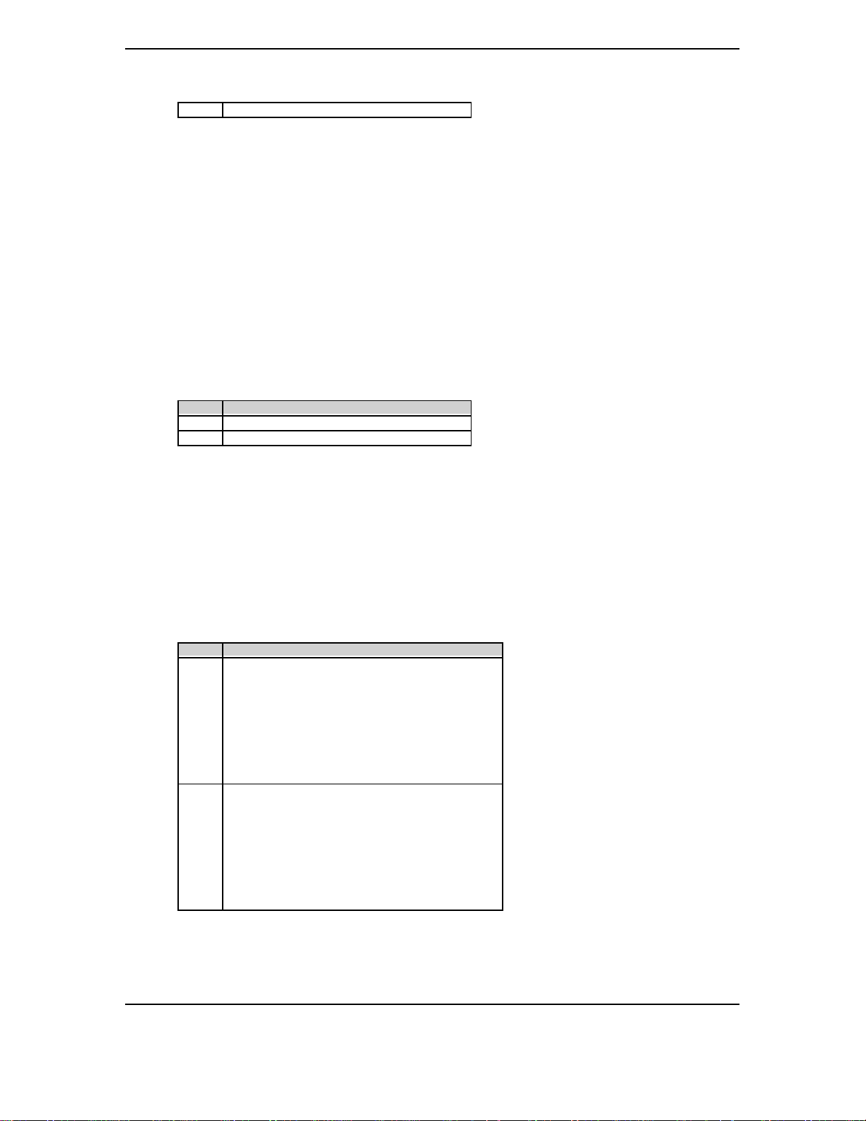
Chapter 4 System Support
6..0 Reserved
Configuration Byte 0Eh, Diagnostic Status
Default Value = 00h
This byte contains diagnostic status data.
Configuration Byt e 0 Fh, Sy stem Reset Code
Default Value = 00h
This byte contains the system reset code.
Configuration Byte 10h, Diskette Drive Type
Bit Function
7..4 Primary (Drive A) Diskette Drive Type
3..0 Secondary (Drive B) Diskette Drive Type
Valid values for bits <7..4> and bits <3..0>:
0010 = 1.2-MB drive
0011 = 720-KB drive
0110 = 2.88-MB drive
(all other values reserved)
0000 = Not installed
0001 = 360-KB drive
0100 = 1.44-MB/1.25-MB drive
Configuration Byte 12h, Hard Drive Type
Bit Function
7..4 Primary Controller 1, Hard Drive 1 Type:
0000 = none 1000 = Type 8
0001 = Type 1 1001 = Type 9
0010 = Type 2 1010 = Type 10
0011 = Type 3 1011 = Type 11
0100 = Type 4 1100 = Type 12
0101 = Type 5 1101 = Type 13
0110 = Type 6 1110 = Type 14
0111 = Type 7 1111 = other (use bytes 19h)
3..0 Primary Controller 1, Hard Drive 2 Type:
0000 = none 1000 = Type 8
0001 = Type 1 1001 = Type 9
0010 = Type 2 1010 = Type 10
0011 = Type 3 1011 = Type 11
0100 = Type 4 1100 = Type 12
0101 = Type 5 1101 = Type 13
0110 = Type 6 1110 = Type 14
0111 = Type 7 1111 = other (use bytes 1Ah)
Compaq Deskpro EN Series of Personal Computers
4-32
Desktop and Minitower Form Factors
Third Edi tion - September 1998
Page 82

Configuration Byte 13h, Security Functions
Default Value = 00h
Bit Function
7 Reserved
6 QuickBlank Enable After Standby:
0 = Disable
1 = Enable
5 Administrator Password:
0 = Not present
1 = Present
4 Reserved
3 Diskette Boot Enable:
0 = Enable
1 = Disable
2 QuickLock Enable:
0 = Disable
1 = Enable
1 Network Server Mode/Security Lock Override:
0 = Disable
1 = Enable
0 Password State (Set by BIOS at Power-up)
0 = Not set
1 = Set
Technical Reference Guide
Configuration Byte 14h, Equipment Installed
Default Value (standard configuration) = 03h
Bit Function
7,6 No. of Diskette Drives Installed:
00 = 1 drive 10 = 3 drives
01 = 2 drives 11 = 4 drives
5..2 Reserved
1 Coprocessor Present
0 = Coprocessor not installed
1 = Coprocessor installed
0 Diskette Drives Present
0 = No diskette drives installed
1 = Diskette drive(s) installed
Configuration Bytes 15h and 16h, Base Memory Size
Default Value = 280h
Bytes 15h and 16h hold a 16-bit value that specifies the base memory size in 1-KB (1024)
increments. Valid base memory sizes are 512 and 640 kilobytes .
Configuration Bytes 17h and 18h, Extended Memory Size
Bytes 17h and 18h hold a 16-bit value that specifies the extended memory size in 1-KB
increments.
Compaq Deskpro EN Series of Personal Computers
Desktop and Minitower Form Factors
Third Edi tion - September 1998
4-33
Page 83

Chapter 4 System Support
Configuration Bytes 19h-1Ch, Hard Drive Types
Byte 19h contains the hard drive type for drive 1 of the primary controller if byte 12h bits <7..4>
hold 1111b. Byte 1Ah contains the hard drive type for drive 2 of the primary controller if byte
12h bits <3..0> hold 1111b. Bytes1Bh and 1Ch contain the hard dr ive types for hard drives 1 and
2 of the secondary controller.
Configuration Byt e 1 Dh, Enhanced IDE H ard Drive Support
Default Value = F0h
Bit Function
7 EIDE - Drive C (83h)
6 EIDE - Drive D (82h)
5 EIDE - Drive E (81h)
4 EIDE - Drive F (80h)
3..0 Reserved
Values for bits <7..4> :
0 = Disable
1 = Enable for auto-configure
Configuration Byte 1Fh, Power Management Functions
Default Value = 00h
Bit Function
7..4 Reserved
3 Slow Processor Clock for Low Power Mode
0 = Processor runs at full speed
1 = Processor runs at slow speed
2 Reserved
1 Monitor Off Mode
0 = Turn monitor power off after 45 minutes in standby
1 = Leave monitor power on
0 Energy Saver Mode Indicator (Blinking LED)
0 = Disable
1 = Enable
Configuration Byt e 2 4 h, Sy st e m B oar d Ide nt i f i cation
Default Value = 7Eh
Configuration memory location 24h holds the system board ID.
Configuration Byte 25h, System Architecture Data
Default Value = 0Bh
Bit Function
7..4 Reserved
3 Unmapping of ROM:
0 = Allowed
1 = Not allowed
2 Reserved
1,0 Diagnostic Status Byte Address
00 = Memory locations 80C00000h-80C00004h
01 = I/O ports 878h-87Ch
11 = neither place
Compaq Deskpro EN Series of Personal Computers
4-34
Desktop and Minitower Form Factors
Third Edi tion - September 1998
Page 84

Configuration Byte 26h, Auxiliary Peripheral Configuration
Default Value = 00h
Bit Function
7,6 I/O Delay Select
00 = 420 ns (default)
01 = 300 ns
10 = 2600 ns
11 = 540 ns
5 Alternative A20 Switching
0 = Disable port 92 mode
1 = Enable port 92 mode
4 Bi-directional Print Port Mode
0 = Disabled
1 = Enabled
3 Graphics Type
0 = Color
1 = Monochrome
2 Hard Drive Primary/Secondary Address Select:
0 = Primary
1 = Secondary
1 Diskette I/O Port
0 = Primary
1 = Secondary
0 Diskette I/O Port Enable
0 = Primary
1 = Secondary
Technical Reference Guide
Configuration Byte 27h, Speed Control/External Drive
Default Value = 00h
Bit Function
7 Boot Speed
0 = Max MHz
1 = Fast speed
6..0 Reserved
Configuration Byte 28h, Expanded and Base Memory, IRQ12 Select
Default Value = 00h
Bit Function
7 IRQ12 Select
0 = Mouse
1 = Expansion bus
6,5 Base Memory Size:
00 = 640 KB
01 = 512 KB
10 = 256 KB
11 = Invalid
4..0 Internal Compaq Memory:
00000 = None
00001 = 512 KB
00010 = 1 MB
00011 = 1.5 MB
.
.
11111 = 15.5 MB
Compaq Deskpro EN Series of Personal Computers
Desktop and Minitower Form Factors
Third Edi tion - September 1998
4-35
Page 85

Chapter 4 System Support
Configuration Byte 29h, Miscellaneous Configuration Data
Default Value = 00h
Bit Function
7..5 Reserved
4 Primary Hard Drive Enable (Non-PCI IDE Controllers)
0 = Disable
1 = Enable
3..0 Reserved
Configuration Byte 2Ah, Hard Drive Timeout
Default Value = 02h
Bit Function
7..5 Reserved
4..0 Hard Drive Timeout
00000 = Disabled
00001 = 1 minute
00010 = 2 minutes
.
.
10101 = 21 minutes
Configuration Byte 2Bh, System Inactivity Timeout
Default Value = 23h
Bit Function
7 Reserved
6,5 Power Conservation Boot
00 = Reserved
01 = PC on
10 = PC off
11 = Reserved
4..0 System Inactive Timeout. (Index to SIT system timeout record)
00000 = Disabled
Configuration Byte 2Ch, ScreenSave and NUMLOCK Control
Default Value = 00h
Bit Function
7 Reserved
6 Numlock Control
0 = Numlock off at power on
1 = Numlock on at power on
5 Screen Blank Control:
0 = No screen blank
1 = Screen blank w/QuickLock
4..0 ScreenSave Timeout. (Index to SIT monitor timeout record)
000000 = Disabled
Compaq Deskpro EN Series of Personal Computers
4-36
Desktop and Minitower Form Factors
Third Edi tion - September 1998
Page 86

Configuration Byt e 2 Dh, Additional Flag s
Default Value = 00h
Bit Function
7..5 Reserved
4 Memory Test
0 = Test memory on power up only
1 = Test memory on warm boot
3 POST Error Handling (BIOS Defined)
0 = Display “Press F1 to Continue” on error
1 = Skip F1 message
2..0 Reserved
Configuration Byte 2Eh, 2Fh, Checksum
These bytes hold the checksum of bytes 10h to 2Dh.
Configuration Byte 30h, 31h, Total Extended Memory Tested
Technical Reference Guide
This location holds the amount of system memory that checked good during the POST.
Configuration Byte 32h, Century
This location holds the Century value in a binary coded decimal (BCD) format.
Configuration Byte 33h, Miscellaneous Flags
Default Value = 80h
Bit Function
7 Memory Above 640 KB
0 = No, 1 = Yes
6 Reserved
5 Weitek Numeric Coprocessor Present:
0 = Not installed, 1 = Installed
4 Standard Numeric Coprocessor Present:
0 = Not installed, 1 = Installed
3..0 Reserved
Configuration Byte 34h, International Language Support
Default Value = 00h
Compaq Deskpro EN Series of Personal Computers
Desktop and Minitower Form Factors
Third Edi tion - September 1998
4-37
Page 87

Chapter 4 System Support
Configuration Byte 35h, APM Status Flags
Default Value = 11h
Bit Function
7..6 Power Conservation State:
00 = Ready
01 = Standby
10 = Suspend
11 = Off
5,4 Reserved
3 32-bit Connection:
0 = Disconnected, 1 = Connected
2 16-bit Connection
0 = Disconnected, 1 = Connected
1 Real Mode Connection
0 = Disconnected, 1 = Connected
0 Power Management Enable:
0 = Disabled
1 = Enabled
Configuration Byt e 3 6 h, E CC PO ST T e st Si ng l e Bit Er rors
Default Value = 01h
Bit Function
7 Row 7 Error Detect
6 Row 6 Error Detect
5 Row 5 Error Detect
4 Row 4 Error Detect
3 Row 3 Error Detect
2 Row 2 Error Detect
1 Row 1 Error Detect
0 Row 0 Error Detect
0 = No single bit error detected.
1 = Single bit error detected.
Configuration Byt e 3 7 h-3 Fh, Power -On Password
These eight locations hold the power-on password.
Configuration Byte 40h, Miscellaneous Disk Data
Configuration Bytes 41h-44h, Hood Removal Time Stamp
These four bytes record the time at which the hood of the system was removed:
Byte 41h, month & day
Byte 42h, year and month
Byte 43h, min utes an d seconds
Byte 44h, removal flag and minutes
Compaq Deskpro EN Series of Personal Computers
4-38
Desktop and Minitower Form Factors
Third Edi tion - September 1998
Page 88

Configuration Byte 45h, Keyboard Snoop Data
Default Value = xxh
Bit Function
7 Cntrl/F10 Key Status:
0 = Cntrl & F10 keys not pressed
1 = Cntrl & F10 keys pressed
6 F10 Key Status:
0 = F10 key not pressed
1 = F10 key pressed
5..1 Reserved
0 Key Pressed Flag:
0 = Key not pressed
1 = Key pressed
Configuration Byte 46h, Diskette/Hard Drive Status
Default Value = xxh
Bit Function
7,6 Reserved
5 Partition On HD:
0 = Not set, 1 = Set
4 Setup Disk:
0 = Not present, 1 = Present
3 ROMPAQ or DIAGS Diskette:
0 = Not present, 1 = Present
2 Boot Diskette in Drive A:
0 = No, 1 = Yes
1 Drive B: Present:
0 = Not present, 1 = Present
0 Drive A: Present:
0 = Not present, 1 = Present
Technical Reference Guide
Configuration Bytes 47h-4Fh, IPL Data
These bytes hold initial program load (IPL) data for boot pu rpos es:
Byte 47h, last IPL device
Bytes 48h-4Bh, IPL priority
Byte 4Ch-4Fh, BCV priority
Configuration Byte 51h, ECC Status Byte
Default Value = xxh
Bit Function
7 ECC Status for DIMM 3
6 ECC Status for DIMM 2
5 ECC Status for DIMM 1
4 ECC Status for DIMM 0
3..0 Reserved
Compaq Deskpro EN Series of Personal Computers
Desktop and Minitower Form Factors
4-39
Third Edi tion - September 1998
Page 89

Chapter 4 System Support
Configuration Byte 52h, Board Revision
This byte holds the board revis ion as copied from t he boot block se ctor.
Configuration Byte 53h, 54h, SW SMI Command/Data Bytes
Configuration Byte 55h, APM Command Byte
Configuration Byte 56h, Miscellaneous Flags Byte
Bit Function
7 CAS Latency:
0 = 2, 1 = 3
6 IR Port Enable Flag:
0 = Disabled (COM2 config. for standard serial port)
1 = Enabled (COM2 config. for IrDA)
5 Warm Boot Enable Flag:
0 = Disable, 1 = Enable
4 POST Terse/Verbose Mode
0 = Verbose, 1 = Terse
3..1 Erase Ease Keyboard Mode:
000 = Backspace/Spacebar
001 = Spacebar/Backspace
010 = Spacebar/Spacebar
011-111 = Invalid
0 Configurable Power Supply:
0 = Power switch active
1 = Power switch inhibited
Configuration Byte 57h-76h, CMOS Copy
Configuration Byt e s 7 7 h-7 Fh, Admini st r a t or Password
Configuration Byte 80h, CMOS Diagnostic Flags Byte
Default Value = 00h. Set bit indicates function is valid.
Bit Function
7 CMOS Initialization (Set CMOS to Default)
6 Setup password locked
5 PnP should not reject SETs because Diags is active
4 Reserved
3 Manufacturing diagnostics diskette found
2 Invalid electronic serial number
1 Boot maintenance partition once
0 I nvalid CMOS checksum
Configuration Byte 81h, 82h, Total Super Extended Memory Tested
This byte holds the value of the amount of extended system memory that tested good during
POST. The am oun t is gi ven in 64-KB increment s.
Compaq Deskpro EN Series of Personal Computers
4-40
Desktop and Minitower Form Factors
Third Edi tion - September 1998
Page 90

Technical Reference Guide
Configuration Byte 83h, Microprocessor Identification
This byte holds the component ID and chip revision of the microprocessor.
Configuration Byte 84h, Microprocessor Revision
Configuration Byte 85h, Administration Mode
Bit Function
7,6 Reserved
5 ESCD Bufferi ng:
0 = No buffering, 1 = ESCD buffered at F000h.
4 Hood Lock Enable:
0 = Disabled, 1 = Enabled
3 User Mode Flag
2 Administration Mode Flag
1 Level Support:
0 = Level 1, 1 = Level 2
0 Feature Support Bit
0 = Disabled, 1 = Enabled
Configuration Byte 86h, Fast Boot Date
Configuration Byte 87h, Fast Boot Select
Bit Function
7..3
2
1
0
Configuration Byte 88h, Fast Boot Date (Year/Century)
Configuration Byte 89h, APM Resume Timer
Bit <7> indicates the timer status: 0 = disabled, 1 = timer set.
Configuration Byt e 8 Ah- 8Fh, APM Re sume Timer
These bytes hold th e APM timer values:
Byte 8Ah, minutes
Byte 8Bh, hours
Byte 8Ch, day
Byte 8Dh, month
Byte 8Eh, year
Byte 8Fh, century
Compaq Deskpro EN Series of Personal Computers
Desktop and Minitower Form Factors
Third Edi tion - September 1998
4-41
Page 91

Chapter 4 System Support
Configuration Byte 90h, 91h, Total Super Extended Memory Configured
This byte holds the value of the amount of extended system memory that is configured.
The amount is given in 64-KB incr ement s.
Configuration Byte 92h, Miscellaneous Configuration Byte
Default Value = 18h
Bit Function
7..5 Reserved
4 Diskette Write Control:
0 = Disable
1 = Enable
3..1 Reserved
0 Diskette Drive Swap Control:
0 = Don’t swap
1 = Swap drive A: and B:
Configuration Byte 93h, PCI Configuration Byte
Default Value = 00h
Bit Function
7 Onboard SCSI Status:
0 = Hidden
1 = Active
6 Onboard NIC Status:
0 = Hidden
1 = Active
5 Onboard USB Status:
0 = Hidden
1 = Active
3 Reserved
2 ISA Passive Release:
0 = Enabled
1 = Disabled
1 PCI Bus Master Enable
0 = Enabled
1 = Disabled
0 PCI VGA Palette Snoop
0 = Disable
1 = Enable
If palette snooping is enabled, then a primary PCI graphics card may share a common palette
with the ISA graphics card. Palette snooping should only be enabled if all of the following
conditions are met:
♦
An IS A card connect s to a PCI g raphics card through the VESA connect or.
♦
The ISA card is connected to a color monitor.
♦
The ISA card uses the RAMDAC on t he PCI card
♦
The palette snooping feature (sometimes called “RAMDAC shadowing ” ) on the PCI card is
enabled and functioning properly.
Compaq Deskpro EN Series of Personal Computers
4-42
Desktop and Minitower Form Factors
Third Edi tion - September 1998
Page 92

Configuration Byte 94h, ROM Flash/Power Button Status
Default Value = 00h
Bit Function
7..5 Reserved
4 ROM Flash In Progress (if set)
3 Reserved
2 Power Button Inhibited (if set)
1 User-Forced Bootblock (if set)
0 ROM Flash In Progress (if set)
Configuration Byt e 9 7 h, Asset/Test Prompt B yt e
Default Value = 00h
Bit Function
7,6 Test Prompt:
01 = Fake F1
10 = Fake F2
11 = Fake F10
5..0 Asset Value
Configuration Byte 9Bh, Ultra-33 DMA Enable B yte
Default Value = 00h
Bit Function
7..4 Reserved
3 Secondary Slave Enabled for U-33 if Set
2 Secondary Master Enabled for U-33 if Set
1 Primary Slave Enabled for U-33 if Set
0 Primary Master Enabled for U-33 if Set
Technical Reference Guide
Configuration Byte 9Ch, Mode-2 Configuration Byte
Default Value = 1Ch
Bit Function
7,6 Reserved
5 Mode 2 Support
0 = Disable
1 = Enable
4 Secondary Hard Drive Controller
0 = Disable
1 = Enable
3,2 Secondary Hard Drive Controller IRQ
00 = IRQ10
01 = IRQ11
10 = IRQ12
11 = IRQ15
1,0 Reserved
Compaq Deskpro EN Series of Personal Computers
Desktop and Minitower Form Factors
Third Edi tion - September 1998
4-43
Page 93

Chapter 4 System Support
Configuration Byt e 9 Dh, ESS Audio Configuration Byte
Default Value = 12h
Bit Function
7 Reserved for Game Port Enable
6,5 Audio Address
00 = 22xh
01 = 23xh
10 = 24xh
11 = 25xh
4,3 DMA Channel
00 = Disabled
01 = DMA0
10 = DMA1
11 = DMA3
2,1 IRQ Select
00 = IRQ9
01 = IRQ5
10 = IRQ7
11 = IRQ10
0 ESS Audio Chip Enable
0 = Enabled
1 = Disabled
Configuration Byte 9Eh, ECP DMA Configuration Byte
Default Value = 03h
Bit Function
7..4 Reserved
3 SafeStart Control:
0 = Disable
1 = Enable
2..0 ECP DMA Channel
000 = Invalid
100 = Disabled
All other values (001-011, 101-111) refer to channel no.
Configuration Byte 9Fh-AFh, Asset Tag Serial Number
Configuration Byt e s B0h-C3h; Custom Hard Dri ve Informat i on
These bytes contain the number of cylinders, heads, and sectors per track for hard drives C, D, E,
and F respectively. The mapping for each drive is as follows:
Drive 65 (C) Drive 66 (D) Drive 68 (E) Drive 15 (F) Function
B0h B5h BAh BFh No. of Cylinders, Low Byte
B1h B6h BBh C0h No. of Cylinders, High Byte
B2h B7h BCh C1h No. of Heads
B3h B8h BDh C2h Max ECC Bytes
B4h B9h BEh C3h No. of Sectors Per Track
Compaq Deskpro EN Series of Personal Computers
4-44
Desktop and Minitower Form Factors
Third Edi tion - September 1998
Page 94

Technical Reference Guide
Configuration Byte C7h, C8h, Serial Ports 1 and 2 (Respectively) Configuration Bytes
Default Value = FEh, 7Dh
Bit Function
7..2 Base I/O Address (in packed format)
(Algorithm: [Addr. - 200h] / 8)
(i.e., 3Fh = 3F8h, 1Fh = 2F8h, 00 = 200h)
1..0 Interrupt:
00 = Reserved
01 = IRQ3
10 = IRQ4
11 = Reserved
Configuration Byt e s CAh, DBh; Chassis Serial Number
Configuration Byt e s DE h, DFh; Checksum of Locations 90h-DDh
Configuration Bytes E0h-FFh; Client Management Error Log
Compaq Deskpro EN Series of Personal Computers
Desktop and Minitower Form Factors
Third Edi tion - September 1998
4-45
Page 95

Chapter 4 System Support
4.7 I/O MAP AND REGISTER ACCESSING
4.7.1 SYSTEM I/O MAP
Table 4–19.
System I/O Map
Table 4-19.
System I/O Map
I/O Port Function
0000..000Fh DMA Controller 1
0020..0021h Interrupt Controller 1
0040..0043h Timer 1
0060h Keyboard Controller Data Byte
0061h NMI, Speaker Control
0064h Keyboard Controller Command/Status Byte
0070h NMI Enable, RTC/Lower CMOS Index
0071h RTC Data
0078h-007Bh GPIO Port 1 Control (87307 I/O controller)
007Ch-007Fh GPIO Port 2 Control (87307 I/O controller)
0080..008Fh DMA Page Registers
0092h Port A, Fast A20/Reset
00A0..00A1h Interrupt Controller 2
00B2h, 00B3h APM Control/Status Ports
00C0..00DFh DMA Controller 2
00F0h Math Coprocessor Busy Clear
015C, 015Dh 87307 I/O Controller Configuration Registers (Index, Data)
0170..0177h Hard Drive (IDE) Controller 2
01F0..01FFh Hard Drive (IDE) Controller 1
0201..024Fh Audio subsystem control (primary & secondary addresses)
0278..027Bh Parallel Port (LPT2)
02F8..02FFh Serial Port (COM2)
0371.. 0375h Diskette Drive Controller Alternate Addresses
0376h IDE Controller Alternate Address
0377h IDE Controller Alternate Address, Diskette Drive Controller Alternate Address
0378..037Fh Parallel Port (LPT1)
0388..038Bh FM synthesizer (alias addresses)
03B0..03DFh Graphics Controller
03E8..03EFh Serial Port (COM3)
03F0..03F5h Diskette Drive Controller Primary Addresses
03F6, 03F7h Diskette Drive Controller Primary Addresses, Hard Drive Controller Primary Addresses
03F8..03FFh Serial Port (COM1)
04D0, 04D1h Master, Slave Edge/Level INTR Control Register
0C00, 0C01h PCI IRQ Mapping Index, Data
0C06, 0C07h Reserved - Compaq proprietary use only
0C50, 0C51h System Management Configuration Registers (Index, Data)
0C52h General Purpose Port
0C7Ch Machine ID
0CF8h PCI Configuration Address (dword access)
0CF9h Reset Control Register
0CFCh PCI Configuration Data (byte, word, or dword access)
FF00..FF07h IDE Bus Master Register
NOTE: Assume unmarked gaps are reserved/unused.
Compaq Deskpro EN Series of Personal Computers
4-46
Desktop and Minitower Form Factors
Third Edi tion - September 1998
Page 96

4.7.2 GPIO UTILIZATION
This section describes the utilization of general purpose input/output (GPIO) ports provided by
the south bridge (82371) and I/O controller (87307) components used in this system.
4.7.2.1 82371 South Bridge GPIO Utilization
The 82371 South Bridge component includes a number of single and dual purpose pins available
as gener a l purpose input/outpu t ( GPI O) p or ts. Th e GPIO ports are config u red duri ng POST by
BIOS through the PCI configuration registers B0-B3h (82371, function 0). The GPI ports are
monitored through registers of the Power Management function (function 3) at I/O address PM
base +30h. The GPO ports are controlled through a register of functi on 3 at I/O address PM base
+34h.
Tables 4-20 and 4-21 list the utilization of the GPI and GPO ports r especti vely in t his system.
Technical Reference Guide
Table 4–20.
82371 South Bridge General Purpose Input Port Utilization
Table 4-20.
82371 South Bridge General P ur pos e Input Port Utiliz ation
GP Input Port Function
GPI #0 IOCHK- function for ISA bus.
GPI #1 SCI- event status.
GPI #2..5 Not used.
GPI #6 Interrupt (IRQ8) for RTC (in 87307 I/O controller).
GPI #7 Not used.
GPI #8 Magic packet SMI event status. When read low, magic packet has occurred.
GPI #9 Not used.
GPI #10 Wakeup w/ IRQ12. Will, in S1 state, be high if an IRQ12 (mouse interrupt) occurred.
GPI #11 Not used
GPI #12 Wake up w/ IRQ1. Will, in S1 state, be high if an IRQ1 (keyboard interrupt) occurred.
GPI #13 PME status.
GPI #14, 15 Backplane revision bits <0, 1>
GPI #16 Not used.
GPI #17 Primary IDE cable type: 0 = 80-pin cable attached, 1 = 40-pin cable attached.
GPI #18 Secondary IDE cable type: 0 = 80-pin cable attached, 1 = 40-pin cable attached.
GPI #19 Chassis fan status: 0 = fan not connected, 1 = fan connected.
GPI #20 Processor thermal caution status: 0 = not occurred, 1 = occurred.
GPI #21 Themal sensor: 0 = diode connected, 1 = diode not connected.
Compaq Deskpro EN Series of Personal Computers
Desktop and Minitower Form Factors
Third Edi tion - September 1998
4-47
Page 97

Chapter 4 System Support
Table 4–21. 82371 South Bridge General Purpose Output Port Utilization
82371 South Bridge General P ur pos e Output Port Utilization
GP Output Port Function
GPO #0 PCI reset. When low will generate a PCI RST- to PCI slots.
GPO #1-7 ISA bus address signals LA17-23.
GPO #8 Not used.
GPO #9 Not used.
GPO #10 Not used.
GPO #11 Not used.
GPO #12 Not used.
GPO #13 Not used.
GPO #14 Not used
GPO #15 Not used.
GPO #16 Power management suspend control signal.
GPO #17 CPU clock stop. When cleared inhibits the clock generator from producing CPU clock.
GPO #18 PCI clock stop. When cleared inhibits the clock generator from producing PCI clock.
GPO #19 Not used.
GPO #20 Power management suspend control signal.
GPO #21 Not used.
GPO #22, 23 X-bus control signals.
GPO #24 Not used.
GPO #25 Not used.
GPO #26 Not used.
GPO #27 Chassis fan control. When cleared (0) shuts down the chassis fan.
GPO #28-30 Not used.
Table 4-21.
Compaq Deskpro EN Series of Personal Computers
4-48
Desktop and Minitower Form Factors
Third Edi tion - September 1998
Page 98

4.7.2.2 87307 I/O Controller Functions
The 87307 I/O controller contains various functions such as the keyboard/mouse interfaces,
diskette interface, serial interfaces, and parallel interface. While the control of these interfaces
uses standard AT-type I/O addressing, the configuration of these functions uses indexed ports
unique to the 87307. In this system, hardware strapping selects I/O addresses 015Ch and 015Dh
at reset as the Index/Data ports for accessing the logical devices within the 87307. The hardware
strapping a l so places the 87307 into PnP mother board mode. The in tegr a t ed logical devices are
listed as follows:
Table 4-22 lists the PnP standard control registers for the 87307.
Technical Reference Guide
Table 4–22.
87307 I/O Controller PnP Stan da rd Control Registers
Table 4-22.
87307 I/O Controller PnP Standard Cont r ol Regis ters
Index Function Reset Value
00h Set RD_DATA Port 00h
01h Serial Isolation
02h Configuration Control
03h Wake (CSN) 00h
04h Resource Data
05h Status
06h Card Select Number (CSN) 00h
07h Logical Device Select:
00h = 8042 Controller (Keyboard I/F)
01h = 8042 Controller (Mouse I/F)
02h = RTC/APC Configuration
03h = Diskette Controller
04h = Parallel Port
05h = UART 2 (Serial Port B / IrDA)
06h = UART 1 (Serial Port A)
07h = GPIO Ports
08h = Power Management
20h Super I/O ID Register (SID) A0h
21h SIO Configuration 1 Register 16h
22h SIO Configuration 1 Register 02h
23h Programmable Chip Select Configuration Index 00h
24h Programmable Chip Select Configuration Data 00h
NOTE:
For a detailed description of registers refer to appropriate National documentation.
00h
The configuration registers are accessed by writing the appropriate logical device’s number to
index 07h and writing the desired offset to the index register. The data is then either written to or
read from the data register.
Compaq Deskpro EN Series of Personal Computers
Desktop and Minitower Form Factors
Third Edi tion - September 1998
4-49
Page 99

Chapter 4 System Support
87307 GPIO Utilization
The 87307 I/O Controller provides 11 general purpose pins that can be individually configured as
either inputs or outputs. These pins are mapped as two general purpose ports and utilized as
shown below.
GPIO Port 1 Data, I/O Addr. 078h, (87307 I/O Controller),
Bit Function
7 GPIO17 (not used)
6 GPIO16 (config. as input): Cover Lock Detect.
Read 0, no solenoid
Read 1, solenoid
5 GPIO15 (config. as output): Cover Alarm Clear.
Write 0 to clear alarm.
4 GPIO14 (config. as input): Cover Removed Detect.
Read 0, cover has been removed
Read 1, cover is secure
3..0 GPIO13-10 (config. as input):
Backplane identification (BP_ID3-0)
GPIO Port 1 Direction/Output Type/PU Cntrl., I/O Addr. 079-07Bh, (87307 I/O
Controller)
GPIO Port 2 Data, I/O Addr. 07Ch, (87307 I/O Controller),
Bit Function
7..4 GPIO27..24 Not Available
3 GPIO23 (config. as input): Ring Detect
Read 0, no ring received
Write 1, ring detected
2..0 GPIO22..20 Not Available
GPIO Port 2 Direction/Output Type/PU Cntrl., I/O Addr. 07D-07Fh, (87307 I/O
Controller)
Compaq Deskpro EN Series of Personal Computers
4-50
Desktop and Minitower Form Factors
Third Edi tion - September 1998
Page 100

4.8 SYSTEM MANAGEMENT SUPPORT
This section describes the hardware support of functions involving security, safety, identification,
and power consumption of the system. System management functions are handled largely by a
System Security ASIC. Most functions are controlled through registers (Table 4-23) accessed
using the indexed method through I/O ports 0C50h (index) and 0C51h (Data).
Technical Reference Guide
Table 4–23.
System Management Control Registers
Table 4-23.
System Management Control Registers
Index Function
00h Identification
02h Temperature Status / Clear
03h Temperature Interrupt / SMI Enable
05h Power On LED Blink Control
12h General Purpose Open Collector (GPOC) Bits
13h Secured GPOC Bits
20h Power Button Control
21h SMI / SCI Source
22h SMI / SCI Mapping
30h REQ/GNT Control
80h Super I/O Security Control
81h Super I/O Index Address Low
82h Super I/O Index Address High
83h Super I/O Index Data
84h Super I/O Data Address Low
85h Super I/O Data Address High
86h Super I/O Write Block 0
87h Super I/O Write Block 1
88h Super I/O Write Block 2
89h Super I/O Write Block 3
The following subsections describe the system management functions. Any BIOS interaction
required of these functions is described in Chapter 8, “BIOS” or in the Compaq BIOS Technical
Reference G u ide.
Compaq Deskpro EN Series of Personal Computers
Desktop and Minitower Form Factors
Third Edi tion - September 1998
4-51
 Loading...