

Page 1
Xiamen Clarion Electrical Enterprise Co., Ltd
8/F., Xiamen Mail Processing Centre, No.275 Lujiang Road, Xiamen, China
Tel:+86-592-2389080 Fax:+86-592-2389089
Clarion Co., Ltd.
50 Kamitoda, Toda-shi, Saitama 335-8511 Japan
Service Manual
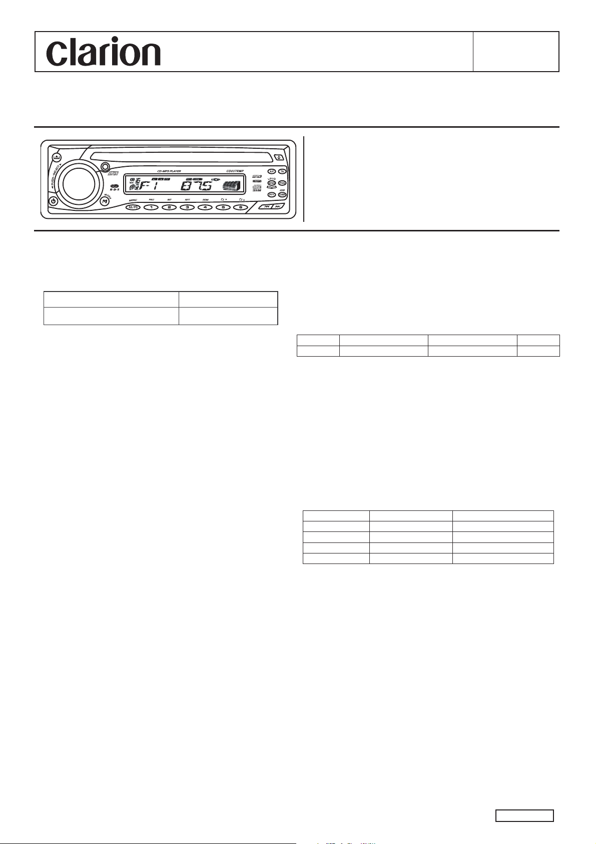
CD/USB/MP3 Receiver
Published by Service Dept.
298-6400-37-02 (GEN. 2009)
Printed in P.R.C.
ORIGINAL SERVICE MANUAL
This additional service manual is designed to be used
together with Original Model CD037RMP
Original Model Manual No.
CD037RMP
298-6400-37-00
DIFFERENCE FROM ORIGINAL
MODEL
1. EXPLANATION OF IC
2. PART LIST
Switch DCP Section
Main Section
3. ELETRICAL PARTS LIST
Main PWB Section
4. PRINTED WIRING BOARD
Section CD MECHANISM
5. PRINTED WIRING BOARD
Main PWB section
6. CIRCUIT DIAGRAM
Section CD MECHANISM
Model
CD037RMP
DIFFERENCE
EXPLODE VIEW .PART LIST
Switch DCP Section/Main Section
(Refer to page 10 of the original
service manual)
NO.
29
PARTS NO.
SERVOCD037V2
DESCRIPTION
SERVO PCB
DIFFERENCE
ELETRICAL PARTS LIST
Main PWB Section
(Refer page 11 to 14 of the original
service manual)
REF. No.
IC201
LED202
CON1
CON1
PART. No.
0010RF881703100
017WWOR150TSC00
377R140125B0000
37814125120MU00
Description
MCU RF8817-031
LED Red
FPC/FFC Connector 14
FFC 14 pin
Q’TY
1
7. CIRCUIT DIAGRAM
Main PWB Section
NOTE
* Specifi cations and design are subject to change without notice
for further improvement.
-1-
CD037RMP
Page 2

EXPLANATION IC
PIN FUNCTION
DOCUMENT No: RF8817-0x1
PIN P-NAME I/O Act DESCRIPTION When not Used REMARK
1 BT_OUT
DIO IN4 O I
2 IPOD_O
DIO IN3 O I
3 DIOO3 O H Optional diode output 3
4 DIOO2 O H Optional diode output 2
5 DIOO1 O H Optional diode output 1
6 RESET HD L To start u-COM,
7 3 COLOR
/DIO IN2
8 2 COLOR
/ALARM
/DIO IN1
H Bluetooth Audio Control Output.
Option diode input 4.
H iPod Audio Control output.
Option diode input 3.
High input should be triggered with high input.
3.2V reset is recommendable.
O H 1. 3 COLOR output for front illumination.
2. Option diode input 2.
1. When front opened, the output is generated
per 1sec. with 10% duty (LOW=LED on).
With this port, a flashing LED is used.
2. When power is on, by pressing the {DISP}
key for more than 1sec. the output is toggled.
With this port, the switching of 2 color lamps can
be used.
3. Option diode input 1.
Open
Open
Refer to
the circuit
9 FLMD0 HD H This is a pin for setting flash memory programming
mode.
Connect FLMD0 to GND in the normal operation
mode.
In flash memory programming mode, connect this
pin to the flash programmer.
Series resister 4.7Kohm is needed to GND.
10 X-IN HD 7.2 MHz X-TAL INPUT
11 X-OUT HD 7.2 MHz X-TAL OUTPUT
12 REGC HD Regulated Voltage output Open
13 GND HD Ground.
14 GND HD Ground.
15 VDD HD VDD 5V DC
16 VDD HD VDD 5V DC
17 TOUCH_
DAT
18 TOUCH_
ALBEN
O Data in/out from/to Touch Sensor(DT8800)
Direct Connect with Pin50
I/O Control output to DT8800.
Direct Connect with Pin49
Open
DRAIN
Open
DRAIN
-2-
CD037RMP
Page 3

PIN P-NAME I/O Act DESCRIPTION When not Used REMARK
19 VR CLK O E.VR Communication CLK OUT
Needed pull up resistor(2.2K) from switch 5Vdc.
20 VR DATA O E.VR Communication DATA OUT
Needed pull up resistor(2.2K) from switch 5Vdc.
21 SD_DET
/DIO IN12
22 F_INH O H FRONT Communication INH output.
23 F_DATA I/O FRONT LCD driver Communication data.
24 F_CLK I/O FRONT and LED driver Communication clock.
25 F_CE O H Front Communication Chip Enable.
26 TEF_SCL
PLL_CLK
/STIN
27 TEF_SDA
PLL_CD
28 PLL_CE O PLL IC Communication CHIP ENABLE
29 LOCAL O H Radio LOCAL output during seek(Loc=High)
30 CDPRST O L Reset the DSP and ASP in CDP. Open
I L 1. SD Detection Input.
2. Option diode input 12.
I/O
O
I
I/O O 1.Data out/in to TEF6606 Tuner
1.Clock output to TEF6606 Tuner
2.PLL IC Communication CLOCK OUT.
3.ST input. Low=Stereo.
Series 2.2Kohm to STIN must be added.
2.PLL IC Communication DATA INPUT/OUTPUT
Open Open
Open Open
Pull up
DRAIN
DRAIN
31 CDPO O H At CDP mode H is output.
32 USB_DET I L USB Detection Input
33 REMOCON I Remote control input.
The power supply of Remote receiver is to be
turned off during ACC off.
34 SYSTEM
POWER
35 MUTEOUT O L Mute output for power IC(LOW=MUTE)
36 FEEDF O H FEED Motor Forward in single CDP. Open
37 FEEDR O H FEED Motor Reverse in single CDP. Open
38 CDC BUS
TOUCH_
CLK
39 RDS DATA I RDS Data Input in RDS Model. Pull up
O H When radio is power on (High=power on).
This port is to control power on of the system.
I/O CD CHANGER Communication BUS Input
Pull down resistor(1M) should be connected.
A zener diode (5.6V) to GND is recommendable
to protect from a outside surge.
Add series 220ohm to protect port.
Clock in/out from/to Touch Sensor(DT8800)
Pull Down
1M
Pull
Down
Pull Down
1M
40 {RDS CLK} I/O H RDS Clock Input GND Pull Down
1M
-3-
CD037RMP
Page 4

PIN P-NAME I/O Act DESCRIPTION When not Used REMARK
41 B_UP
42 BT_RXD I Bluetooth RXD Input.
43 BT_TXD O Bluetooth TXD output.
44 IPOD_DET I H IPOD detection input for connection input. Pull down 220k
45 NC I Reserved for future use. Pull up
46 AF MUTE O H RDS AF MUTE output.(High=Mute).
47 VDD HD VDD 5V DC.
48 GND HD Ground.
49 KEYADI2 I AD KEY INPUT2.
50 KEYADI1
/FRT DET
51 DANCE3 I Level dancing input3 (ex: 10kHz) GND AD input
52 DANCE2 I Level dancing input2 (ex: 1kHz) GND AD input
I L 1. ACC ON Detection input. (Low=system halt).
To detect rapidly, standard circuit is
recommendable
described in hardware application note.
Must be pulled up with 4.7Kohm from AVREF
in MAIN PCB.
I Key A/D input1 and front detect input.
Must be pulled down with 1Mohm in main PCB.
Must be pulled up with 4.7Kohm from AVREF
in front PCB.
Refer to
the circuit
AD input
AD input
53 DANCE1 I Level dancing input1 (ex: 100Hz) GND AD input
54 S-METER I Connected to S-METER output of IF ICs. AD input
55 TEL/CDSW I 1. TELPHONE MUTE INPUT(4.54~5.0 Vdc)
2. S-cdp switch input.
Must be pulled up with 47Kohm from AVREF.
Must be pulled down with 330Kohm to AGND.
56 ENCODER I Encoder volume input.
Pull up 47Kohm from AVREF and Pull-down
330Khom to GND.
Series 82Kohm to VOL B.
Series 47Kohm to VOL A/C.
57 SAT_PW
DIO IN11
58 MP3_CK
/DIO IN10
59 MP3_DI I MP3 Communication data output.
60 MP3_DO
/DIO IN9
I H 1. High output in XM mode for XM power.
2.Option diode input 11.
O 1. MP3 Communication CLK output.
2. Option diode input 10.
Needed pull up 220ohm from CDP powered 5V.
O 1. S-CDP/MP3 Communication data output.
2. Option diode input 9.
AD input
GND Refer to
the circuit
-4-
CD037RMP
Page 5

PIN P-NAME I/O Act DESCRIPTION When not Used REMARK
61 MONO
/AUX OUT
/DIO IN8
62 MP3_REQ
/DIO IN7
63 BEEP
/FUNC
/DIO IN6
64 SENS1_O
/DIO IN5
O H 1. Forced mono control output (High=mono).
2. AUX output (High = AUX mode).
3. Option diode input 8.
I L 1. MP3 request input from MP3 module.
2. Option Diode input7.
O 1. BEEP SOUND OUTPUT
It should be connected with the normal audio
signal.
Unless special requirement, it is recommended to
be
connected to front CH of audio signal.
2. FUNC OUT (FUNC=HIGH)
3. Option diode input 6.
O H 1. For the optical loading S/W,
Connect to the Anode of loading sens LED of CDP
with TR for AUTO POWER ON
2. Option Diode input 5.
Open
-5-
CD037RMP
Page 6

DIFFERENCE
PRINTED WIRING BOARD
Section CD MECHANISM 1/2
-6-
CD037RMP
Page 7

DIFFERENCE
PRINTED WIRING BOARD
Section CD MECHANISM 2/2
-7-
CD037RMP
Page 8

CD037RMP
-8-
DIFFERENCE
PRINTED WIRING BOARD
Main PWB section 1/2
Page 9

CD037RMP
-9-
DIFFERENCE
PRINTED WIRING BOARD
Main PWB section 2/2
Page 10

CD037RMP
DIFFERENCE
CIRCUIT DIAGRAM
Section CD MECHANISM 1/1
-10-
Page 11

1234567891011 12 13 14 15 16 17 18 19 20
21 22
HCC
RDS RFAFL-OUT
R-OUTSDIF
MONO
AM OSC
GND
AGC
RA+
AM/LW
AM VT
AM+
AM LOC
FM LOC
FM+
GND
GND
FM OSC
FM VT
TUNER1
TUNER008
1
2
3
4
5
6
7
8
9
10
11
12
13
14
15
16
17 18 19 20 21 22 23 24 25 26 27 28 29 30 31 32
33
34
35
36
37
38
39
40
41
42
43
44
45
46
47
48
49505152535455565758596061626364
BT IN4)
(IPOD IN3)
DIO OUT3
DIO OUT2
DIO OUT1
RESET
3COLOR(DIO IN2)
(DIO IN1)
FLDM0
X-OUT
X-IN
REGC
GND
GND
VDD
VDD
TOUCH_ALBEN
VR CLK
SD_DET(DIO IN12)
F_INH
F_DATA
F_CLK
CDC_BUS/TOUCH_CLK
F_CE
PLL_DATA
PLL CK/STIN
VR DATA
PLL CE
LOCAL
CDPRST
CDPO
REMOCON
SYSTEM POWER
MUTEOUT
FEEDF
FEEDR
{RDS DATA}
{RDS CLK}
B_UP
BT_RXD
IPOD_DET
SAT_RX
(AF MUTE)
AVREF
AGND
KEYADI2
KEYADI1/FRTDET
DANCE3
DANCE2
DANCE1
S-METER
TEL/CDSW
ENCODER
MP3_CK(DIO IN10)
MP3_DI
MP3_DO(DIO IN9)
IPOD/MONO/AUXOUT(DIO IN8)
BEEP/FUNC(DIO IN6)
SENS1_O
MP3_REQ(DIO IN7)
TOUCH_DAT
USB_DET
BT_TXD
F-POWER(DIO IN11)
SAT TX
(DIO IN5)
IC201
RF8817-031
L-CDL-IN
L-OUT
LI-BAS
RI-BAS
RO-BASRRLRRFLF
D-GND
SDA
SCL
LO-BAS
L-AUX L-RA
L-LOUD
R-AUX
R-CD
R-RA
R-LOUD
R-OUT
R-IN
R-TRE
L-TRE
GND
VDD
CREF
1234567891011121314
15 16 17 18 19 20 21 22 23 24 25 26 27 28
IC401
TDA7313D
1
2
3
4
5
6
7
8
9
10
11
12
13
14
15
16
17
18
19
20
21
22
CON01
CON22P
1
2
3
4
5
6
7
8
9
CON2
IPOD-CON
1.L-CH
3.R-CH
2.A-GND
4.D-GND
5.+8V
6.SENS1_IN
7.MP3_CLK
8.MP3_DATAI
9.MP3_DATAO
10.CDPRST
11.MP3_REQ
12.SENS1_O
18.L-ADC
19.ADC-GND
20.R-ADC
15.IP RXD
16.IP TXD
17.GND
14.FEEDR
13.FEEDF
CON02
CD-18PIN
VCC
OUT1
OUT2
OUT3
OUT4
IN1
IN2
IN3
IN4
VCC
STBY
DIAGNOSTICS
S GND
PW GND
SVR
1
2
3
4
5
6
7
89
10
11
12
13
14
15
IC701
TDA7377
1234567
8
9
10
11
12
13
14
15
16
B
A
L-OU
VDD
R-OU
INH
VEE
GND
Jack-R
Jack-L
AUX L
AUX R
IP L
IP R
IC903
CD4052
1234
5678
IC801 CD4558
C325
X/102
GND
HCC
AF OUT
AF MUTE
QUAI
1
RDATA
2
VREF
3
MUX
4
VDD1
5
VSS1
6
VSS3
7
CMP
8
T2
9
T1
10
VSS2
11
VDD2
12
XI
13
XO
14
(NC)
15
RCLK
16
IC301
PT2579
C326
X/223
R108
0/10K
Q102
9012G
R103
1K2
R104
22K
RA_L
RA_RSDIFO
MW
AM+
RA+
Q101
9012G
R101
1K2
R102
22K
Q03
9014
R105
4K7
R106
1K2
GND
LOC/DX
LOC/DX
FM+
FM
XT
1
XT-1
2
CE
3
CLOCK
4
DATA
5
FM-OUT
6
LW-OUT
7
MW-OUT
8
OT-4
9
I/O-5/CLK
10
I/O-6
11
VDD
12
AM-OSC
13
FM-OSC
14
GND
15
MW-FM-IF
16
AGC-OUT
17
I/O-7-SCIN
18
DO1
19
DO2
20
IC302
TC9257
C323
X/223
R312
10K
J152
220
R306
1K
R309
2K2
EC304
0.22uF
R316
1K
R305
470
R304
1K
D301
4148
R307 150
C310
272
Q302
9014
Q303
9014
Q304
9014
Q305
9014
Q306
9014
EC305
2u2
C311
104
C314
104
C315
104
C320
820P
R310
8K2
GND
GND
GND
R308
1K
Q307
9014
R313
10
R317
470
ZD302
10V
EC307
47uF
EC306
47uF
C312
104
GND GND GND
C319
104
GND
GND GND
21
3
out
gnd
in
IC902
7808
Q901
772
R918
22K
R917
1K
Q902
9014
GND
Q903
9014
GND
R207
22K
R919
4K7
EC909
47uF
D247
IN4001
EC303
100uF
C313
R303
47
GND GND
L501
1uH
C309
103
GND
R916
4K7
EC910
4u7
GND
GND
GND
GND
R211
100K
R300
22K
R212
10K
Q201
9014
R110
X/47K
C301
39P
C302
39P
C303
560P
C304
330P
C305
104
C306
25P
4.332MHZ
CF304
GND
GND
EC301
100uF
C317
104
R314
47
GND GND
GND GND
C300
104
GND
R219
2K2
MONO
AM OSC
GND
RA+
AGCLWAM VT
AM +
FM+
GNDGND
FM OSC
FM VT
GND
AF OUT
MWLWFM
GND
GND
C504
272
C504A
272
C504B
272
C505
272
C508
332M
C509
332M
L502
22uH
L503
22uH
R503
8K2
R504
8K2
R505
470K
R506
470K
EC504
104
Q502
9014
Q503
9014
GND GND
GND
EC505
104
R509
1K
R510
1K
GND
GND
GND
RA_R
RA_L
D501
4148
ZD502
2V
HCC
R513
12K
R514
10K
R515
10K
R516
10K
R517
47K
R518
10K
R519
3K3
R520
10K
R511
X
Q506
9014
Q504
9015
Q505
9015
GND
VR4
10K
GND
GND
GND GND GND
C503
EC502
47U
GND GND
Q501
2SD882P
Q301
9013
R501
10
R502
680
C501
102
C502
102
EC501
47uF
ZD501
8V2
GND GND GND
R301
10
R302
680
C307
102
C308
102
EC302
47uF
ZD301
5V6
GND GND GND
R2144K7
R2154K7
R2164K7
R2101K
R202
X
C210
X
R201
2K2
GNDGND
CDPOW
PLLCK
PLLDA
PLLCE
R2170R218
33K
C318
104
GND
R507
2K2
R508
2K2
R512
1K
R109
X/0
EC503
470uF
GND
LW
RA+
FM+
AF MUTE
LOC/DX
C316
104
GND
C001
104
C002
104
C003
104
C004
104
R001
150K
R002
150K
R003
470K
R004
470K
R005
1M
R006
1M
D001
4148
D002
4148
D003
4148
D004
4148
GND GND GND GND
GND GND GND GND
EC4014u7
EC402
1uF
EC403 4u7
EC404
1uF
C401
104
C402
104
C403272
C404
272
EC405 4u7
C409
104
EC40722uF
EC406
100uF
EC406A100uF
ZD401
10V
GND
C405
224
C406 224
C407 224
C408 224
R401
3K3
R402
3K3
GND GND
EC409 4u7
EC410 4u7
EC411 4u7
EC412 4u7
R412
2K2
R413
2K2
R414
2K2
R415
2K2
GND
R407
10K
R408
10K
R410
2K2
R4112K2
R409
68
R805
39K
R806
5K6
R807
15K
C801
100P
C803
104
EC801
0.22uF
C802
474
R80839K
EC802
47uF
R811
56K
GND
GND GND
GND
R801
150K
R802
150K
R803
150K
R804
150K
Q801
9014
R835
X
R810
2K2
GND GND
R824
10K
R825
10K
EC408 4u7
SCL
SDA
+5DCFLFRRLRR
Q804
8050
R826
2K2
R836
1K
R812
1K
R814
22K
R81910K
R8224K7
C416
102
PA1
AUX-L IN
GNDGND
Q8079014
R818
4K7
R821
10K
R817
47K
R820
100K
R834
10K
D805
4148
D806
4148
GNDGND
EC807
10uF
GND
Q808
9014
R837
4K7
R838
4K7
GND
+5V
GND
GND
GND
CJ2 1uF
CJ3
1uF
GND
GND
R816
0
EC810
100uF
GND
EC805
4u7
EC808
4u7
EC809
4u7
EC806 4u7
C415 102
R813
1K
R815
22K
PA
AUX_R IN
GND GND
JACK SW
CJ4
102
CJ1
102
RJ2
22K
RJ1
22K
GNDGND
GND
R601
1K
R607
1K
Q701
9014
Q702
9014
Q703
9014
Q704
9014
R719
1K
R720
1K
R721
1K
R722
1K
EC602
1uF
EC604
1uF
EC607
1uF
EC610
1uF
GND
GND
R610
1K
GND
R617
1K
GND
FUSE
20PIN SOCKET
FR- FR+
LF+ LF-
RR+ RR-
ANT B+
RL+ RL-
GND
GND
GND
ACC+
RR-CH
RL-CH
FL-CH FR-CH
B+ BI+
NC
NC
1
2345678910
111213141516171819
20
21 22
CON03
SOKET-20P
RL RL_CH
FL_CH
RR_CH
FR_CH
FL
RR
FR
Q705
9015
R724
22K
R725
4K7
MUTE
MUTE
R723
4K7
GND
EC714
4u7
C707
104
GNDGND GND
R705
100K
R706
100K
R707
100K
R708
100K
C701
102
C702
102
C703
102
C704
102
R701
1K
R702
1K
R703
1K
R704
1K
GND GND
GNDGND
GNDGND
GNDGND
FL
RL
FR
RR
RR
FL
RL
FR
R71282K
R71382K
R71482K
R71582K
R716
4K7
R717
4K7
GND
R709
10K
GND
EC803
100uF
AC+
AC+
R809
100
GND
R827
220
PP1
Swoofer out
EC804
100uF
AC+
FL+
FR+
RR+
RL+
DANCE1
DANCE2
CDP-L
CDP-R
EC705
33uF
EC710
1000uF
EC711
1000uF
EC712
1000uF
EC713
1000uF
EC708
EC2200uF
C705
104
GND GND
GND
AF MUTE
R112
X/10K
RDS CLK
RDS DATA
+8V
+5V
EC701
1uF
EC702
1uF
EC703
1uF
EC704
1uF
IP_R
IP_L
JACK R
JACK L
RL_CH
RR_CH
FR_CH
ACC+
FL_CH
GND
BI+
RR+
FR+
FL+
RL+
R924
1K
R925
1K
R937
1K
R939
1K
R927
1K
R931
4K7
R932
4K7
R928
1K
GND
GND
C005
4u7
C006
4u7
GND
GND
CDP-L
CDP-R
+8V
SENSI_IN
MP3 CK(IN10)
D215
PI MUTE
D216
NO RDS
D204
PICK-UP
D205
TA KEY
D206
EN TOUCH
D208
CLOCK2
D210
DIS USB
D211
EN SUBW
D213
ESP
D202
TA ALARM
D203
NO CDLAST
D218
NC
D228
FM ONLY
D229
EN LW
D230
DIS WMA
D231
NC
D232
NC
D233
EN LOCAL
D234
4148
D224
EN AUX
D236
LCDBAR
D237
AM IF
D239
FM IF
D219
DISPLY
D220
OIRT
D221
CLOCK1
2COLOR/IN1
IN2
IN3
IN4
SENSI/O(IN5)
PBBE/FU(IN6)
MP3_REQ(IN7)
MP3_DO(IN9)
MP3 CK(IN10)
IN12
OUT1
OUT2
OUT3
C203
39P
C204
39P
CF201
7.2MHZ
R1
4K7
R250
470
GND
+5V
D201
4148
R206 100K
SW201
RESET
C202
1uF
GND
C205
104
R203
4K7
LED201
LED
GND
2COLOR/IN1
SENSI/O(IN5)
PEEB/FU(IN6)
MP3_REQ(IN7)
MO/AUX(IN8)
MP3_DO(IN9)
MP3 DI
MP3 CK(IN10)
IN11
ENCODER
R204X
R208
47K
R205
470K
R209
330K
R3151M
C201
102
GNDGND
R922
4K7
GNDGND
S-METER
DANCE1
DANCE2
DANCE3
K1
K2
R255
X/1K
USP/SENS
RDS CLK
RDS DATA
ALBEN
MUTE OUT
POWER
REMOTE
R223
1M
GND
+5V
AF MUTE
SCL
SDA
IN12
FINTDOFCLKCEPLLCK
PLLDA
PLLCE
LOC
CDPRES
CDPOW
USB_DET
GND
IN4
IN3
OUT1
OUT2
OUT3
RESET
IN2
2COLOR/IN1
GND
Q508
9015
Q507
9014
R525
15K
R526
10K
R524
10K
R527
3K9
R528
2K2
R529
1K
D504
4148
D505
4148
D502
4148
GNDGND
R522
10K
R523
47K
GND
D702
IN4001
123
IC702
78L15
Q906
9014
Q904
9014C
Q905
2SD772
Q903A
2SD772
5uH L701
D703
IN5401
D901 IN4148
EC906A
100uF
C901A
104
R953
10K
R926
22K
R954
2K2
R955
10K
GND GND
GND
EC908
47uF
GND
R927A
2K2
R920
22K
R921
2K2
R951
47K
R923
47K
R952
4R7
R921A
2K2
GND
GND
1234
5678
IC901 CD4558
R225
1K
R226
560
R227
1K
R230
560 1/6
R229
10
Q207
9015C
Q203
9013C
ZD203
5V1
ZD204
5V1
GNDGND
ZD202
5V6
Q208
8050D
Q209
9014C
Q204
9014C
Q205
2SB772
EC206
100uF
R231 4K7
R232
2K2
R233
22K
R234
1R 1/2W
R238
1K
R249
10K
EC205
4u7
GNDGND GND
C207
102
R228
2K2
C208
102
EC202
47uF
Q901A
X/9014
Q902A
X/9014
R916A
X/10K
X/10K
R949
X/10K
R950
X/10K
GND
GND GND
R915
0
EC907
4u7
GND
GND GND
GND
D248
4148
AC+
C706
1uF
BI+
ACC+
ANT+
ANT+
GND
R901
1K
R902
1K
R903
100
R904
22K
R905
22K
R906
22K
R907
22K
R908
22K
R909
22K
R910
22K
R911
22K
R912
22K
R913
22K
EC901
10U
EC902
10U
GND
EC907A
100uF
GND
EC903
100uF
GND
21
3
out
gnd
in
IC202
7808
D249
IN4001
D250
IN4001
GND
GND
21
3
out
gnd
in
IC904
LM7805
L1
2.7uH
R239
4K7
R240
4K7
R241
4K7
R242
4K7
R254
68
R246
47K
R247
330K
GND
R947
0/X
GND
+5V
+5V
K1
GND
C901
104
EC911 100uF
GND
+8V
JACK L
JACK R
ENCODER
JACK SW
REMOTE
2COLOR/IN1
FCLK
DO
FINT
CE
ACC+
K2
MUTE
MUTE OUT
IP_R
IP_L
+5V
DC12V
DC12V
L_CH
R_CH
AGND
RX
TX
S-METER
DC12V
DC12V
U-DN
U-UP
IPOD_RXD
IPOD_TXD
POWER
GND
PEEB/FU(IN6)
TEL/MUTE
R839
47K
EC811
47uF
GND
POW
POW
USP/SENS
IFO
AGC
FM OSC
AM OSC
AM VT
FM VT
Q103
9014C
R107
4K7
C324
X/104
GND
MO/AUX(IN8)
MONO
SENSI/O(IN5)
CD+5V
CD+5V
IPOD_RXD
IPOD_TXD
MP3_REQ(IN7)
R-ADC
L-ADC
GND
L-ADC
R-ADC
CDPRES
MP3_DO(IN9)
MP3 DI
R933
10K
R934
10K
GND GND
ALBEN
GND
GND
GND
HCC
AM+
R914
22K
GND
LOC
HCC
AM+
AM+
HCC
XIN
XIN
C209
27P
RESET
L_RA
R_RA
JR33
10K
R220
1K
RJ4
1K
RJ3
1K
R237
1K
R248
1K
SENSI_IN
JR4
220
DANCE3
R244
4K7
ACC
LED202
LED
R253
1K
GND
ACC
R311
470
R521
47K
GND
GNDGND
GND GND
GND
+6V/12V
USB+
C3
104
GND
EC203
10uF
GND
C1
104
IPOD+
EC905
4u7
EC906
4u7
C5
102
C6
102
R913A
4K7
R912A
4K7
SD
EC707
1uF
GND
FEEDR
FEEDF
FEEDF
FEEDR
Q509
9014
R710
18
R213
1K
C706
104
D005
4148
GND
GND
Q806
9014
IN3
R840
10K
PEEB/FU(IN6)
+5V
Q908
9014
R935
10K
R940
47K
R943
10K
GND
IPOD_DET
IPOD_DET
IPOD_TXD
+5V
TOSD_SW
D006
4148
C708
104
R711
1K
BZP1
BZP
LGND
LGND
D222
2COLOR
MO/AUX(IN8)
Q907
9014
R930
10K
R938
47K
R929
100
GND
+5V
U-UP
USB_DET
TO K1
K1
TO K2
K2
K1
K2
TOUCH
CD037RMP
DIFFERENCE
CIRCUIT DIAGRAM
Main PWB Section 1/1
-11-
 Loading...