

Page 1
CS5464
Three-channel, Single-phase Power/Energy IC
Features & Description
• Energy Linearity: ±0.1% of Reading over
1000:1 Dynamic Range
• On-chip Functions:
- Voltage and Current Measurement
- Active, Reactive, and Apparent Power/Energy
- RMS Voltage and Current Calculations
- Current Fault and Voltage Sag Detection
- Calibration
- Phase Compensation
- Temperature Sensor
- Energy Pulse Outputs
• Meets Accuracy Spec for IEC, ANSI, & JIS
• Low Power Consumption
• Tamper Detection and Correction
• Ground-referenced Inputs with Single
Supply
• On-chip 2.5 V Reference (40 ppm / °C typ.)
• Power Supply Monitor Function
• Three-wire Serial Interface to
Microcontroller or E2PROM
Description
The CS5464 is a watt-hour meter on a chip. It
measures line voltage and current and calculates active, reactive, apparent power, energy,
power factor, and RMS voltage and current.
There are two separate inputs to measure line,
ground, and/or neutral current enabling the meter to detect tampering and to continue
operating. An internal RMS voltage reference
can be used if voltage measurem ent is disabled
by tampering.
Four analog-to-digital converters are used to
measure voltage, two currents, and temperature.
The CS5464 is designed to interface to a variety
of voltage and current sensors.
Additional features include system-level calibration, voltage sag and current fault detection,
peak detection, phase compensation, and energy pulse outputs.
• Power Supply Configurations
GND: 0 V, VA+: +5 V, VD+: +3.3 V to +5 V
http://www.cirrus.com
ORDERING INFORMATION
See Page 44.
Copyright Cirrus Logic, Inc. 2011
(All Rights Reserved)
APR ‘11
DS682F3
Page 2

CS5464
TABLE OF CONTENTS
1. Overview . . . . . . . . . . . . . . . . . . . . . . . . . . . . . . . . . . . . . . . . . . . . . . . . . . . . . . . . . . 5
2. Pin Description . . . . . . . . . . . . . . . . . . . . . . . . . . . . . . . . . . . . . . . . . . . . . . . . . . . . . 6
Clock Generator . . . . . . . . . . . . . . . . . . . . . . . . . . . . . . . . . . . . . . . . . . . . . . . . . . . . . . . . . .6
Control Pins and Serial Data I/O . . . . . . . . . . . . . . . . . . . . . . . . . . . . . . . . . . . . . . . . . . . . . .6
Analog Inputs/Outputs . . . . . . . . . . . . . . . . . . . . . . . . . . . . . . . . . . . . . . . . . . . . . . . . . . . . . .6
Power Connections . . . . . . . . . . . . . . . . . . . . . . . . . . . . . . . . . . . . . . . . . . . . . . . . . . . . . . . .6
Other Pins . . . . . . . . . . . . . . . . . . . . . . . . . . . . . . . . . . . . . . . . . . . . . . . . . . . . . . . . . . . . . . .6
3. Characteristics & Specifications . . . . . . . . . . . . . . . . . . . . . . . . . . . . . . . . . . . . . . . 7
Recommended Operating Conditions . . . . . . . . . . . . . . . . . . . . . . . . . . . . . . . . . 7
Analog Characteristics . . . . . . . . . . . . . . . . . . . . . . . . . . . . . . . . . . . . . . . . . . . . . 7
Accuracy . . . . . . . . . . . . . . . . . . . . . . . . . . . . . . . . . . . . . . . . . . . . . . . . . . . . . . . . . . . . . . . .7
Analog Inputs (All Inputs) . . . . . . . . . . . . . . . . . . . . . . . . . . . . . . . . . . . . . . . . . . . . . . . . . . .7
Analog Inputs (Current Inputs) . . . . . . . . . . . . . . . . . . . . . . . . . . . . . . . . . . . . . . . . . . . . . . .7
Analog Inputs (Voltage Inputs) . . . . . . . . . . . . . . . . . . . . . . . . . . . . . . . . . . . . . . . . . . . . . . .8
Temperature . . . . . . . . . . . . . . . . . . . . . . . . . . . . . . . . . . . . . . . . . . . . . . . . . . . . . . . . . . . . .8
Power Supplies . . . . . . . . . . . . . . . . . . . . . . . . . . . . . . . . . . . . . . . . . . . . . . . . . . . . . . . . . . .8
Voltage Reference . . . . . . . . . . . . . . . . . . . . . . . . . . . . . . . . . . . . . . . . . . . . . . . . 9
Reference Output . . . . . . . . . . . . . . . . . . . . . . . . . . . . . . . . . . . . . . . . . . . . . . . . . . . . . . . . .9
Reference Input . . . . . . . . . . . . . . . . . . . . . . . . . . . . . . . . . . . . . . . . . . . . . . . . . . . . . . . . . . .9
Digital Characteristics . . . . . . . . . . . . . . . . . . . . . . . . . . . . . . . . . . . . . . . . . . . . 10
Master Clock Characteristics . . . . . . . . . . . . . . . . . . . . . . . . . . . . . . . . . . . . . . . . . . . . . . .10
Filter Characteristics . . . . . . . . . . . . . . . . . . . . . . . . . . . . . . . . . . . . . . . . . . . . . . . . . . . . . . 10
Input/Output Characteristics . . . . . . . . . . . . . . . . . . . . . . . . . . . . . . . . . . . . . . . . . . . . . . . .10
Switching Characteristics . . . . . . . . . . . . . . . . . . . . . . . . . . . . . . . . . . . . . . . . . . 11
Start-up . . . . . . . . . . . . . . . . . . . . . . . . . . . . . . . . . . . . . . . . . . . . . . . . . . . . . . . . . . . . . . . . 11
Serial Port Timing . . . . . . . . . . . . . . . . . . . . . . . . . . . . . . . . . . . . . . . . . . . . . . . . . . . . . . . .11
SDI Timing . . . . . . . . . . . . . . . . . . . . . . . . . . . . . . . . . . . . . . . . . . . . . . . . . . . . . . . . . . . . .11
SDO Timing . . . . . . . . . . . . . . . . . . . . . . . . . . . . . . . . . . . . . . . . . . . . . . . . . . . . . . . . . . . . .11
E2PROM mode Timing . . . . . . . . . . . . . . . . . . . . . . . . . . . . . . . . . . . . . . . . . . . . . . . . . . . .11
E1
, E2, and E3 Timing . . . . . . . . . . . . . . . . . . . . . . . . . . . . . . . . . . . . . . . . . . . . . . . . . . . 13
Absolute Maximum Ratings . . . . . . . . . . . . . . . . . . . . . . . . . . . . . . . . . . . . . . . . 13
4. Signal Path Description . . . . . . . . . . . . . . . . . . . . . . . . . . . . . . . . . . . . . . . . . . . . 14
4.1 Analog-to-Digital Converters . . . . . . . . . . . . . . . . . . . . . . . . . . . . . . . . . . . . 14
4.2 Decimation Filters . . . . . . . . . . . . . . . . . . . . . . . . . . . . . . . . . . . . . . . . . . . . 14
4.3 Phase Compensation . . . . . . . . . . . . . . . . . . . . . . . . . . . . . . . . . . . . . . . . . 14
4.4 DC Offset and Gain Correction . . . . . . . . . . . . . . . . . . . . . . . . . . . . . . . . . . 15
4.5 High-pass Filters . . . . . . . . . . . . . . . . . . . . . . . . . . . . . . . . . . . . . . . . . . . . . 15
4.6 Low-Rate Calculations . . . . . . . . . . . . . . . . . . . . . . . . . . . . . . . . . . . . . . . . . 15
4.7 RMS Results . . . . . . . . . . . . . . . . . . . . . . . . . . . . . . . . . . . . . . . . . . . . . . . . 15
4.8 Power and Energy Results . . . . . . . . . . . . . . . . . . . . . . . . . . . . . . . . . . . . . 16
4.9 Peak Voltage and Current . . . . . . . . . . . . . . . . . . . . . . . . . . . . . . . . . . . . . . 16
4.10 Power Offset . . . . . . . . . . . . . . . . . . . . . . . . . . . . . . . . . . . . . . . . . . . . . . . 16
5. Pin Descriptions . . . . . . . . . . . . . . . . . . . . . . . . . . . . . . . . . . . . . . . . . . . . . . . . . . . 17
5.1 Analog Pins . . . . . . . . . . . . . . . . . . . . . . . . . . . . . . . . . . . . . . . . . . . . . . . . . 17
5.1.1 Voltage Inputs . . . . . . . . . . . . . . . . . . . . . . . . . . . . . . . . . . . . . . . . . . 17
5.1.2 Current1 and Current2 Inputs . . . . . . . . . . . . . . . . . . . . . . . . . . . . . . 17
5.1.3 Power Fail Monitor Input . . . . . . . . . . . . . . . . . . . . . . . . . . . . . . . . . . 17
2 DS682F3
Page 3

CS5464
5.1.4 Voltage Reference Input . . . . . . . . . . . . . . . . . . . . . . . . . . . . . . . . . . 17
5.1.5 Voltage Reference Output . . . . . . . . . . . . . . . . . . . . . . . . . . . . . . . . 17
5.1.6 Crystal Oscillator . . . . . . . . . . . . . . . . . . . . . . . . . . . . . . . . . . . . . . . . 17
5.2 Digital Pins . . . . . . . . . . . . . . . . . . . . . . . . . . . . . . . . . . . . . . . . . . . . . . . . . . 17
5.2.1 Reset Input . . . . . . . . . . . . . . . . . . . . . . . . . . . . . . . . . . . . . . . . . . . . 17
5.2.2 CPU Clock Output . . . . . . . . . . . . . . . . . . . . . . . . . . . . . . . . . . . . . . 17
5.2.3 Interrupt Output . . . . . . . . . . . . . . . . . . . . . . . . . . . . . . . . . . . . . . . . . 17
5.2.4 Energy Pulse Outputs . . . . . . . . . . . . . . . . . . . . . . . . . . . . . . . . . . . . 17
5.2.5 Serial Interface . . . . . . . . . . . . . . . . . . . . . . . . . . . . . . . . . . . . . . . . . 18
6. Setting Up the CS5464 . . . . . . . . . . . . . . . . . . . . . . . . . . . . . . . . . . . . . . . . . . . . . . 19
6.1 Clock Divider . . . . . . . . . . . . . . . . . . . . . . . . . . . . . . . . . . . . . . . . . . . . . . . . 19
6.2 CPU Clock Inversion . . . . . . . . . . . . . . . . . . . . . . . . . . . . . . . . . . . . . . . . . . 19
6.3 Interrupt Pin Behavior . . . . . . . . . . . . . . . . . . . . . . . . . . . . . . . . . . . . . . . . . 19
6.4 Current Input Gain Ranges . . . . . . . . . . . . . . . . . . . . . . . . . . . . . . . . . . . . . 19
6.5 High-pass Filters . . . . . . . . . . . . . . . . . . . . . . . . . . . . . . . . . . . . . . . . . . . . . 19
6.6 Cycle Count . . . . . . . . . . . . . . . . . . . . . . . . . . . . . . . . . . . . . . . . . . . . . . . . . 19
6.7 Energy Pulse Outputs . . . . . . . . . . . . . . . . . . . . . . . . . . . . . . . . . . . . . . . . . 19
6.8 No Load Threshold . . . . . . . . . . . . . . . . . . . . . . . . . . . . . . . . . . . . . . . . . . . 20
6.9 Energy Pulse Width . . . . . . . . . . . . . . . . . . . . . . . . . . . . . . . . . . . . . . . . . . . 20
6.10 Energy Pulse Rate . . . . . . . . . . . . . . . . . . . . . . . . . . . . . . . . . . . . . . . . . . . 20
6.11 Voltage Sag/Current Fault Detection . . . . . . . . . . . . . . . . . . . . . . . . . . . . . 20
6.12 Epsilon . . . . . . . . . . . . . . . . . . . . . . . . . . . . . . . . . . . . . . . . . . . . . . . . . . . . 21
6.13 Temperature Measurement . . . . . . . . . . . . . . . . . . . . . . . . . . . . . . . . . . . . 21
7. Using the CS5464 . . . . . . . . . . . . . . . . . . . . . . . . . . . . . . . . . . . . . . . . . . . . . . . . . . 22
7.1 Initialization . . . . . . . . . . . . . . . . . . . . . . . . . . . . . . . . . . . . . . . . . . . . . . . . . 22
7.2 Power-down States . . . . . . . . . . . . . . . . . . . . . . . . . . . . . . . . . . . . . . . . . . . 22
7.3 Tamper Detection and Correction . . . . . . . . . . . . . . . . . . . . . . . . . . . . . . . . 22
7.4 Command Interface . . . . . . . . . . . . . . . . . . . . . . . . . . . . . . . . . . . . . . . . . . . 23
7.5 Register Paging . . . . . . . . . . . . . . . . . . . . . . . . . . . . . . . . . . . . . . . . . . . . . . 23
7.6 Commands . . . . . . . . . . . . . . . . . . . . . . . . . . . . . . . . . . . . . . . . . . . . . . . . . 24
8. Register Descriptions . . . . . . . . . . . . . . . . . . . . . . . . . . . . . . . . . . . . . . . . . . . . . . 28
8.1 Page Register . . . . . . . . . . . . . . . . . . . . . . . . . . . . . . . . . . . . . . . . . . . . . . . 28
8.2 Page 0 Registers . . . . . . . . . . . . . . . . . . . . . . . . . . . . . . . . . . . . . . . . . . . . . 28
8.3 Page 1 Registers . . . . . . . . . . . . . . . . . . . . . . . . . . . . . . . . . . . . . . . . . . . . . 33
8.4 Page 2 Registers . . . . . . . . . . . . . . . . . . . . . . . . . . . . . . . . . . . . . . . . . . . . . 38
9. System Calibration . . . . . . . . . . . . . . . . . . . . . . . . . . . . . . . . . . . . . . . . . . . . . . . . . 39
9.1 Calibration . . . . . . . . . . . . . . . . . . . . . . . . . . . . . . . . . . . . . . . . . . . . . . . . . . 39
9.1.1 Offset Calibration . . . . . . . . . . . . . . . . . . . . . . . . . . . . . . . . . . . . . . . 39
9.1.1.1 DC Offset Calibration . . . . . . . . . . . . . . . . . . . . . . . . . . . . . . 39
9.1.1.2 AC Offset Calibration . . . . . . . . . . . . . . . . . . . . . . . . . . . . . . . 39
9.1.2 Gain Calibration . . . . . . . . . . . . . . . . . . . . . . . . . . . . . . . . . . . . . . . . 40
9.1.2.1 AC Gain Calibration . . . . . . . . . . . . . . . . . . . . . . . . . . . . . . . . 40
9.1.2.2 DC Gain Calibration . . . . . . . . . . . . . . . . . . . . . . . . . . . . . . . 40
9.1.3 Calibration Order . . . . . . . . . . . . . . . . . . . . . . . . . . . . . . . . . . . . . . . 40
DS682F3 3
Page 4

CS5464
9.1.4 Temperature Sensor Calibration . . . . . . . . . . . . . . . . . . . . . . . . . . . . 40
9.1.4.1 Temperature Offset Calibration . . . . . . . . . . . . . . . . . . . . . . . 40
9.1.4.2 Temperature Gain Calibration . . . . . . . . . . . . . . . . . . . . . . . . 40
10. E2PROM Operation . . . . . . . . . . . . . . . . . . . . . . . . . . . . . . . . . . . . . . . . . . . . . . . 41
10.1 E2PROM Configuration . . . . . . . . . . . . . . . . . . . . . . . . . . . . . . . . . . . . . . . 41
10.2 E2PROM Code . . . . . . . . . . . . . . . . . . . . . . . . . . . . . . . . . . . . . . . . . . . . . 41
10.3 Which E2PROMs Can Be Used? . . . . . . . . . . . . . . . . . . . . . . . . . . . . . . . . 41
11. Basic Application Circuits . . . . . . . . . . . . . . . . . . . . . . . . . . . . . . . . . . . . . . . . . 42
12. Package Dimensions . . . . . . . . . . . . . . . . . . . . . . . . . . . . . . . . . . . . . . . . . . . . . 43
13. Ordering Information . . . . . . . . . . . . . . . . . . . . . . . . . . . . . . . . . . . . . . . . . . . . . 44
14. Environmental, Manufacturing, & Handling Information . . . . . . . . . . . . . . . . . 44
15. Revision History . . . . . . . . . . . . . . . . . . . . . . . . . . . . . . . . . . . . . . . . . . . . . . . . . 45
LIST OF FIGURES
Figure 1. CS5464 Read and Write Timing Diagrams ................................................................. 12
Figure 2. Timing Diagram for
Figure 3. Signal Flow for V1, I1, P1, Q1 Measurements ............................................................ 14
Figure 4. Signal Flow for V2, I2, P2, Q2 Measurements ............................................................ 14
Figure 5. Low-rate Calculations.................................................................................................. 16
Figure 6. Oscillator Connections................................................................................................. 17
Figure 7. Sag and Fault Detect................................................................................................... 21
Figure 8. Energy Channel Selection........................................................................................... 22
Figure 9. Fixed RMS Voltage Selection......................................................................................22
Figure 10. Calibration Data Flow................................................................................................39
Figure 11. System Calibration of Offset ...................................................................................... 39
Figure 12. System Calibration of Gain. ....................................................................................... 40
Figure 13. Typical Interface of E
Figure 14. Typical Connection Diagram .................................................................................... 42
E1, E2, and E3.............................................................................. 13
2
PROM to CS5464 .................................................................. 41
LIST OF TABLES
Table 1. Interrupt Configuration . . . . . . . . . . . . . . . . . . . . . . . . . . . . . . . . . . . . . . . . . . . . . . . . 19
Table 2. Current Input Gain Ranges . . . . . . . . . . . . . . . . . . . . . . . . . . . . . . . . . . . . . . . . . . . . . 19
Table 3. High-pass Filter Configuration . . . . . . . . . . . . . . . . . . . . . . . . . . . . . . . . . . . . . . . . . . 19
Table 4. E2
Table 5. E3
Table 6. E1
Table 7. E3
4 DS682F3
Pin Configuration . . . . . . . . . . . . . . . . . . . . . . . . . . . . . . . . . . . . . . . . . . . . . . . . . . 19
Pin Configuration . . . . . . . . . . . . . . . . . . . . . . . . . . . . . . . . . . . . . . . . . . . . . . . . . . 20
/ E2 Modes . . . . . . . . . . . . . . . . . . . . . . . . . . . . . . . . . . . . . . . . . . . . . . . . . . . . . . 20
Pin with E1MODE enabled . . . . . . . . . . . . . . . . . . . . . . . . . . . . . . . . . . . . . . . . . . 20
Page 5

CS5464
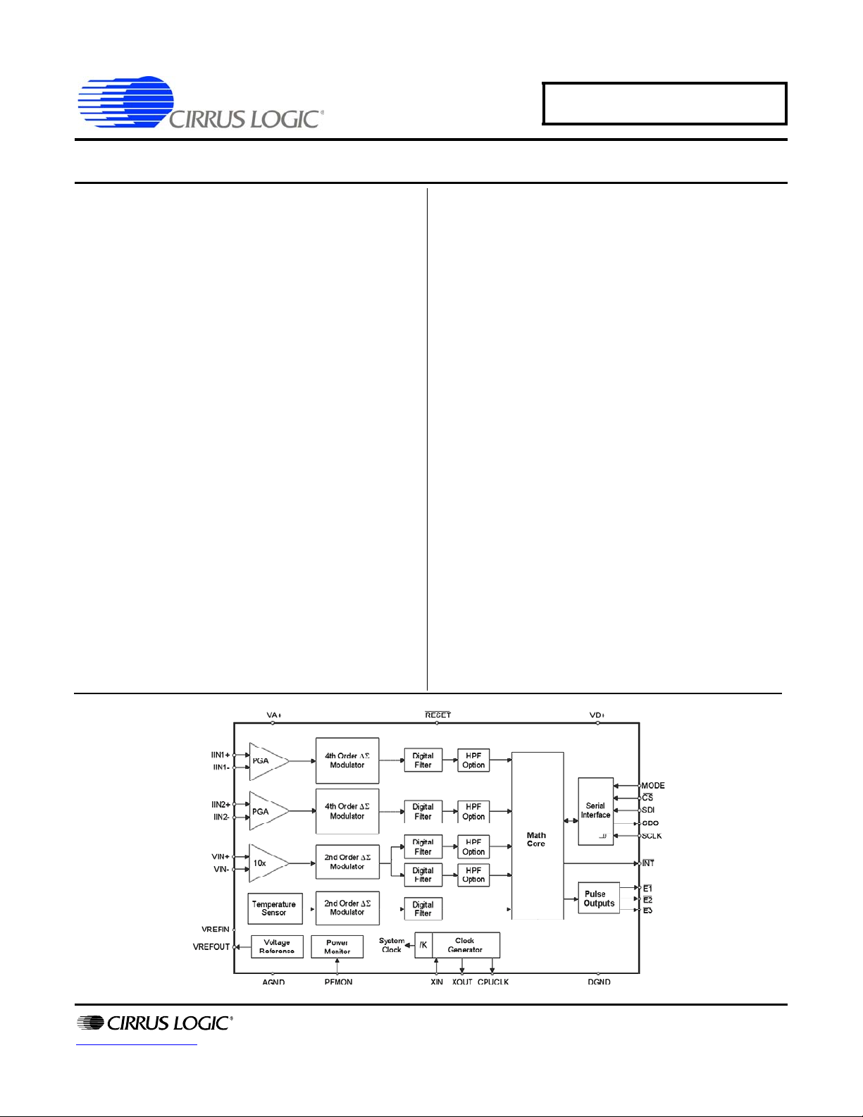
1. OVERVIEW
The CS5464 is a CMOS power measurement integrated circuit utilizing four analog-to-digital convert-
ers to measure line voltage, temperature, and current from up to two sources. It calculates active, reactive,
and apparent power as well as RMS and peak vo ltage an d curren t. It handles other system-related functions, such as pulse output conversion, voltage sag, current fault, voltage zero crossing, line frequency,
and tamper detection.
The CS5464 is optimized to interface to current transformers or shunt resistors for current measurement,
and to a resistive divider or voltage transformer for voltage measurement. Two full-scale ranges are provided on the current inputs to accommodate both types of current sensors. The second current channel
can be used for tamper detection or as a second current input. The CS5464’s three differential inputs have
a common-mode input range from analog ground (AGND) to the positive analog supply (VA+).
An additional analog input (PFMON) is provided to allow the application to determine when a power failure
is in progress. By monitoring the unregulated power supply, the application can take any required action
when a power loss occurs.
An on-chip voltage reference (nominally 2.5 volts) is generated and provided at analog output, VREFOUT.
This reference can be supplied to the chip by connecting it to the reference voltage input, VREFIN. Alternatively, an external voltage reference can be supplied to the reference input.
Three digital outputs (E1
ed, provide energy pulses, power failure indication, or other choices.
The CS5464 includes a three-wire serial host interface to an external microcontroller or serial E
Signals include serial data input (SDI), serial data output (SDO), serial clock (SCLK), and optionally, a
chip select (CS
used to control whether an E
), which allows the CS5464 to share the SDO signal with other devices. A MODE input is
, E2, E3) provide a variety of output signals and, depending on the mode select-
2
PROM.
2
PROM will be used instead of a host microcontroller.
DS682F3 5
Page 6
CS5464
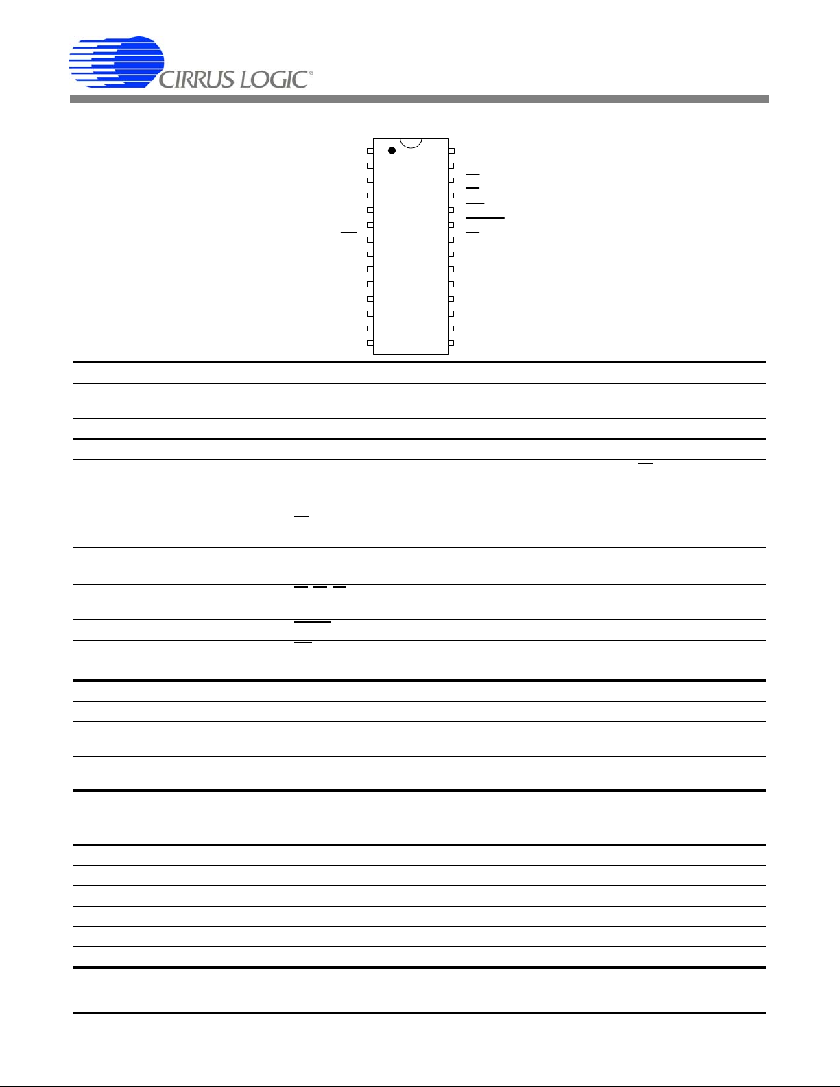
VREFIN 12Voltage Reference Input
VREFOUT 11Voltage Reference Output
VIN- 10Differential Voltage Input
VIN+ 9Differential Voltage Input
MODE 8Mode Select
CS 7Chip Select
SDO 6Serial Data Ouput
SCLK 5Serial Clock
DGND 4Digital Ground
VD+ 3Positive Digital Supply
CPUCLK 2CPU Clock Output
XOUT 1Crystal Out
AGND17 Analog Ground
VA+
18 Positive Analog Supply
IIN1-19 Differential Current Input
IIN1+20 Differential Current Input
PFMON21 P o w e r F a il M o nitor
E322 Energy Output 3
RESET23 Reset
INT24 Interrupt
E125 Energy Output 1
26
SDI27 Serial Data Input
XIN28 Crystal In
E2
Energy Output 2
TEST2 14Factory Test
TEST1 13Factory Test
IIN2 -15 Differential Current Input
IIN2 +16 Differential Current Input
2. PIN DESCRIPTION
Clock Generator
Crystal Out
Crystal In
CPU Clock Output 2
Control Pins and Serial Data I/O
Serial Clock 5
Serial Data Output 6
Chip Select 7
Mode Select 8
Energy Outputs 22, 25,
Reset 23
Interrupt 24
Serial Data Input 27
Analog Inputs/Outputs
Differential V ol tage Inputs 9,10
Differential Current Inputs 20,19,
Power Fail Monitor 21
Voltage Reference Output 11
Voltage Reference Input 12
Power Connections
Positive Digital Supply 3
Digital Ground 4
Positive Analog Supply 18
Analog Ground 17
Other Pins
Test1, Test2 13,14
6 DS682F3
1,28
XOUT, XIN — Connect to an external quartz crystal. Alternatively, an external clock can be supplied to the XIN pin to provide the system clock for the device.
CPUCLK - Logic-level output from crystal oscillator. Can be used to clock an external CPU.
SCLK — Clocks serial data from the SDI pin and to the SDO pin when CS is low. SCLK is a
Schmitt-trigger input when MODE is low and a driven output when MODE is high.
SDO — Serial data output. Data is clocked out by SCLK.
CS — An input that enables the serial interface when MODE is low and a driven output when
MODE is high.
MODE — High selects external E2PROM, Low selects external microcontroller. MODE includes a
weak internal pull-down and therefore selects microcontroller mode if not connected.
E3, E1, E2 — Primarily active-low energy pulse outputs. These can be programmed to output
other conditions.
26
RESET — An active-low Schmitt-trigger input used to reset the chip.
INT — Active-low output, indicates that an enabled condition has occurred.
SDI — Serial data input. Data is clocked in by SCLK.
VIN+, VIN- — Differential analog inputs for the voltage channel.
IIN1+, IIN1-, IIN2+, IIN2- — Differential analog inputs for the current channels.
16,15
PFMON — Used to monitor the unregulated power supply via a resistive divider. If the PFMON
voltage drops below its low limit, the low-supply detect (LSD) bit is set in the Status register.
VREFOUT — The on-chip voltage reference output. Nominally 2.5 V, referenced to AGND.
VREFIN — The voltage reference input. Can be connected to VREFOUT or external 2.5 V refer-
ence.
VD+ — The positive digital supply.
DGND — Digital ground.
VA+ — The positive analog supply.
AGND — Analog ground.
NC — Factory use only. Connect to AGND.
Page 7
CS5464
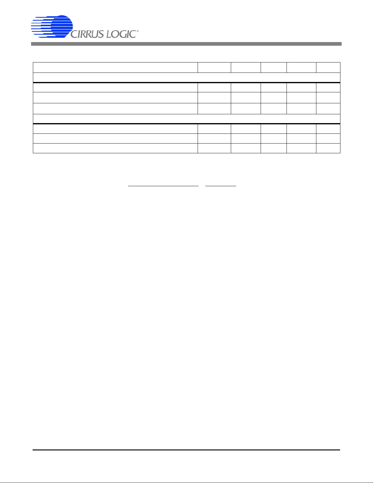
3. CHARACTERISTICS & SPECIFICATIONS
RECOMMENDED OPERATING CONDITIONS
Parameter Symbol Min Typ Max Unit
Positive Digital Power Supply VD+ 3.135 5.0 5.25 V
Positive Analog Power Supply VA+ 4.75 5.0 5.25 V
Voltage Reference VREFIN - 2.5 - V
Specified Temperature Range T
A
ANALOG CHARACTERISTICS
• Min / Max characteristics and specifications are guaranteed over all Recommended Operating Conditions .
• Typical characteristics and specifications are measured at nominal supply voltages and TA = 25 °C.
• VA+ = VD+ = 5 V ±5%; AGND = DGND = 0 V; VREFIN = +2.5 V. All voltages with respect to 0 V.
• DCLK = 4.096 MHz.
Parameter Symbol Min Typ Max Unit
Accuracy
Active Power
(Note 1) Input Range 0.1% - 100%
Reactive Power
(Note 1 and 2) Input Range 0.1% - 100%
Power Factor
(Note 1 and 2) Input Range 1.0% - 100%
Input Range 0.1% - 1.0%
Current RMS
(Note 1) Input Range 1.0% - 100%
Input Range 0.1% - 1.0%
Volt age RMS
(Note 1) Input Range 5% - 100%
Analog Inputs (All Inputs)
Common Mode Rejection
Common Mode + Signal -0.25 - VA+ V
Analog Inputs (Current Inputs)
Differential Input Range
[(IIN+) – (IIN-)] (Gain = 50)
Total Harmonic Distortion (Gain = 50) THD 80 94 - dB
Crosstalk from Voltage Input at Full Scale
Input Capacitance IC - 27 - pF
Effective Input Impedance EII 30 - - k
Noise (Referred to Input)
Offset Drift (Without the High-pass Filter) OD - 4.0 - µV/°C
Gain Error
Notes: 1. Applies when the HPF option is enabled.
2. Applies when the line frequency is equal to the product of the output word rate (OWR) and the value of
Epsilon.
All Gain Ranges
All Gain Ranges
All Gain Ranges
P
Active
Q
Avg
PF -
All Gain Ranges
I
RMS
All Gain Ranges
(DC, 50, 60 Hz) CMRR 80 - - dB
(Gain = 10)
(50, 60 Hz) --115-dB
(Gain = 10)
(Gain = 50)
(Note 3) GE - ±0.4 %
V
RMS
IIN
N
I
-40 - +85 °C
-±0.1-%
-±0.2-%
±0.2
-
±0.27
-
-
%
%
%
-
-
±0.1
±0.17
-
-
%
%
-±0.1-%
-
-
-
-
500
100
-
-
-
-
22.5
4.5
mV
mV
µV
µV
P-P
P-P
rms
rms
DS682F3 7
Page 8
CS5464
PSRR 20
150
V
eq
--------- -
log=
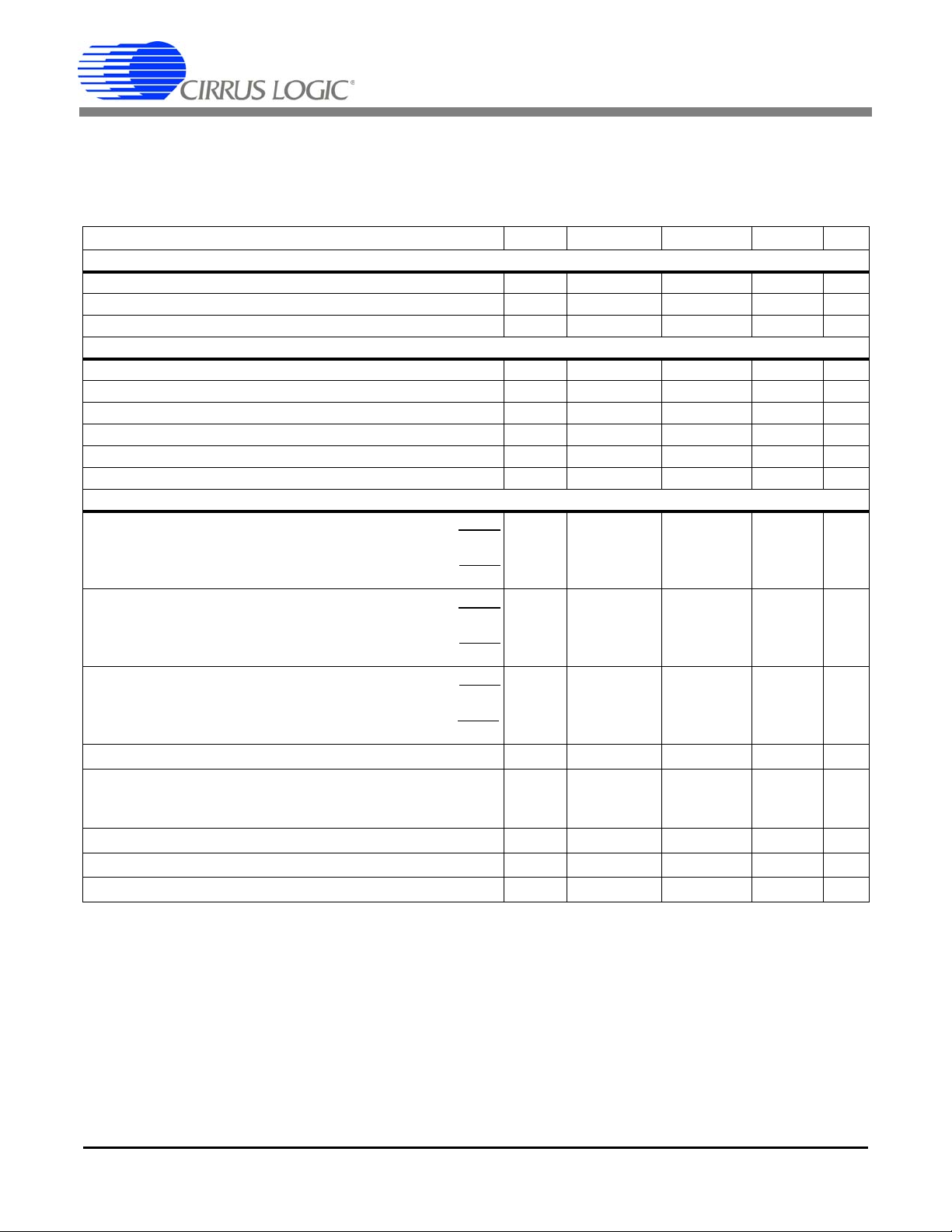
ANALOG CHARACTERISTICS (Continued)
Parameter Symbol Min Typ Max Unit
Analog Inputs (Voltage Inputs)
Differential Input Range
Total Harmonic Distortion THD 65 75 - dB
Crosstalk from Current Inputs at Full Scale
Input Capacitance
Effective Input Impedance EII 2 - - M
Noise (Referred to Input) N
Offset Drift (Without the High-pass Filter) OD - 16.0 - µV/°C
Gain Error
Temperature
Temperature Accuracy T - ±5 - °C
Power Supplies
Power Supply Currents (Active State)
(VA+ = 5V, VD+ = 3.3 V)
I
D+
Power Consumption
(Note 4) Active State (VA+ = 5 V, VD+ = 3.3 V)
Power Supply Rejection Ratio
(Note 5)
Active State (VA+ = VD+ = 5 V)
(50, 60 Hz)
PFMON Low-voltage Trigger Threshold
PFMON High-voltage Power-on Trip Point
[(VIN+) – (VIN-)] VIN - 500 - mV
(50, 60 Hz) --70-dB
All Gain Ranges IC - 2.0 - pF
--140µV
-
-
-
-
-
-
-
48
68
60
1.5
3.5
2.3
25
15
7
10
55
75
65
33
20
(Note 3) GE - ±3.0 %
I
I
(VA+ = VD+ = 5V)
D+
Stand-by State
Sleep State
Voltage
Current
(Gain = 50x)
Current (Gain = 10x)
(Note 6) PMLO 2.3 2.45 - V
(Note 7) PMHI - 2.55 2.7 V
V
PSCA
A+
PSCD
PSCD
PC
PSRR
P-P
rms
-
-
-
mA
mA
mA
mW
mW
-
-
-
-
-
mW
uW
dB
dB
dB
Notes: 3. Applies before system calibration.
4. All outputs unloaded. All inputs CMOS level.
5. Measurement method for PSRR: VREFIN tied to VREFOUT, VA+ = VD+ = 5 V, a 150 mV
(zero-to-peak) (60 Hz) sinewave is imposed onto the +5 V DC supply voltage at VA+ and VD+ pins. The
“+” and “-” input pins of both input ch annels a re sh or ted to AGND. T he CS5 464 is then command ed to
continuous conversion acquisition mode, and digital output data is collected for the chan nel under test.
The (zero-to-peak) value of the digital sinusoidal out put signal is determined, and this value is converted
into the (zero-to-peak) value of the sinusoidal voltage (me asured in m V) that would need to be applied
at the channel’s inputs, in order to cause the sa me digital sinusoidal output. This voltage is then defined
as Veq. PSRR is (in dB)
:
6. When voltage level on PFMON is sagging, and LSD bit = 0, the voltage at which LSD is set to 1.
7. If the LSD bit has been set to 1 (because PFMON voltage fell below PMLO), this is the voltage level on
PFMON at which the LSD bit can be permanently reset back to 0.
8 DS682F3
Page 9
CS5464
(VREFOUTMAX - VREFOUTMIN)
VREFOUT
AVG
(
(
1
T
A
MAX
- T
A
MIN
(
(
1.0 x 10
(
(
6
TC
VREF
=
VOLTAGE REFERENCE
Parameter Symbol Min Typ Max Unit
Reference Output
Output Voltage VREFOUT +2.4 +2.5 +2.6 V
Temperature Coefficient
Load Regulation
Reference Input
Input Voltage Range VREFIN +2.4 +2.5 +2.6 V
Input Capacitance - 4 - pF
Input CVF Current - 100 - nA
Notes: 8. The voltage at VREFOUT is measured across the temperature range. From these measurements the
following formula is used to calculate the VREFOUT temperature coefficient:.
9. Specified at maximum recommended output of 1 µA, source or sink.
(Note 8) TC
(Note 9) V
VREF
R
- 40 - ppm/°C
-610mV
DS682F3 9
Page 10
CS5464
DIGITAL CHARACTERISTICS
• Min / Max characteristics and specifications are guaranteed over all Recommended Operating Conditions .
• Typical characteristics and specifications are measured at nominal supply voltages and TA = 25 °C.
• VA+ = VD+ = 5V ±5%; AGND = DGND = 0 V. All voltages with respec t to 0 V.
• DCLK = 4.096 MHz.
Parameter Symbol Min Typ Max Unit
Master Clock Characteristics
Master Clock Frequency
Master Clock Duty Cycle 40 - 60 %
CPUCLK Duty Cycle
Filter Characteristics
Phase Compensation Range
Input Sampling Rate
Digital Filter Output Word Rate
High-pass Filter Corner Frequency
Full-scale DC Calibration Range (Referred to Input)
Channel-to-channel Time-shift Error
Input/Output Characteristics
High-level Input Voltage
All Pins Except XIN and SCLK and RESET
Low-level Input Voltage (VD = 5 V)
All Pins Except XIN and SCLK and RESET
Low-level Input Voltage (VD = 3.3 V)
All Pins Except XIN and SCLK and RESET
High-level Output Voltage
Low-level Output Voltage
Input Leakage Current
3-state Leakage Current I
Digital Output Pin Capacitance C
Internal Gate Oscillator (Note 11) DCLK 2.5 4.096 20 MHz
(Note 12 and 13) 40 - 60 %
(60 Hz, OWR = 4000 Hz) -5.4 - +5.4 °
DCLK = MCLK/K - DCLK/8 - Hz
(Both channels) OWR - DCLK/1024 - Hz
-3 dB -0.5-Hz
(Note 14) FSCR 25 - 100 %FS
(Note 15) 1.0 µs
SCLK and RESET
SCLK and RESET
SCLK and RESET
I
out
I
=-5mA(VD=+5V)
out
= -2.5 mA (VD = +3.3V)
I
out
XIN
XIN
XIN
= +5 mA V
(Note 16) I
V
IH
0.6 VD+
(VD+) – 0.5
0.8VD+
V
IL
-
-
-
V
IL
-
-
-
(VD+) - 1.0 - - V
OH
V
OL
-
-
in
OZ
out
-±1±10µA
--±10µA
-5-pF
-
-
-
-
-
-
-
-
-
-
-
-
-
-
0.8
1.5
0.2VD+
0.48
0.3
0.2VD+
0.4
0.4
V
V
V
V
V
V
V
V
V
V
V
Notes: 10. All measurements performed under static conditions.
11. If a crystal is used, XIN frequency must remain between 2.5 MHz - 5.0 MHz. If an external oscillator is
used, XIN frequency range is 2.5 MHz - 20 MHz, but K must be set so that MCLK is between
2.5 MHz - 5.0 MHz.
12. If external MCLK is used, the duty cycle must be between 45% and 55% to maintain this specification.
13. The frequency of CPUCLK is equal to MCLK.
14. The minimum FSCR is limited by the maximum allowed gain register value. The maximum FSCR is
limited by the full-scale signal applied to the input.
15. Configuration register (Config) bits PC[6:0] are set to “0000000”.
16. The MODE pin is pulled low by an internal resistor.
10 DS682F3
Page 11
CS5464
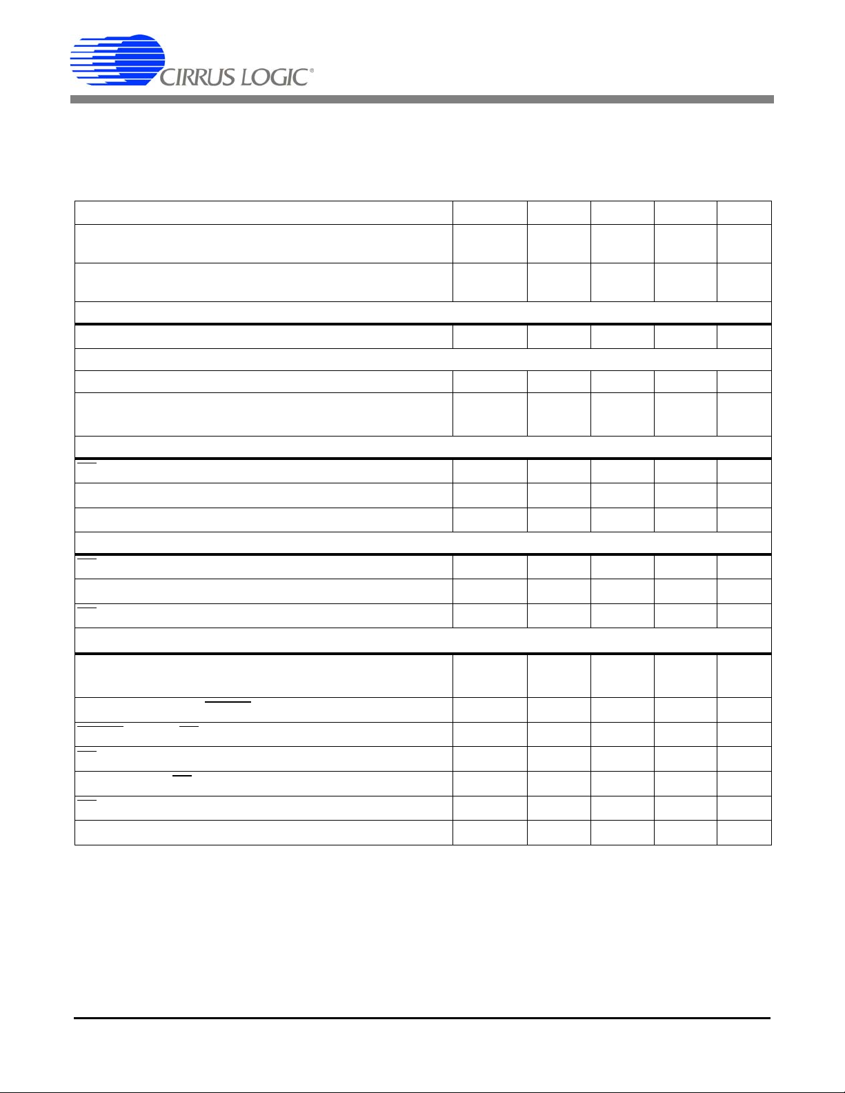
SWITCHING CHARACTERISTICS
• Min / Max characteristics and specifications are guaranteed over all Recommended Operating Conditions.
• Typical characteristics and specifications are measured at nominal supply voltages and TA = 25 °C.
• VA+ = 5 V ±5% VD+ = 3.3 V ±5% or 5 V ±5%; AGND = DGND = 0 V. All voltages with respect to 0 V.
• Logic Levels: Logic 0 = 0 V, Logic 1 = VD+.
Parameter Symbol Min Typ Max Unit
Rise Times
(Note 17)
Any Digital Output
Fall Times
(Note 17)
Any Digital Output
Start-up
Oscillator Start-up Time
XTAL = 4.096MHz (Note 11) t
Serial Port Timing
Serial Clock Frequency SCLK - - 2 MHz
Serial Clock
Pulse Width High
Pulse Width Low
SDI Timing
CS
Falling to SCLK Rising t
Data Set-up Time Prior to SCLK Rising t
Data Hold Time After SCLK Rising t
SDO Timing
Falling to SDO Driving t
CS
SCLK Falling to New Data Bit (hold time) t
Rising to SDO Hi-Z t
CS
2
E
PROM mode Timing
Serial Clock
MODE setup time to RESET
RESET
CS
SCLK falling to CS
CS
rising to CS falling t
falling to SCLK rising t
rising t
rising to driving MODE low t
Rising t
Pulse Width Low
Pulse Width High
SDO setup time to SCLK rising t
Notes: 17. Specified using 10% and 90% points on waveform of interest. Output loaded with 50 pF.
18. Oscillator start-up time varies with crystal parameters. This specification does not apply when using an
external clock source.
t
rise
t
t
fall
ost
t
1
t
2
3
4
5
6
7
8
t
9
10
11
12
13
14
15
16
-
-
-
-
50
50
-
-
1.0
-
1.0
-
µs
ns
µs
ns
-60-ms
200
200
-
-
-
-
ns
ns
50 - - ns
50 - - ns
100 - - ns
-2050ns
-2050ns
-2050ns
8
8
DCLK
DCLK
50 ns
48 DCLK
100 8 DCLK
16 DCLK
50 ns
100 ns
DS682F3 11
Page 12
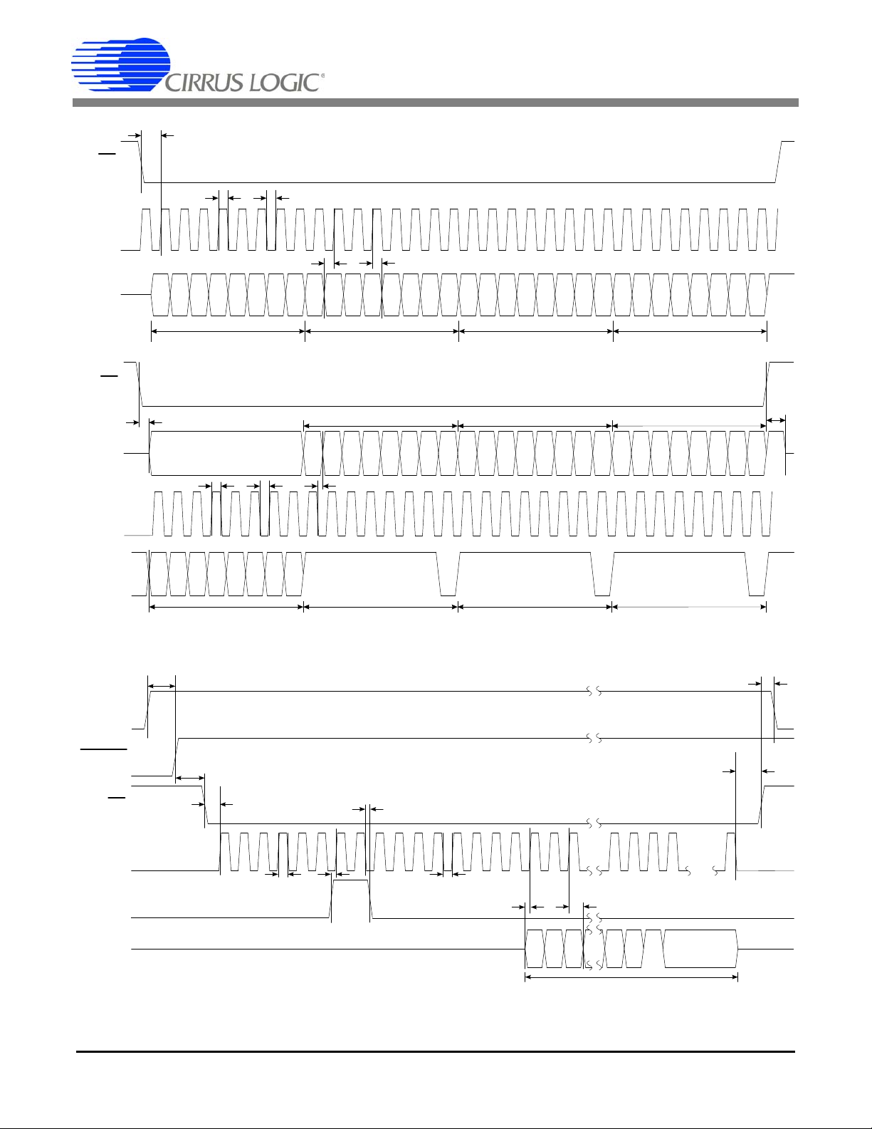
t
1
t
2
t
3
t
4
t
5
MSB
MSB-1
LSB
MSB
MSB-1
LSB
MSB
MSB-1
LSB
MSB
MSB-1
LSB
Com m and Tim e 8 SC LKs H igh Byte Mid Byte Low Byte
CS
SCLK
SDI
t
10
t
9
RESET
SDO
SCLK
CS
Last 8
Bits
SDI
MODE
STOP bit
D a ta fro m EE P R O M
t
16
t
4
t
5
t
14
t
15
t
7
t
13
t
12
t
11
(INPUT)
(INPUT)
(O UT P U T )
(O UT P U T )
(O UT P U T )
(INPUT)
t
1
t
2
MSB
MSB-1
LSB
Comm and Time 8 SC LKs
SYNC0 or SYNC1
Command
SYNC0 or SYNC1
Comm and
MSB
MSB-1
LSB
MSB
MSB-1
LSB
MSB
MSB-1
LSB
Hig h Byte M id B yte Low B yte
CS
SDO
SCLK
SDI
t
6
t
7
t
8
SYNC0 or SYNC1
Comm and
UNKNOWN
SDI Write Timing (Not to Scale)
SDO Read Timing (Not to Scale)
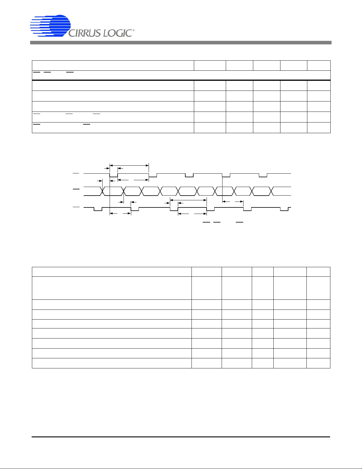
Figure 1. CS5464 Read and Write Timing Diagrams
E2PROM mode Sequence Timing (Not to Scale)
CS5464
12 DS682F3
Page 13
CS5464
t
period
E1
t
3
t
4
t
5
t
3
t
5
t
4
E2
E3
t
pw
t
period
t
pw
Figure 2. Timing Diagram for E1, E2, and E3
SWITCHING CHARACTERISTICS (Continued)
Parameter Symbol Min Typ Max Unit
E1
, E2, and E3 Timing (Note 19 and 20)
Period t
Pulse Width t
Rising Edge to Falling Edge t
Setup to E1 and/or E3 Falling Edge t
E2
Falling Edge to E3 Falling Edge t
E1
period
pw
3
4
5
Notes: 19. Pulse output timing is specified at DCLK = 4.096 MHz, E2MODE = 0, and E3MODE[1:0] = 0. Refer to
6.7 Energy Pulse Outputs on page 19 for more information on pulse output pins.
20. Timing is proportional to the frequency of DCLK.
500 - - s
244 - - s
6--s
1.5 - - s
248 - - s
ABSOLUTE MAXIMUM RATINGS
WARNING: Operation at or beyond these limits may result in permanent damage to the device.
Normal operation is not guaranteed at these extremes
Parameter Symbol Min Typ Max Unit
DC Power Supplies
Input Current, Any Pin Except Supplies
(Notes 21 and 22)
Positive Digital
Positive Analog
(Notes 23, 24, 25) I
Output Current, Any Pin Except VREFOUT I
Power Dissipation
Analog Input Voltage
Digital Input Voltage
(Note 26) PD --500mW
All Analog Pins V
All Digital Pins V
Ambient Operating Temperature T
Storage Temperature T
Notes: 21. VA+ and AGND must satisfy [(VA+) - (AGND)] + 6.0 V.
22. VD+ and AGND must satisfy [(VD+) - (AGND)] + 6.0 V.
23. Applies to all pins including continuous over-voltage conditions at the analog input pins.
24. Transient current of up to 100 mA will not cause SCR latch-up.
25. Maximum DC input current for a power supply pin is ±50 mA.
26. Total power dissipation, including all input currents and output currents.
.
VD+
VA+
IN
OUT
INA
IND
A
stg
-0.3
-0.3
--±10mA
--100mA
- 0.3 - (VA+) + 0.3 V
-0.3 - (VD+) + 0.3 V
-40 - 85 °C
-65 - 150 °C
-
-
+6.0
+6.0
V
V
DS682F3 13
Page 14
4. SIGNAL PATH DESCRIPTION
Figure 3. Signal Flow for V1, I1, P1, Q1 Measurements
FGA
V1
OFF
V1
GAIN
I1
OFF
I1
GAIN
Figure 4. Signal Flow for V2, I2, P2, Q2 Measurements
V2
OFF
V2
GAIN
I2
OFF
I2
GAIN
The data flow for voltage and current measurement and
the other calculations are shown in Figures 3, 4, and 5.
The data flow consists of two current
paths. Both voltage paths are derived from the
age
same differential input pins. Each curr ent path has its
own differential input pins.
4.1 Analog-to-Digital Converters
The voltage and temperature channels use second-order delta-sigma modulators and the two current channels use fourth-order delta-sigma modulators to convert
the analog inputs to single-bit digital data streams. The
converters sample at a rate of DCLK/8. This high sampling provides a wide dynamic range and simplifies anti-alias filter design.
4.2 Decimation Filters
The single-bit modulator output data is widened to
24 bits and down-sampled to DCLK/1024 with low-pass
paths and two vo lt-
CS5464
decimation filters. These decimation filters ar e third-order Sinc. Their outputs are passed through third-order
IIR “anti-sinc” filters, used to compensate for the amplitude roll-off of the decimation filters.
4.3 Phase Compensation
Phase compensation changes the ph ase of curren t relative to voltage by changing the sampling time in the
decimation filters. The amount of phase shift is set by
bits PC[7:0] in the Configuration register
channel 1 and bits PC[7:0] in the Control register (
for channel 2.
Phase compensation, PC[7:0] is a signed two’s complement binary value in the rang e of -1.0 to almost +1.0
output word rate (OWR) samples. Fo r a sample rate of
4000 Hz, the delay range is ±250
S, a phase shift of
±4.5° at 50 Hz and ±5.4° at 60 Hz. The step size would
be 0.0352° at 50 Hz and 0.0422° at 60 Hz at this sample
rate.
(Config) for
Ctrl)
14 DS682F3
Page 15

CS5464
I
RMS
I
n
n0=
N1–
N
-------------------- -
=
2
4.4 DC Offset and Gain Correction
The system and chip inherently have gain and offset errors which can be removed using t he gain and offset
registers. (See Section 9.
39). Each measurement channel has its own registers.
For every channel, the output of the IIR filter is added to
the offset register and multiplied by the gain register.
System Calibration on page
4.5 High-pass Filters
Optional high-pass filters (HPF in Figures 3 and 4) remove any DC from the selected signal paths. Subsequently, DC will also be removed from power, and all
low-rate results. (see Figures 5).
Each energy channel has a current and voltage path. If
an HPF is enabled in only one path, a phase-matching
filter (PMF) is applied to the other path which matches
the amplitude and phase delay of the HPF in the band
of interest, but passes DC. For more information, see
High-pass Filters on page 19. The HPF filter multi-
6.5
plexers drive the
I1, V1, I2, and V2 result registers.
4.6 Low-Rate Calculations
Low-rate results are derived from sample-rate results
integrated over
in the Cycle Count register. The low-rate interval is the
sample interval multiplied by
N samples, where N is the value stored
N.
4.7 RMS Results
The root mean square (RMS in Figure 5) calculations
are performed on
samples, using the formula:
N instantaneous voltage and current
DS682F3 15
Page 16

CS5464
V1
ACOFF
(V2
ACOFF
)
I1
ACOFF
(I2
ACOFF
)
P1
OFF
(P2
OFF
)
Figure 5. Low-rate Calculations
SV
RMSIRMS
=
PF
P
ACTIVE
S
----------------------
=
Q
WB
S2P
ACTIVE
2
–=
4.8 Power and Energy Results
The instantaneous voltage and current samples are
multiplied to obtain the instantaneous power (
(see Figure 3 and 4). The product is then average d over
N conversions to compute active power (P1
P2
).
AVG
Apparent power (
S1, S2) is the product of RMS voltage
and current as shown:
Power factor (
PF1, PF2) is active power divided by ap-
parent power as shown below. The sign of the power
factor is determined by the active power.
Q1
Wideband reactive power (
, Q2WB) is calculated
WB
by doing a vector subtraction of active power from apparent power.
Quadrature power (
Q1, Q2) are sample rate results ob-
tained by multiplying instantaneous current (
stantaneous quadrature voltage (
V1Q, V2Q) which are
created by phase shifting instantaneous voltage (
V2) 90 degrees using first-order integr ators. (see Figure
3 and 4). The gain of these integrators is inversely relat-
P1, P2)
AVG
I1, I2) by in-
V1,
ed to line frequency, so their gain is corrected by the
silon
register, which is based on line frequency.
Reactive power (
grating the instantaneous quadrature power over
,
samples.
Q1
AVG
, Q2
) is generated by inte-
AVG
4.9 Peak Voltage and Current
Peak current (I1
(
V1
PEAK
,
V2
PEAK
samples detected in the previous low-rate interval.
PEAK
, I2
) and peak voltage
PEAK
) are the largest current and voltage
4.10 Power Offset
The power offset registers, P1
to offset erroneous power sources resident in the system not originating from the power line. Residual power
offsets are usually caused by crosstalk into current
paths from voltage paths or from ripple on the meter or
chip’s power supply, or from inductance from a nearby
transformer.
These offsets can be either positive or negative, indicating crosstalk coupling either in phase or out of phase
with the applied voltage input. The power offset registers can compensate for either condition.
To use this feature, measure the average power at no
load using either Single or Continuous Conversion commands. Take the measured result (from the
(P2
) register), invert (negate) the value and write it
AVG
to the associated power offset register,
OFF
(P2
) can be used
OFF
P1
OFF
(P2
P1
Ep-
AVG
OFF
N
).
16 DS682F3
Page 17

5. PIN DESCRIPTIONS
Figure 6. Oscillator Connections
Oscillator
Circuit
DGND
XIN
XOUT
C1
C1 =
22 pF
C2
C2 =
CS5464
5.1 Analog Pins
The CS5464 has three differential inputs: VINIIN1,
and IIN2
respectively. A single-ended power fail monitor input,
voltage reference input, and voltage reference output
are also available.
are the voltage, current1, and current2 inputs,
5.1.1 Voltage Inputs
The output of the line voltage resistive divider or transformer is connected to the VIN+ and VIN- input pins of
the CS5464. The voltage channel is equipped with a
10x, fixed-gain amplifier. The full-scale signal level that
can be applied to the voltage channel is ±250mV. If the
input signal is a sine wave, the maximum RMS voltage
is 250mVp /
mately 70.7% of maximum peak voltage.
2 176.78mVRMS which is approxi-
5.1.2 Current1 and Current2 Inputs
The output of the current-sensing resistor or transformer is connected to the IIN1+ (IIN2+) and IIN1- (IIN2-) input pins of the CS5464. To accommodate different
current-sensing elements, the cu rrent chan nel incorporates a programmable gain amplifier (PGA) with two selectable input gains. The full-scale signal level for the
current channels is ±50mV or ±250mV. If the input signal is a sine wave, the maximum RMS voltage is
35.35mVRMS or 176.78mVRMS which is approximately 70.7% of maximum peak voltage.
5.1.3 Power Fail Monitor Input
An analog input (PFMON) is provided to determine
when a power loss is imminent. By connecting a resistive divider from the unregulated meter power supply to
the PFMON input, an interrupt can be generated, or the
Low Supply Detected (LSD)
monitored to indicate low-supply conditions. The PFMON input has a comparator that trips around the level
of the voltage reference input (VREFIN).
Status register bit can be
5.1.4 Voltage Reference Input
The CS5464 requires a stable voltage reference of
2.5 V applied to the VREFIN pin. This reference can be
supplied from an external voltage reference or from the
VREFOUT output. A bypass capacitor of at least 0.1
is recommended at the VREFIN pin.
5.1.5 Voltage Reference Output
The CS5464 generates a 2.5 V reference (VREFOUT).
It is suitable for driving the VREFIN pin, but has very little fan-out and is not recommended for driving external
circuits.
5.1.6 Crystal Oscillator
An external quartz crystal can be connected to the XIN
and XOUT pins as shown in Figure 6. To reduce system
cost, each pin is supplied with an on-chip, phase-shifting capacitor to ground.
.
Alternatively, an external clock source can be connected to the XIN pin.
5.2 Digital Pins
5.2.1 Reset Input
The active-low RESET pin, when asserted, will halt all
CS5464 operations and reset internal hardware registers and states. When de-asserted, an initialization sequence begins, setting default register values.
5.2.2 CPU Clock Output
A logic-level clock output (CPUCLK) is provided at the
crystal frequency to drive an external CPU or microcontroller clock. Two phase choices are available.
5.2.3 Interrupt Output
The INT pin indicates an enabled Internal Stat us regis-
Status) bit is set. Status register bits indicate condi-
ter (
tions such as data ready, modulator oscillations, low
supply, voltage sag, current faults, numerical overflows,
and result updates.
F
5.2.4 Energy Pulse Outputs
The CS5464 provides three pins (E1, E2, E3) for pulse
energy outputs. These pins can also be used to output
other conditions, such as voltage sign, power fail monitor, or energy channel in use.
DS682F3 17
Page 18

CS5464
5.2.5 Serial Interface
The CS5464 provides 5 pins, SCLK, SDI, SDO, CS, and
MODE for communication between a host microcontroller or serial E
MODE is an input that, when high, indicates to the
CS5464 that a serial E
a host microcontroller. It has a weak pull-down allowing
it to be left unconnected if microcontroller mode is used.
SCLK is used to shift and qualify serial data. Serial data
changes as a result of the falling edge of SCLK and is
valid during the rising edge. It is a Schmitt-trigger input
2
PROM and the CS5464.
2
PROM is being used instead of
for host microcontrollers, and a driven output for serial
2
PROMs.
E
SDI is the serial data input to the CS5464.
SDO is the serial data output from the CS546 4. It’s out-
put drivers are disabled whenever CS
lowing other devices to drive the SDO line.
is the chip select input for the serial bus. A high logic
CS
level de-asserts it, tri-stating the SDO pin and clearing
the serial interface. A low logic level enables the serial
port. This pin may be tied low for systems not requiring
multiple SDO drivers. CS
facing to serial E
2
PROMs.
is a driven output when inter-
is de-asserted, al-
18 DS682F3
Page 19

6. SETTING UP THE CS5464
CS5464
6.1 Clock Divider
The internal clock to the CS5464 needs to operate
around 4 MHz. However, by using the internal clock divider, a higher crystal frequency can be used. This is important when driving an external microcontroller
requiring a faster clock and using the CPUCLK output.
K is the divide ratio from the crystal input to the internal
clock and is selected with Configuration
fig
) bits K[3:0]. It has a range of 1 to 16. A value of zero
results in a setting of 16.
register (Con-
6.2 CPU Clock Inversion
By default, CPUCLK is inverted from XIN. Setting Configuration
can be useful when one phase adds more noise to the
system than the other.
register bit iCPU removes this inversion. This
6.3 Interrupt Pin Behavior
The behavior of the INT pin is controlled by the IMODE
and IINV bits in the Configuration
IMODE IINV INT Pin
0 0 Active-low Level
0 1 Active-high Level
10 Low Pulse
11 High Pulse
Table 1. Interrupt Configuration
If IMODE = 1, the duration of the INT
DCLK cycles, where DCLK = MCLK/K.
register as shown.
pulse will be two
6.4 Current Input Gain Ranges
Control register bits I1gain (I2gain) select the input
range of the current inputs.
I1gain, I2gain Maximum Input
0±250mV10x
1 ±50 mV 50x
Table 2. Current Input Gain Ranges
Gain
6.5 High-pass Filters
Mode Control (Modes) register bi ts VHPF and IHPF activate the HPF in the voltage and current paths, respectively. Each energy channel has separate VHPF and
IHPF bits. When a high-pass filter is enabled in only one
path within a channel, a phase matching filter (PMF) is
applied to the other path within that channel. The PMF
filter matches the amplitude and phase response of the
HPF in the band of interest, but passes DC.
VHPF IHPF Filter Configuration
0 0 No filter on Voltage or Current
0 1 HPF on Current, PMF on Voltage
1 0 HPF on Voltage, PMF on Current
1 1 HPF on Current and V oltage
Table 3. High-pass Filter Configuration
6.6 Cycle Count
Low-rate calculations, such as average power and RMS
voltage and current integrate over several (
word rate (OWR) samples. The duration of this averaging window is set by the Cycle Count (
fault, Cycle Count is set to 4000 (1 second at output
word rate [OWR] of 4000 Hz). The minimum value for
Cycle Count is 10.
N) register. By de-
N) output
6.7 Energy Pulse Outputs
By default, E1 outputs active energy, E3, reactive energy, and E2
(See Figure 2.
page 13.)
Three pairs of bits in the Mode Control (
control the operation of these outputs. These bits are
named E1MODE[1:0], E2MODE[1:0], and
E3MODE[1:0]. Some combinations of these bits override others, so read the following paragraphs carefully.
The E2
energy channel in use (1 or 2). Table 4 lists the functions of E2
register.
Note: E2MODE[1:0]=3 is a special mode.
E2MODE1 E2MODE0 E2
The E3
itor status, voltage sign, or apparent energy. Table 5
, the sign of both active and reactive energy.
Timing Diagram for E1, E2, and E3 on
Modes) register
pin can output energy sign, apparent energy, or
as controlled by E2MODE[1:0] in the Modes
output
0 0 Energy Sign
0 1 Apparent Energy
1 0 Channel in Use
1 1 Enable E1MODE
Table 4. E2 Pin Configuration
pin can output reactive energy, power fail mon-
DS682F3 19
Page 20

CS5464
lists the functions of E3 as controlled by E3MODE[1:0]
Modes register when E1MODE is not enabled.
in the
E3MODE1 E3MODE0 E3 output
0 0 Reactive Energy
0 1 Power Fail Monitor
1 0 Voltage Sign
1 1 App arent Energy
Table 5. E3 Pin Configuration
When both E2MODE bits are high, the E1MODE bits
are enabled, allowing active, apparent, reactive, or
wideband reactive energy for
be output on E1
and E2. Table 6 lists the functions of E1
both energy channels to
and E2 with E1MODE enabled.
E1MODE1 E1MODE0 E1
/ E2 outputs
0 0 Active Energy
0 1 App arent Energy
1 0 Reactive Energy
1 1 Wideband Reactive
Ta bl e 6. E1 / E2 Modes
When E1MODE bits are enabled, the E3
pin outputs either the power fail monitor status, or the sign of the E1
and E2 outputs. Table 7 list the functions of the E3 pin
using E3MODE[1:0] in the
E1MODE is enabled
.
E3MODE1 E3MODE0 E3
Modes register when
output
0 0 Power Fail Monitor
0 1 Energy Sign
1 0 not used
1 1 not used
Ta bl e 7. E3 Pin with E1MODE enabled
6.8 No Load Threshold
The No Load Threshold register (Load
zero out the contents of
E
their magnitude is less than the
PULSE
and Q
Load
) is used to
MIN
registers if
PULSE
register value.
MIN
6.9 Energy Pulse Width
Note: Energy Pulse Width (PulseWidth) only applies to
, E2, or E3 pins that are configured to output pulses.
E1
When any are configured to output steady-state signals,
such as voltage sign, energy channel in use, power fail
monitor, or energy sign, pulse widths and output rates
do not apply.
The pulse width time (t
PulseWidth register which is an integer multiple of
in the
the sample or output word rate (OWR).
4000 Hz (a period of 250 uS) t
By default,
PulseWidth is set to 1.
) in Figure 2, is set by the value
pw
At OWR of
= PulseWidth x 250uS.
pw
6.10 Energy Pulse Rate
The full-scale pulse frequency of enabled E1, E2, E3
pins is the PulseRate x output word rate (OW R)/2. Th e
actual pulse frequency is the full-scale pulse frequency
multiplied by the pulse register’s (
Q
PULSE
) value.
E
PULSE
, S
PULSE
Example:
If the output word rate (OWR) is 4000 Hz, and the
PulseRate is set to 0.05, the full-rate pulse frequency is
0.05 x 4000 / 2 = 100 Hz. If the
, is 0.4567, the pulse output rate on E1 will be
E1
E
register, driving
PULSE
100 Hz x 0.4567 = 45.67 Hz.
6.11 Voltage Sag/Current Fault Detection
Voltage sag detection is used to determine when averaged voltage falls below a predetermined level for a
specified interval of time. Current fault detection determines when averaged current falls below a predetermined level for a specified interval of time.
The specified interval of time (duration) is set by the value in the
(I2Fault
V1Sag
) registers. Setting any of these to zero (de-
DUR
fault) disables the detect feature for the given channel.
The value is in output word rate (OWR) samples. The
predetermined level is set by the values in the
V1Sag
(I2Fault
LEVEL
LEVEL)
(V2Sag
registers.
Since the values of
put, only one voltage sag detector is necessary.
DUR
(V2Sag
) and I1Fault
LEVEL
) and I1Fault
DUR
DUR
LEVEL
V1 and V2 come from the same in-
,
20 DS682F3
Page 21

CS5464
Figure 7. Sag and Fault Detect
For each enabled input channel, the measured value is
rectified and compared to the associ at ed leve l re gis te r
Over the duration window, the number of samples
above and below the level are counted. If the number of
samples below the level exceeds the number of samples above, a
FAULT
(I2
FAULT
I1
Status register bit V1
) is set, indicating a sag or fault condi-
SAG
(V2
SAG
tion. (see Figure 7)..
6.12 Epsilon
The Epsilon reg ister is used to set the gain of the 90°
phase shift used in the quadrature power calculation.
The value in the
Epsilon register is the ratio of the line
frequency to the output word rate (OWR). It is, by default, 50/4000 (0.0125), for 50 Hz line and 4000 Hz
sample (OWR) frequencies.
For 60 Hz line frequency, it is 60/400 0 (0.015). Other
output word rates (OWR) can be used.
Epsilon can also be calculated automatically by the
CS5464 by setting the AFC bit in the Mode Control
Modes) register. The Frequency Update bit (FUP) in
(
Status register is set every time the Epsilon re gister
the
has been automatically updated.
6.13 Temperature Measurement
The on-chip temperature sensor is designed to measure temperature and optionally compensate for temperature drift of the voltage reference. It uses the V
a transistor to determine temperature.
Temperature measurements are stored in the Temperature register (
T) which, by default, is configured to a
range of ±128 degrees on the Celsius (°C) scale.
BE of
The application program can change both the scale and
.
range of Temperature (
T
Gain (
GAIN
) and Temperature Offset (T
T) by changing the T emperature
OFF
Two values must be known — the transistor’s
degree, and the transistor’s V
),
time of this publication, these values are:
BE at 0 degrees. At the
VBE (per degree) = 0.2769523 mV/°C or °K
V
0 = 79.2604368 mV at 0°C
BE
To determine the values to write to
the following formulae:
T
= ADFS / VBE / TFS x 2
GAIN
T
= -VBE0 / ADFS x 2
OFF
23
In the above equations, ADFS is the full-scale input
range of the temperature A/D conv er te r o r 83 3.333 mV
and T
is the desired full-scale range of the Tempera-
FS
ture register. The binary exponents are the bit positions
of the binary point of these registers.
To use the Celsius scale (°C) and cover the chip’s operating temperature range of -40°C to +85°C, the Temperature register range needs to be ±128 degrees. T
should be 128 degrees.
T
= 833.333 / 0.2769523 / 128 x 131072
GAIN
= 3081155 (0x2F03C3)
T
= -79.2604368 / 833.333 x 8388608
OFF
= -797862 (0xF3D35A)
These are the actual default values for these registers.
T
GAIN
and T
can also be used to calibrate the gain
OFF
and/or offset of the temperature sensor or A/D converter. (See Section 9.
System Calibration on page 39).
To use the Kelvin (°K) scale, simply add 273 times
VBE / AD
x 223 to T
FS
since 0°C = 273°K,. You will
OFF
also need more range. Since -40°C to +85°C is 233°K
to 358°K, a T
T
calculation.
GAIN
of 512 degrees should be used in the
FS
To use the Fahrenheit (°F) scale, mult iply
and add 32 times the new
VBE/ AD
since 0°C = 32°F. You will also want to use aTFS of 256
degrees to cover the -40°C to +85°C range.
The Temperature register (
T) updates every 2240 out-
put word rate (OWR) samples. The
TUP indicates when
T is updated.
T
GAIN
17
FS
Status register bit
and T
x 223 to T
) registers.
VBE per
, use
OFF
FS
VBE by 5/9
OFF
DS682F3 21
Page 22

7. USING THE CS5464
AVG
AVG
Figure 8. Energy Channel Selection
Figure 9. Fixed RMS Voltage Selection
CS5464
7.1 Initialization
The CS5464 uses a power-on-reset circuit (POR) to
provide an internal reset until the analog voltage reaches 4.0 V. The RESET
input pin can also be used by the
application circuit to reset the part.
After RESET
is removed and the oscillator is stable, an
initialization program is executed to set the default register values.
A Software Reset command is also provided to allow
the application to run the initialization prog ram without
removing power or asserting RESET
.
The application should avoid sending commands during
initialization. The DRDY bit in the
Status register indi-
cates when the initialization program has completed.
7.2 Power-down States
The CS5464 has two power-down states, stand-by and
sleep. In the stand-by state, all circuitry except the voltage reference and crystal oscillator is powered off. In
sleep state, all circuitry except the instruction decoder is
powered off.
To return the device to the active state, send a WakeUp/Halt command to the device. When returning from
stand-by mode, registers will retain their contents prior
to entering the stand-by state. When returning from
sleep mode, a complete initialization occurs.
7.3 Tamper Detection and Correction
The CS5464 provides compensation for at least two
forms of meter tampering. A second current input is provided in the event that the primary input is impaired by
tampering. (See Figure 14 on page 42). An internal
RMS voltage reference is also available in the even t that
the voltage input has been compromised by tampering.
Power and energy are calculated for BOTH current inputs (both energy channels). The CS5 464 can automatically choose the channel with the greater magnitude.
E
The register
, (also called Irms
MIN
level for automatic channel selection, and
sets a minimum difference that will allow a channel
) sets a minimum
MIN
Ichan
LEVEL
change.
Modes register bit Ichan selects the energy
channel, and is normally driven by the CS5464 program. This affects the pulse registers and pulse energy
outputs. (See figure 8).
The application program can also choose the more appropriate energy channel.
Modes register bit Ihold dis-
ables automatic selection and Ichan can be driven by
the application. Shown below is the channel selector.
If the application detects that the voltage input has been
impaired it may choose to use the fixed internal RMS
voltage reference by setting the VFIX bit in the
register. The value of this referenc e (VF
RMS
Modes
) is by default 0.707107 (full-scale RMS) but can be changed by
the application program. (See figure 9)
22 DS682F3
Page 23

CS5464
7.4 Command Interface
Commands and data are transferred most-significant bit
(MSB) first. Figure 1 on page 12, defines the serial port
timing. Commands are clocked in on SDI using SCLK.
They are a single byte (8 bits) long and fall into one of
four basic types:
1. Register Read
2. Register Write
3. Synchronizing
4. Instructions
Register reads will cause up to four bytes of register
data to be clocked out, MSB first on the SDO pin by
SCLK. During this time, other commands can be
clocked in on the SDI pin. Other commands will not interrupt read data, except another register read, which
will cause the new read data to appear on SDO.
Synchronizing can be sent while read data is being
clocked out if no other commands need to be sent.
Synchronizing commands are also used to synchronize
the serial port to a byte boundary. The CS
pins will also synchronize the serial port.
Register writes require three bytes of write data to follow, clocked in on the SDI pin, MSB first by SCLK.
Instructions are commands that will interrupt any instruction currently executing and begin the new instruction. These include conversions, calibrations, power
control, and soft reset.
(See Section 7.6
Commands on page 24).
and RESET
7.5 Register Paging
Read and Write commands access one of 32 registers
within a specified page. The Resgister Page Select register’s (
another page, write the desired page number to the
Page register. The Page register is always at address
31 and is accessible from within any page.
Page) default value is 0. To access registers in
DS682F3 23
Page 24

7.6 Commands
All commands are 1 byte (8 bits) long. Many comman d values are u nused and should NO T be written b y the
application program. All commands except register reads, register writes, or synchronizing commands will
abort any conversion, calibration, or any initialization sequence currently executing. This includes reset. No
commands other than reads or synchronizing should be executed until the reset sequence completes.
7.6.1 Conversion
B7 B6 B5 B4 B3 B2 B1 B0
1110CC000
Executes a conversion (measure m en t ) pro gr a m.
CC Continuous/Single Conversion
0 = Perform a Single Conversion (0xE0)
1 = Perform Continuous Conversion (0xE8)
7.6.2 Synchronization (SYNC0 and SYNC1)
B7 B6 B5 B4 B3 B2 B1 B0
1111111SYNC
CS5464
The serial interface is bidirectional. While reading data on the SDO output, the SDI input must be receiving
commands. If no command is needed during a read, SYNC0 or SYNC1 commands can be sent while read
data is received on SDO.
The serial port is normally initialized by de-asserting CS
more SYNC1 commands followed by a SYNC0. This is useful in systems where CS
. An alternative method of initialization is to send 3 or
is not used and tied low.
7.6.3 Power Control (Stand-by, Sleep, Wake-up/Halt and Software Reset)
B7 B6 B5 B4 B3 B2 B1 B0
10S1S00000
The CS5464 has two power-down states, stand-by and sleep. In stand-by, all circuitry except the voltage reference and clocks are turned off. In sleep, all circuitry except the command decoder is turned off. A
Wake-up/Halt command restores full-power operatio n after stand-by and issues a hardware reset afte r sleep.
The Software Reset command is a program that emulates a pin reset and is not a power co ntrol function.
S[1:0] 00 = Software Reset
01 = Sleep
10 = Wake-up/Halt
11 = Stand-by
24 DS682F3
Page 25

CS5464
7.6.4 Calibration
B7 B6 B5 B4 B3 B2 B1 B0
1 0 CAL5 CAL4 CAL3 CAL2 CAL1 CAL0
The CS5464 can perform gain and offset calibrations using either DC or AC sign als. Proper input levels must
be applied to the current inputs and voltage input before performing calibrations.
CAL[5:4]* 00 = DC Offset
01 = DC Gain
10 = AC Offset
11 = AC Gain
CAL[3:0] 0001 = Current for Channel 1
0010 = Voltage for Channel 1
0100 = Current for Channel 2
1000 = Voltage for Channel 2
Note: Anywhere from 1 to all 4 channels can be calibrate d simultaneously. Voltage cha nnels 1 and 2
use the same voltage input. Commands with CAL[5:0] = 0 are not calibrations.
DS682F3 25
Page 26

7.6.5 Register Read and Write
B7 B6 B5 B4 B3 B2 B1 B0
0W/R
Read and Write commands provide access to on-chip register s. After a Read command, th e addressed data
can be clocked out the SDO pin by SCLK. After a Write command, 24 bits of write data must fo llow. The data
is transferred to the addressed register after the 24
of 32 addresses each. To access a desired page, write its number to the
RA4 RA3 RA2 RA1 RA0 0
th
data bit is received. Registers are organized into pag es
Page register at address 31.
CS5464
W/R
Write/Read control
0 = Read
1 = Write
RA[4:0] Register address.
Page 0 Registers
Address
RA[4:0] Name Description
0 00000 Config Configuration
1 00001 I1 Instantaneous Current Channel 1
2 00010 V1 Instantaneous Voltage Channel 1
3 00011 P1 Instantaneous Power Channel 1
4 00100 P1
5 00101 I
6 00110 V1
AVG
1RMS
RMS
7 00111 I2 Instantaneous Current Channel 2
8 01000 V2 Instantaneous Voltage Channel 2
9 01001 P2 Instantaneous Power Channel 2
10 01010 P2
11 01011 I2
12 01100 V2
13 01101 Q1
AVG
RMS
RMS
AVG
14 01110 Q1 Instantaneous Quadrature Power Channel 1
15 01111 Status Internal Status
16 10000 Q2
AVG
17 10001 Q2 Instantaneous Quadrature Power Channel 2
18 10010 I1
19 10011 V1
PEAK
PEAK
20 10100 S1 Apparent Power Channel 1
21 10101 PF1 Power Factor Channel 1
22 10110 I2
23 10111 V2
PEAK
PEAK
24 11000 S2 Apparent Power Channel 2
25 11001 PF2 Power Factor Channel 2
26 11010 Mask Interrupt Mask
27 11011 T Temperature
28 11100 Ctrl Control
29 11101 E
30 11110 S
31 R 11111 Q
PULSE
PULSE
PULSE
31 W 11111 Page Register Page Select
Active Power Channel 1
RMS Current Channel 1
RMS Voltage Channel 1
Active Power Channel 2
RMS Current Channel 2
RMS Voltage Channel 2
Reactive Power Channel 1
Reactive Power Channel 2
Peak Current Channel 1
Peak Voltage Channel 1
Peak Current Channel 2
Peak Voltage Channel 2
Active Energy Pulse Output
Apparent Energy Pulse Output
Reactive Energy Pulse Output
Warning: Do not write to unpublished register locations.
26 DS682F3
Page 27

Page1 Registers
CS5464
Address
0 00000 I1
1 00001 I1
2 00010 V1
3 00011 V1
4 00100 P1
5 00101 I1
6 00110 V1
7 00111 I2
8 01000 I2
9 01001 V2
10 01010 V2
11 01011 P2
12 01100 I2
13 01101 V2
RA[4:0] Name Description
OFF
GAIN
OFF
GAIN
OFF
ACOFF
ACOFF
OFF
GAIN
OFF
GAIN
OFF
ACOFF
ACOFF
Current DC Offset Channel 1
Current Gain Channel 1
Voltage DC Offset Channel 1
Voltage Gain Channel 1
Power Offset Channel 1
Current AC (RMS) Offset Channel 1
Voltage AC (RMS) Offset Channel 1
Current DC Offset Channel 2
Current Gain Channel 2
Voltage DC Offset Channel 2
Voltage Gain Channel 2
Power Offset Channel 2
Current AC (RMS) Offset Channel 2
Voltage AC (RMS) Offset Channel 2
14 01110 PulseWidth Pulse Output Width
15 01111 PulseRate Pulse Output Rate (frequency)
16 10000 Modes Mode Control
17 10001 Epsilon Ratio of Line to Sample Frequency
18 10010 Ichan
LEVEL
Irms or E Channel Select Trip Level
19 10011 N Cycle Count (Number o f O W R Samples in One Low-rate Interval)
20 10100 Q1
21 10101 Q2
22 10110 T
23 10111 T
24 11000 E
25 11001 T
WB
WB
GAIN
OFF
MIN
SETTLE
26 11010 Load
27 11011 VF
RMS
(Irms
MIN
Wideband Reactive Power from Power Triangle Channel 1
Wideband Reactive Power from Power Triangle Channel 2
Temperature Sensor Gain
Temperature Sensor Offset
) Energy Channel Selector Minimum Operating Level
MIN
Filter Settling Time for Conversion Startup
No Load Threshold
Voltage RMS Fixed Reference
28 11100 G System Gain
29 11101 Time System Time (in samples)
31 W 11111 Page Register Page Select
Page2 Registers
Address
0 00000 V1Sag
1 00001 V1Sag
4 00100 I1Fault
5 00101 I1Fault
8 01000 V2Sag
9 01001 V2Sag
12 01100 I2Fault
13 01101 I2Fault
RA[4:0] Name Description
DUR
LEVEL
DUR
LEVEL
DUR
LEVEL
DUR
LEVEL
V Sag Duration Channel 1
V Sag Level Channel 1
I Fault Duration Channel 1
I Fault Level Channel 1
V Sag Duration Channel 2
V Sag Level Channel 2
I Fault Duration Channel 2
I Fault Level Channel 2
31 W 11111 Page Register Page Select
Warning: Do not write to unpublished register locations.
DS682F3 27
Page 28

CS5464
8. REGISTER DESCRIPTIONS
1. “Default” = bit states after power-on or reset
2. DO NOT write a “1” to any unpublished register bit.
3. DO NOT write to any unpublished register address.
8.1 Page Register
8.1.1 Page – Address: 31, Write-only, can be written from ANY page.
MSB LSB
6
2
5
2
4
2
3
2
2
2
1
2
0
2
Default = 0
Register Read and Write commands contain only 5 address bits. But the internal addre ss bus of the CS5464 is
12 bits wide. Therefore, registers are organized into “Pages”. There are 128 pages of 32 registers each. The
Page register provides the 7 high-order address bits and selects one of the 128 register pages. Not all pages
are used,
Page is a write-only integer containing 7 bits.
8.2 Page 0 Registers
8.2.1 Configuration (Config) – Address: 0
23 22 21 20 19 18 17 16
PC7 PC6 PC5 PC4 PC3 PC2 PC1 PC0
15 14 13 12 11 10 9 8
EWA - - IMODE IINV - - -
76543210
- - -iCPUK3K2K1K0
Default = 1 (K=1)
PC[7:0] Phase compensation for channel 1. Sets a delay in voltage, relative to current. Phase is signed
and in the range of -1.0
EWA Allows the E1
and E2 pins to be configured as open-drain outputs.
0 = Normal Outputs
1 = Open-drain Outputs
IMODE, IINV Interrupt configuration. Selects INT
00 = Low Logic Level When Asserted
01 = High Logic Level When Asserted
10 = Low-going Pulse on New Interrupt
11 = High-going Pulse on New Interrupt
value 1.0 sample (OWR) intervals.
pin behavior.
iCPU Inverts the CPUCLK output.
0=Default
1 = Invert CPUCLK.
K[3:0] Clock divider. Divides MCLK by K to generate internal clock DCLK. (DCLK = MCLK/K). K is
unsigned and in the range of 1 to 16. When zero, K = 16. At reset, K = 1.
28 DS682F3
Page 29

CS5464
8.2.2 Instantaneous Current (I1, I2), Voltage (V1, V2), and Power (P1, P2)
Address: 1 (I1), 2 (V1), 3 (P2), 7 (I2), 8 (V2), 9 (P2)
MSB LSB
-(20)2-12
-2
I1 (I2) and V1 (V2) contain instantaneous current and voltage, respectively, which are multiplied to yield in-
stantaneous power,
binary point to the right of the MSB.
-3
2
-4
2
-5
2
-6
2
-7
2
.....
-17
2
-18
2
-19
2
-20
2
-21
2
-22
2
P1 (P2). These are two's complement values in the range of -1.0 value 1.0, with the
-23
2
8.2.3 Active Power (P1
Address: 4 (P1
AVG
, P2
AVG
), 10 (P2
AVG
AVG
)
)
MSB LSB
0
-(2
)2-12
Instantaneous power is averaged over each low-rate interval (
P2
(
AVG
-2
-3
2
-4
2
-5
2
-6
2
-7
2
.....
-17
2
-18
2
-19
2
-20
2
-21
2
-22
2
N samples) to compute active power, P1
). These are two's complement values in the range of -1.0 value 1.0, with the binary point to the
right of the MSB.
8.2.4 RMS Current (I1
Address: 5 (I1
MSB LSB
-1
2
I1
2
RMS
-2
(I2
lated each low-rate interval. These are unsign ed values in th e ra ng e of 0
-3
2
RMS
RMS
) and V1
RMS
), 6 (V1
-4
2
RMS
, I2
2
) and Voltage (V1
RMS
), 11 (I2
RMS
-5
(V2
RMS
RMS
-6
2
) contain the root mean square (RMS) values of I1 (I2) and V1 (V2), calcu-
), 12 (V2
-7
2
, V2
RMS
)
RMS
-8
2
.....
RMS
-18
2
)
-19
2
-20
2
-21
2
-22
2
-23
2
value 1.0, with the binary point
to the left of the MSB.
8.2.5 Instantaneous Quadrature Power (Q1, Q2)
Address: 14 (Q1), 17 (Q2)
MSB LSB
0
)2-12
-(2
-2
-3
2
-4
2
-5
2
-6
2
-7
2
.....
-17
2
-18
2
-19
2
-20
2
-21
2
-22
2
-23
2
AVG
-24
2
-23
2
Instantaneous quadrature power,
(current2). These are two's complement values in the range o f -1.0
Q1 (Q2), the product of voltage1 (voltage2 ) shifted 90 degrees and current1
value 1.0, with the binary point to the
right of the MSB.
8.2.6 Reactive Power (Q1
Address: 13 (Q1
MSB LSB
0
-(2
)2-12
Reactive power
values in the range of -1.0
AVG
-2
2
Q1
-3
AVG
, Q2
AVG
), 16 (Q2
-4
2
(Q2
AVG
AVG
)
AVG
)
-5
2
-6
2
-7
2
.....
-17
2
-18
2
) is Q1 (Q2) averaged over every N samples. These are two's complement
value 1.0, with the binary point to the right of the MSB.
-19
2
-20
2
-21
2
-22
2
-23
2
DS682F3 29
Page 30

CS5464
8.2.7 Peak Current (I1
Address: 18 (I1
PEAK
PEAK
), 19 (V1
, I2
) and Peak Voltage (V1
PEAK
), 22 (I2
PEAK
PEAK
), 23 (V2
PEAK
PEAK
)
, V2
PEAK
)
MSB LSB
0
)2-12
-(2
Peak current,
-2
I1
-3
2
PEAK
(I2
-4
2
PEAK
-5
2
2
) and peak voltage, V1
-6
-7
2
.....
PEAK
(V2
-17
2
PEAK
-18
2
-19
2
-20
2
-21
2
2
) are the instantaneous current and voltage
-22
samples with the greatest magnitude detected during the last low-rate interval. These are two's complement
values in the range of -1.0
value 1.0, with the binary point to the right of the MSB.
8.2.8 Apparent Power (S1, S2)
Address: 20 (S1), 24 (S2)
MSB LSB
-(20)2-12
-2
Apparent power
values in the range of 0
-3
2
-4
2
-5
2
-6
2
S1 (S2) is the product of V1
value 1.0, with the binary point to the right of the MSB.
RMS
-7
2
and I1
.....
RMS
2
(V2
-17
RMS
-18
2
and I2
-19
2
RMS
-20
2
-21
2
-22
2
), These are two's complement
8.2.9 Power Factor (PF1, PF2)
Address: 21 (PF1), 25 (PF2)
MSB LSB
-(20)2-12
-2
-3
2
-4
2
-5
2
-6
2
-7
2
.....
-17
2
-18
2
-19
2
-20
2
-21
2
-22
2
-23
2
-23
2
-23
2
Power factor is calculated by dividing active power by apparent power. The sign is determined by the active
power sign. These are two's complement values in the range of -1.0
value 1.0, with the binary point to the
right of the MSB.
8.2.10 Temperature (T) – Address: 27
MSB LSB
7
)262
-(2
T contains results from the on-chip temperature measurement. By default, T uses the Celsius scale, and is a
two's complement value in the range of -128.0
T can be rescaled by the application using the T
8.2.11 Active, Apparent, and Reactive Energy Pulse Outputs (E
Address: 29 (E
MSB LSB
0
)2-12
-(2
These drive the pulse outputs when configured to do so. If the Ichan bit in Modes is “0”, these registers are
driven from
S2, and Q2
binary point to the right of the MSB.
5
-2
P1
AVG
4
2
PULSE
-3
2
, S1, and Q1
AVG
3
2
), 30 (S
-4
2
2
2
PULSE
-5
2
AVG
1
2
), 31 (Q
-6
2
0
2
.....
value 128.0 (
and T
GAIN
PULSE
-7
2
OFF
)
.....
-10
2
-11
2
o
C), with the binary point to the right of bit 16.
-12
2
-13
2
-14
2
registers.
PULSE, SPULSE, QPULSE
-17
2
-18
2
-19
2
-20
2
)
-21
2
, respectively. If the Ichan bit is “1”, these registers are driven from P2
-15
2
-22
2
, respectively. These are two's complement va lues in the range o f -1 .0 value 1.0, with the
-16
2
-23
2
AVG
,
30 DS682F3
Page 31

CS5464
8.2.12 Internal Status (Status) and Interrupt Mask (Mask)
Address: 15 (Status); 26 (Mask)
23 22 21 20 19 18 17 16
DRDY I2OR V2OR CRDY I2ROR V2ROR I1OR V1OR
15 14 13 12 11 10 9 8
E2OR I1ROR V1ROR E1OR I1FAULT V1SAG I2FAULT V2SAG
76543210
TUP TOD I2OD VOD I1OD LSD FUP
IC
Default = 1 (
The
Status register indicates a variety of conditions within the chip. Writing a '1' to a Status register bit will clear
Status), 0 (Mask)
that bit if the condition that set it has been removed. Writing a '0' to any bit has no effect.
The
Mask register is used to control the activation of the INT pin. Placing a logic '1' to a Mask register bit will
allow the corresponding
Status register bit to activate the INT pin when set.
DRDY Data Ready. During conversion, this bit indicates that low-rate results have been updated.
It indicates completion of other commands and the reset sequence.
I1OR (I2OR) Current Out of Range. Set when the measured current would cause the
I1 (I2) register to
overflow.
V1OR (V2OR) Voltage Out of Range. Set when the measured voltage would cause the
V1 (V2) register to
overflow.
CRDY Conversion Ready. Indicates that sample rate (output word rate) results have been updat-
ed.
I1ROR (I2ROR) RMS Current Out of Range. Set when RMS current would cause the
RMS
(I2
RMS
) register
I1
to overflow.
V1ROR (V2ROR) RMS Voltage Out of Range. Set when RMS voltage would cause the
V1
RMS
(V2
RMS
) reg-
ister to overflow.
E1OR (E2OR) Energy Out of Range. Set when average power would cause
P1
AVG
(P2
) to overflow.
AVG
I1FAULT (I2FAULT)Indicates when a current fault condition has occurred.
V1SAG (V2SAG) Indicates when a voltage sag condition has occurred.
TUP Indicates when the Temperature register (
T) has been updated.
TOD Modulator oscillation has been detected in the temperature A/D.
VOD Modulator oscillation has been detected in the voltage A/D.
I1OD (I2OD) Modulator oscillation has been detected in the current1 (cu rr ent2) A/D.
LSD Low Supply Detect. Set when the voltage on the PFMON pin falls below the specified low
level. LSD bit cannot be reset until the voltage rises above the specified high level.
FUP Frequency Updated. Indicates the
IC
Invalid Command. Normally logic 1. Set to 0 when an invalid command is received. It may
Epsilon register has been updated.
also indicate loss of serial command synchronization and the part may need to be re-initial-
ized.
DS682F3 31
Page 32

CS5464
8.2.13 Control (Ctrl) – Address: 28
23 22 21 20 19 18 17 16
PC7 PC6 PC5 PC4 PC3 PC2 PC1 PC0
15 14 13 12 11 10 9 8
---I2gain---STOP
76543210
- - I1gain INTOD - NOCPU NOOSC -
Default = 0
PC[7:0] Phase compensation for channel 2. Sets a delay in voltage relative to current. Phase is signed
and in the range of -1.0
I1gain (I2gain) Sets the gain of the current1 (current2) input.
0 = Gain is set for ±250mV range.
1 = Gain is set for ±50mV range.
2
STOP Terminates E
0 = No Action
1 = Stop E
PROM command sequence (if used).
2
PROM Commands.
value 1.0 sample (OWR) intervals.
INTOD Converts INT
output pin to an open drain output.
0 = Normal Output
1 = Open-drain Output
NOCPU Saves power by disabling the CPUCLK output pin.
0 = CPUCLK Enabled
1 = CPUCLK Disabled
NOOSC Disables the crystal oscillator, making XIN a logic-level input.
0 = Crystal Oscillator Enabled
1 = Crystal Oscillator Disabled
32 DS682F3
Page 33

8.3 Page 1 Registers
CS5464
8.3.1 DC Offset for Current (I1
Address: 0 (I1
OFF
), 2 (V1
OFF
OFF
), 7 (I2
, I2
OFF
) and Voltage (V1
OFF
), 9 (V2
OFF
)
OFF
, V2
OFF
)
MSB LSB
-(20)2-12
-2
-3
2
-4
2
-5
2
-6
2
-7
2
.....
-17
2
-18
2
-19
2
-20
2
-21
2
-22
2
Default = 0
DC offset registers
OFF
& V1
OFF
(I2
OFF
& V2
) are initialized to zero on reset. During DC offset calibration,
OFF
I1
selected registers are written with the inverse of the DC offset measured. The application prog ram can also write
the DC offset register values. These are two's complement values in the range of -1.0
value 1.0, with the
binary point to the right of the MSB.
8.3.2 Gain for Current (I1
Address: 1 (I1
MSB LSB
1
2
0
2
2
GAIN
-1
), 3 (V1
-2
2
GAIN
GAIN
-3
2
, I2
GAIN
), 8 (I2
) and Voltage (V1
), 10 (V2
GAIN
-4
2
-5
2
2
GAIN
-6
)
.....
GAIN
, V2
-16
2
GAIN
-17
2
)
-18
2
-19
2
-20
2
-21
2
Default = 1.0
Gain registers
GAIN
& V1
GAIN
(I2
GAIN
& V2
)
are initialized to 1.0 on reset. During AC or DC gain calibratio n,
GAIN
I1
selected register are written with the multiplicative inverse of the gain measured. These are unsigned fixed-point
values in the range of 0
8.3.3 Power Offset (P1
Address: 4 (P1
OFF
value 4.0, with the binary point to the right of the second MSB.
, P2
OFF
), 11 (P2
OFF
OFF
)
)
-23
2
-22
2
MSB LSB
-(20)2-12
-2
-3
2
-4
2
-5
2
-6
2
-7
2
.....
-17
2
-18
2
-19
2
-20
2
-21
2
-22
2
Default = 0
Power offset
P1
AVG
values in the range of -1.0
8.3.4 AC Offset for Current (I1
Address: 5 (I1
MSB LSB
0
-(2
)2-12
(P2
P1
(P2
OFF
) register results. It can be used to reduce systematic energy erro rs. These are two's complement
AVG
) is added to instantaneous power and averaged over a low-rate interval to yield
OFF
value 1.0, with the binary point to the right of the MSB.
ACOFF
-2
), 6 (V1
-3
2
ACOFF
ACOFF
-4
2
, I2
), 12 (I2
-5
2
ACOFF
2
) and Voltage (V1
), 13 (V2
ACOFF
-6
-7
2
ACOFF
.....
2
)
-17
ACOFF
-18
2
, V2
2
ACOFF
-19
)
-20
2
-21
2
-22
2
Default = 0
AC offset registers
I1
ACOFF
& V1
ACOFF
(V
ACOFF
& V2
ACOFF
)
are initialized to zero on reset. These are added to
the RMS results before being stored to the RMS result re gisters. They can be used to reduce systematic errors
in the RMS results. These are two's complement values in the range of -1.0
value 1.0, with the binary point
to the right of the MSB.
-23
2
-23
2
DS682F3 33
Page 34

CS5464
8.3.5 Mode Control (Modes) – Address: 16
23 22 21 20 19 18 17 16
IchanVFIX------
15 14 13 12 11 10 9 8
IvsE E1MODE1 E1MODE0 Ihold - E2MODE1 E2MODE0 VHPF2
76543210
IHPF2 VHPF1 IHPF1 - E3MODE1 E3MODE0 POS AFC
Default = 0
Ichan Chooses an energy channel to drive the
E
PULSE
, S
PULSE
, and Q
PULSE
registers.
0 = Pulse registers driven by energy channel 1.
1 = Pulse registers driven by energy channel 2.
VFIX Use internal RMS voltage reference instead of voltage input for average active power.
0 = Use voltage input.
1 = Use Internal RMS voltage reference,
IvsE Use I
0 = Use
1 = Use I1
results instead of P
RMS
P1
and P2
AVG
and I2
RMS
instead of I1
AVG
instead of P1
RMS
VF
for energy channel selection
AVG
RMS
AVG
.
RMS
and I2
and P2
RMS
AVG
.
.
E1MODE[1:0] E1, E2, and E3 alternate Output Mode (when enabled by E2MODE)
00 = E1
, E2 = P1
AVG
, P2
AVG
01 = E1, E2 = S1, S2
10 = E1, E2 = Q1
11 = E1, E2 = Q1WB, Q2
AVG
, Q2
AVG
WB
Ihold Suspends automatic channel selection.
0 = Channel selected automatically by magnitude compare.
1 = Channel selected by application (host).
E2MODE[1:0] E2
Output Mode
00 = Energy Sign
01 = Apparent Energy
10 = Channel In Use
11 = Enable E1MODE
VHPF2:IHPF2 High-pass Filter Enable for Energy Channel 2
00 = No Filter
01 = HPF on Current, PMF on Voltage
10 = HPF on Voltage, PMF on Current
11 = HPF on both Voltage and Current
VHPF1:IHPF1 High-pass Filter Enable for Energy Channel1
00 = No Filter
01 = HPF on Current, PMF on Voltage
10 = HPF on Voltage, PMF on Current
11 = HPF on both Voltage and Current
E3MODE[1:0] E3
Output Mode (with E1MODE disabled)
00 = Reactive Energy (default)
01 = Power Fail Monitor
10 = Voltage Sign
11 = Apparent Energy
34 DS682F3
Page 35

E3MODE[1:0] E3 Output Mode (with E1MODE enabled)
00 = Power Fail Monitor
01 = Energy Sign
10 = not used
11 = not used
CS5464
POS Positive Energy Only. Suppresses negative values in
P1
AVG
and P2
. If a negative value is
AVG
calculated, zero will be stored instead.
AFC Enables automatic line frequency measurement which sets
quency measurement completes.
Epsilon is used to control the gain of the 90 degree phase
Epsilon every time a new line fre-
shift integrator used in quadrature power calculations.
8.3.6 Line to Sample Frequency Ratio (Epsilon) – Address: 17
MSB LSB
0
-(2
)2-12
-2
-3
2
-4
2
-5
2
-6
2
-7
2
.....
-17
2
-18
2
-19
2
-20
2
-21
2
-22
2
Default = 0.0125 (4.0 kHz x 0.0125 or 50 Hz)
Epsilon is the ratio of the input line frequency to the output word rate (OWR). It can either be written by the ap-
plication program or calculated automatically from th e line frequ ency (from the volta ge input) us ing the AFC bit
Modes register. It is a two's complement value in the range of -1.0 value 1.0, with the binary point to
in the
the right of the MSB. Negative values are not used.
8.3.7 Pulse Output Width (PulseWidth) – Address: 14
MSB LSB
0
22
2
Default = 1 (250 uS at OWR = 4 kHz)
21
2
20
2
19
2
18
2
17
2
16
2
.....
6
2
5
2
4
2
3
2
2
2
1
2
-23
2
0
2
PulseWidth sets the duration of energy pulses. The actual pulse duration is the contents of PulseWidth divided
by the output word rate (OWR).
PulseWidth is an integer in the range of 1 to 8,388,607.
8.3.8 Pulse Output Rate (PulseRate) – Address: 15
MSB LSB
-(20)2-12
-2
Default= -1
PulseRate sets the full-scale frequency for E1, E2, E3 pulse outputs. For a 4 kHz sample rate, the maximum
pulse rate is 2 kHz. This is a two's complement value in the range of - 1
left of the MSB.
Refer to 6.10
Energy Pulse Rate on page 20 for more information.
DS682F3 35
-3
2
-4
2
-5
2
-6
2
-7
2
.....
-17
2
-18
2
-19
2
-20
2
-21
2
-22
2
-23
2
value 1, with the binary point to the
Page 36

CS5464
8.3.9 Cycle Count (N) – Address: 19
MSB LSB
02222
21
Default = 4000
Determines the number of output word rate (OWR) sample s to use in calculating low-rate results. Cycle Count
(
N) is an integer in the range of 10 to 8,388,607. Values less than 10 should not be used.
20
2
19
2
18
2
17
2
16
2
.....
6
2
5
2
4
2
3
2
2
2
1
2
0
2
8.3.10 Channel Select Level (Ichan
) – Address: 18
level
MSB LSB
0
2
-1
2
-2
2
-3
2
-4
2
-5
2
-6
2
-7
2
.....
-17
2
-18
2
-19
2
-20
2
-21
2
-22
2
Default = 1.02 (minimum difference = 2%)
Sets the hysteresis level for energy channel selection. If the most positive value of
I2
and
Ichan
selection will remain
) is greater than Ichan
RMS
, the channel associated with the most-positive value will be used. If not, the previous channel
MIN
. Ichan
LEVEL
nary point to the left of the MSB. A value of 1.0 or less
8.3.11 Channel Select Minimum Amplitude (E
MSB LSB
-(20)2-12
-2
-3
2
-4
2
multiplied by the least-positive value, and is also greater than
LEVEL
is an unsigned fixed-point value in the ra nge of 0 value 2.0, with the bi-
indicates no hysteresis will be used.
or Irms
MIN
-5
2
-6
2
-7
2
.....
) – Address: 24
MIN
-17
2
-18
2
P1
and P2
AVG
-19
2
-20
2
-21
2
AVG
-22
2
(I1
Default = 0.003
Sets the minimum level for energy channel selection. If the most positive value of
I2
) is less than Ichan
RMS
value in the range of -1.0
then the previous channel selection will remain in use. It is a two's complement
MIN
value 1.0, with the binary point to the right of the MSB. Negative values are not
P1
AVG
and P2
AVG
(I1
RMS
used.
-23
2
RMS
-23
2
and
8.3.12 Wideband Reactive Power (Q1
WB
, Q2
WB
)
Address: 20 (Q1WB), 21 (Q2WB)
MSB LSB
-(20)2-12
-2
Wideband reactive power is calculated using vector subtraction. (See Section 4.8
on page 16). The value is signed, but has a range of 0
-3
2
-4
2
-5
2
-6
2
-7
2
.....
-17
2
-18
2
-19
2
-20
2
-21
2
-22
2
-23
2
Power and Energy Results
value 1.0. The binary point is to the right of the MSB.
36 DS682F3
Page 37

CS5464
8.3.13 Temperature Gain (T
) – Address: 22
GAIN
MSB LSB
6
2
5
2
4
2
3
2
2
2
1
2
0
2
-1
2
.....
-11
2
-12
2
-13
2
-14
2
-15
2
-16
2
Default = 0x2F02C3
Refer to 6.13
8.3.14 Temperature Offset (T
MSB LSB
-(20)2-12
Temperature Measurement on page 21 for more information.
) – Address: 23
OFF
-2
-3
2
-4
2
-5
2
-6
2
-7
2
.....
-17
2
-18
2
-19
2
-20
2
-21
2
-22
2
Default = 0xF3D35A
Refer to 6.13
8.3.15 Filter Settling Time for Conversion Startup (T
MSB LSB
23
2
22
2
Temperature Measurement on page 21 for more information.
SETTLE
21
2
20
2
19
2
18
2
17
2
16
2
) – Address: 25
.....
6
2
5
2
4
2
3
2
2
2
1
2
Default = 30
-17
2
-23
2
0
2
Sets the number of output word rate (OWR) samples that will be used to allow filters to settle at the beginning
of Conversion and Calibration commands. This is an integer in the range of 0 to 8,388,607 samp les.
8.3.16 No Load Threshold (Load
MSB LSB
-(20)2-12
-2
-3
2
-4
2
) – Address 26
MIN
-5
2
-6
2
-7
2
.....
-17
2
-18
2
-19
2
-20
2
-21
2
-22
2
Default = 0
Load
E
Load
is used to set the no load threshold. When the magnitude of the E
MIN
will be zeroed. If the magnitude of the Q
PULSE
is a two’s compliment value in the range of -1.0 value 1.0, with the binary point to the right of the
MIN
register is less than Load
PULSE
register is less than Load
PULSE
MIN
, Q
will be zeroed.
pulse
MSB. Negative values are not used.
8.3.17 Voltage Fixed RMS Reference (VF
MSB LSB
0
-(2
)2-12
-2
-3
2
-4
2
-5
2
) – Address 27
RMS
-6
2
-7
2
.....
-17
2
-18
2
-19
2
-20
2
-21
2
-22
2
Default = 0.7071068 (full scale RMS)
If the application program detects that the meter has possibly been tampered with in such a manner that the
voltage input is no longer working, it may choose to use this internal RMS referen ce instead of the disabled voltage input by setting the VFIX bit in the
0
value 1.0, with the binary point to the right of the MSB. Negative values are not used.
Modes register. This is a two's complement value in the range of
2
2
-23
MIN
-23
,
DS682F3 37
Page 38

CS5464
8.3.18 System Gain (G) – Address: 28
MSB LSB
-(21)202
Default = 1.25
-1
-2
2
-3
2
-4
2
-5
2
-6
2
.....
-16
2
-17
2
-18
2
-19
2
-20
2
-21
2
-22
2
System Gain (
voltage reference error. It is a two's complement value in the range of -2.0
G) is applied to all channels. By default, G = 1.25, but can be finely adjusted to compensate for
value 2.0, with the binary point to
the right of the second MSB. Values should be kept within 5% of 1.25.
8.3.19 System Time (Time) – Address: 29
MSB LSB
23
2
22
2
21
2
20
2
19
2
18
2
17
2
16
2
.....
6
2
5
2
4
2
3
2
2
2
1
2
Default = 0
System Time (
of 0 to 16,777,215 samples. At 4.0 kHz, OWR it will overflow every 1 hour, 9 minutes, and 54 seconds.
Time) is measured in output word rate (OWR) samples. This is an unsigned integer in the range
Time
can be used by the application to manage real-tim e even ts.
8.4 Page 2 Registers
8.4.1 Voltage Sag and Current Fault Duration (V1Sag
Address: 0 (V1Sag
MSB LSB
0
22
2
21
2
), 8 (V2Sag
DUR
20
2
), 4 (I1Fault
DUR
19
2
18
2
17
2
2
DUR
16
, V2Sag
DUR
), 12 (I2Fault
.....
6
2
DUR
DUR ,
)
5
2
I1Fault
4
2
DUR ,
3
2
I2Fault
2
2
DUR
1
2
)
0
2
0
2
Default = 0
Voltage sag duration,
V1Sag
DUR
(V2Sag
) and current fault duration, I1Fault
DUR
DUR
(I2Fault
) determine the
DUR
count of output word rate (OWR) samples utilized to determine a sag or fault event. These are integers in the
range of 0 to 8,388,607 samples. A value of zero disables the feature.
8.4.2 Voltage Sag and Current Fault Level (V1Sag
Address: 1 (V1Sag
LEVEL
), 9 (V2Sag
LEVEL
), 5 (I1Fault
LEVEL
MSB LSB
0
)2-12
-(2
-2
-3
2
-4
2
-5
2
-6
2
-7
2
LEVEL
.....
, V2Sag
LEVEL
), 13 (I2Fault
-17
2
2
LEVEL
-18
, I1Fault
)
-19
2
LEVEL
-20
2
, I2Fault
-21
2
LEVEL
-22
2
)
-23
2
Default = 0
Voltage sag level,
V1Sag
LEVEL
(V2Sag
) and current fault level, I1Fault
LEVEL
LEVEL
(I2Fault
) establish an
LEVEL
input level below which a sag or fault is triggered These are two's complement values in the range of
value 1.0, with the binary point to the right of the MSB. Negative values are not used.
-1.0
38 DS682F3
Page 39

9. SYSTEM CALIBRATION
In
Modulator
+
X
V1, I1, V2, I2
Filter
N
I1
RMS
, V1
RMS
,
I2
RMS
, V2
RMS
I1
DCOFF
, V1
DCOFF
,
I2
DCOFF
, V2
DCOFF
I1
GAIN
, V1
GAIN
,
I2
GAIN
, V2
GAIN
0.6
+
= READABLE/WRITABLE REGISTERS.
N
+
X
N
1
DC
AVG
RMS
I1
ACOFF
, V1
ACOFF
,
I2
ACOFF
, V2
ACOFF
N
+
DC Gain
DC Offset
AC Offset
RMS
AC Gain
Negate
DC AVG
Negate
Figure 10. Calibration Data Flow
+
-
XGAIN
+
-
External
Connections
0V
+
-
AIN+
AIN-
CM
+
-
Figure 11. System Calibration of Offset
9.1 Calibration
The CS5464 provides DC offset and gain calibration
that can be applied to the voltage and current measurements, and AC offset calibration which can be applied to
the voltage and current RMS calculations.
Since the voltage and current channels have independent offset and gain registers, offset and gain calibration can be performed on any channel independently.
The data flow of the calibration is shown in Figure 10.
The CS5464 must be operating in its active state and
ready to accept valid commands. Refer to 7.6
mands
on page 24.
The value in the Cycle Count register (
N) determines
the number of output word rate (OWR) samples that are
averaged during a calibration. DC offset and gain calibrations take at least
N + T
calibrations take at least 6(
SETTLE
N)+T
samples. AC offset
samples. As N
SETTLE
is increased, the accuracy of calibration resu lts tends to
also increase.
The DRDY bit in the
Status register will be set at the
completion of Calibration commands. If an overflow occurs during calibration, other
Status register bits may be
set as well.
9.1.1 Offset Calibration
During offset calibrations, no line voltage or current
should be applied to the meter. A zero-volt differential
signal can also be applied to the voltage inputs VIN
current inputs IIN1
(see Figure 11.)
(IINof the CS5464.
Com-
or
CS5464
9.1.1.1 DC Offset Calibration
The DC Offset Calibration command measures and averages DC values read on specified voltage or current
channels at zero input and stores the inverse result in
the associated offset registers. This will be added to instantaneous measurements in subsequent conversions, removing the offset.
Gain registers for channels being calibrated should be
set to 1.0 prior to performing DC offset calibration.
9.1.1.2 AC Offset Calibration
The AC Offset Calibration command measures the residual RMS values read on specified voltage or current
channels at zero input and stores the inverse result in
the associated AC offset registers. This will be added to
RMS measurements in subsequent conversions, removing the offset.
AC offset registers for channels being calibrated should
first be cleared prior to performing the calibration.
DS682F3 39
Page 40

CS5464
+
-
+
-
External
Connections
IN+
IN-
CM
+
-
+
-
XGAIN
Reference
Signal
Figure 12. System Calibration of Gain.
9.1.2 Gain Calibration
During gain calibration, a full-scale reference signal
must be applied to the meter or optiona lly, scaled to the
,IIN1 (IIN2pins of the CS546 4. A DC reference
VIN
must be used for DC gain calibration. Either an AC or
DC reference can be used for RMS AC calibration s. If
DC is used, the associated high-pass filter (HPF) must
be off.
Figure 12 shows the basic setup for gain calibration.
Using a reference that is too large or too small can
cause an over-range condition during cal ibration. Either
condition can set
V1OR (V2OR) for DC and I1ROR (I2ROR) V1ROR
(V2ROR) for AC calibration.
Full scale (FS) for the voltage input is ±250mV peak and
for the current inputs is ±250mV or ±50mV peak depending on selected gain range. The normal peak voltage applied to these pins should not exceed these
levels during calibration or normal operation.
The range of the gain registers limits the gain calibration
range and subsequently the range of the reference level
that can be applied. The re ference should not exceed
FS or be lower than FS/4.
9.1.2.1 AC Gain Calibration
Full scale for AC RMS gain calibrations is 60% of the input’s full-scale range, which is either 250mV or 50mV
depending on the gain range selected. That’s 150mV or
30mV, again depending on range. So the normal reference input level should be either 150 or 30 mV
or DC.
Prior to executing an AC Gain Calibration command,
gain registers for any channel to be calibrated should be
set to 1.0 if the reference level mentioned above is
used, or to that level divided by the actual reference level used.
Status register bits I1OR (I2OR)
, AC
RMS
During AC gain calibration the RMS level of the applied
reference is measured with the preset gain, then divided
into 0.6 and the quotient stored back into the corresponding gain register.
9.1.2.2 DC Gain Calibration
With a DC reference applied, the DC Gain Calibration
command measures and averages DC values read on
the specified voltage or current channels and stores the
reciprocal result in the associated gain registers, converting measured voltage into needed gain. Subsequent conversions will use the new gain value.
9.1.3 Calibration Order
1. DC offset.
2. DC or AC gain.
3. AC offset (if needed).
If both AC gain and offset calibrations were performed,
it is possible to repeat both to obtain additional accuracy
as AC gain and offset may interact.
9.1.4 Temperature Sensor Calibration
Temperature sensor calibration involves the adjustment
of two parameters be known in order to calibrate the temperature sensor.
See Section 6.13
21 for an explanation of
T
culate
GAIN
and T
9.1.4.1 Temperature Offset Calibration
Offset calibration can be done at any temperature, but
should be done mid-scale if any gain error exists.
Subtract the measured
actual temperature to determine th e offset error. Multiply this error by
BE0 value. Recalculate T
V
9.1.4.2 Temperature Gain Calibration
Two temperature points far enough apart to give reasonable accuracy, for example 25°C and 85°C, are required to calibrate temperature gain.
Divide the actual temperature difference by the measured (
This gives a gain correction factor. Update the
register by multiplying it’s value by this correction factor.
Update
rection factor. It will be needed for subsequent offset
calibrations.
T register) difference for the two temperatures.
VBE by dividing its old value by the gain cor-
VBE and VBE0. These values must
Temperature Measurement on page
VBE and VBE0 and how to cal-
register values from them.
OFF
T register temperature from the
VBE and add it to VBE0 to yield a new
using this new value.
OFF
T
GAIN
40 DS682F3
Page 41

10.E2PROM OPERATION
CS5464
EEPROM
E1
E2
MODE
SCLK
SDI
SDO
CS
SCK
SO
SI
CS
Connector to Calibrator
VD
+
5 K
5 K
Pulse Output
Counter
Figure 13. Typical Interface of E2PROM to CS5464
The CS5464 can accept commands from a serial
2
PROM connected to the serial interface instead of a
E
host microcontroller. A high level (logic 1) on the MODE
input indicates that an E
makes the CS
and SCLK pins become driven outputs.
After reset and after running the initialization program,
the CS5464 begins reading commands from th e connected E
2
PROM.
10.1 E2PROM Configuration
A typical connection between the CS5464 and a
2
PROM is shown in Figure 13.
E
The CS5464 asserts CS
sends Read commands to the E
Command format is identical to microcontroller mode,
except the CS5464 will not attempt to write to the EE device. The command sequence stops when the STOP bit
in the Control register (
sequence.
2
PROM is connected. This
(logic 0), clocks SCLK, and
2
PROM on SDO.
Ctrl) is written by the command
CS5464
10.2 E2PROM Code
The EEPROM code should do the following:
1. Set any Configuration or Control register bits, such as
HPF enables and phase compensation settings.
2. Write any calibration data to gain and offset registers.
3. Set energy output pulse width, rate, and formats.
4. Execute a Continuous Conversion command.
5. Set the STOP bit in the Control register (last).
Below is an example E
-7E 00 00 01
Change to page 1.
-60 00 01 E0
Modes Register, turn high-pass filters on.
Write
-42 7F C4 A9
Write value of 0x7FC4A9 to
-46 FF B2 53
Write value of 0xFFB253 to
-50 7F C4 A9
Write value of 0x7FC4A9 to
-54 FF B2 53
Write value of 0xFFB253 to
-7E 00 00 00
Change to page 0.
-74 00 00 04
Set LSD bit to 1 in the
-E8
Start continuous conversions
-78 00 01 00
Write STOP bit to the Control register (
terminate E
2
PROM code set.
I1
register.
GAIN
V1
V2
I2
GAIN
GAIN
GAIN
register.
register.
register.
Mask register.
2
PROM command sequence.
Ctrl) to
Figure 13 also shows the external connections that
would be made to a calibration devic e, such as a n otebook computer, handheld calibrator, or tester during
meter assembly, The calibrator or tester can be used to
control the CS5464 during calibration and program the
2
PROM.
required values into the E
DS682F3 41
10.3 Which E2PROMs Can Be Used?
Several industry-standard serial E2PROMs can be used
with the CS5464. Some are listed below:
• Atmel AT25010, AT25020 or AT25040
• National Semiconductor NM25C040M8 or NM25020M8
• Xicor X25040SI
These serial E2PROMs expect a specific 8-bit command (00000011) in order to perform a memory read.
The CS5464 has been hardware programmed to transmit this 8-bit command to the E
2
PROM after reset.
Page 42

11. BASIC APPLICATION CIRCUITS
VA+ VD+
CS5464
0.1µF470µF
500
W
1uF
500
L2
R
1
R
2
10
W
9
IIN-
10
19
20
IIN+
PFMON
CPUCLK
XOUT
XIN
Optional
Clock
Source
Serial
Data
Interface
RESET
2
1
CS
7
SDI
27
SDO
6
SCLK
5
INT
24
E1
0.1µF
VREFIN
12
VREFOUT
11
AGND DGND
17 4
3
4.096 MHz
0.1 µF
10 k
W
5k
W
L1
R
Shunt
R
V-
R
I-
R
I+
ISOLATION
(Optional)
Pulse Output
Counter
26
25
C
I-
C
I+
C
Idiff
C
V+
C
V-
C
Vdiff
E2
IIN2-
IIN2+
½ R
R
I-
R
I+
C
Burden
Idiff
15
16
18
21
28
23
VIN-
VIN+
TEST2
13
14
TEST1
LOAD
LINE
VOLTAGE
CT
½ R
Burden
C
I-
C
I+
W
Figure 14. Typical Connection Diagram (Single-phase, 2-wire – Direct Connect to Power Line)
Figure 14 shows the CS5464 configured to measure
power in a single-phase, 2-wire syste m while op erat ing
in a single-supply configuration. In this diagram, a shunt
resistor is used to sense the line current and a voltage
divider is used to sense the line voltage. In this type of
shunt-resistor configuration, the common-mode le vel of
the CS5464 must be referenced to the line side of the
CS5464
power line. This means that the common-mode potential of the CS5464 will track the high-voltage levels, as
well as low-voltage levels, with respect to earth ground.
Isolation circuitry is required when an earth-ground-referenced communication interface is connected. A current transformer (CT) is connected to the return line
current, which implements the tamper detection circuit.
42 DS682F3
Page 43

12. PACKAGE DIMENSIONS
28L SSOP PACKAGE DRAWING
E
N
1
23
e
b
2
A1
A2
A
D
SEATING
PLANE
E1
1
L
SIDE VIEW
END VIEW
TOP VIEW
INCHES MILLIMETERS NOTE
DIM MIN NOM MAX MIN NOM MAX
A -- -- 0.084 -- -- 2.13
A1 0.002 0.006 0.010 0.05 0.15 0.25
A2 0.064 0.069 0.074 1.62 1.75 1.88
b 0.009 -- 0.015 0.22 -- 0.38 2,3
D 0.390 0.4015 0.413 9.90 10.20 10.50 1
E 0.291 0.307 0.323 7.40 7.80 8.20
E1 0.197 0.209 0.220 5.00 5.30 5.60 1
e 0.022 0.026 0.030 0.55 0.65 0.75
L 0.025 0.0354 0.041 0.63 0.90 1.03
0° 4° 8° 0° 4° 8°
CS5464
JEDEC #: MO-150
Controlling Dimension is Millimeters
Notes: 1. “D” and “E1” are reference datums and do not included mold flash or protrusions, but do include mold mismatch
and are measured at the parting line, mold flash or protrusions shall not exceed 0.20 mm per side.
2. Dimension “b” does not include dambar protrusion/intrusion. Allowable dambar protrusion shall be 0.13 mm total in
excess of “b” dimension at maximum material condition. Dambar intrusion shall not reduce dimension “b” by more
than 0.07 mm at least material condition.
3. These dimens ions apply to the flat section of the lead between 0.10 and 0.25 mm from lead tips.
DS682F3 43
Page 44

13. ORDERING INFORMATION
Model Temperature Package
CS5464-ISZ (lead free) -40 to +85 °C 28-pin SSOP
14. ENVIRONMENTAL, MANUFACTURING, & HANDLING INFORMATION
Model Number Peak Reflow Temp MSL Rating* Max Floor Life
CS5464-ISZ (lead free)
* MSL (Moisture Sensitivity Level) as specified by IPC/JEDEC J-STD-020.
260 °C 3 7 Days
CS5464
44 DS682F3
Page 45

15. REVISION HISTORY
Revision Date Changes
T1 NOV 2005 Target Data Sheet
PP1 MAR 2006 Preliminary Release
PP2 JAN 2007 Update to correspond to rev C1 Silicon
F1 MAR 2007 Updated capitalization of register names for consistency with CS5467. Updated
Typical Co nnection diagram. Up dated Phase Compensatio n Range from ±2.8° to
±5.4°. Updated document number to F1 for quality process level (QPL).
F2 JAN 2010 Increased on-chip reference temperature coefficient from 25 ppm / °C typ. to
40 ppm / °C typ.
F3 APR 2011 Removed lead-containing (Pb) device ordering information.
CS5464
DS682F3 45
Page 46

CS5464
Contacting Cirrus Logic Support
For all product questions and inquiries contact a Cirrus Logic Sales Representative.
To find the one nearest to you go to www.cirrus.com
IMPORTANT NOTICE
Cirrus Logic, Inc. and it s su bsi d iari e s (“Ci r ru s”) be li eve t hat the inf or mati o n con tai n ed in th i s docu ment i s acc urate and reliable. However, th e in f ormation is subject
to change without noti ce and is provi ded “AS I S” with out warran ty of any kind ( express or implied ). Cust omers are a dvised to obtain the latest version of relevant
information to verify, before placing orders, tha t inform atio n bei ng relied on is curr ent and com plete. Al l prod ucts are sold s ubject to the ter ms and co nditio ns of sale
supplied at the time of order acknowledgment, including those pertaining to warranty, indemnification, and limitation of liability. No responsibility is assumed by Cirrus
for the use of this information, including use of this information as the basis for manufacture or sale of any items, or for infringement of patents or other righ ts of thir d
parties. This document is the property of Ci rrus and by furnishing this information, Cirrus grants no license, express or imp lied un der any paten ts, mask work rights,
copyrights, trademarks, trade secrets or other intellectual property rights. Cirrus owns the copyrights associated with the information contained herein and gives consent for copies to be made of the information only for use within your organization with respect to Cirrus integrated circuits or other products of Cirrus. This consent
does not extend to other copying such as copying for ge neral distribution, advertising or promotional purposes, or for creating any work for res al e .
CERTAIN APPLICATIONS USING SEMICONDUCTOR PRODUCTS MAY INVOLVE POTENTIAL RISKS OF DEATH, PERSONAL INJURY, OR SEVERE PROPERTY OR ENVIRONMENTAL DAMAGE (“CRITICAL APPLICATIONS”). CIRRUS PRODUCTS ARE NOT DESIGNED, AUTHORIZED OR WARRANTED FOR USE
IN PRODUCTS SURGICALLY IMPLANTED INTO THE BODY, AUTOMOTIVE SAFETY OR SECURITY DEVICES, LIFE SUPPORT PRODUCTS OR OTHER CRITICAL APPLICATIONS. INCLUSION OF CIRRUS PRODUCTS IN SUCH APPLICATIONS IS UNDERSTOOD TO BE FULLY AT THE CUSTOMER'S RISK AND CIRRUS DISCLAIMS AND MAKES NO WARRANTY, EXPRESS, STATUTORY OR IMPLIED, INCLUDING THE IMPLIED WARRANTIES OF MERCHANTABILITY AND
FITNESS FOR PARTICULAR PURPOSE, WITH REGARD TO ANY CIRRUS PRODUCT THAT IS USED IN SUCH A MANNER. IF THE CUSTOMER OR CUSTOMER'S CUSTOMER USES OR PERMITS THE USE OF CIRRUS PRODUCTS IN CRITICAL APPLICATIONS, CUSTOMER AGREES, BY SUCH USE, TO FULLY
INDEMNIFY CIRRUS, ITS OFFICERS, DI RECTORS, EMPLOYE ES, DIST RIBUTO RS AND OTHER AGENTS FROM ANY AND ALL LIABILITY, INCLUDING ATTORNEYS' FEES AND COSTS, THAT MAY RESU LT FROM OR ARISE IN CONNECTION WITH THESE USES.
Cirrus Logic, Cirrus, and the Cirrus Logic logo designs are trademarks of Cirrus Logic, In c. All other brand and product names in this document may be trademarks
or service marks of their respective owners.
46 DS682F3
 Loading...