

Page 1
CS5463
VA+ VD+
IIN+
IIN-
VIN+
VIN-
VREFIN
VREFOUT
AGND
XIN XOUT CPUCLK DGND
CS
SDO
SDI
SCLK
INT
Voltage
Reference
System
Clock
/K
Clock
Generator
Serial
Interface
E-to-F
Power
Monitor
PFMON
x1
RESET
Digital
Filter
Calibration
MODE
Power
Ca lc u la tion
Engine
4th Order
Modulator
2nd Order
Modulator
Temperature
Sensor
Digital
Filter
PGA
HPF
Option
HPF
Option
E1
E2
E3
x10
Single Phase, Bi-directional Power/Energy IC
Features
Energy Data Linearity: ±0.1% of Reading
over 1000:1 Dynamic Range
On-chip Functions:
- Instantaneous Voltage, Current, and Power
- I
and V
RMS
(Real) Power
- Active Fundamental and Harmonic Power
- Reactive Fundamental, Power Factor, and Line
Frequency
- Energy-to-pulse Conversion
- System Calibrations and Phase Compensation
- Temperature Sensor
Meets accuracy spec for IEC, ANSI, JIS.
Low Power Consumption
Current Input Optimized for Sense Resistor.
GND-referenced Signals with Single Supply
On-chip 2.5 V Reference (25 ppm/°C typ)
Power Supply Monitor
Simple Three-wire Digital Serial Interface
“Auto-boot” Mode from Serial E
Power Supply Configurations:
VA+ = +5 V; AGND = 0 V; VD+ = +3.3 V to +5 V
, Apparent, Reactive, and Active
RMS
2
PROM
Description
The CS5463 is an integrated power measurement device which combines two
analog-to-digital converters, power calculation
engine, energy-to-frequency converter, and a
serial interface on a single chip. It is designed to
accurately measure instantaneous current and
voltage, and calculate V
neous power, apparent power, active power, and
reactive power for single-phase, 2- or 3-wire
power metering applications.
The CS5463 is optimized to interface to shunt resistors or current transformers for current
measurement, and to resistive dividers or potential transformers for voltage measurement.
The CS5463 features a bi-directional serial interface for communication with a processor and a
programmable energy-to-pulse output function.
Additional features include on-chip functionality
to facilitate system-level calibration, temperature
sensor, voltage sag detection, and phase
compensation.
ORDERING INFORMATION:
See Page 45.
RMS
, I
, instanta-
RMS
http://www.cirrus.com
Copyright Cirrus Logic, Inc. 2011
(All Rights Reserved)
APR ‘11
DS678F3
Page 2

CS5463
TABLE OF CONTENTS
1. Overview . . . . . . . . . . . . . . . . . . . . . . . . . . . . . . . . . . . . . . . . . . . . . . . . . . . . . . . . . . 5
2. Pin Description . . . . . . . . . . . . . . . . . . . . . . . . . . . . . . . . . . . . . . . . . . . . . . . . . . . . . 6
3. Characteristics & Specifications . . . . . . . . . . . . . . . . . . . . . . . . . . . . . . . . . . . . . . . 7
4. Theory of Operation . . . . . . . . . . . . . . . . . . . . . . . . . . . . . . . . . . . . . . . . . . . . . . . . 14
4.1 Digital Filters . . . . . . . . . . . . . . . . . . . . . . . . . . . . . . . . . . . . . . . . . . . . . . . . . . . . . . 14
4.2 Voltage and Current Measurements . . . . . . . . . . . . . . . . . . . . . . . . . . . . . . . . . . . . 14
4.3 Power Measurements . . . . . . . . . . . . . . . . . . . . . . . . . . . . . . . . . . . . . . . . . . . . . . . 14
4.4 Linearity Performance . . . . . . . . . . . . . . . . . . . . . . . . . . . . . . . . . . . . . . . . . . . . . . . 15
5. Functional Description . . . . . . . . . . . . . . . . . . . . . . . . . . . . . . . . . . . . . . . . . . . . . . 16
5.1 Analog Inputs . . . . . . . . . . . . . . . . . . . . . . . . . . . . . . . . . . . . . . . . . . . . . . . . . . . . . 16
5.1.1 Voltage Channel . . . . . . . . . . . . . . . . . . . . . . . . . . . . . . . . . . . . . . 16
5.1.2 Current Channel . . . . . . . . . . . . . . . . . . . . . . . . . . . . . . . . . . . . . . . 16
5.2 IIR Filters . . . . . . . . . . . . . . . . . . . . . . . . . . . . . . . . . . . . . . . . . . . . . . . . . . . . . . . . . 16
5.3 High-pass Filters . . . . . . . . . . . . . . . . . . . . . . . . . . . . . . . . . . . . . . . . . . . . . . . . . . . 16
5.4 Performing Measurements . . . . . . . . . . . . . . . . . . . . . . . . . . . . . . . . . . . . . . . . . . . 16
5.5 Energy Pulse Output . . . . . . . . . . . . . . . . . . . . . . . . . . . . . . . . . . . . . . . . . . . . . . . . 17
5.5.1 Active Energy . . . . . . . . . . . . . . . . . . . . . . . . . . . . . . . . . . . . . . . . . 17
5.5.2 Apparent Energy Mode . . . . . . . . . . . . . . . . . . . . . . . . . . . . . . . . . 18
5.5.3 Reactive Energy Mode . . . . . . . . . . . . . . . . . . . . . . . . . . . . . . . . . . 18
5.5.4 Voltage Channel Sign Mode . . . . . . . . . . . . . . . . . . . . . . . . . . . . . 18
5.5.5 PFMON Output Mode . . . . . . . . . . . . . . . . . . . . . . . . . . . . . . . . . . 19
5.5.6 Design Example . . . . . . . . . . . . . . . . . . . . . . . . . . . . . . . . . . . . . . . 19
5.6 Sag and Fault Detect Feature . . . . . . . . . . . . . . . . . . . . . . . . . . . . . . . . . . . . . . . . . 19
5.7 No Load Threshold . . . . . . . . . . . . . . . . . . . . . . . . . . . . . . . . . . . . . . . . . . . . . . . . . 19
5.8 On-chip Temperature Sensor . . . . . . . . . . . . . . . . . . . . . . . . . . . . . . . . . . . . . . . . . 19
5.9 Voltage Reference . . . . . . . . . . . . . . . . . . . . . . . . . . . . . . . . . . . . . . . . . . . . . . . . . 20
5.10 System Initialization . . . . . . . . . . . . . . . . . . . . . . . . . . . . . . . . . . . . . . . . . . . . . . . 20
5.11 Power-down States . . . . . . . . . . . . . . . . . . . . . . . . . . . . . . . . . . . . . . . . . . . . . . . . 20
5.12 Oscillator Characteristics . . . . . . . . . . . . . . . . . . . . . . . . . . . . . . . . . . . . . . . . . . . 20
5.13 Event Handler . . . . . . . . . . . . . . . . . . . . . . . . . . . . . . . . . . . . . . . . . . . . . . . . . . . . 21
5.13.1 Typical Interrupt Handler . . . . . . . . . . . . . . . . . . . . . . . . . . . . . . . 21
5.14 Serial Port Overview . . . . . . . . . . . . . . . . . . . . . . . . . . . . . . . . . . . . . . . . . . . . . . . 21
5.14.1 Serial Port Interface . . . . . . . . . . . . . . . . . . . . . . . . . . . . . . . . . . . 21
5.15 Register Paging . . . . . . . . . . . . . . . . . . . . . . . . . . . . . . . . . . . . . . . . . . . . . . . . . . . 22
5.16 Commands . . . . . . . . . . . . . . . . . . . . . . . . . . . . . . . . . . . . . . . . . . . . . . . . . . . . . . 23
5.16.1 Start Conversions . . . . . . . . . . . . . . . . . . . . . . . . . . . . . . . . . . . . . . . . . . 23
5.16.2 SYNC0 and SYNC1 . . . . . . . . . . . . . . . . . . . . . . . . . . . . . . . . . . . . . . . . 23
5.16.3 Power-up/Halt . . . . . . . . . . . . . . . . . . . . . . . . . . . . . . . . . . . . . . . . . . . . 23
5.16.4 Power-down and Software Reset . . . . . . . . . . . . . . . . . . . . . . . . . . . . . . 23
5.16.5 Register Read/Write . . . . . . . . . . . . . . . . . . . . . . . . . . . . . . . . . . . . . . . 24
5.16.6 Calibration . . . . . . . . . . . . . . . . . . . . . . . . . . . . . . . . . . . . . . . . . . . . . . . 25
6. Register Description . . . . . . . . . . . . . . . . . . . . . . . . . . . . . . . . . . . . . . . . . . . . . . . 26
6.1 Page 0 Registers . . . . . . . . . . . . . . . . . . . . . . . . . . . . . . . . . . . . . . . . . . . . . . . . . . . 26
6.1.1 Configuration Register ( Config ). . . . . . . . . . . . . . . . . . . . . . . . . . . . . . . . 26
6.1.2 Current and Voltage DC Offset Register ( I
6.1.3 Current and Voltage Gain Register ( I
6.1.4 Cycle Count Register ( Cycle Count ) . . . . . . . . . . . . . . . . . . . . . . . . . . . . 27
6.1.5 PulseRateE Register ( PulseRateE ). . . . . . . . . . . . . . . . . . . . . . . . . . . . . 27
6.1.6 Instantaneous Current, Voltage, and Power Registers ( I , V , P ) . . . . . . 28
, Vgn ) . . . . . . . . . . . . . . . . . . . . 27
gn
DCoff
, V
) . . . . . . . . . . . . 27
DCoff
2 DS678F3
Page 3

CS5463
6.1.7 Active (Real) Power Register ( P
6.1.8 RMS Current & Voltage Registers ( I
) . . . . . . . . . . . . . . . . . . . . . . . . . . 28
Active
RMS
, V
). . . . . . . . . . . . . . . . . . 28
RMS
6.1.9 Epsilon Register ( e ). . . . . . . . . . . . . . . . . . . . . . . . . . . . . . . . . . . . . . . . . 28
6.1.10 Power Offset Register ( P
). . . . . . . . . . . . . . . . . . . . . . . . . . . . . . . . . 29
off
6.1.11 Status Register and Mask Register ( Status , Mask ) . . . . . . . . . . . . . . . 29
6.1.12 Current and Voltage AC Offset Register ( V
ACoff
, I
) . . . . . . . . . . . 30
ACoff
6.1.13 Operational Mode Register ( Mode ). . . . . . . . . . . . . . . . . . . . . . . . . . . . 30
6.1.14 Temperature Register ( T ) . . . . . . . . . . . . . . . . . . . . . . . . . . . . . . . . . . . 31
6.1.15 Average and Instantaneous Reactive Power Register ( Q
6.1.16 Peak Current and Peak Voltage Register ( I
6.1.17 Reactive Power Register ( Q
). . . . . . . . . . . . . . . . . . . . . . . . . . . . . . 32
Trig
peak
, V
peak
, Q ) . . . . 31
AVG
). . . . . . . . . . . . 31
6.1.18 Power Factor Register ( PF ) . . . . . . . . . . . . . . . . . . . . . . . . . . . . . . . . . 32
6.1.19 Apparent Power Register ( S ) . . . . . . . . . . . . . . . . . . . . . . . . . . . . . . . . 32
6.1.20 Control Register ( Ctrl ). . . . . . . . . . . . . . . . . . . . . . . . . . . . . . . . . . . . . . 33
6.1.21 Harmonic Active Power Register ( P
6.1.22 Fundamental Active Power Register ( P
6.1.23 Fundamental Reactive Power Register ( Q
) . . . . . . . . . . . . . . . . . . . . . . . . . 33
H
) . . . . . . . . . . . . . . . . . . . . . . 33
F
) . . . . . . . . . . . . . . . . . . . . 34
H
6.1.24 Page Register . . . . . . . . . . . . . . . . . . . . . . . . . . . . . . . . . . . . . . . . . . . . . 34
6.2 Page 1 Registers . . . . . . . . . . . . . . . . . . . . . . . . . . . . . . . . . . . . . . . . . . . . . . . . . . 35
6.2.1 Energy Pulse Output Width ( PulseWidth ). . . . . . . . . . . . . . . . . . . . . . . . 35
6.2.2 No Load Threshold ( Load
6.2.3 Temperature Gain Register ( T
6.2.4 Temperature Offset Register ( T
) . . . . . . . . . . . . . . . . . . . . . . . . . . . . . . . . . 35
Min
). . . . . . . . . . . . . . . . . . . . . . . . . . . . . 35
Gain
) . . . . . . . . . . . . . . . . . . . . . . . . . . . . . 35
Off
6.3 Page 3 Registers . . . . . . . . . . . . . . . . . . . . . . . . . . . . . . . . . . . . . . . . . . . . . . . . . . 36
6.3.1 Voltage Sag & Current Fault Duration Registers . . . . . . . . . . . . . . . . . . . 36
6.3.2 Voltage Sag & Current Fault Level Registers . . . . . . . . . . . . . . . . . . . . . . . 36
7. System Calibration . . . . . . . . . . . . . . . . . . . . . . . . . . . . . . . . . . . . . . . . . . . . . . . . . 37
7.1 Channel Offset and Gain Calibration . . . . . . . . . . . . . . . . . . . . . . . . . . . . . . . . . . . 37
7.1.1 Calibration Sequence . . . . . . . . . . . . . . . . . . . . . . . . . . . . . . . . . . 37
7.1.1.1 Duration of Calibration Sequence . . . . . . . . . . . . . . . . . . . . . 37
7.1.2 Offset Calibration Sequence . . . . . . . . . . . . . . . . . . . . . . . . . . . . . 37
7.1.2.1 DC Offset Calibration Sequence . . . . . . . . . . . . . . . . . . . . . . 37
7.1.2.2 AC Offset Calibration Sequence . . . . . . . . . . . . . . . . . . . . . . 38
7.1.3 Gain Calibration Sequence . . . . . . . . . . . . . . . . . . . . . . . . . . . . . . 38
7.1.3.1 AC Gain Calibration Sequence . . . . . . . . . . . . . . . . . . . . . . . 38
7.1.3.2 DC Gain Calibration Sequence . . . . . . . . . . . . . . . . . . . . . . . 39
7.1.4 Order of Calibration Sequences . . . . . . . . . . . . . . . . . . . . . . . . . . 39
7.2 Phase Compensation . . . . . . . . . . . . . . . . . . . . . . . . . . . . . . . . . . . . . . . . . . . . . . . 39
7.3 Active Power Offset . . . . . . . . . . . . . . . . . . . . . . . . . . . . . . . . . . . . . . . . . . . . . . . . 39
8. Auto-boot Mode Using E2PROM . . . . . . . . . . . . . . . . . . . . . . . . . . . . . . . . . . . . . . 40
8.1 Auto-boot Configuration . . . . . . . . . . . . . . . . . . . . . . . . . . . . . . . . . . . . . . . . . . . . . 40
8.2 Auto-boot Data for E
8.3 Which E
2
PROMs Can Be Used? . . . . . . . . . . . . . . . . . . . . . . . . . . . . . . . . . . . . . . 40
2
PROM . . . . . . . . . . . . . . . . . . . . . . . . . . . . . . . . . . . . . . . . . . 40
9. Basic Application Circuits . . . . . . . . . . . . . . . . . . . . . . . . . . . . . . . . . . . . . . . . . . . 41
10. Package Dimensions . . . . . . . . . . . . . . . . . . . . . . . . . . . . . . . . . . . . . . . . . . . . . . 44
11. Ordering Information . . . . . . . . . . . . . . . . . . . . . . . . . . . . . . . . . . . . . . . . . . . . . 45
12. Environmental, Manufacturing, & Handling Information . . . . . . . . . . . . . . . . . 45
13. Revision History . . . . . . . . . . . . . . . . . . . . . . . . . . . . . . . . . . . . . . . . . . . . . . . . . 46
DS678F3 3
Page 4

CS5463
LIST OF FIGURES
Figure 1. CS5463 Read and Write Timing Diagrams..................................................................12
Figure 2. Timing Diagram for
Figure 3. Data Measurement Flow Diagram...............................................................................14
Figure 4. Power Calculation Flow. ..............................................................................................15
Figure 5. Active and Reactive Energy Pulse Outputs.................................................................17
Figure 6. Apparent Energy Pulse Outputs..................................................................................18
Figure 7. Voltage Channel Sign Pulse outputs...........................................................................18
Figure 8. PFMON Output to Pin
Figure 9. Sag and Fault Detect...................................................................................................19
Figure 10. Oscillator Connection.................................................................................................20
Figure 11. CS5463 Memory Map................................................................................................22
Figure 12. Calibration Data Flow ................................................................................................37
Figure 13. System Calibration of Offset......................................................................................37
Figure 14. System Calibration of Gain........................................................................................38
Figure 15. Example of AC Gain Calibration................................................................................38
Figure 16. Example of AC Gain Calibration................................................................................38
Figure 17. Typical Interface of E
Figure 18. Typical Connection Diagram (Single-phase, 2-wire)..................................................41
E1, E2, and E3....................................................................................... 13
E3.......................................................................................................19
2
PROM to CS5463...................................................................40
Figure 20. Typical Connection Diagram (Single-phase, 3-wire)..................................................42
Figure 19. Typical Connection Diagram (Single-phase, 2-wire – Isolated from Power Line)...... 42
Figure 21. Typical Connection Diagram (Single-phase, 3-wire – No Neutral Available)............. 43
LIST OF TABLES
Table 1. Current Channel PGA Setting . . . . . . . . . . . . . . . . . . . . . . . . . . . . . . . . . . . . . . . . . . . 16
Table 2. E2
Table 3. E3
Table 4. Interrupt Configuration . . . . . . . . . . . . . . . . . . . . . . . . . . . . . . . . . . . . . . . . . . . . . . . . 21
Pin Configuration . . . . . . . . . . . . . . . . . . . . . . . . . . . . . . . . . . . . . . . . . . . . . . . . . . 17
Pin Configuration . . . . . . . . . . . . . . . . . . . . . . . . . . . . . . . . . . . . . . . . . . . . . . . . . . 17
4 DS678F3
Page 5

CS5463
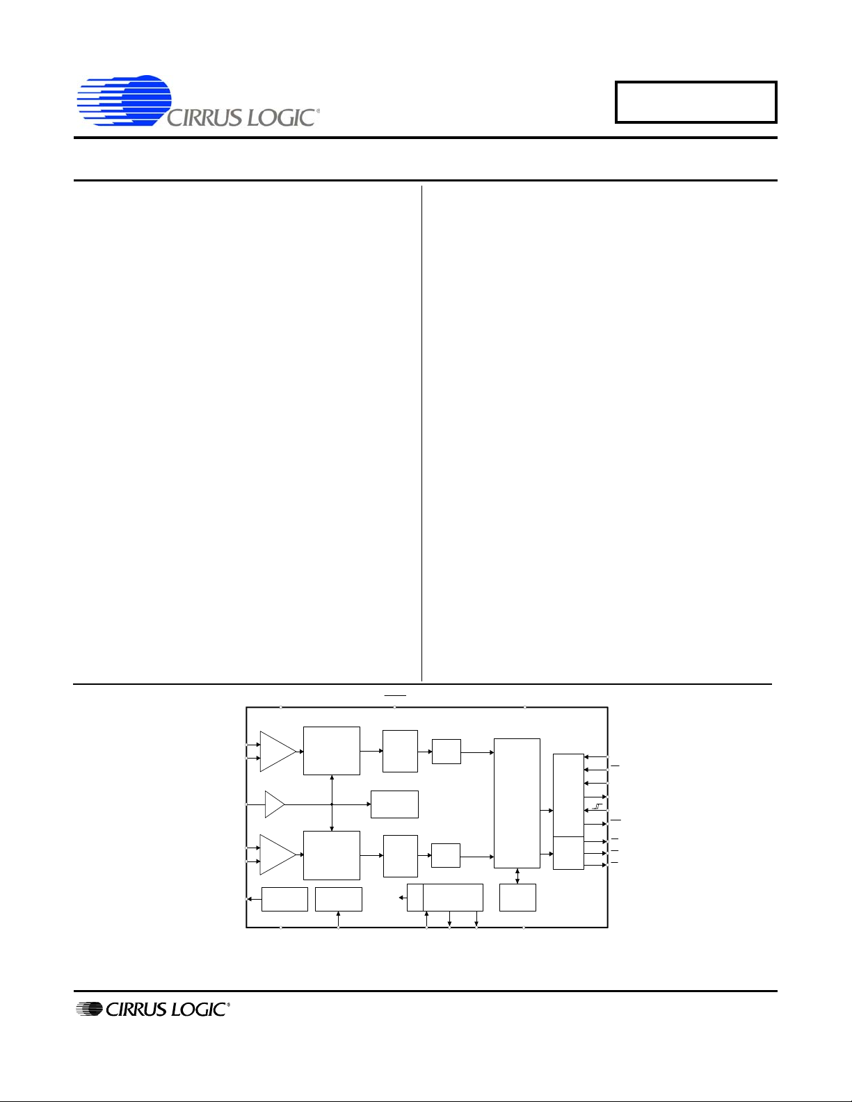
1. OVERVIEW
The CS5463 is a CMOS monolithic power measurement device with a computation engine and an energy-to-frequency pulse output. The CS5463 combines a programmable gain amplifier, two Analog-to-Digital Converters (ADCs), system calibration, and a computation engine on a single chip.
The CS5463 is designed for power measurement applications and is optimized to interface to a current
sense resistor or transformer for current measurement, and to a resistive divider or potential transformer
for voltage measurement. The current channel provides programmable gains to accommodate various input levels from a multitude of sensing elements. With single +5 V supply on VA+/AGND, both of the
CS5463’s input channels can accommodate common mode plus signal levels between (AGND - 0.25 V)
and VA+.
The CS5463 also is equipped with a computation engine that calculates instantaneous power, I
V
, apparent power, active (real) power, reactive power, harmonic active power, active and reactive
RMS
fundamental power, and power factor. The CS5463 additional features include line frequ ency, current and
voltage sag detection, zero-cross detection, positive-only accumulation mode, and three programmable
pulse output pins. To facilitate communication to a microprocessor, the CS5463 includes a simple
three-wire serial interface which is SPI™ and Microwire™ compatible. The CS5463 provides three outputs for energy registration. E1
, E2, and E3 are designed to interface to a microprocessor.
RMS
,
DS678F3 5
Page 6
CS5463
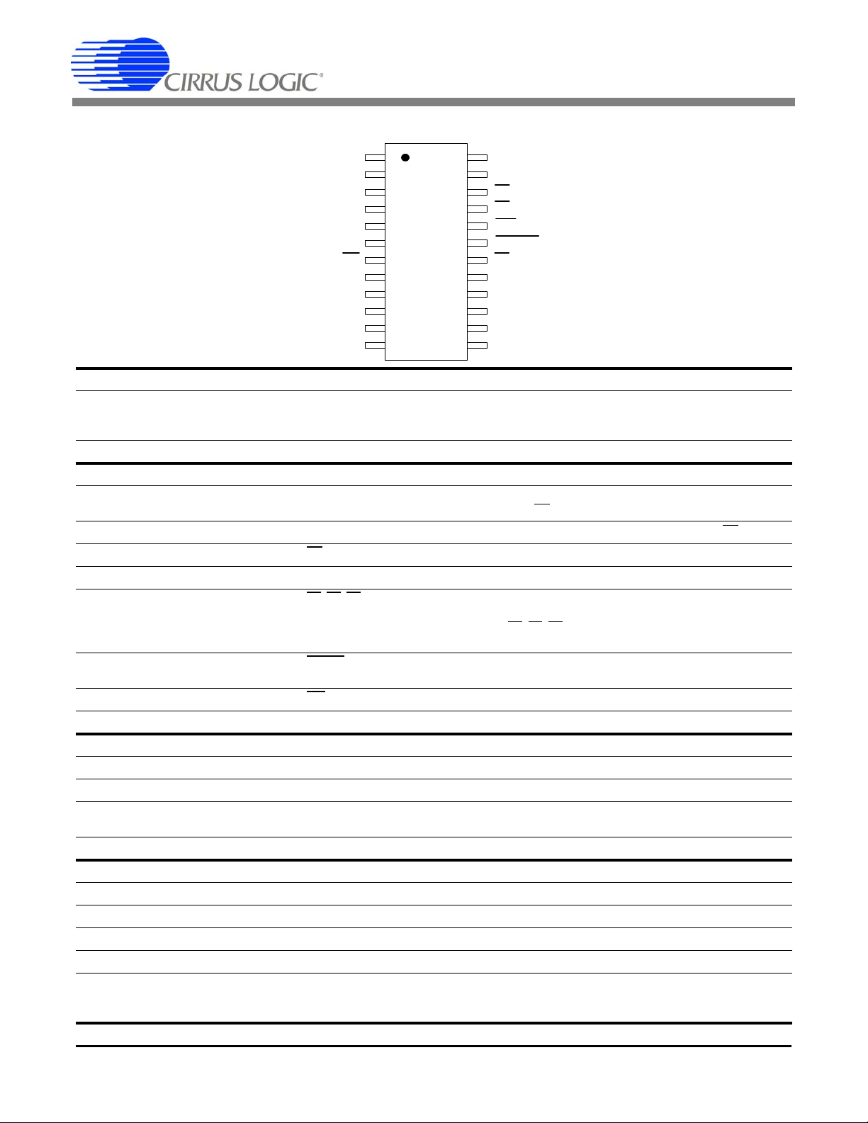
12
11
10
9
8
7
6
5
4
3
2
1
13
14
15
16
17
18
19
20
21
22
23
24
AGND Analog Ground
VA+ Positive Analog Supply
IIN- Differential Current Input
IIN+ Differential Current Input
PFMON Power Fail Monitor
E3 High Frequency Energy Output
RESET Reset
INT Interrupt
E1 Energy Output 1
SDI Serial D a t a Input
XIN Crysta l In
E2
Energy Output 2
VREFINVoltage Reference Input
VREFOUTVoltage Reference Output
VIN-Differential Voltage Input
VIN+Differential Voltage Input
MODEMode Select
CSChip Select
SDOSerial Data Ouput
SCLKSerial Clock
DGNDDigital Ground
VD+Positiv e Digita l Supp ly
CPUCLKCPU Clock Output
XOUTCrystal Out
2. PIN DESCRIPTION
Clock Generator
Crystal Out
1,24
Crystal In
CPU Clock Output 2
Control Pins and Serial Data I/O
Serial Clock Input 5
Serial Data Output 6
Chip Select 7
Mode Select 8
Energy Output 18,21,22
Reset 19
Interrupt 20
Serial Data Input 23
Analog Inputs/Outputs
Differential V ol tage Inputs 9,10
Differential Current Inputs 15,16
Voltage Reference Output 11
Voltage Reference Input 12
Power Supply Connections
Positive Digital Supply 3
Digital Ground 4
Positive Analog Supply 14
Analog Ground 13
Power Fail Monitor
6 DS678F3
XOUT, XIN – The output and input of an inverting amplifier. Oscillation occurs when connected to
a crystal, providing an on-chip system clock. Alternatively, an external clock can be supplied to
the XIN pin to provide the system clock for the device.
CPUCLK – Output of on-chip oscillator which can drive one standard CMOS load.
SCLK – A Schmitt-trigger input pin. Clocks data from the SDI pin into the receive buffer and out
of the transmit buffer onto the SDO pin when CS
SDO – Serial port data output pin.SDO is forced into a high-impedance state when CS is high.
CS – Low, activates the serial port interface.
MODE - High, enables the “auto-boot” mode. The mode pin has an internal pull-down resistor.
E3, E1, E2 – Active-low pulses with an output frequency proportional to the selected power. Con-
figurable outputs for active, apparent, and reactive power, negative energy indication, zero cross
detection, and power failure monitoring. E1
Modes Register.
RESET – A Schmitt-trigger input pin. Low activates Reset, all internal registers (some of which
drive output pins) are set to their default states.
INT - Low, indicates that an enabled event has occurred.
SDI - Serial port data input pin. Data will be input at a rate determined by SCLK.
VIN+, VIN- – Differential analog input pins for the voltage channel.
IIN+, IIN- – Differential analog input pins for the current channel.
VREFOUT – The on-chip voltage reference output. The voltage reference has a nominal magni-
tude of 2.5 V and is referenced to the AGND pin on the converter.
VREFIN – The input to this pin establishes the voltage reference for the on-chip modulator.
VD+ – The positive digital supply.
DGND – Digital Ground.
VA+ – The positive analog supply.
AGND – Analog ground.
PFMON – The power fail monitor pin monitors the analog supply. If the analog supply does not
17
meet or falls below PFMON’s voltage threshold, a Low-supply Detect (LSD) event is set in the
status register.
is low.
, E2, E3 outputs are configured in the Operational
Page 7
CS5463
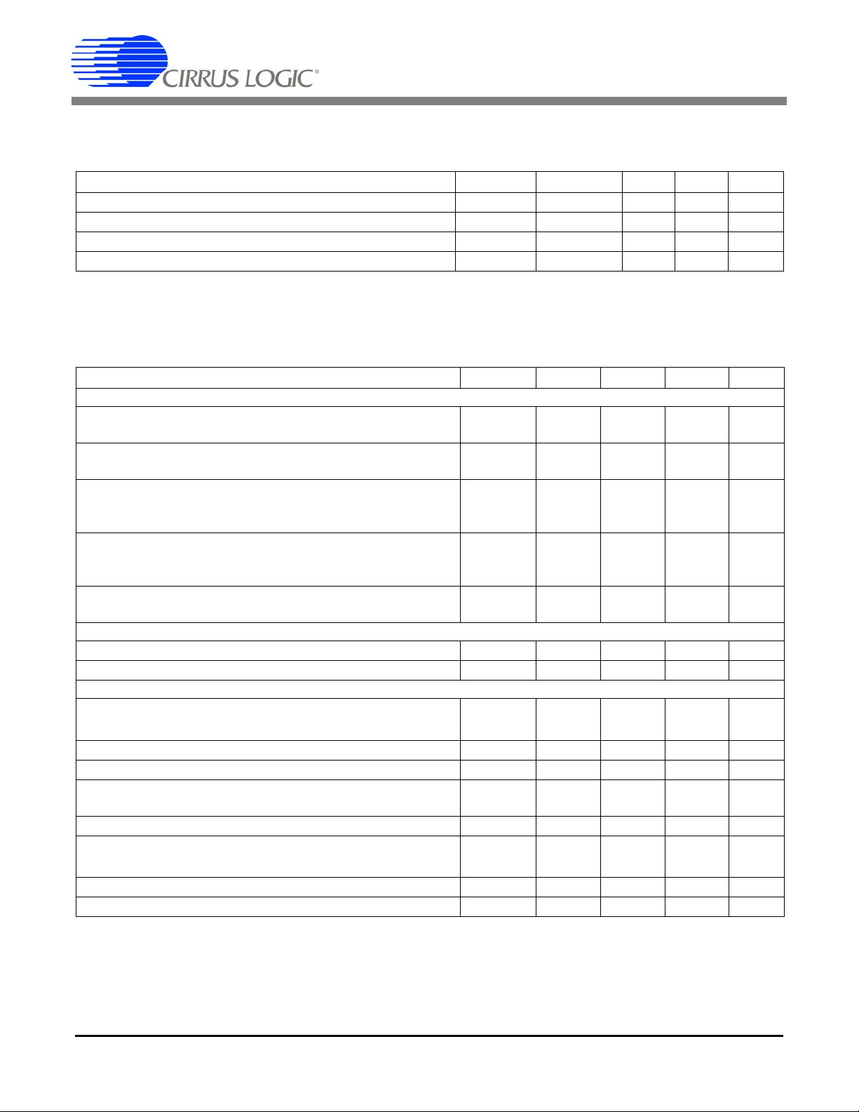
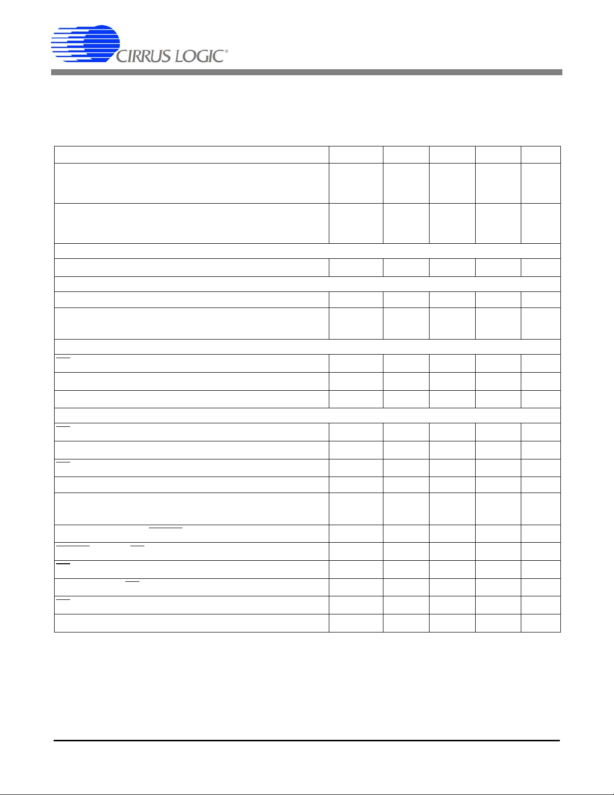
3. CHARACTERISTICS & SPECIFICATIONS
RECOMMENDED OPERATING CONDITIONS
Parameter Symbol Min Typ Max Unit
Positive Digital Power Supply VD+ 3.135 5.0 5.25 V
Positive Analog Power Supply VA+ 4.75 5.0 5.25 V
Voltage Reference VREFIN - 2.5 - V
Specified Temperature Range T
A
ANALOG CHARACTERISTICS
• Min / Max characteristics and specifications are guaranteed over all Recommended Operating Conditions.
• Typical characteristics and specifications are measured at nominal supply voltages and TA = 25 °C.
• VA+ = VD+ = 5 V ±5%; AGND = DGND = 0 V; VREFIN = +2.5V. All voltages with respect to 0 V.
• MCLK = 4.096 MHz.
Parameter Symbol Min Typ Max Unit
Accuracy
Active Power All Gain Ranges
(Note 1) Input Range 0.1% - 100%
Average Reactive Power All Gain Ranges
(Note 1 and 2) Input Range 0.1% - 100%
Power Factor All Gain Ranges
(Note 1 and 2) Input Range 1.0% - 100%
Input Range 0.1% - 1.0%
Current RMS All Gain Ranges
(Note 1) Input Range 0.2% - 100%
Input Range 0.1% - 0.2%
Voltage RMS All Gain Ranges
(Note 1) Input Range 5% - 100%
Analog Inputs (Both Channels)
Common Mode Rejection (DC, 50, 60 Hz) CMRR 80 - - dB
Common Mode + Signal All Gain Ranges -0.25 - VA+ V
Analog Inputs (Current Channel)
Differential Input Range (Gain = 10)
[(IIN+) - (IIN-)] (Gain = 50)
Total Harmonic Distortion (Gain = 50) THD 80 94 - dB
Crosstalk with Voltage Channel at Full Scale (50, 60 Hz) - -115 - dB
Input Capacitance (Gain = 10)
(Gain = 50)
Effective Input Impedance EII 30 - - k
Noise (Referred to Input) (Gain = 10)
(Gain = 50)
Offset Drift (Without the High Pass Filter) OD - 4.0 - µV/°C
Gain Error (Note 3) GE - ±0.4 %
Notes: 1. Applies when the HPF option is enabled.
2. Applies when the line frequency is equal to the product of the Output Word Rate (OWR) and the value
of epsilon (
).
P
Active
Q
Avg
PF -
I
RMS
V
RMS
IIN
IC
N
I
-40 - +85 °C
-±0.1-%
-±0.2-%
±0.2
-
±0.27
-
-
%
%
%
-
-
±0.2
±1.5
-
-
%
%
-±0.1-%
-
-
-
-
-
-
500
100
32
52
22.5
4.5
-
-
-
-
-
-
mV
mV
µV
µV
P-P
P-P
pF
pF
rms
rms
DS678F3 7
Page 8
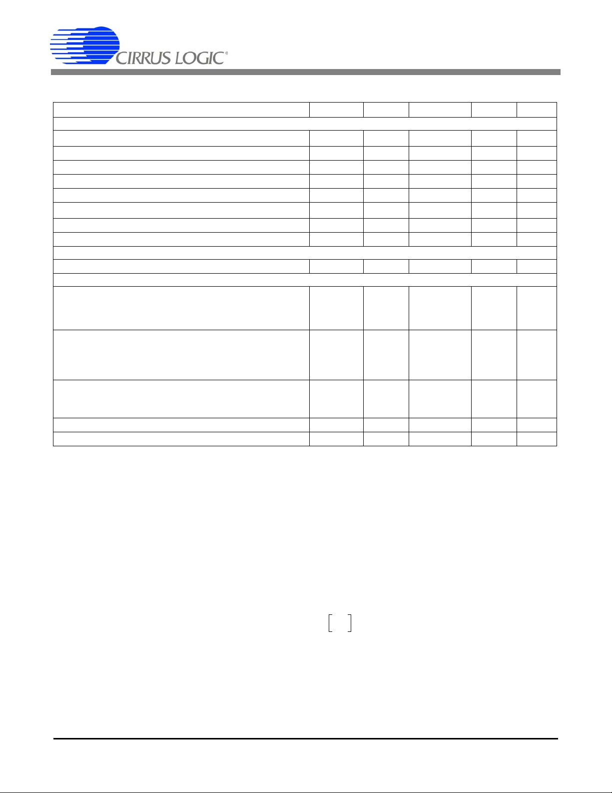
CS5463
PSRR 20
150
V
eq
--------- -
log=
ANALOG CHARACTERISTICS (Continued)
Parameter Symbol Min Typ Max Unit
Analog Inputs (Voltage Channel)
Differential Input Range [(VIN+) - (VIN-)] VIN - 500 - mV
Total Harmonic Distortion THD 65 75 - dB
Crosstalk with Current Channel at Full Scale (50, 60 Hz) - -70 - dB
Input Capacitance All Gain Ranges IC - 0.2 - pF
Effective Input Impedance EII 2 - - M
Noise (Referred to Input) N
V
-140-µV
Offset Drift (Without the High Pass Filter) OD - 16.0 - µV/°C
Gain Error (Note 3) GE - ±3.0 %
Temperature Channel
Temperature Accuracy T - ±5 - °C
Power Supplies
Power Supply Currents (Active State) I
I
(VA+ = VD+ = 5 V)
D+
(VA+ = 5 V, VD+ = 3.3 V)
I
D+
Power Consumption Active State (VA+ = VD+ = 5 V)
(Note 4) Active State (VA+ = 5 V, VD+ = 3.3 V)
St and-by State
Sleep State
Power Supply Rejection Ratio (50, 60 Hz)
(Note 5) Voltage Channel
Current Channel
PSCA
A+
PSCD
PSCD
PC -
PSRR 45
70
-
-
-
-
-
-
1.1
2.9
1.7
21
11.6
8
10
65
75
-
-
-
29
17.5
-
-
-
-
PFMON Low-voltage Tr igger Threshold (Note 6) PMLO 2.3 2.45 - V
PFMON High-voltage Power-on Trip Point (Note 7) PMHI - 2.55 2.7 V
Notes: 3. Applies before system calibration.
4. All outputs unloaded. All inputs CMOS level.
5. Measurement method for PSRR: VREFIN tied to VREFOUT, VA+ = VD+ = 5 V, a 150 mV
(zero-to-peak) (60 Hz) sinewave is imposed onto the +5 V DC supply voltage at VA+ and VD+ pins. The
“+” and “-” input pins of both input ch annels a re sh or ted to AGND. T hen the CS5 463 is command ed to
continuous conversion acquisition mode, and digital output data is collected for the chan nel under test.
The (zero-to-peak) value of the digital sinusoidal out put signal is determined, and this value is converted
into the (zero-to-peak) value of the sinusoidal voltage (me asured in m V) that would need to be applied
at the channel’s inputs, in order to cause the sa me digital sinusoidal output. This voltage is then defined
as Veq. PSRR is then (in dB)
:
P-P
rms
mA
mA
mA
mW
mW
mW
µW
dB
dB
6. When voltage level on PFMON is sagging, and LSD bit = 0, the voltage at which LSD is set to 1.
7. If the LSD bit has been set to 1 (because PFMON voltage fell below PMLO), this is the voltage level on
PFMON at which the LSD bit can be permanently reset back to 0.
8 DS678F3
Page 9

CS5463
(VREFOUTMAX - VREFOUTMIN)
VREFOUT
AVG
(
(
1
T
A
MAX
- T
A
MIN
(
(
1.0 x 10
(
(
6
TC
VREF
=
VOLTAGE REFERENCE
Parameter Symbol Min Typ Max Unit
Reference Output
Output Voltage VREFOUT +2.4 +2.5 +2.6 V
Temperature Coefficient (Note 8) TC
Load Regulation (Note 9) V
Reference Input
VREF
R
Input Voltage Range VREFIN +2.4 +2.5 +2.6 V
Input Capacitance - 4 - pF
Input CVF Current - 25 - nA
Notes: 8. The voltage at VREFOUT is measured across the temperature range. From these measurements the
following formula is used to calculate the VREFOUT Temperature Coefficient:.
9. Specified at maximum recommended output of 1 µA, source or sink.
DIGITAL CHARACTERISTICS
• Min / Max characteristics and specifications are guaranteed over all Recommended Operating Conditions.
• Typical characteristics and specifications are measured at nominal supply voltages and TA = 25 °C.
• VA+ = VD+ = 5V ±5%; AGND = DGND = 0 V. All voltages with respect to 0 V.
• MCLK = 4.096 MHz.
- 25 60 ppm/°C
-610mV
Parameter Symbol Min Typ Max Unit
Master Clock Characteristics
Master Clock Frequency Internal Gate Oscillator (Note 11) MCLK 2.5 4.096 2 0 MHz
Master Clock Duty Cycle 40 - 60 %
CPUCLK Duty Cycle (Note 12 and 13) 40 - 60 %
Filter Characteristics
Phase Compensation Range (Voltage Channel, 60 Hz) -2.8 - +2.8 °
Input Sampling Rate DCLK = MCLK/K - DCLK/8 - Hz
Digital Filter Output Word Rate (Both Channels) OWR - DCLK/1024 - Hz
High-pass Filter Corner Frequency -3 dB - 0.5 - Hz
Full-scale DC Calibration Range (
Referred to Input) (Note 14) FSCR 25 - 100 %F.S.
Channel-to-channel Time-shift Error (Note 15) 1.0 µs
Input/Output Characteristics
High-level Input Voltage
All Pins Except XIN and SCLK and RESET
XIN
SCLK and RESET
Low-level Input Voltage (VD = 5 V)
All Pins Except XIN and SCLK and RESET
XIN
SCLK and RESET
V
IH
V
IL
0.6 VD+
(VD+) - 0.5
0.8VD+
-
-
-
-
-
-
-
-
-
-
-
-
0.8
1.5
0.2VD+
V
V
V
V
V
V
DS678F3 9
Page 10

Parameter Symbol Min Typ Max Unit
Low-level Input Voltage (VD = 3.3 V)
All Pins Except XIN and SCLK and RESET
XIN
SCLK and RESET
High-level Output Voltage I
Low-level Output Voltage I
= +5 mA V
out
= -5 mA V
out
Input Leakage Current (Note 16) I
3-state Leakage Current I
Digital Output Pin Capacitance C
Notes: 10. All measurements performed under static conditions.
11. If a crystal is used, then XIN frequency must remain between 2.5 MHz - 5.0 MHz. If an external
oscillator is used, XIN frequency range is 2.5 MHz - 20 MHz, but K must be set so that MCLK is between
2.5 MHz - 5.0 MHz.
12. If ex ternal MC LK is used, then the duty cycle must be between 45% and 55% to maintain this
specification.
13. The frequency of CPUCLK is equal to MCLK.
14. The minimum FSCR is limited by the maximum allowed gain register value. The maximum FSCR is
limited by the full-scale signal applied to the channel input.
15. Configuration Register bits PC[6:0] are set to “0000000”.
16. The MODE pin is pulled low by an internal resistor.
V
IL
OH
OL
in
OZ
out
-
-
-
-
-
-
(VD+) - 1.0 - - V
--0.4V
-±1±10µA
--±10µA
-5-pF
CS5463
0.48
0.3
0.2VD+
V
V
V
10 DS678F3
Page 11
CS5463
SWITCHING CHARACTERISTICS
• Min / Max characteristics and specifications are guaranteed over all Recommended Operating Conditions.
• Typical characteristics and specifications are measured at nominal supply voltages and TA = 25 °C.
• VA+ = 5 V ±5% VD+ = 3.3 V ±5% or 5 V ±5%; AGND = DGND = 0 V. All voltages with respect to 0 V.
• Logic Levels: Logic 0 = 0 V, Logic 1 = VD+.
Parameter Symbol Min Typ Max Unit
Rise Times Any Digital Input Except SCLK
(Note 17) SCLK
Any Digital Output
Fall Times Any Digital Input Except SCLK
(Note 17) SCLK
Any Digital Output
Start-up
Oscillator Start-up Time XTAL = 4.096 MHz (Note 18) t
Serial Port Timing
Serial Clock Frequency SCLK - - 2 MHz
Serial Clock Pulse Width High
Pulse Width Low
SDI Timing
CS Falling to SCLK Rising t
Data Set-up Time Prior to SCLK Rising t
Data Hold Time After SCLK Rising t
SDO Timing
CS Falling to SDI Driving t
SCLK Falling to New Data Bit (hold time) t
Rising to SDO Hi-Z t
CS
Auto-Boot Timing
Serial Clock Pulse Width Low
Pulse Width High
MODE setup time to RESET
RESET
CS
SCLK falling to CS
CS
rising to CS falling t
falling to SCLK rising t
rising t
rising to driving MODE low (to end auto-boot sequence) t
Rising t
SDO guaranteed setup time to SCLK rising t
Notes: 17. Specified using 10% and 90% points on waveform of interest. Output loaded with 50 pF.
18. Oscillator start-up time varies with crystal parameters. This specification does not apply when using an
external clock source.
t
t
t
rise
fall
ost
t
1
t
2
3
4
5
6
7
8
t
9
10
11
12
13
14
15
16
-
-
-
-
-
-
50
50
-
-
-
-
1.0
100
-
1.0
100
-
µs
µs
ns
µs
µs
ns
-60-ms
200
200
-
-
-
-
ns
ns
50 - - ns
50 - - ns
100 - - ns
-2050ns
-2050ns
-2050ns
8
8
MCLK
MCLK
50 ns
48 MCLK
100 8 MCLK
16 MCLK
50 ns
100 ns
DS678F3 11
Page 12
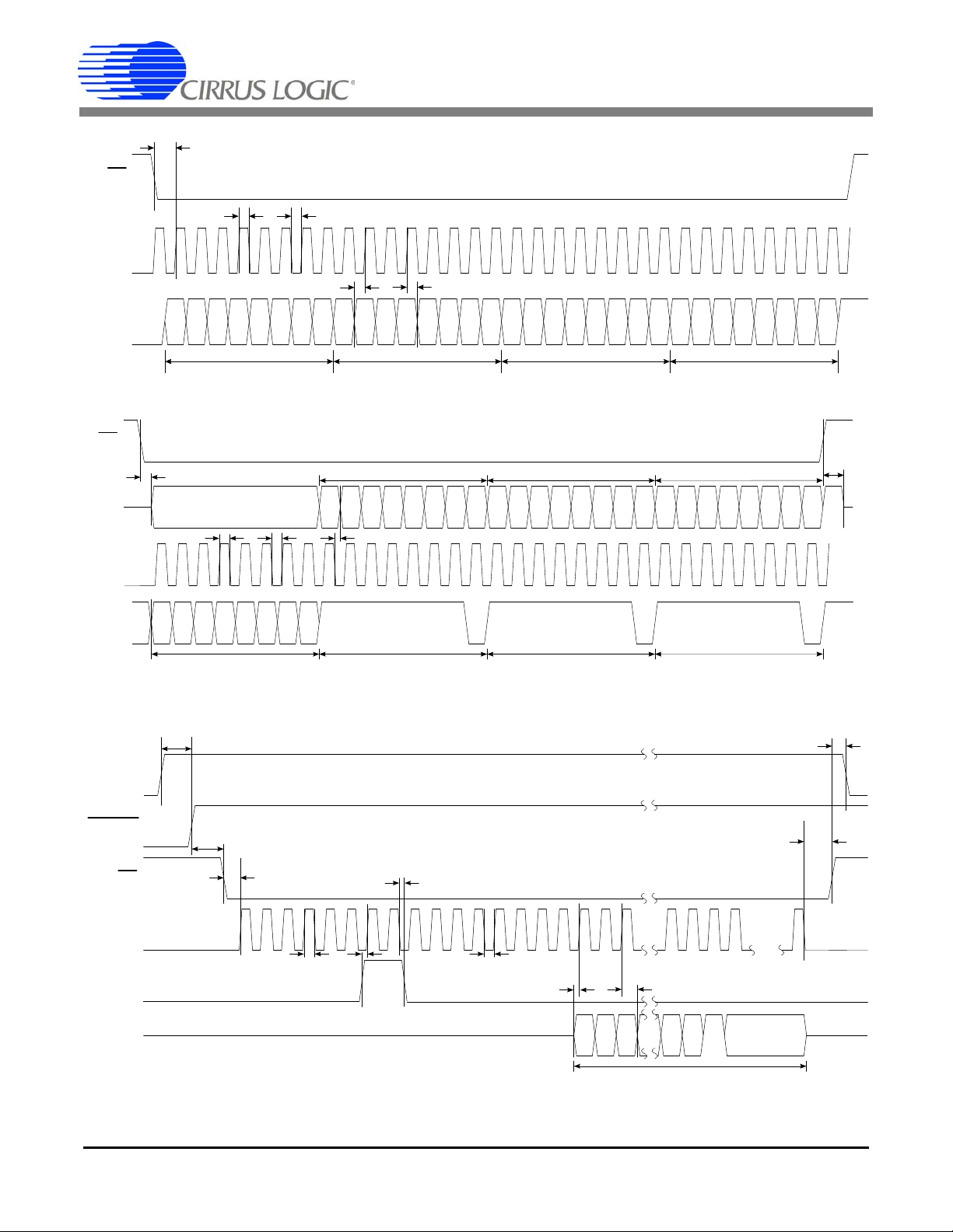
t
1
t
2
t
3
t
4
t
5
MSB
MSB-1
LSB
MSB
MSB-1
LSB
MSB
MSB-1
LSB
MSB
MSB-1
LSB
Com m and Tim e 8 SC LKs High Byte M id Byte Low Byte
CS
SCLK
SDI
t
10
t
9
RESET
SDO
SCLK
CS
Last 8
Bits
SDI
MODE
STOP bit
D a ta fro m E E P R O M
t
16
t
4
t
5
t
14
t
15
t
7
t
13
t
12
t
11
(INPUT)
(INPUT)
(O UT P U T )
(O UT P U T )
(O UT P U T )
(INPUT)
SDI Write Timing (Not to Scale)
SDO Read Timing (Not to Scale)
Figure 1. CS5463 Read and Write Timing Diagrams
Auto-boot Sequence Timing (Not to Scale)
t
1
t
2
MSB
MSB-1
LSB
Com m and Time 8 SC LKs
SYNC0 or SYNC1
Com mand
SYN C 0 or SYN C1
Command
MSB
MSB-1
LSB
MSB
MSB-1
LSB
MSB
MSB-1
LSB
H igh B y te M id B y te Low By te
CS
SDO
SDI
t
6
t
7
t
8
SYNC0 or SYNC1
Command
UNKNOWN
CS5463
12 DS678F3
Page 13
CS5463
t
period
E1
t
3
t
4
t
5
t
3
t
5
t
4
E2
E3
t
pw
t
period
t
pw
Figure 2. Timing Diagram for E1, E2, and E3
SWITCHING CHARACTERISTICS (Continued)
Parameter Symbol Min Typ Max Unit
E1
, E2, and E3 Timing (Note 19 and 20)
Period t
Pulse Width t
Rising Edge to Falling Edge t
Setup to E1 and/or E3 Falling Edge t
E2
Falling Edge to E3 Falling Edge t
E1
period
pw
3
4
5
Notes: 19. Pulse output timing is specified at MCLK = 4.096 MHz, E2MODE = 0, and E3MODE[1:0] = 0. Refer to
Section 5.5 Energy Pulse Output on page 17 for more information on pulse output pins.
20. Timing is proportional to the frequency of MCLK.
250 - - s
244 - - s
6--s
1.5 - - s
248 - - s
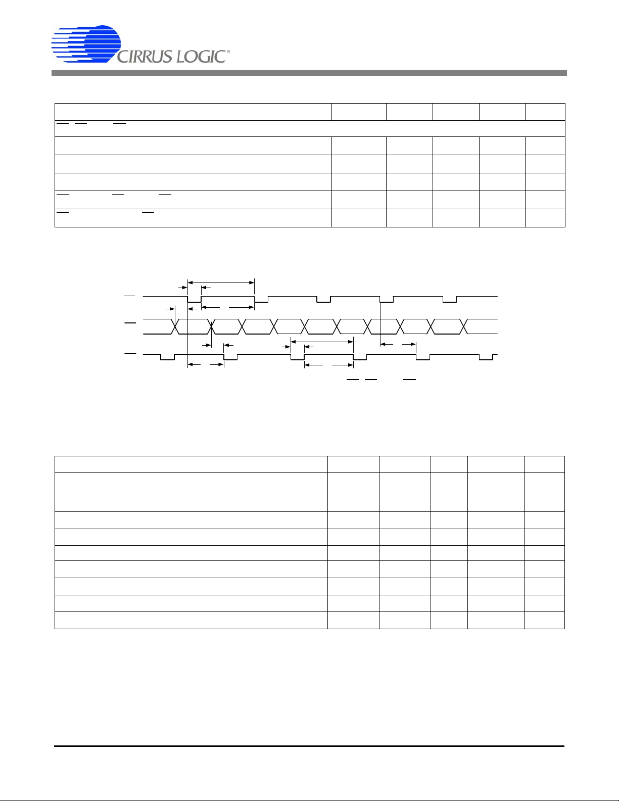
ABSOLUTE MAXIMUM RATINGS
WARNING: Operation at or beyond these limits may result in permanent damage to the device.
Normal operation is not guaranteed at these extremes
Parameter Symbol Min Typ Max Unit
DC Power Supplies (Notes 21 and 22)
Positive Digital
Positive Analog
Input Current, Any Pin Except Supplies (Notes 23, 24, 25) I
Output Current, Any Pin Except VREFOUT I
Power Dissipation (Note 26) P
Analog Input Voltage All Analog Pins V
Digital Input Voltage All Digital Pins V
Ambient Operating Temperature T
Storage Temperature T
Notes: 21. VA+ and AGND must satisfy [(VA+) - (AGND)] + 6.0 V.
22. VD+ and AGND must satisfy [(VD+) - (AGND)] + 6.0 V.
23. Applies to all pins including continuous over-voltage conditions at the analog input pins.
24. Transient current of up to 100 mA will not cause SCR latch-up.
25. Maximum DC input current for a power supply pin is ±50 mA.
26. Total power dissipation, including all input currents and output currents.
.
VD+
VA+
IN
OUT
D --500mW
INA
IND
A
stg
-0.3
-0.3
--±10mA
--100mA
- 0.3 - (VA+) + 0.3 V
-0.3 - (VD+) + 0.3 V
-40 - 85 °C
-65 - 150 °C
-
-
+6.0
+6.0
V
V
DS678F3 13
Page 14
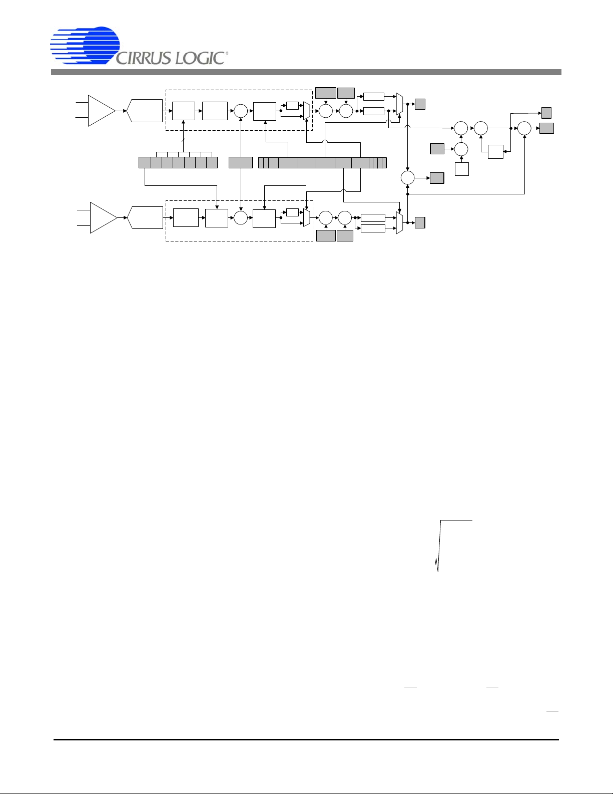
4. THEORY OF OPERATION
VOLTAGE
SINC
3
+
X
V*
gn
CURRENT
SINC
3
+
X
I*
gn
DELAY
REG
DELAY
REG
I
DCoff
*
V
DCoff
*
PGA
+
+
Configuration Register *
Digital Filter
Digital Filter
HPF
2nd Order
Modulator
4th Order
Modulator
x10
X
X
SYS
Gain
*
PC6 PC5 PC4 PC3
PC2
PC1 PC0
6
*
DENOTES REGISTER NAME.
DELAY
REG
DELAY
REG
HPF
V
Q
*
XVDEL XIDEL
012
2322
87
...
Operational Modes Register *
+
X
+
X
X
Q
*
2
MUX
X
V
*
P
*
I
*
MUX
VHPF IHPF
65
*
APF
HPF
APF
MUX
IIR
MUX
IIR
3
IIR
4
Figure 3. Data Measurement Flow Diagram.
I
RMS
I
n
n0=
N1–
N
-------------------- -
=
The CS5463 is a dual-channel analog-to-digital converter (ADC) followed by a computation engine that performs power calculations and energy-to-pulse
conversion. The data flow for the voltage and current
channel measurement and the power calculation algorithms are depicted in Figure 3 and 4, respectively.
The analog inputs are structured with two dedicated
channels,
fy interfacing to various sensing elements.
The voltage-sensing element introduces a voltage
waveform on the voltage channel input VIN± and is subject to a gain of 10x. A second-order delta-sigma modulator samples the amplified signal for digitization.
Simultaneously, the current-sensing element introduces
a voltage waveform on the current channel input IIN±
and is subject to two selectable gains of the programmable gain amplifier (PGA). The amplified signal is
sampled by a fourth-order delta-sigma modulator for
digitization. Both converters sample at a rate of
MCLK /8, the over-sampling provides a wide dynamic
range and simplified anti-alias filter design.
Voltage and Current, then optimized to simpli-
CS5463
from the calculated V
RMS
and I
ent power.
When the optional HPF in either channel is disabled, an
all-pass filter (APF) is implemented. The APF has an
amplitude response that is flat within the channel bandwidth and is used for matching phase in systems where
only one HPF is engaged.
4.2 Voltage and Current Measurements
The digital filter output word is then subject to a DC offset adjustment and a gain calibration (See Section 7.
System Calibration on page 37). The calibrated me a-
surement is available by reading the instantaneous voltage and current registers.
The Root Mean Square (
are performed on N instantaneous voltage and current
samples, V
n and In, respectively (where N is the cycle
count), using the formula:
RMS in Figure 4) calculations
as well as the appar-
RMS
4.1 Digital Filters
3
and likewise for V
, using Vn. I
RMS
RMS
and V
cessible by register reads, which are updated once every cycle count (referred to as a computational cycle).
4.3 Power Measurements
The instantaneous voltage and current samples are
multiplied to obtain the instantaneous power (see Figure 3). The product is then averaged over N conversions to compute active power and is used to drive
energy pulse output E1
providing an energy sign or a pulse output that is proportional to the apparent power. Energy output E3
. Energy output E2 is selectable,
RMS
The decimating digital filters on both channels a re Sinc
filters followed by 4th-order IIR filters. The single-bit
data is passed to the low-pass decimation filter and output at a fixed word rate. The output word is passed to an
optional IIR filter to compensate for the magnitude roll
off of the low-pass filtering operation.
An optional digital high-pass filter (
moves any DC component from the selected signal
HPF in Figure 3) re-
path. By removing the DC component from the voltage
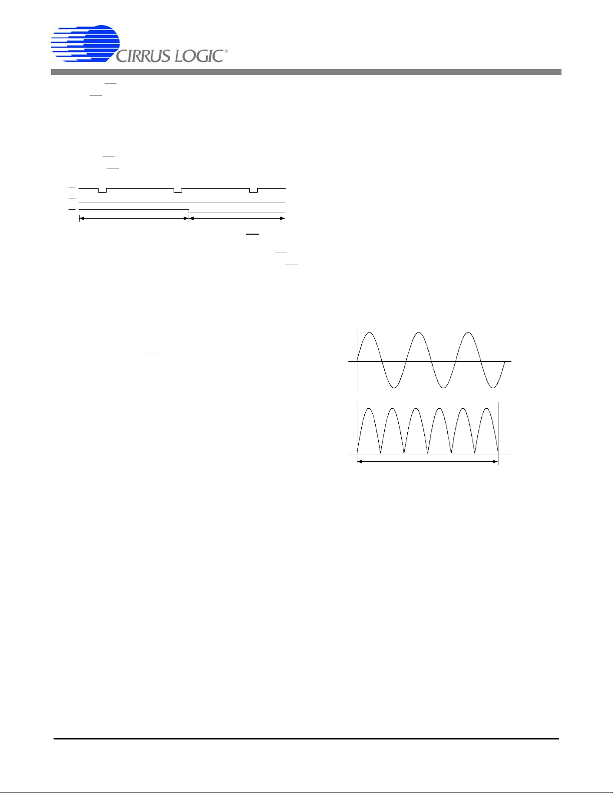
and/or the current channel, any DC content will also be
removed from the calculated active power as well. With
both HPFs enabled the DC component will be removed
14 DS678F3
are ac-
Page 15

CS5463
X
V
*
I*
RMS
V*
RMS
E1
I
*
Energy-to-pulseX
E3
+
+
X
+
I
ACoff
*
+
+
V
ACoff
*
+
E2
N
÷
N
N
÷
N
P
*
ACTIVE
N
÷
N
P
off
*
P
*
PulseRate
*
*
DENOTES REGISTER NAM E.
X
S
*
Q
*
AVG
-
+
X
Invers e
X
PF
*
Q
TRIG
*
Q
*
N
÷
N
X
Figure 4. Power Calculation Flow.
SV
RMSIRMS
=
PF
P
Active
S
------------------
=
Q
Trig
S2P
Active
2
–=
Q
Avg
Q
n
n1=
N
N
------------------------ -
=
provides a pulse output that is proportional to the reactive power or apparent power. Output E3
can also be set
quadrature power (Q). The product is then averaged
over N conversions, utilizing the formula
to display the sign of the voltage applied to the voltage
channel or the PFMON comparator output.
The apparent power (S) is the combination of the active
power and reactive power, without reference to an impedance phase angle, and is calculated by the CS5463
using the following formula:
Fundamental active (P
culated by performing a discrete Fourier transform
) and reactive (QF) power is cal-
F
(DFT) at the relevant frequency on the instantaneous
voltage (V) and current (I). Epsilon is used to set the fre-
quency of the internal sine (imaginary component) and
cosine (real component) waveform generator. The harPower Factor (PF) is the active power (P
by the apparent power (S)
Active
) divided
monic active power (P
fundamental active power (P
(P
Active
).
The peak current (I
) is calculated by subtracting the
H
) and peak voltage (V
peak
) from the active power
F
peak
) are
the instantaneous current and voltage, respectively,
with the greatest magnitude detected during the last
computation cycle. Active, apparent, reactive, and fun-
The sign of the power factor is determined by the a ctive
damental power are updated every computation cycle.
power.
4.4 Linearity Performance
The CS5463 calculates the reactive power, Q
ing trigonometric identities, giving the formula
Average reactive power, Q
ing the voltage multiplied by the current with a 90°
shift difference between them. The 90° phase shift is realized by applying an IIR digital filter in the voltage channel to obtain quadrature voltage (see Figure 3). This
filter will give exactly -90° phase shift across all frequencies, and utilizes epsilon (
line frequency.
The instantaneous quadrature voltage (V
(I) samples are multiplied to obtain the instantaneous
DS678F3 15
, is generated by averag-
Avg
) to achieve unity gain at the
Q
utiliz-
Trig
phase
) and current
The linearity of the V
RMS
, I
, active, reactive, and
RMS
power-factor power measurements (before calibration)
will be within ±0.1% of reading over the ranges specified, with respect to the input voltage levels required to
cause full-scale readings in the I
ters. Refer to
Accuracy Specifications on page 7.
Until the CS5463 is calibrated, the
and V
RMS
accuracy of the
RMS
CS5463 (with respect to a reference line-voltage and
line-current level on the power mains) is not guaranteed
to within ±0.1%. (See Section 7.
page 37.) The accuracy of the internal calculations can
often be improved by selecting a value for the Cycle
Count Register that will cause the time duration of one
computation cycle to be equal to (or very close to) a
System Calibration on
whole number of power-line cycles (and N must be
greater than or equal to 4000).
regis-
Page 16

5. FUNCTIONAL DESCRIPTION
250mV
P
2
---------------------
176.78mV
RMS
OWR
MCLK K
1024
-----------------------------
=
Computation Cycle
OWR
N
---------------
=
CS5463
5.1 Analog Inputs
The CS5463 is equipped with two fully differential input
channels. The inputs VIN
and IIN are designated as
the voltage and current channel inputs, respectively.
The full-scale differential input voltage for the current
and voltage channel is
250 mV
.
P
5.1.1 Voltage Channel
The output of the line voltage resistive divider or transformer is connected to the VIN+ and VIN- input pins of
the CS5463. The voltage channel is equipped with a
10x fixed-gain amplifier. The full-scale signal level that
can be applied to the voltage channel is
250 mV. If the
input signal is a sine wave the maximum RMS voltage
at a gain 10x is:
which is approximately 70.7% of maximum peak voltage. The voltage channel is also equipped with a
age Gain Register
, allowing for an additional
Volt-
programmable gain of up to 4x.
5.1.2 Current Channel
The output of the current-sense resistor or transformer
is connected to the IIN+ and IIN- input pins of the
CS5463. To accommodate different current sensing elements the current channel incorporates a prog rammable gain amplifier (PGA) with two programmable input
Configuration Register bit Igain (see Table 1) de-
gains.
fines the two gain selections and corresponding maximum input-signal level.
Igain Maximum Input Range
0±250mV10x
1 ±50 mV 50x
Table 1. Current Channel PGA Setting
For example, if Igain=0, the current channel’s PGA gain
is set to 10x. If the input signals are pure sinusoids with
zero phase shift, the maximum peak differential signal
on the current or voltage channel is
250 mV
put signal levels are approximately 70.7% of maximum
peak voltage producing a full-scale energy pulse registration equal to 50% of absolute maximum energy pulse
registration. This will be discussed further in See Section 5.5
The
Energy Pulse Output on page 17.
Current Gain Register also facilitates an additional
programmable gain of up to 4x. If an addit ional gain is
. The in-
P
applied to the voltage and/or current channel, the maximum input range should be adjusted accordingly.
5.2 IIR Filters
The current and voltage channel are equipped with a
4th-order IIR filter, that is used to compensate for the
magnitude roll off of the low-pass decimation filter.
erational Mode Register
bit IIR engages the IIR filters in
Op-
both the voltage and current channels.
5.3 High-pass Filters
By removing the offset from either channel, no error
component will be generated at DC when computing the
active power. By removing the offset from both channels, no error component will be generated at DC when
, I
computing V
RMS
al Mode Register
, and apparent power. Operation-
RMS
bits VHPF and IHPF activate the HPF
in the voltage and current channel respectively. When a
high-pass filter is active in only one channel, an all-pass
filter (APF) is applied to the other channel. The APF has
an amplitude response that is flat within the channel
bandwidth and is used for ma tching phase in systems
where only one HPF is engaged.
5.4 Performing Measurements
The CS5463 performs measurements of instantaneous
voltage (V
neous power (P
where K is the clock divider selected in the
tion Register
The RMS voltage (V
tive power (P
samples of V
value in the
computation cycle”. The apparent power (S) is the
a “
product of V
rived from the master clock (MCLK), with frequency:
Under default conditions and with K = 1, N = 4000, and
MCLK = 4.096 MHz – the OWR = 4000 Hz and the
ComputationCycle= 1Hz.
All measurements are available as a percentage of full
scale. The format for
ment, normalized value between -1 and +1. The format
) and current (In), and calculates instanta-
n
) at an output word rate (OWR) of
n
Configura-
.
), RMS current (I
RMS
) are computed using N instantaneous
active
, In, and Pn respectively, where N is the
n
RMS
), and ac-
Cycle Count Register and is referred to as
RMS
and I
. A computation cycle is de-
RMS
signed registers is a two’s comple-
16 DS678F3
Page 17

CS5463
2231–
2
23
------------------------
0.99999988
=
f
ifs
=
50 Hz 4000 Hz 0.0125==
60 Hz 4000 Hz 0.015==
tpwsecPulseWidth
1
( MCLK/K ) / 1024
----------------------------------------------- -
E3
E2
E1
Figure 5. Active and Reactive energy pulse outputs
for unsigned registe rs is a norm alized value between 0
and 1. A register value of
represents the maximum possible value.
At each instantaneous measurement, the CRDY bit will
be set in the
come active if the CRDY bit is unmasked in the
Register
DRDY bit will be set in the
Status Register, and the INT pin will be-
Mask
. At the end of each computation cycle, the
Status Register, and the INT
pin will become active if the DRDY bit is unmasked in
Mask Register. When these bits are asserted, they
the
must be cleared before they can be asserted again.
Cycle Count Register (N) is set to 1, all output cal-
If the
culations are instantaneous, and DRDY, like CRDY, will
indicate when instantaneous measurements are finished. Some calculations are inhibited when the cycle
count is less than 2.
Epsilon (
the sample frequency (f
where f
) is the ratio of the input line frequency (f
) of the ADC.
s
= MCLK / (K*1024). With MCLK = 4.096 MHz
s
and clock divider K = 1, f
= 4000 Hz. For the two
s
) to
i
most-common line frequencies, 50 Hz and 60 Hz
the pulse output mode, which is controlled by bit
E2MODE in the
Operational Mode Register.
E2MODE E2 Output Mode
0 Sign of Energy
1 Apparent Energy
Table 2. E2 Pin Configuration
The E3 pin can be set to register Reactive Energy (default), PFMON, Voltage Channel Sign, or Apparent Energy. Table 3 defines the pulse output format, which is
controlled by bits E3MODE[1:0] in the
Operational
Mode Register.
E3MODE1 E3MODE0 E3
OutPut Mode
0 0 Reactive Energy
01 PFMON
1 0 Voltage Channel Sign
1 1 Apparent Energy
Table 3. E3 Pin Configuration
The pulse output frequency of E1, E2, and E3 is directly
proportional to the power calculated from the input signals. The value contained in the
PulseRateE Register is
the ratio of the frequency of energy-output pulses to the
number of samples, at full scale, which defines th e average frequency for the output pulses. The pulse width,
in Figure 2, is programmable through the Pulse-
t
pw
Width register, and is approximately equal to:
and
respectively. Epsilon is used to set the frequency of the
internal sine/cosine reference for the fundamental active and reactive measurements, and the gain of the 90°
phase shift (IIR) filter for the average reactive power.
5.5 Energy Pulse Output
The CS5463 provides three output pins for energy registration. By default, E1
isters reactive energy, and E2
active and reactive energy. (See Figure 2.
gram for E1, E2, and E3
put is designed to register the Active Energy. The E2
can be set to register Apparent En ergy. Tab le 2 de fines
DS678F3 17
registers active energy, E3 reg-
indicates the sign of both
on page13.) The E1 pulse out-
Timing Dia-
pin
If MCLK =
0.25 ms.
t
pw
4.096 MHz, K = 1, and PulseWidth = 1, then
5.5.1 Active Energy
The E1 pin produces active-low pulses with an output
frequency proportional to the active power. The E2
is the energy direction indicator. Positive energy is represented by E1
energy is represented by the E1
pin falling while the E2 is high. Negative
pin falling while the E2
is low. The E1 and E2 switching characteristics are
specified in Figure 2.
Timing Diagram for E1, E2, and E3
on page13.
Figure 5 illustrates the pulse output format with positive
active energy and negative reactive energy.
pin
Page 18

CS5463
FREQP = Average frequency of active energy E1 pulses [Hz]
VIN = rms voltage across VIN+ and VIN- [V]
VGAIN = Voltage channel gain
IIN = rms voltage across IIN+ and IIN- [V]
IGAIN = Current channel gain
PF = Power Factor
PulseRate = PulseRateE x (MCLK/K)/2048 [Hz]
VREFIN = Voltage at VREFIN pin [V]
FREQ
P
VIN VGA IN IIN IGAIN PF P ulseRate
VREFIN
2
---------------------------------------------------------------------------------------------------------------------------------=
E3
E2
E1
Figure 6. Apparent energy pulse outputs
FREQS = Average frequency of apparent energy E2 and/or E3 pulses [Hz]
VIN = rms voltage across VIN+ and VIN- [V]
VGAIN = Voltage channel gain
IIN = rms voltage across IIN+ and IIN- [V]
IGAIN = Current channel gain
PulseRate = PulseRateE x (MCLK/K)/2048 [Hz]
VREFIN = Voltage at VREFIN pin [V]
FREQ
S
VIN VGA IN IIN IGAIN PulseRate
VREFIN
2
------------------------------------------------------------------------------------------------------------------=
FREQQ = Average frequency of reactive energy E3 pulses [Hz]
VIN = rms voltage across VIN+ and VIN- [V]
VGAIN = Voltage channel gain
IIN = rms voltage across IIN+ and IIN- [V]
IGAIN = Current channel gain
PQ =
PulseRate = PulseRateE x (MCLK/K)/2048 [Hz]
VREFIN = Voltage at VREFIN pin [V]
FREQ
Q
VIN VGAIN IIN IGAIN PQ PulseRate
VREFIN
2
----------------------------------------------------------------------------------------------------------------------------------=
1PF2–
E3
E2
E1
Figure 7. Voltage Channel Sign Pulse outputs
The pulse output frequency of E1 is directly proportional
to the active power calculated from the input signals. To
calculate the output frequency of E1
, the following trans-
fer function can be utilized:
With MCLK = 4.096 MHz, PF = 1, and default settings,
the pulses will have an average frequency equal to the
frequency specified by
PulseRate when the input sig-
nals applied to the voltage and current channels cause
full-scale readings in the instantaneous voltage and current registers. The maximum pulse frequency from the
pin is (MCLK/K)/2048.
E1
5.5.2 Apparent Energy Mode
Pin E2 outputs apparent energy pulses when the Oper-
ational Mode Register
apparent energy pulses when the
Register
bits E3MODE[1:0] = 3 (11b). Figure 6 illus-
trates the pulse output format with apparent energy on
(E2MODE = 1 and E3MODE[1:0] = 0)
E2
bit E2MODE = 1. Pin E3 outputs
Operational Mode
With MCLK = 4.096 MHz and default settings, the pulses will have an average frequency equal to the frequency specified by
PulseRate when the input signals
applied to the voltage and current channels cause
full-scale readings in the instantaneous voltage and current registers. The maximum pulse frequency from the
(and/or E3) pin is (MCLK/K) /2048. The E2 (and/or
E2
) pin outputs apparent energy, but has no energy di-
E3
rection indicator.
5.5.3 Reactive Energy Mode
Reactive energy pulses are output on pin E3 by setting
bit E3MODE[1:0] = 0 (default) in the
Register
. Positive reactive energy is registered by E3
falling when E2 is high. Negative reactive energy is registered by E3
falling when E2 is low. Figure 5 on
page 17 illustrates the pulse output format with negative
reactive energy output on pin E3
ergy on E2
. The E3 and E2 pulse output switching char-
acteristics are specified in Figure 2 on page 13.
The pulse output frequency of E3
to the reactive power calculated f rom the input s ignals.
To calculate the output frequency on E3
transfer function can be utilized:
Operational Mode
and the sign of the en-
is directly proportional
, the following
The pulse output frequency of E2
(and/or E3) is directly
proportional to the apparent power calculated from the
input signals. Since apparent power is without reference
to an impedance phase angle, the following transfer
function can be utilized to calculate the output frequency
(and/or E3).
on E2
18 DS678F3
With MCLK = 4.096 MHz, PF = 0 and default settings,
the pulses will have an average frequency equal to the
frequency specified by
PulseRate when the input sig-
nals applied to the voltage and current channels cause
full-scale readings in the instantaneous voltage and current registers. The maximum pulse frequency from the
pin is (MCLK/K)/2048.
E1
5.5.4 Voltage Channel Sign Mode
Setting bits E3MODE[1:0] = 2 (10b) in the Operational
Mode Register
on pin E3
age channel sign on E3
outputs the sign of the voltage channel
. Figure 7 illustrates the output format with volt-
Page 19
CS5463
E3
E2
E1
Above PFMON Threshold Below PFMON Threshold
Figure 8. PFMON output to pin E3
PulseRate
FREQPVREFIN
2
VIN VGAIN IIN IGAIN PF
---------------------------------------------------------------------------------------------
=
VIN 220V 150mV250V 132mV==
IIN 15A 150mV20A 112.5mV==
PulseRate
100 2.52
0.132 10 0.1125 10
-----------------------------------------------------------------
420.8754Hz==
PulseRateE
PulseRate
MCLK K
2048
--------------------------------------- -
0.2104377
==
Level
Duration
Figure 9. Sag and Fault Detect
Output pin E3 is high when the line voltage is positive
and pin E3
is low when the line voltage is negative.
5.5.5 PFMON Output Mode
Setting bit E3MODE[1:0] = 1 (01b) in the Operational
Mode Register
ator on pin E3
PFMON on E3
When PFMON is greater then the threshold, pin E3
outputs the state of the PFMON compar-
. Figure 8 illustrates the output format with
is
high and when PFMON is less than the threshold pin E3
is low.
5.5.6 Design Example
EXAMPLE #1:
The maximum rated levels for a power line meter are
250 V rms and 20 A rms. The required number of pulses-per-second on E1
(100 Hz), when the levels on the power line are
220 V rms and 15 A rms.
With a 10x gain on the voltage and current channel the
maximum input signal is 250 mV
alog Inputs
on page 16.) To prevent over-driving the
channel inputs, the maximum rated rms input levels will
register 0.6 in V
RMS
voltage level at the channel inputs will be 150 mV rms
when the maximum rated levels on the power lines are
250 V rms and 20 A rms.
Solving for
PulseRate using the transfer function:
Therefore with PF = 1 and:
is 100 pulses per second
. (See Section 5.1 An-
P
and I
by design. Therefore the
RMS
5.6 Sag and Fault Detect Feature
Status bit VSAG and IFAULT in the Status Register, indicates a sag occurred in the power line voltage and
current, respectively. For a sag condition to be identified, the absolute value of the instantaneous voltage or
current must be less than the sag level for more than
half of the sag duration (see Figure 9).
To activate voltage sag detection, a voltage sag level
must be specified in the
Voltage Sag Level Register
(VSAGLevel), and a voltage sag duration must be specified in the
). To activate current fault detection, a current sag
tion
level must be specified in the
ister
(ISAGLevel), and a current sag duration must be
specified in the
Duration). The voltage and current sag levels are spec i-
Voltage Sag Duration Register (VSAGDura-
Current Fault Level Reg-
Current Fault Duration Reg ister (ISAG-
fied as the average of the absolute instantaneous
voltage and current, respectively. Voltage and current
sag duration is specified in terms of ADC cycles.
5.7 No Load Threshold
The No Load Threshold register (Load
disable the active energy pulse output when the magnitude of the P
Load
register.
Min
register is less than the value in the
Active
) is used to
Min
the pulse rate is:
and the
PulseRateE Register is set to:
with MCLK = 4.096 MHz and K = 1.
DS678F3 19
5.8 On-chip Temperature Sensor
The on-chip temperature sensor is designed to assist in
characterizing the measurement element over a desired
temperature range. Once a temperature characterization is performed, the temperature sensor can then be
utilized to assist in compensating for temperature drift.
Temperature measurements are performed during continuous conversions and stored in the
Register
sius scale (°C). The
and
. The Temperature Register (T) default is Cel-
Temperature Gain Register (T
Temperature Offset Register (T
ues allowing for temperature scale conversions.
Temperature
) are constant val-
off
gain
)
Page 20
CS5463
2240 samples
MCLK K
1024
--------------------------------------- -
0.56 sec=
T
offToff
T 2.737649 104–+=
T
off
0.0951126– 2.0– 2.737649 104–+0.09566–==
F
o
9
5
-- -C
o
17.7778+
=
TF
o
9
5
-- -
T
gain
TC
o
T
off
17.7778 2.737649 10
4
–
+
+=
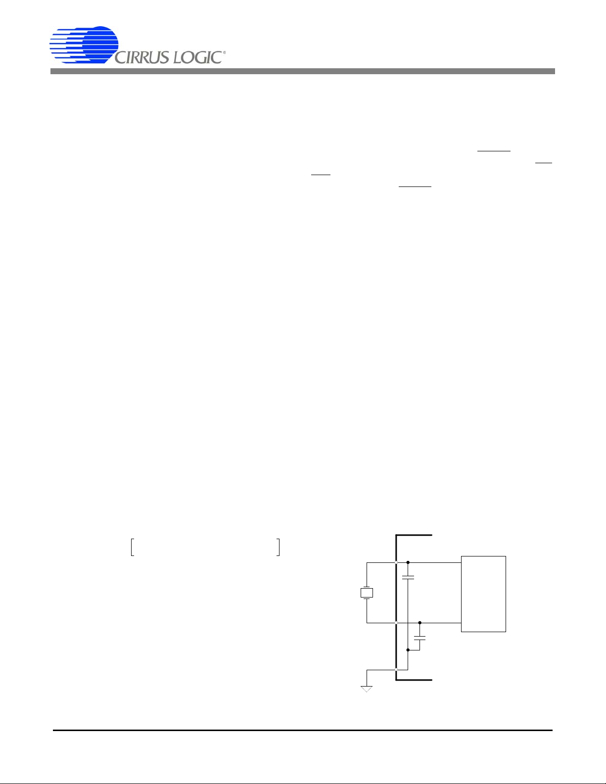
Oscillator
Circuit
DGND
XIN
XOUT
C1
C1 =
22 pF
C2
C2 =
Figure 10. Oscillator Connection
The temperature update rate is a function of the number
of ADC samples. With MCLK = 4.096 MHz and K = 1
the update rate is:
Cycle Count Register (N) must be set to a value
The
greater then one. Status bit TUP in the
Status Register,
indicates when the Temperature Register is updated.
The
Temperature Offset Register sets the zero-degree
measurement. To improve temperature measurement
accuracy, the zero-degree offset may need to be adjusted after the CS5463 is initialized. Temperature-offset
calibration is achieved by adjusting the
Offset Register
T) measured from a calibrated digital thermometer
(
(T
) by the differential temperature
off
Temperature
and the CS5463 temperature sensor. A one-degree adjustment to the
adding 2.737649x10
ter
(T
). Therefore,
off
if T
= -0.0951126 and T = -2.0 (°C), then
off
Temperature Register (T) is achieved by
-4
to the Temperature Offset Regis-
or 0xF3C168 (2’s compliment notation) is stored in the
Temperature Offset Register (T
To convert the
Temperature Register (T) from a Celsius
off
).
scale (°C) to a Fahrenheit scale (°F) utilize the formula
Applying the above relationship to the CS5461A temperature measurement algorithm
5.10 System Initialization
Upon powering up, the digital circuitry is held in reset
until the analog voltage reaches 4.0 V. At that time, an
eight-XIN-clock-period delay is enabled to allow the oscillator to stabilize. The CS5463 will then initialize.
A hardware reset is initiated when the RESET
pin is asserted with a minimum pulse width of 50 ns. The RESET signal is asynchronous, with a Schmitt-trigger
input. Once the RESET
eight-XIN-clock-period delay is enabled
pin is de-asserted, an
.
A software reset is initiated by writing the command
0x80. After a hardware or sof tware reset, the internal
registers (some of which drive output pins) will be reset
to their default values. Status bit DRDY in the
Register,
indicates the CS5463 is in its active state and
Status
ready to receive commands.
5.11 Power-down States
The CS5463 has two power-down states, Stand-by and
Sleep. In the stand-by state all circuitry except the volt-
age reference and crystal oscillator is turned off. To return the device to the active state, a power-up command
is sent to the device.
In Sleep state, all circuitry except the instruction decoder is turned off. When the power-up command is sent to
the device, a system initialization is performed (See
Section 5.10
System Initialization on page 20).
5.12 Oscillator Characteristics
XIN and XOUT are the input and output of an inverting
amplifier configured as an on-chip oscillator, as shown
in Figure 10. The oscillator circuit is designed to work
with a quartz crystal. To reduce circuit cost, two load capacitors C1 and C2 are integrated in the device, from
XIN to DGND, and XOUT to DGND. PCB trace lengths
should be minimized to reduce stray capacitance. To
If T
off
then the modified values are T
(0xF460E1) and T
Fahrenheit scale.
5.9 Voltage Reference
The CS5463 is specified for operation with a +2.5 V reference between the VREFIN and AGND pins. To utilize
the on-chip 2.5 V reference, connect the VREFOUT pin
to the VREFIN pin of the device. The VREFIN can be
used to connect external filtering and/or references.
20 DS678F3
= -0.09566 and T
= 23.507 for a Celsius scale,
gain
= 42.3132 (0x54A05E) for a
gain
off
= -0.09079
Page 21

CS5463
drive the device from an external clock source, XOUT
should be left unconnected while XIN is driven by the
external circuitry. There is an amplifier between XIN and
the digital section which provides CMOS level signals.
This amplifier works with sinusoidal inputs so there are
no problems with slow edge times.
The CS5463 can be driven by an external oscillator
ranging from 2.5 to 20 MHz, but the K divider value must
be set such that the internal MCLK will run somewhere
between 2.5 MHz and 5 MHz. The K divider value is set
with the K[3:0] bits in the
example, if XIN = MCLK = 15 MHz, and K is set to 5,
DCLK will equal 3 MHz, which is a valid value for DCLK.
Configuration Register. As an
5.13 Event Handler
The INT pin is used to indicate that an internal error or
event has taken place in the CS5463. Wr iting a logic 1
to any bit in the
bit in the
terrupt condition is cleared by writing a logic 1 to the bit
that has been set in the
The behavior of the INT
and IINV bits of the
IMODE IINV INT Pin
0 0 Active-low Level
0 1 Active-high Level
10 Low Pulse
11 High Pulse
If the interrupt output signal format is set for either falling
or rising edge, the duration of the INT
least one DCLK cycle (DCLK = MCLK/K).
Mask Register allows the corresponding
Status Register to activate the INT pin. The in-
Status Register.
pin is controlled by the IMODE
Configuration Register.
Table 4. Interrupt Configuration
pulse will be at
5.13.1 Typical Interrupt Handler
The steps below show how interrupts can be handled.
INITIALIZATION:
1) All Status bits are cleared by writing 0xFFFFFF to
the Status Register.
2) The condition bits which will be used to generate
interrupts are then set to logic 1 in the Mask Register.
3) Enable interrupts.
INTERRUPT HANDLER ROUTINE:
4) Read the Status Register.
5) Disable all interrupts.
6) Branch to the proper interrupt service routine.
7) Clear the Status Register by writing back the read
value in step 4.
8) Re-enable interrupt
9) Return from interrupt service routine.
This handshaking procedure ensures that any new interrupts activated between steps 4 and 7 are not lost
(cleared) by step 7.
5.14 Serial Port Overview
The CS5463 incorporates a serial port transmit and receive buffer with a command decoder that interprets
one-byte (8-bit) commands as they are received. Th ere
are four types of commands: instructions, synchronizing, register writes, and register reads (See Section
Commands on page 23).
5.16
Instructions are one byte in length and will interrupt any
instruction currently executing. Instructions do not affect
register reads currently being transmitted.
Synchronizing commands are one byte in length and
only affect the serial interface. Synchronizing commands do not affect operations currently in progress.
Register writes must be followed by three bytes of data.
Register reads can return up to four bytes of data.
Commands and data are transferred most-significant bit
(MSB) first. Figure 1 on page 12, defines the serial port
timing and required sequence necessary for writing to
and reading from the serial port receive and transmit
buffer, respectively. While reading data from the serial
port, commands and data can be written simultaneously. Starting a new register read command while data is
being read will terminate the current read in progress.
This is acceptable if the remainder of the current read
data is not needed. During data reads, the serial port requires input data. If a new command and data is not
sent, SYNC0 or SYNC1 must be sent.
5.14.1 Serial Port Interface
The serial port interface is a “4-wire” synchronous serial
communications interface. The inte rface is enabled to
start excepting SCLKs when CS
ed (logic 0). SCLK (Serial bit-clock) is a Schmitt-trigger
input that is used to strobe the data on SDI (Serial Data
In) into the receive buffer and out of the transmit buffer
onto SDO (Serial Data Out).
(Chip Select) is assert-
DS678F3 21
Page 22
CS5463
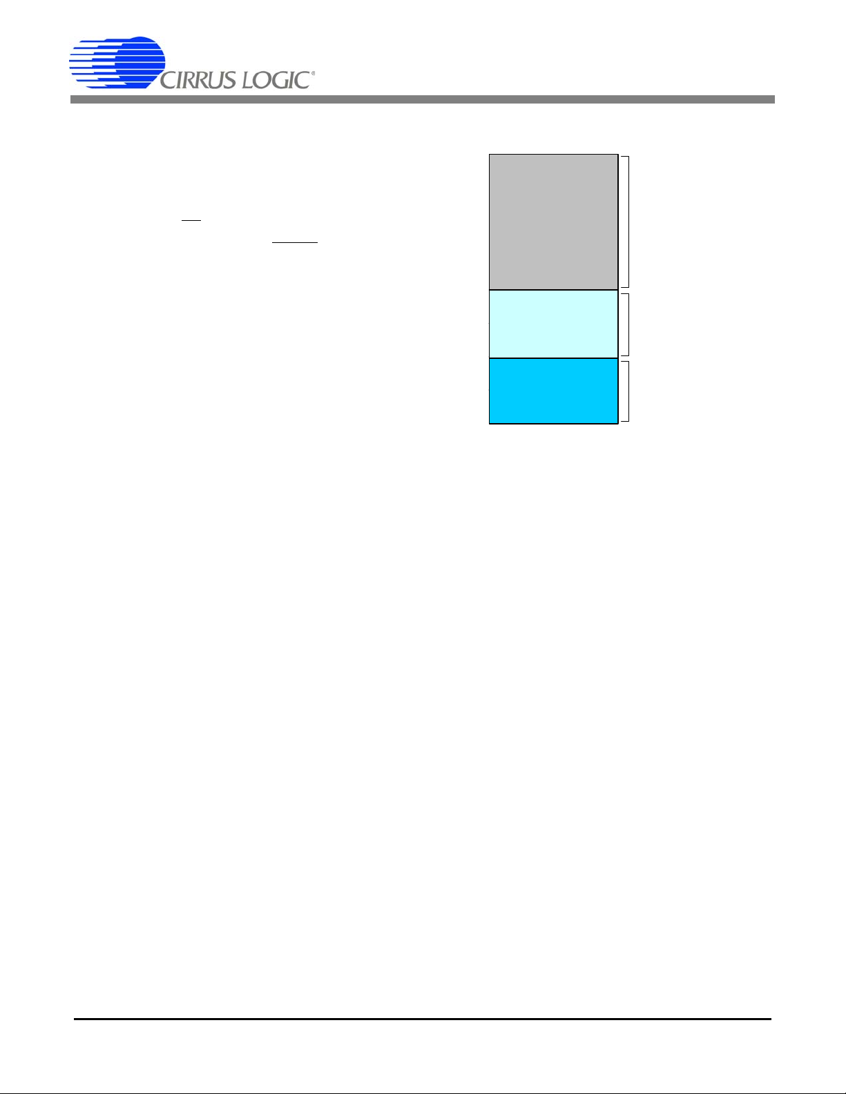
0xFFF
0x000
0x3FF
Hardware Registers*
32 Pages
Software Register*
32 Pages
ROM
2048 Words
0x400
0x7FF
0x800
Pages
0x40 - 0x7F
Pages
0x20 - 0x3F
Pages
0 - 0x1F
* Accessed using register read/write commands.
Figure 11. CS5463 Memory Map
If the serial port interface becomes unsynchronized with
respect to the SCLK input, any attempt to clock valid
commands into the serial interface may result in unexpected operation. Therefor, the serial port interface
must then be re-initialized by one of the following actions:
-Drive the CS
- Hardware Reset (drive RESET
pin high, then low.
pin low for at
least 10 µs).
- Issue the
Serial Port Initialization Sequence,
which is 3 (or more) SYNC1 command bytes
(0xFF) followed by one SYNC0 command byte
(0xFE).
If a re-synchronization is necessary, it is best to re-initialize the part either by hardware or software reset
(command 0x80), as the state of the part may be unknown.
5.15 Register Paging
Read/write commands access one of the 32 registers
within a specified page. By default, Page = 0. To access
registers in another page, the
Page Register (address
0x1F) must be written with the desired page number.
Example:
Reading register 6 in page 3.
1. Write 3 to page register with command and data:
0x7E 0x00 0x00 0x03
2. Read register 6 with command:
0x0C 0xFF 0xFF 0xFF
22 DS678F3
Page 23

CS5463
5.16 Commands
All commands are 8 bits in length. Any command byte value that is not listed in t his section is invalid. Commands
that write to registers must be followed by 3 bytes of data. Commands that read data can be chained with other commands (e.g., while reading data, a n ew command can be sent which can execu te durin g the o riginal rea d). All commands except register reads, register writes, and SYNC0 & SYNC1 will abort any currently executing commands.
5.16.1 Start Conversions
B7 B6 B5 B4 B3 B2 B1 B0
1110C3000
Initiates acquiring measurements and calculating results. The device has two modes of acquisition.
C3 Modes of acquisition/measurement
0 = Perform a single computation cycle
1 = Perform continuous computation cycles
5.16.2 SYNC0 and SYNC1
B7 B6 B5 B4 B3 B2 B1 B0
1111111SYNC
The serial port can be initialized by asserting CS or by sending three or more consecutive SYNC1 commands followed by a SYNC0 command. The SYNC0 or SYNC1 can also be sent while sending data out.
SYNC 0 = Last byte of a serial port re-initialization sequence.
1 = Used during reads and serial port initialization.
5.16.3 Power-up/Halt
B7 B6 B5 B4 B3 B2 B1 B0
10100000
If the device is powered-down, Power-Up/Halt will initiate a power on reset. If the part is already powered-on, all
computations will be halted.
5.16.4 Power-down and Software Reset
B7 B6 B5 B4 B3 B2 B1 B0
100S1S0000
To conserve power the CS5463 has two power-down states. In stand-by state all circuitry, e xcept the analog/digital
clock generators, is turned off. In the sleep state all circuitry, except the command decoder, is turned off. Bringing
the CS5463 out of sleep state requires more time than out of stand-by state, because of the extra time needed to
re-start and re-stabilize the analog oscillator.
S[1:0] Power-down state
00 = Software Reset
01 = Halt and enter stand-by power saving state. This stat e allo ws qu ick po wer-on
10 = Halt and enter sleep power saving state.
11 = Reserved
DS678F3 23
Page 24

CS5463
5.16.5 Register Read/Write
B7 B6 B5 B4 B3 B2 B1 B0
0W/R
The Read/Write informs the command decoder that a register access is required. During a read operation, the addressed register is loaded into an output buffer and clocked out by SCLK. During a
clocked into an input buffer and transferred to the addressed register upon completion of the 24
RA4 RA3 RA2 RA1 RA0 0
write operation, the data is
th
SCLK.
W/R
Write/Read control
0 = Read
1 = Write
RA[4:0] Register address bits (bits 5 through 1) of the read/write command.
Register Page 0
Address RA[4:0] Name Description
0 00000 Config Configuration
1 00001 I
2 00010 I
3 00011 V
4 00100 V
DCoff
gn
DCoff
gn
Current DC Offset
Current Gain
Voltage DC Offset
Voltage Gain
5 00101 Cycle Count Number of A/D conversions used in one computation cycle (N)).
6 00110 PulseRateE Sets the E1
, E2 and E3 energy-to-frequency output pulse rate.
7 00111 I Instantaneous Current
8 01000 V Instantaneous Voltage
9 01001 P Instantaneous Power
10 01010 P
11 01011 I
12 01100 V
13 01101
14 01110 P
Active
RMS
RMS
(Epsilon) Ratio of line frequency to output word rate (OWR)
off
Active (Real) Power
RMS Current
RMS Voltage
Power Offset
15 01111 Status Status
16 10000 I
17 10001 V
ACoff
ACoff
Current AC (RMS) Offset
Voltage AC (RMS) Offset
18 10010 Mode Operation Mode
19 10011 T Temperature
20 10100 Q
AVG
Average Reactive Power
21 10101 Q Instantaneous Reactive Power
22 10110 I
23 10111 V
24 11000 Q
Peak
Peak
Trig
Peak Current
Peak Voltage
Reactive Power calculated from Power Triangle
25 11001 PF Power Factor
26 11010 Mask Interrupt Mask
27 11011 S Apparent Power
28 11100 Ctrl Control
29 11101 P
30 11110 P
31 11111 Q
H
F
F
Harmonic Active Power
Fundamental Active Power
Fundamental Reactive Power / Page
Note: For proper operation,
do not attempt to write to unspecified registers.
24 DS678F3
Page 25

Register Page 1
Address RA[4:0] Name Description
0 00000 PulseWidth Energy Pulse Output Width
1 00001 Load
2 00010 T
3 00011 T
Gain
off
Min
No Load Threshold
Temperature Sensor Gain
Temperature Sensor Offset
Register Page 3
Address RA[4:0] Name Description
6 00110 VSAG
7 00111 VSAG
10 01010 ISAG
11 01011 ISAG
Duration
Level
Duration
Level
Voltage sag sample interval
Voltage sag level
Current fault sample interval
Current fault level
CS5463
Note: For proper operation,
do not attempt to write to unspecified registers.
5.16.6 Calibration
B7 B6 B5 B4 B3 B2 B1 B0
1 1 0 CAL4 CAL3 CAL2 CAL1 CAL0
The CS5463 can perform system calibrations. Proper input signals m ust be applied to the current and voltage channel before performing a designated calibration.
CAL[4:0]* Designates calibration to be performed
01001 = Current channel DC offset
01010 = Current channel DC gain
01101 = Current channel AC offset
01110 = Current channel AC gain
10001 = Voltage channel DC offset
10010 = Voltage channel DC gain
10101 = Voltage channel AC offset
10110 = Voltage channel AC gain
11001 = Current and Voltage channel DC offset
11010 = Current and Voltage channel DC gain
11101 = Current and Voltage channel AC offset
11110 = Current and Voltage channel AC gain
*For proper operation, values for CAL[4:0] not specified should not be used.
DS678F3 25
Page 26

CS5463
6. REGISTER DESCRIPTION
1. “Default” = bit status after power-on or reset
2. Any bit not labeled is Reserved. A zero should always be used when writing to one of these bits.
6.1 Page 0 Registers
6.1.1 Configuration Register ( Config )
Address: 0
23 22 21 20 19 18 17 16
PC6 PC5 PC4 PC3 PC2 PC1 PC0 Igain
15 14 13 12 11 10 9 8
EWA - - IMODE IINV - - -
76543210
- - -iCPUK3K2K1K0
Default = 0x000001
PC[6:0] Phase compensation. A 2’s complement number which sets a delay in the voltage channel rel-
ative to the current channel. Default setting is 000 0000 = 0.0215 degree phase delay at 60 Hz
(when MCLK = 4.096 MHz). See Section 7.2
mation.
Phase Compensation on page 39 for more infor-
I
gain
EWA Allows the E1
IMODE, IINV Interrupt configuration bits. Select the desired pin behavior for indication of an interrupt.
iCPU Inverts the CPUCLK clock. In order to reduce the level of noise present when analog signals
K[3:0] Clock divider. A 4-bit binary number used to divide the value of MCLK to generate the internal
Sets the gain of the current PGA.
0 = Gain is 10 (default)
1 = Gain is 50
and E2 pins to be configured as open-collector output pins.
0 = Normal outputs (default)
1 = Only the pull-down device of the E1
00 = Active-low level (default)
01 = Active-high level
10 = High-to-low pulse
11 = Low-to-high pulse
are sampled, the logic driven by CPUCLK should not be active durin g the sa mp le edge.
0 = Normal operation (default)
1 = Minimize noise when CPUCLK is driving rising edge logic
clock DCLK. The internal clock frequency is DCLK = MCLK/K. The value of K can range between 1 and 16. Note that a value of “0000” will set K to 16 (not zero). K = 1 at reset.
and E2 pins are active
26 DS678F3
Page 27

CS5463
6.1.2 Current and Voltage DC Offset Register ( I
DCoff
, V
DCoff
)
Address: 1 (Current DC Offset); 3 (Voltage DC Offset)
MSB LSB
-(20)2-12
-2
-3
2
-4
2
-5
2
-6
2
-7
2
.....
-17
2
-18
2
-19
2
-20
2
-21
2
-22
2
Default = 0x000000
The DC Offset registers (I
DCoff,VDCoff
) are initialized to 0.0 on reset. When DC Offset calibration is performed, the
register is updated with the DC offset measured over a computation cycle. DRDY will be set at the end of the
calibration. This register may be read and stored for future system offset compensation. The value is represented in two's complement notation and in the range of -1.0
the MSB. See Section 7.1.2.1
DC Offset Calibration Sequence on page 37 for more information.
6.1.3 Current and Voltage Gain Register ( I
gn
, V
gn )
I
DCoff,VDCoff
1.0, with the binary point to the right of
Address: 2 (Current Gain); 4 (Voltage Gain)
MSB LSB
1
2
0
2
-1
2
-2
2
-3
2
-4
2
-5
2
-6
2
.....
-16
2
-17
2
-18
2
-19
2
-20
2
-21
2
Default = 0x400000 = 1.000
The gain registers (I
gn,Vgn)
are initialized to 1.0 on reset. When either a AC or DC Gain calibration is performed,
the register is updated with the gain measured over a computation cycle. DRDY will be set at the end of the
calibration. This register may be read and stored for future system gain compe nsation. The value is in the range
0.0
I
< 3.9999, with the binary point to the right of the second MSB.
gn,Vgn
-23
2
-22
2
6.1.4 Cycle Count Register ( Cycle Count )
Address: 5
MSB LSB
23
2
22
2
21
2
20
2
19
2
18
2
17
2
16
2
.....
6
2
5
2
4
2
3
2
2
2
1
2
Default = 0x000FA0 = 4000
Cycle Count, denoted as N, determines the length of one
the computation cycle frequency is (MCLK/K)/(1024
computation cycle. During continuous conversions,
N). A one second computational cycle period occurs when
MCLK = 4.096 MHz, K = 1, and N = 4000.
6.1.5 PulseRateE Register ( PulseRateE )
Address: 6
MSB LSB
-(20)2-12
-2
Default = 0x800000 = 1.00 (2 kHz @ 4.096 MHz MCLK)
PulseRateE sets the frequency of E1, E2, & E3 pulses. E1, E2, E3 frequency = (MCLK x PulseRateE) / 2048 at
full scale. For a 4 khz sample rate, the maximum pulse rate is 2 khz. The va lue is re pr esente d in two's com plement notation and in the range is -1.0
values have the same effect as positive. See Section 5.5
-3
2
-4
2
-5
2
-6
2
-7
2
.....
-17
2
-18
2
-19
2
-20
2
-21
2
-22
2
PulseRateE 1.0, with the binary point to the right of the MSB. Negative
Energy Pulse Output on page 17 for more information.
0
2
-23
2
DS678F3 27
Page 28

CS5463
6.1.6 Instantaneous Current, Voltage, and Power Registers ( I , V , P )
Address: 7 (Instantaneous Current); 8 (Instantaneous Voltage); 9 (Instantaneous Power)
MSB LSB
-(20)2-12
-2
I and V contain the instantaneous measured values for current and voltage, respectively. The instantaneous
voltage and current samples are multiplied to obtain Instantaneous Power (P). The value is represented in two's
complement notation and in the range of -1.0
-3
2
-4
2
-5
2
-6
2
-7
2
.....
-17
2
-18
2
-19
2
-20
2
-21
2
-22
2
I, V, P 1.0, with the binary point to the right of the MSB.
-23
2
6.1.7 Active (Real) Power Register ( P
Active
)
Address: 10 (Active Power)
MSB LSB
0
-(2
)2-12
-2
-3
2
-4
2
-5
2
-6
2
-7
2
.....
-17
2
-18
2
-19
2
-20
2
-21
2
-22
2
The instantaneous power is averaged over each computation cycle (N conversions) to compute Active Power
). The value will be within in the range of -1.0 P
(P
Active
1.0. The value is represented in two's complement
Active
notation, with the binary point to the right of the MSB.
6.1.8 RMS Current & Voltage Registers ( I
Address: 11 (I
MSB LSB
-1
2
I
RMS
-2
2
and V
RMS
value is represented in unsigned binary notation and in the range of 0.0
2
RMS
-3
); 12 (V
-4
2
RMS
2
)
-5
-6
2
-7
2
contain the Root Mean Square (RMS) values of I and V, calculated each computation cycle. The
RMS
2
, V
-8
RMS
.....
)
-18
2
-19
2
I
RMS,VRMS
-20
2
-21
2
-22
2
-23
2
1.0, with the binary point
to the left of the MSB.
6.1.9 Epsilon Register ( )
Address: 13
MSB LSB
0
)2-12
-(2
-2
-3
2
-4
2
-5
2
-6
2
-7
2
.....
-17
2
-18
2
-19
2
-20
2
-21
2
-22
2
-23
2
-24
2
-23
2
Default = 0x01999A = 0.0125 sec
Epsilon (
ing Measurements
value is represented in two's complement notation and in the range of -1.0
) is the ratio of the input line frequency to the sample frequency of the ADC (See Section 5.4 Perform-
on page 16). Epsilon is either written to the register, or measured during conversions. The
1.0, with the binary point to the
right of the MSB. Negative values have no significance.
28 DS678F3
Page 29

CS5463
6.1.10 Power Offset Register ( P
off
)
Address: 14
MSB LSB
-(20)2-12
-2
-3
2
-4
2
-5
2
-6
2
-7
2
.....
-17
2
-18
2
-19
2
-20
2
-21
2
-22
2
Default = 0x000000
Power Offset (P
) is added to the instantaneous power being accumulated in the P
off
register, and can be
active
used to offset contributions to the energy result that are caused by undesirab le sources of energy that are inherent in the system. The value is represented in two's complement notation and in the range of -1.0
Poff 1.0,
with the binary point to the right of the MSB.
6.1.11 Status Register and Mask Register ( Status , Mask )
Address: 15 (Status Register); 26 (Mask Register)
23 22 21 20 19 18 17 16
DRDY CRDY IOR VOR
15 14 13 12 11 10 9 8
IROR VROR EOR IFAULT VSAG
76543210
TUP TOD VOD IOD LSD FUP
Default = 0x800001 (Status Register), 0x000000 (Mask Register)
IC
-23
2
The Status Register indicates status within the chip. In normal operation, writing a '1' to a bit will cause the bit
to reset. Writing a '0' to a bit will not change it’s current state.
The Mask Register is used to control the activation of the INT
corresponding bit in the Status Register to activate the INT
pin. Placing a logic '1' in a Mask bit will allow the
pin when the status bit is asserted.
DRDY Data Ready. During conversions, this bit will indicate the end of computation cycles. For cali-
brations, this bit indicates the end of a calibration sequence.
CRDY Conversion Ready. Indicates a new conversion is ready. This will occur at the output word rate.
IOR Current Out of Range. Set when the
VOR Voltage Out of Range. Set when the
IROR I
VROR V
Out of Range. Set when the I
RMS
Out of Range. Set when the V
RMS
EOR Energy Out of Range. Set when P
IFAULT Indicates a current fault has occurred. See Section 5.6
Instantaneous Current Register overflows.
Instantaneous Voltage Register overflows.
Register overflows.
RMS
Register overflows.
RMS
ACTIVE
overflows.
Sag and Fault Detect Feature on page
19.
VSAG Indicates a voltage sag has occurred. See Section 5.6
Sag and Fault Detect Feature on page
19.
TUP Temperature Updated. Indicates the
Temperature Register has updated.
TOD Modulator oscillation detected on the temperature channel. Set when the modulator oscillates
due to an input above full scale.
VOD (IOD) Modulator oscillation detected on the voltage (current) channel. Set when the modulator oscil-
DS678F3 29
Page 30

CS5463
lates due to an input above full scale. The level at which the modulator oscillates is significantly
higher than the voltage channel’s differential input voltage (current) range.
Note:
The IOD and VOD bits may be ‘falsely’ triggered by very brief voltage spikes from the
power line. This event should not be confused with a DC overload situation at the inputs,
when the IOD and VOD bits will re-assert themselves even after being cleared, multiple
times.
LSD Low Supply Detect. Set when the voltage at the PFMON pin fa lls below the low-voltage thresh-
old (PMLO), with respect to AGND pin. The LSD bit cannot be reset until the voltage at PFMON
pin rises back above the high-voltage threshold (PMHI).
FUP Epsilon Updated. Indicates completion of a line frequency measurement and update of Epsilon.
IC
6.1.12 Current and Voltage AC Offset Register ( V
Invalid Command. Normally logic 1. Set to logic 0 if an invalid command is received or the Sta-
tus Register
has not been successfully read.
ACoff
, I
ACoff
)
Address: 16 (Current AC Offset); 17 (Voltage AC Offset)
MSB LSB
-(20)2-12
-2
-3
2
-4
2
-5
2
-6
2
-7
2
.....
-17
2
-18
2
-19
2
-20
2
-21
2
-22
2
Default = 0x000000
The AC Offset Registers (V
ACoff, IACoff) are initialized to zero on reset, allowing for uncalibrated normal operation .
AC Offset Calibration updates these registers. This sequence lasts approximately (6N + 30) ADC cycles (where
N is the value of the
Cycle Count Register). DRDY will be asserted at the end of the calibration. These values
may be read and stored for future system AC offset compensation. The value is represented in two's complement notation in the range of -1.0
VACoff, IACoff 1.0, with the binary point to the right of the MSB
6.1.13 Operational Mode Register ( Mode )
Address: 18
23 22 21 20 19 18 17 16
15 14 13 12 11 10 9 8
E2MODE XVDEL
-23
2
76543210
XIDEL IHPF VHPF IIR
E3MODE1 E3MODE0 POS AFC
Default = 0x000000
E2MODE E2
Output Mode
0 = Energy Sign (default)
1 = Apparent Power
XVDEL Enables an extra sample of voltage channel delay. XVDEL and XIDEL can not be enabled at
the same time.
XIDEL Enables an extra sample of current channel delay. XVDEL and XIDEL can not be enabled at
the same time.
30 DS678F3
Page 31

IHPF (VHPF) Enables the high-pass filter on the current (voltage) channel.
0 = High-pass filter disabled (default)
1 = High-pass filter enabled
When either IHPF or VHPF are enabled, but not both, an all-pass filter is applied to the
Note:
opposite channel for phase matching.
IIR Enables the IIR compensation filters.
0 = IIR compensation filters enabled (default)
1 = IIR compensation filters disabled
CS5463
E3MODE[1:0] E3
Output Mode
00 = Reactive Power (default)
01 = PFMON
10 = Voltage sign
11 = Apparent Power
POS Positive Energy Only. Negative energy pulses on E1
press negative
P Register results.
are suppressed. However, it will NOT sup-
AFC Enables automatic line-frequency measurement and set s the frequency of the local sine/cosine
generator used in fundamental/harmonic measurements. When AFC is enabled, the Epsilon
register will be updated periodically.
6.1.14 Temperature Register ( T )
Address: 19
MSB LSB
-(27)262
5
T contains measurements from the on-chip temperature sensor. Measurements are performed during continuous conversions, with the default the Celsius scale (
and in the range of -128.0
6.1.15 Average and Instantaneous Reactive Power Register ( Q
Address: 20 (Average Reactive Power) and 21 (Instantaneous Reactive Power)
4
2
3
2
2
2
1
2
0
.....
2
o
C). The value is represented in two's complement notation
-10
2
-11
2
-12
2
-13
2
-14
2
-15
2
T 128.0, with the binary point to the right of the eighth MSB.
, Q )
AVG
-16
2
MSB LSB
-(20)2-12
-2
-3
2
-4
2
-5
2
-6
2
-7
2
.....
-17
2
-18
2
-19
2
-20
2
-21
2
-22
2
-23
2
The Instantaneous Reactive Power (Q) is the product of the voltage, shifted 90 degrees, and the current. The
Average Reactive Power (Q
is represented in two's complement notation and in the range of -1.0
) is Q averaged over N samples. The results are signed values with. The value
AVG
Q, Q
1.0, with the binary point to the
AVG
right of the MSB.
6.1.16 Peak Current and Peak Voltage Register ( I
peak , Vpeak
)
Address: 22 (Peak Currect) and 23 (Peak Voltage)
MSB LSB
0
-(2
)2-12
The Peak Current (I
-2
-3
2
peak
-4
2
-5
2
) and Peak Voltage (V
-6
2
-7
2
peak
.....
) registers contain the instantaneous current and voltage with
-17
2
-18
2
-19
2
-20
2
-21
2
-22
2
-23
2
the greatest magnitude detected during the last computation cycle. The value is represented in two's comple-
ment notation and in the range of -1.0
I
peak,Vpeak
1.0, with the binary point to the right of the MSB.
DS678F3 31
Page 32

CS5463
6.1.17 Reactive Power Register ( Q
Trig
)
Address: 24
MSB LSB
0
-1
2
The Reactive Power (Q
on page 14). The value is represented in u nsigned notation and in the rang e of 0
-2
2
-3
2
-4
2
) is calculated using trigonometric identities. (See Section 4.3 Power Measurem ents
Trig
-5
2
-6
2
-7
2
.....
-17
2
-18
2
-19
2
-20
2
-21
2
-22
2
S 1.0, with the binary point
to the right of the MSB.
6.1.18 Power Factor Register ( PF )
Address: 25
MSB LSB
0
-(2
)2-12
-2
-3
2
-4
2
-5
2
-6
2
-7
2
.....
-17
2
-18
2
-19
2
-20
2
-21
2
-22
2
Power Factor is calculated by dividing the Active (Real) Power by Apparent Power. The value is represented in
two's complement notation and in the range of -1.0
PF 1.0, with the binary point to the right of the MSB.
6.1.19 Apparent Power Register ( S )
Address: 27
MSB LSB
0
-1
2
-2
2
-3
2
-4
2
-5
2
-6
2
-7
2
.....
-17
2
-18
2
-19
2
-20
2
-21
2
-22
2
-23
2
-23
2
-23
2
Apparent power (S) is the product of the V
the range of 0
S 1.0, with the binary point to the right of the MSB.
RMS
and I
, The value is represented in unsigned notatio n and in
RMS
32 DS678F3
Page 33
CS5463
6.1.20 Control Register ( Ctrl )
Register Address: 28
23 22 21 20 19 18 17 16
15 14 13 12 11 10 9 8
STOP
76543210
INTOD NOCPU NOOSC
Default = 0x000000
STOP Terminates the auto-boot sequence.
0 = Normal (default)
1 = Stop sequence
INTOD Converts INT
output pin to an open drain output.
0 = Normal (default)
1 = Open drain
NOCPU Saves power by disabling the CPUCLK pin.
0 = Normal (default)
1 = Disables CPUCLK
NOOSC Saves power by disabling the crystal oscillator.
0 = Normal (default)
1 = Disabling oscillator circuit
6.1.21 Harmonic Active Power Register ( PH )
Address: 29
MSB LSB
0
-(2
)2-12
The Harmonic Active Power (P
(Real) Power. The value is represented in two's complement notation and in the range of -1.0
-2
-3
2
-4
2
-5
2
) is calculated by subtracting the Fundamental Active Power from the Active
H
-6
2
-7
2
.....
-17
2
-18
2
-19
2
-20
2
-21
2
-22
2
PH 1.0, with
the binary point to the right of the MSB.
6.1.22 Fundamental Active Power Register ( PF )
Address: 30
-23
2
MSB LSB
0
-(2
)2-12
The Fundamental Active Power (P
-2
-3
2
-4
2
-5
2
F
-6
2
-7
2
.....
-17
2
-18
2
-19
2
-20
2
-21
2
-22
2
2
) is calculated by performing a discrete Fourier transform (DFT) at the rele-
-23
vant frequency on the V and I channels. The results are multiplied to yield fundamental power. The value is represented in two's complement notation and in the range of -1.0
PH 1.0, with the binary point to the right of
the MSB.
DS678F3 33
Page 34

CS5463
6.1.23 Fundamental Reactive Power Register ( QH )
Address: 31 (read only)
MSB LSB
-(20)2-12
-2
Fundamental Reactive Power (QH) is calculated by performing a discrete Fourier transform (DFT) at the relevant
frequency on the V and I channels. The value is represented in two's complem ent no tation a nd in the ra ng e of
QH 1.0, with the binary point to the right of the MSB.
-1.0
6.1.24 Page Register
Address: 31 (write only)
MSB LSB
6
2
5
2
4
2
Default = 0x00
Determines which register page the serial port will access.
-3
2
3
2
-4
2
2
2
-5
2
2
-6
2
1
0
2
-7
2
.....
-17
2
-18
2
-19
2
-20
2
-21
2
-22
2
-23
2
34 DS678F3
Page 35

CS5463
6.2 Page 1 Registers
6.2.1 Energy Pulse Output Width ( PulseWidth )
Address: 0
MSB LSB
02
22
Default = 1
21
2
20
2
19
2
18
2
17
2
16
2
.....
6
2
5
2
4
2
3
2
2
2
1
2
0
2
PulseWidth sets the duration of energy pulses (t
). The actual pulse duration is the contents of PulseW idth
PW
divided by the output word rate (OWR). PulseWidth is an integer in the range of 1 to 8388607.
6.2.2 No Load Threshold ( Load
Min
)
Address: 1
MSB LSB
-(20)2-12
-2
-3
2
-4
2
-5
2
-6
2
-7
2
.....
-17
2
-18
2
-19
2
-20
2
-21
2
-22
2
Default = 0
Load
the active energy pulse output will be disabled. Load
-1.0
6.2.3 Temperature Gain Register ( T
is used to set the no load threshold. When the magnitude of the P
Min
Load
1.0, with the binary point to the right of the MSB. Negative values are not used.
Min
)
Gain
is a two's complement value in the range of
Min
register is less than Load
Active
Address: 2
MSB LSB
6
2
5
2
4
2
3
2
2
2
1
2
0
2
-1
2
.....
-11
2
-12
2
-13
2
-14
2
-15
2
-16
2
Default = 0x2F03C3 = 23.5073471
Sets the temperature channel gain. Temperature gain (T
o
to another. The Celsius scale (
C) is the default. Values will be within in the range of 0 T
is represented in unsigned notation, with the binary point to the right of bit 7th MSB. See Section 5.8
Temperature Sensor
on page 19.
) is utilized to convert from one temperature scale
Gain
128. The value
Gain
On-chip
-23
2
Min
-17
2
,
6.2.4 Temperature Offset Register ( T
Off
)
Address: 3
MSB LSB
0
-(2
)2-12
-2
-3
2
-4
2
-5
2
-6
2
-7
2
.....
-17
2
-18
2
-19
2
-20
2
-21
2
-22
2
-23
2
Default = 0xF3D35A = -0.0951126
Temperature offset (T
are represented in two's complement notation and in the range of -1.0
) is used to remove the temperature channel’s offset at the zero- degree reading. Values
off
T
1.0, with the binary point to the
off
right of the MSB.
DS678F3 35
Page 36

6.3 Page 3 Registers
CS5463
6.3.1 Voltage Sag and Current Fault Duration Registers ( VSAG
Duration
, ISAG
Duration
)
Address: 6 (Voltage Sag Duration); 10 (Current Fault Duration)
MSB LSB
0
22
2
21
2
20
2
19
2
18
2
17
2
16
2
.....
6
2
5
2
4
2
3
2
2
2
1
2
Default = 0x000000
Voltage Sag Duration (VSAG
) and Current Fault Duration (ISAG
Duration
) defines the number of instanta-
Duration
neous measurements utilized to determine a sag event. Setting these register to zero will disable this feature.
The value is represented in unsigned notation. See Section 5.6
6.3.2 Voltage Sag and Current Fault Level Registers ( VSAG
Sag and Fault Detect Feature on page 19.
Level
, ISAG
Level
)
Address: 7 (Voltage Sag Level ); 11 (Current Fault Level )
MSB LSB
02-12
-2
-3
2
-4
2
-5
2
-6
2
-7
2
.....
-17
2
-18
2
-19
2
-20
2
-21
2
-22
2
Default = 0x000000
Voltage Sag Level (VSAG
) and Current Fault Level (ISAG
Level
) defines the voltage level that the magnitude
Level
of input samples, averaged over the sag duration, must fall below in order to register a sag/fault condition. These
value are represented in unsigned notation and in the range of 0
right of the third MSB. See Section 5.6
Sag and Fault Detect Feature on page 19.
VSAG
1.0, with the binary point to the
Level
0
2
-23
2
36 DS678F3
Page 37
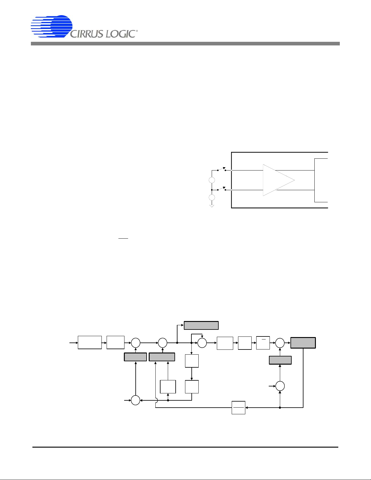
7. SYSTEM CALIBRATION
Figure 12. Calibration Data Flow
In
Modulator
+
X
to V*, I* Registers
Filter
N
V
RMS
*, I
RMS
*
Registers
DC Offset*
Gain*
0.6
+
+
+
* Denotes readable/writable register
N
+
X
N
Inver se
X
-1
RMS
AC O ffs e t*
N
X
-1
+
+
-
XGAIN
+
-
External
Connections
0V
+
-
AIN+
AIN-
CM
+
-
Figure 13. System Calibration of Offset
CS5463
7.1 Channel Offset and Gain Calibration
The CS5463 provides digital DC offset and gain compensation that can be applied to the instantaneous voltage and current measurements, and AC offset
compensation to the voltage an d current RMS calculations.
Since the voltage and current channels have independent offset and gain registers, system offset and/or
gain can be performed on either channel without the
calibration results from one channel affecting the other.
The computational flow of the calibration sequences are
illustrated in Figure 12. The flow applies to both the voltage channel and current channel.
7.1.1 Calibration Sequence
The CS5463 must be operating in its active state and
ready to accept valid commands. Refer to Section 5.16
Commands on page 23. The calibration algorithms are
dependent on the value N in the
(see Figure 12). Upon completion, the results of the calibration are available in their corresponding register.
The DRDY bit in the
Status Register will be set. If the
DRDY bit is to be output on the INT
in the Mask Register must be set. The initial values in
the AC gain and offset registers do affect the results of
the calibration results.
7.1.1.1 Duration of Calibration Sequence
The value of the Cycle Count Register (N) determines
the number of conversions performed by the CS5463
during a given calibration sequence. For DC offset and
gain calibrations, the calibration sequence takes at least
Cycle Count Register
pin, then DRDY bit
N + 30 conversion cycles to complete. For AC offset calibrations, the sequence takes at least 6N + 30 ADC cycles to complete, (about 6 computation cycles). As N is
increased, the accuracy of calibration results will increase.
7.1.2 Offset Calibration Sequence
For DC and AC offset calibrations, the VIN pins of the
voltage and IIN
connected to their ground referenc e level. (see Figure
13.)
The AC offset registers must be set to the default
(0x000000).
7.1.2.1 DC Offset Calibration Sequence
Channel gain should be set to 1.0 when performing DC
offset calibration. Initiate a DC offset calibration. The DC
offset registers are updated with the negative of the average of the instantaneous samples collected over a
computational cycle. Upon completion of the DC offset
calibration the DC offset is stored in the correspo nding
DC offset register. The DC offset value will be added to
pins of the current channels should be
DS678F3 37
Page 38
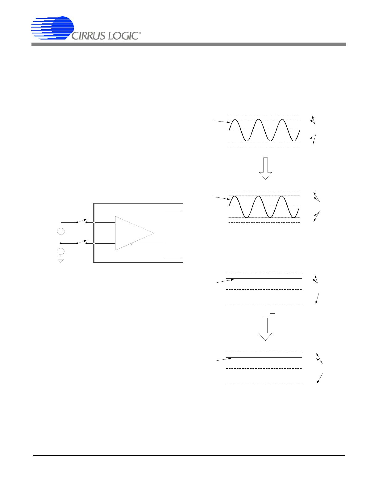
CS5463
+
-
+
-
External
Connections
IN+
IN-
CM
+
-
+
-
XGAIN
Reference
Signal
Figure 14. System Calibration of Gain.
V
RMS
Register =
230
/
x
1
/
250
0.65054
250 mV
230 mV
0 V
-230 mV
-250 mV
0.9999...
0.92
-0.92
-1.0000...
V
RMS
Register =0.600000
250 mV
230 mV
0 V
-230 mV
-250 mV
0.84853
-0.84853
Before AC Gain Calibration (Vgn Register = 1)
After AC Gain Calibration (Vgn Register changed to approx. 0.9223)
Instantaneous Voltage
Register Values
Instantaneous Voltage
Register Values
Sinewave
Sinewave
0.92231
-0.92231
INPUT
SIGNAL
INPUT
SIGNAL
Figure 15. Example of AC Gain Calibration
V
RMS
Register =
230
=0.92
250 mV
230 mV
0 V
-250 mV
0.9999...
0.92
-1.0000...
V
RMS
Register =0.600000
250 mV
230 mV
0 V
-250 mV
0.6000
Before AC Gain Calibration (Vgain Register = 1)
After AC Gain Calibration (Vgain Register changed to approx. 0.65217)
Instantaneous Voltage
Register Values
Instantaneous Voltage
Register Values
DC Signal
DC Signal
0.65217
-0.65217
INPUT
SIGNAL
INPUT
SIGNAL
250
Figure 16. Example of AC Gain Calibration
each instantaneous measurement to nullify the DC
component present in the system during conversion
commands.
7.1.2.2 AC Offset Calibration Sequence
Corresponding offset registers I
should be cleared prior to initiating AC offset calibrations. Initiate an AC offset calibration.The AC offset registers are updated with an offset value that reflects the
RMS output level. Upon completion of the AC offset calibration the AC offset is stored in the corresponding AC
offset register. The AC offset register value is subtracted from each successive V
RMS
and I
and/or V
ACoff
RMS
ACoff
calculation.
7.1.3 Gain Calibration Sequence
When performing gain calibrations, a reference signal
should be applied to the VIN
pins of the current channels that represents the de -
IIN
sired maximum signal level. Figure 14 shows the basic
setup for gain calibration.
pins of the voltage and
A typical rms calibration value which allows for reasonable over-range margin would be 0.6 or 60% of the voltage and current channel’s maximum input voltage level.
Two examples of AC gain calibration and the updated
digital output codes of the channel’s instantaneous data
registers are shown in Figures 15 and 16. Figure 16
For gain calibrations, there is an absolute limit on the
RMS voltage levels that are selected for the gain calibration input signals. The maximum value that the gain
registers can attain is 4. Therefore, if the signal level of
the applied input is low enough that it causes the
CS5463 to attempt to set either gain register highe r than
4, the gain calibration result will be invalid and all
CS5463 results obtained while performing measurements will be invalid.
If the channel gain registers are initially set to a gain other then 1.0, AC gain calibration should be used.
7.1.3.1 AC Gain Calibration Sequence
The corresponding gain regist er should be set to 1.0,
unless a different initial gain value is desired. Initiate an
AC gain calibration. The AC gain calibration algorithm
computes the RMS value of the reference signal applied
to the channel inputs. The RMS register value is then divided into 0.6 and the quotient is stored in the corresponding gain register. Each instantaneous
measurement will be multiplied by its corresponding AC
gain value.
38 DS678F3
shows that a positive (or negative) DC-level signal can
be used even though an AC gain calibration is being executed.
Page 39

CS5463
Freq = Line Frequency [Hz]
XDEL = XVDEL or -XIDEL
Phase
Freq 360
o
PC 5:0 PC 6 64– XDEL 128+
MCLK K8
---------------------------------------------------------------------------------------------------------------------------------
=
However, an AC signal cannot be used for DC gain calibration.
7.1.3.2 DC Gain Calibration Sequence
Initiate a DC gain calibration. The corresponding gain
register is restored to default (1.0). The DC gain calibration averages the channel’s instantaneous measurements over one computation cycle (N samples). The
average is then divided into 1.0 and the quotient is
stored in the corresponding gain register
After the DC gain calibration, the instantaneous register
will read at full-scale whenever the DC level of the input
signal is equal to the level of the DC calibration signal
applied to the inputs during the DC gain calibration.The
HPF option should not be enabled if DC gain calibration
is utilized.
7.1.4 Order of Calibration Sequences
1. If the HPF option is enabled, then any DC component
that may be present in the selected signal path will be
removed and a DC offset calibration is not require d.
However, if the HPF option is disabled the DC offset
calibration sequence should be performed.
When using high-pass filters, it is recommended that
the DC Offset register for the corresponding channel
be set to zero. When performing DC offset calibration, the corresponding gain channel should be set to
one.
2. If there is an AC offset in the V
RMS
or I
tion, then the AC offset calibration sequence should
be performed.
3. Perform the gain calibration sequence.
4. Finally, if an AC offset calibration was performed
(step 2), then the AC offset may need to be adjusted
to compensate for the change in gain (step 3). This
can be accomplished by restoring zero to the AC offset register and then perform an AC offset calibration
sequence. The adjustment could also be done by
multiplying the AC offset register value that was cal-
RMS
calcula-
culated in step 2 by the gain calculated in step 3 and
updating the AC offset register with the product.
7.2 Phase Compensation
The CS5463 is equipped with phase compensation to
cancel out phase shifts introduced by the measurement
element. Phase Compensation is set by bits PC[6:0] in
Configuration Register and bits XVDEL and XIDEL
the
Operational Mode Register
in the
The default value of PC[6:0], XVDEL, and XIDEL is ze-
ro. With MCLK = 4.096 MHz and K = 1, the phase compensation has a range of
8.1 degrees when the input
signals are 60 Hz. Under these conditions, each step of
the phase compensation register (value of one LSB) is
approximately 0.04 degrees. For values of MCLK other
than 4.096 MHz, the range and step size should be
scaled by 4.096 MHz/(MCLK/K). For power line frequencies other than 60Hz, the values of the range and
step size of the PC[6:0] bits can be determined by converting the above values from angular measurement
into the time domain (seconds), and then computing the
new range and step size (in degrees) with resp ect to the
new line frequency. To calculate the phase shift induced
between the voltage and the current channel use the
equation:
7.3 Active Power Offset
The Power Offset Register can be used to offset system
power sources that may be resident in the system, but
do not originate from the power line signal. These sources of extra energy in the system contribute undesirable
and false offsets to the power and energy measurement
results. After determining the amount of stray power, the
Power Offset Register can be set to cancel the effects
of this unwanted energy.
DS678F3 39
Page 40
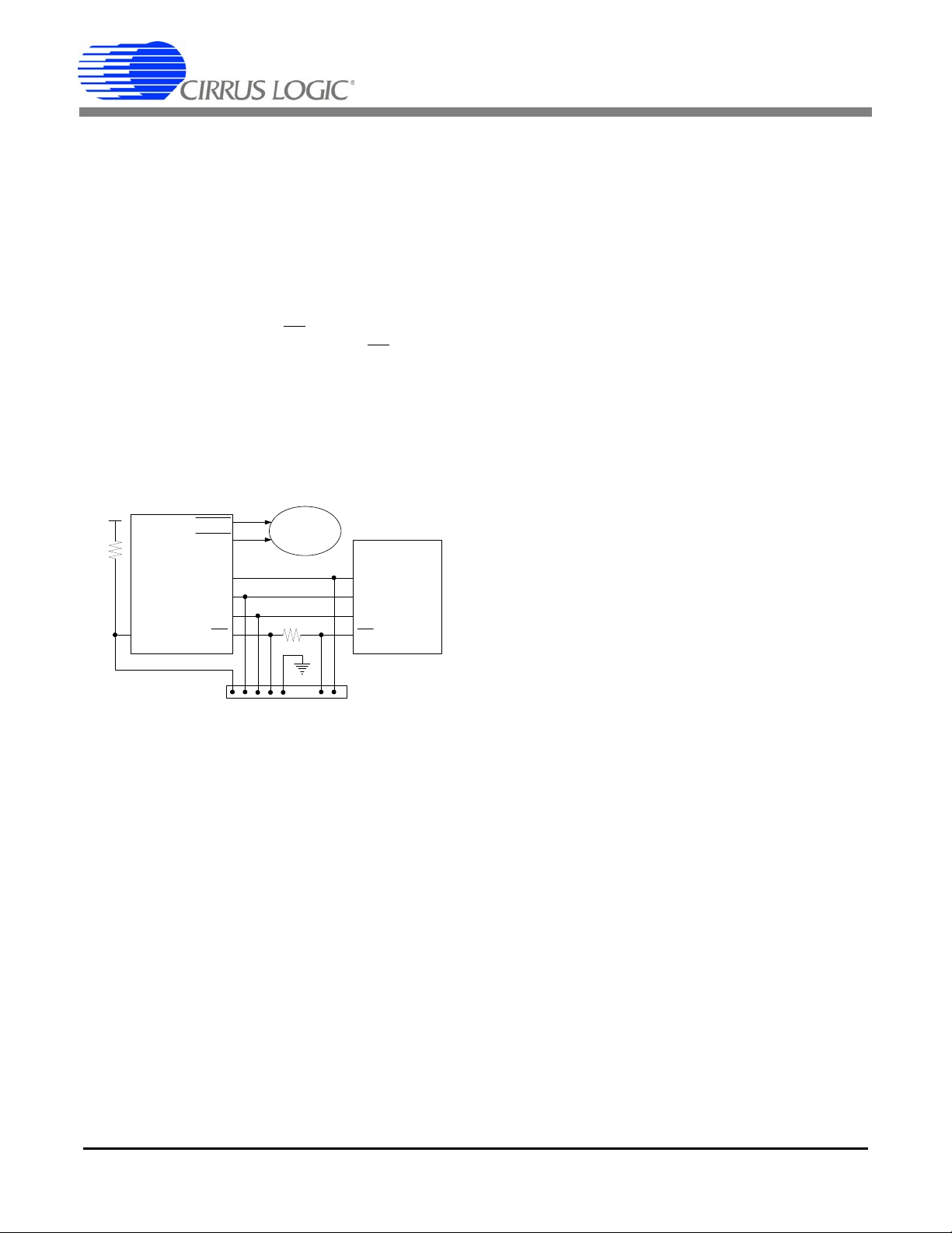
8. AUTO-BOOT MODE USING E2PROM
CS5463
EEPROM
EOUT1
EOUT2
MODE
SCLK
SDI
SDO
CS
SCK
SO
SI
CS
Connector to Calibrator
VD+
5 K
5 K
Mech. Counter
Stepper Motor
or
Figure 17. Typical Interface of E2PROM to CS5463
When the CS5463 MODE pin is asserted (logic 1), the
CS5463
the CS5463 downloads the required commands and
register data from an external serial E
the CS5463 to begin performing energy measur ements.
8.1 Auto-boot Configuration
A typical auto-boot serial connection between the
CS5463 and a E
to-boot mode, the CS5463’s CS
ured as outputs. The CS5463 asserts CS
provides a clock on SCLK, and sends a read command
to the E
er-specified commands and register data presented on
the SDI pin. The E
by the CS5463 to change the designated registers’ default values and begin registering energy.
auto-boot mode is enabled. In auto-boot mode,
2
PROM, allowing
2
PROM is illustrated in Figure 17. In au-
and SCLK are config-
(logic 0),
2
PROM on SDO. The CS5463 reads the us-
2
PROM’s programmed data is utilized
CS5463
commands/data will determine the CS5463’s exact operation, when the auto-boot initialization sequence is
running. Any of the valid commands can be used.
8.2 Auto-boot Data for E2PROM
Below is an example code set for an auto-boot sequence. This code is written into the E
er. The serial data for such a sequence is shown below
in single-byte hexidecimal notation:
-64 00 00 60
Write Operation Mode Register, turn high-pass
filters on.
-44 7F C4 A9
Write value of 0x7FC4A9 to Current Gain
Register.
-48 FF B2 53
Write value of 0xFFB253 to Voltage Gain
Register.
-74 00 00 04
Unmask bit #2 (LSD) in the Mask Register.
-E8
Start continuous conversions
-78 00 01 00
Write STOP bit to Control Register, to terminate
auto-boot initialization sequence.
2
PROM by the us-
8.3 Which E2PROMs Can Be Used?
Several industry-standard serial E2PROMs that will successfully run auto-boot with the CS5461A are listed below:
• Atmel AT25010, AT25020 or AT25040
• National Semiconductor NM25C040M8 or NM25020M8
Figure 17 also shows the external connections that
would be made to a calibrator device, such as a PC or
custom calibration board. When the metering system is
installed, the calibrator would be used to control calibration and/or to program user-specified commands and
calibration values into the E
2
PROM. The user-specified
40 DS678F3
• Xicor X25040SI
These types of serial E2PROMs expect a specific 8-bit
command (00000011) in order to perform a memory
read. The CS5461A has been hardware progra mmed to
transmit this 8-bit command to the E
2
PROM at the be-
ginning of the auto-boot sequence.
Page 41

9. BASIC APPLICATION CIRCUITS
VA+ VD+
CS5463
0.1 µF470 µF
500
470 nF
500
N
R
1
R
2
10
14
VIN+
9
VIN-
IIN-
10
15
16
IIN+
PFMON
CPUCLK
XOUT
XIN
Optional
Clock
Source
Serial
Data
Interface
RESET
17
2
1
24
19
CS
7
SDI
23
SDO
6
SCLK
5
INT
20
E1
0.1 µF
VREFIN
12
VREFOUT
11
AGND DGND
13 4
3
4.096 MHz
0.1 µF
10 k
5k
L
R
Shunt
R
V-
R
I-
R
I+
ISOLATION
120 VAC
Mech. Counter
Stepper Motor
or
22
21
C
I-
C
I+
C
Idiff
C
V-
C
V+
C
Vdiff
E2
Note:
Indicates common (floating) return.
Figure 18. Typical Connection Diagram (Single-phase, 2-wire – Direct Connect to Power Line)
Figure 18 shows the CS5463 configured to measure
power in a single-phase, 2-wire syste m while op erat ing
in a single-supply configuration. In this diagram, a shunt
resistor is used to sense the line current and a voltage
divider is used to sense the line voltage. In this type of
shunt-resistor configuration, the common-mode le vel of
the CS5463 must be referenced to the line side of the
power line. This means that the common -mode potential of the CS5463 will track the high-voltage levels, as
well as low-voltage levels, with respect to earth ground.
Isolation circuitry is required when an earth-ground-referenced communication interface is connected.
CS5463
Figure 19 shows the same single-phase, two-wire sys-
tem with complete isolation from the power lines. This
isolation is achieved using three transformers: a general
purpose transformer to supply the on-board DC power;
a high-precision, low-impedance voltage transformer,
with very little roll-off/phase-delay, to measure voltage;
and a current transformer to sense the line current.
Figure 20 shows a single-phase, 3-wire system. In
many 3-wire residential power systems within the United States, only the two line terminals are available (neutral is not available). Figure 21 shows the CS5463
configured to meter a three-wire system with no neutral
available.
DS678F3 41
Page 42

CS5463
VA+ VD+
CS5463
0.1 µF470 µF
500
470 nF
500
N
R
3
R
4
R
Burden
10
14
VIN+
9
VIN-
IIN-
10
16
15
IIN+
PFMON
CPUCLK
XOUT
XIN
Optional
Clock
Source
RESET
17
2
1
24
CS
SD
SDO
SCLK
INT
0.1 µF
VREFIN
12
VREFOUT
11
DGND
13 4
3
4.095 MHz
0.1 µF
L
1
L
2
10 k
5k
R
1
R
2
R
I+
R
I-
22
21
Mech. Counter
Stepper Motor
or
1k
1k
120 VAC 120 VAC
240 VAC
Serial
Data
Interface
19
7
23
6
5
20
I
Earth
Ground
C
Idiff
C
Idiff
E1
AGND
E2
Figure 20. Typical Connection Diagram (Single-phase, 3-wire)
Mech. Counter
Stepper Motor
or
VA+
VD+
CS5463
0.1
µF
200
µF
200
N
10
14
VIN+
9
VIN-
IIN-
10
15
16
IIN+
PFMON
CPUCLK
XOUT
XIN
Optional
Clock
Source
RESET
17
2
1
24
CS
SDI
SDO
SCLK
INT
22
E1
21
0.1 µF
VREFIN
12
VREFOUT
11
AGND
DGND
13 4
3
4.096 MHz
0.1 µF
10 k
5k
L
M:1
R
N:1
Low Phase-Shift
Potential Transformer
Current
Transformer
R
V+
R
V-
C
Vdiff
R
I-
R
I+
C
Burden
Idiff
Voltage
Transformer
120 VAC
12 VAC
12 VAC
200
Serial
Data
Interface
19
7
23
6
5
20
1k
1k
1k
1k
E2
Figure 19. Typical Connection Diagram (Single-phase, 2-wire – Isolated from Power Line)
42 DS678F3
Page 43

CS5463
VA+ VD+
0.1 µF470 µF
1
k
235nF
500
R
1
R
2
10
14
VIN+
9
VIN-
IIN-
10
16
15
IIN+
PFMON
CPUCLK
XOUT
XIN
Optional
Clock
Source
RESET
17
2
1
24
CS
SDI
SDO
SCLK
INT
0.1 µF
VREFIN
12
VREFOUT
11
DGND
13 4
3
4.096 MHz
0.1 µF
L
1
L
2
10 k
5k
R
I+
R
I-
R
V-
Serial
Data
Interface
19
7
23
6
5
20
ISOLATION
22
21
Mech. Counter
Stepper Motor
or
R
Burden
1k
1k
240 VAC
CS5463
Note:
Indicates common (floating) return.
C
Vdiff
C
I+
C
V+
C
Idiff
E1
AGND
E2
Figure 21. Typical Connection Diagram (Single-phase, 3-wire – No Neutral Available)
DS678F3 43
Page 44

10.PACKAGE DIMENSIONS
E
N
123
e
b
2
A1
A2
A
D
SEATING
PLANE
E1
1
L
SID E VIEW
END VIEW
TOP VIEW
24L SSOP PACKAGE DRAWING
INCHES MILLIMETERS NOTE
DIM MIN NOM MAX MIN NOM MAX
A -- -- 0.084 -- -- 2.13
A1 0.002 0.006 0.010 0.05 0.13 0.25
A2 0.064 0.068 0.074 1.62 1.73 1.88
b 0.009 -- 0.015 0.22 -- 0.38 2,3
D 0.311 0.323 0.335 7.90 8.20 8.50 1
E 0.291 0.307 0.323 7.40 7.80 8.20
E1 0.197 0.209 0.220 5.00 5.30 5.60 1
e 0.022 0.026 0.030 0.55 0.65 0.75
L 0.025 0.03 0.041 0.63 0.75 1.03
0° 4° 8° 0° 4° 8°
CS5463
JEDEC #: MO-150
Controlling Dimension is Millimeters.
Notes: 3. “D” and “E1” are reference datums and do not included mold flash or protrusions, but do include mold
mismatch and are measured at the parting line, mold flash or protrusions shall not exceed 0.20 mm per
side.
4. Dimension “b” does not include dambar protrusion/intrusion. Allowable dambar protrusion shall be
0.13 mm total in excess of “b” dimension at maximum material condition. Dambar intrusion shall not
reduce dimension “b” by more than 0.07 mm at least material condition.
5. These dimensions apply to the flat section of the lead between 0.10 and 0.25 mm from lead tips.
44 DS678F3
Page 45

CS5463
11. ORDERING INFORMATION
Model Temperature Package
CS5463-ISZ (lead free) -40 to +85 °C 24- pin SSOP
12. ENVIRONMENTAL, MANUFACTURING, & HANDLING INFORMATION
Model Number Peak Reflow Temp MSL Rating* Max Floor Life
CS5463-ISZ (lead free) 260 °C 3 7 Days
* MSL (Moisture Sensitivity Level) as specified by IPC/JEDEC J-STD-020.
DS678F3 45
Page 46

13. REVISION HISTORY
Contacting Cirrus Logic Support
For all product questions and inquiries contact a Cirrus Logic Sales Representative.
To find the one nearest to you go to www.cirrus.com
IMPORTANT NOTICE
Cirrus Logic, Inc. and it s su bsi d iari e s (“Ci r ru s”) be li eve t hat the inf or mati o n con tai n ed in th i s docu ment i s acc urate and reliable. Ho we ver , th e in f o rmat io n i s su bj e ct
to change without noti ce and is provi ded “AS I S” with out warran ty of any kind ( express or implied ). Cust omers are a dvised to obtain the latest version of relevant
information to verify, before placing orders, tha t inform atio n bei ng relied on is curr ent and com plete. Al l prod ucts are sold s ubject to the ter ms and co nditio ns of sale
supplied at the time of order acknowledgment, including those pertaining to warranty, indemnification, and limitation of liability. No responsibility is assumed by Cirrus
for the use of this information, including use of this information as the basis for manufacture or sale of any items, or for infringement of patents or other rights of third
parties. This document is the property of Ci rrus and by furnishing this information, Cirrus grants no license, express or imp lied un der any paten ts, mask work rights,
copyrights, trademarks, trade secrets or other intellectual property rights. Cirrus owns the copyrights associated with the information contained herein and gives consent for copies to be made of the information only for use within your organization with respect to Cirrus integrated circuits or other products of Cirrus. This consent
does not extend to other copying such as copying for ge neral distribution, advertising or promotional purposes, or for creating any work for res al e .
CERTAIN APPLICATIONS USING SEMICONDUCTOR PRODUCTS MAY INVOLVE POTENTIAL RISKS OF DEATH, PERSONAL INJURY, OR SEVERE PROPERTY OR ENVIRONMENTAL DAMAGE (“CRITICAL APPLICATIONS”). CIRRUS PRODUCTS ARE NOT DESIGNED, AUTHORIZED OR WARRANTED FOR USE
IN PRODUCTS SURGICALLY IMPLANTED INTO THE BODY, AUTOMOTIVE SAFETY OR SECURITY DEVICES, LIFE SUPPORT PRODUCTS OR OTHER CRITICAL APPLICATIONS. INCLUSION OF CIRRUS PRODUCTS IN SUCH APPLICATIONS IS UNDERSTOOD TO BE FULLY AT THE CUSTOMER'S RISK AND CIRRUS DISCLAIMS AND MAKES NO WARRANTY, EXPRESS, STATUTORY OR IMPLIED, INCLUDING THE IMPLIED WARRANTIES OF MERCHANTABILITY AND
FITNESS FOR PARTICULAR PURPOSE, WITH REGARD TO ANY CIRRUS PRODUCT THAT IS USED IN SUCH A MANNER. IF THE CUSTOMER OR CUSTOMER'S CUSTOMER USES OR PERMITS THE USE OF CIRRUS PRODUCTS IN CRITICAL APPLICATIONS, CUSTOMER AGREES, BY SUCH USE, TO FULLY
INDEMNIFY CIRRUS, ITS OFFICERS, DI RECTORS, EMPLOYE ES, DIST RIBUTO RS AND OTHER AGENTS FROM ANY AND ALL LIABILITY, INCLUDING ATTORNEYS' FEES AND COSTS, THAT MAY RESU LT FROM OR ARISE IN CONNECTION WITH THESE USES.
Cirrus Logic, Cirrus, and the Cirrus Logic lo go designs are trademarks of Cirrus Logic, Inc. All other brand and product names in this document may be trademarks
or service marks of their respective owners.
SPI is a trademark of Motorola, Inc.
Microwire is a trademark of National Semiconductor Corporation.
Revision Date Changes
A1 MAR 2005 Advance Release
PP1 AUG 2005 First preliminary release.
F1 NOV 2005 First final release, updated with most-current characterization data.
F2 APR 2008 Added
F3 APR 2011 Removed lead-containing (Pb) device ordering information.
PulseWidth & Load
Registers.
Min
CS5463
46 DS678F3
 Loading...