

Page 1
CS5462
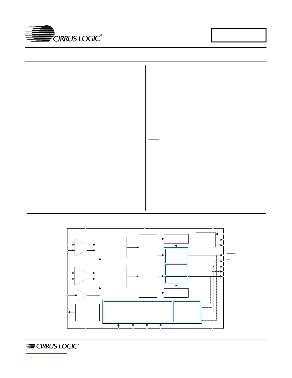
PGA
VA+
IIN+
IIN-
VIN+
VIN-
VREFIN
VREFOUT
High Pass
Filter
Voltage
Reference
x1
RESET
Digital
Filter
High Pass
Filter
x10
Energy to
Pulse Rate
Converter
4th Order
Modulator
2nd Order
Modulator
Digital
Filter
x10,x50
DGND / P1
Energy
Direction
Calibration
VD+ / P7
Configuration Inputs: On-Chip Calibration,
Pulse Output Mode / Output Frequency,
HPF Option, and
Current Channel Input Range
Clock
Generator
XOUT
CPUCLK
E2 / P4
E1 / P5
FOUT / P6
IGAIN CAL1FREQ CAL0
NEG/P2
P3
XIN
Program Select
Outputs
for
Configuration
AGND
Low-cost Power/Energy IC with Pulse Output
Features
Single-chip Power Measurement Solution
Energy Data Linearity: ±0.1% of Reading over
1000:1 Dynamic Range
On-chip functions: Measures Energy and
Performs Energy-to-Pulse Conversions
Meets Accuracy Spec for IEC 687/1036
On-chip System Calibration Option
High-pass Filter Option for Both I and V
2 Available Current Input Ranges
On-chip 2.5 V Reference (25 ppm/°C typ)
Pulse Outputs for Stepper Motor or Mechanical
Counter
On-chip Energy Direction Indicator
Ground Reference Input Signals with Single
Supply
High-frequency Output for Calibration
On-chip Power-on Reset
Power Supply Configurations:
VA+ = +5 V; AGND = 0 V; VD+ = +3.3 V to 5 V
I
Description
The CS5462 is a low-cost power meter solution
combining two analog-to-digital convertersADCs),
an energy-to-frequency converter, and energy pulse
outputs on a single chip. It is designed to accurately
measure and calculate energy for single-phase 2- or 3wire power metering applications with minimal external
components.
Low-frequency energy outputs, E1
average real power and can be used to drive a stepper
motor or a mechanical counter; the high-frequency
energy output FOUT
NEG
indicates negative power.
can be used for calibration; and
The CS5462 has configuration pins which allow for direct
configuration of pulse output format, pulse output
frequency, current channel input range, high-pass filter
option, and on-chip calibration.
The CS5462 also has a power-on reset function which
holds the part in reset until the supply reaches an
operable level.
ORDERING INFORMATION:
See page 16.
and E2, supply
http://www.cirrus.com
Copyright Cirrus Logic, Inc. 2011
(All Rights Reserved)
APR 11
DS547F1
Page 2

TABLE OF CONTENTS
1. GENERAL DESCRIPTION .......................................................................................................3
2. PIN DESCRIPTION ...................................................................................................................3
3. CHARACTERISTICS/SPECIFICATIONS ................................................................................. 5
ANALOG CHARACTERISTICS................................................................................................5
DIGITAL CHARACTERISTICS.................................................................................................7
SWITCHING CHARACTERISTICS ..........................................................................................7
ABSOLUTE MAXIMUM RATINGS ........................................................................................... 8
3.1 Theory of Operation ......................................................... .... ... ........................................... 9
3.1.1 Digital Filters ............. .... ... ... ... ....................................... ... ... .... ... ...........................9
3.1.2 Gain Calibration .................. ... ... .... ... ....................................... ... ... ... .... ... ... ... ........9
3.1.3 Energy-to-Frequency Conversion .......... .... ... ... ... .... ... ... ... ... .... ... ... ... .... .................9
4. FUNCTIONAL DESCRIPTION ...............................................................................................10
4.1 Programmable Gain Amplifier (PGA) ............................................................................... 10
4.2 Pulse-Rate Output ..................................... ... ...................................................................10
4.2.1 Stepper Motor Format. ........................................................................................10
4.2.2 Mechanical Counter Format ................................................................................ 11
4.3 Energy Direction Indicator ................................................................................................11
4.4 Internal Calibration Option ...............................................................................................11
4.5 Power-on Reset ............................ ... ... ....................................... ... ... .... ... ... ... .... ...............11
4.6 Oscillator Characteristics .................... ... .... ... ... ... .... ... ... .......................................... ... ... ...12
4.7 User Defined Settings .......................................................... ... ... ......................................12
4.8 Basic Application Circuit Configurations .......................................................................... 14
5. PACKAGE DIMENSIONS ....................................................................................................... 15
6. ORDERING INFORMATION .................................................................................................. 16
7. ENVIRONMENTAL, MANUFACTURING, & HANDLING INFORMATION ............................ 16
8. REVISIONS ............................................................................................................................. 16
CS5462
LIST OF FIGURES
Figure 1. Data Flow......................................................................................................................... 9
Figure 2. PGA Settings..................................................................................................................10
Figure 3. Pulse Output Settings ....................................................................................................10
Figure 6. Calibration Options......................................................................................................... 11
Figure 7. Power-on Reset .............................................................................................................12
Figure 8. Oscillator Connection.....................................................................................................12
Figure 9. Calibration, Frequency Select, and PGA Select ............................................................12
Figure 7. Power-on Reset .............................................................................................................13
Figure 8. Typical Connection Diagram..........................................................................................14
2 DS547F1
Page 3
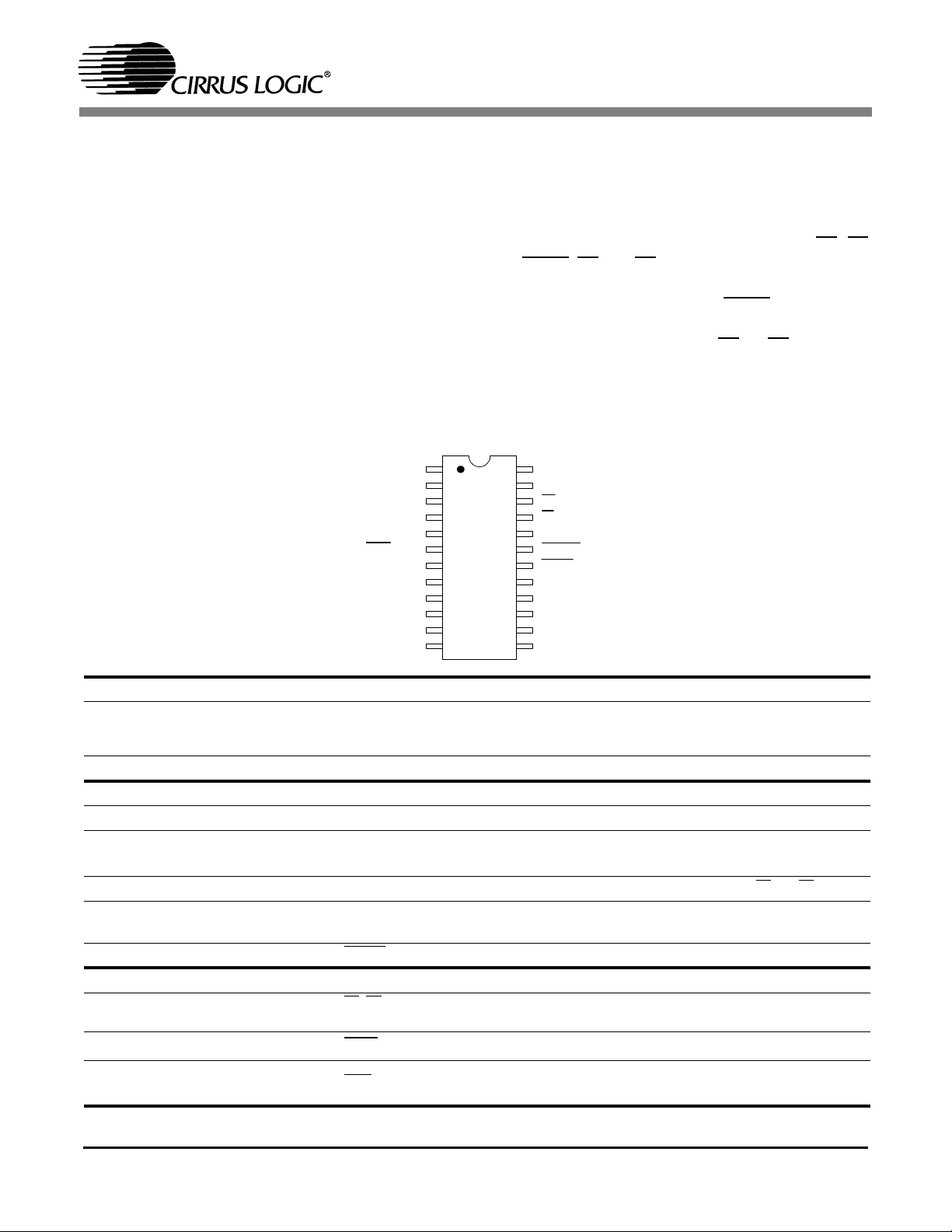
CS5462
VREFIN 12Voltage Reference Input
VREFOUT 11Voltage Reference Output
VIN- 10Differenti al Voltage Input
VIN+ 9Differenti al Voltage Input
DGND 8Digital Ground
FREQ 7Frequency Select
NEG / P2 6Neg Energy Indi c ator / Prog Sel 2
CAL0 5Calibrat ion Pin 0
DGND / P1 4Digital Ground / Pr og S el 1
VD+ / P7 3Positive Power Supply / P r og Se l 7
CPUCLK 2CPU Clock Output
XOUT 1Crystal Out
AGND13 Analog Ground
VA+14 Positive Analog Supply
IIN-15 Different i al Current Input
IIN+16 Different i al Current Input
IGAIN17 Gain Select
FOUT / P618 High Frequency Output / Prog Sel 6
RESET19 Reset
P320 Program Select 3
E1 / P521 Energy Output 1 / Prog Sel 5
E2 / P422 Energy Output 2 / Prog Sel 4
CAL123 Calibr ation Pin 1
XIN24 Crystal In
1. GENERAL DESCRIPTION
The CS5462 is a CMOS monolithic power measurement device with an energy computation engine. The CS5462 combines a programmable gain
amplifier, two ADC’s, system calibration, and
energy-to-frequency conversion circuitry on a single chip.
The CS5462 is designed for energy measurement
applications and is optimized to interface to a shunt
or current transformer for current measurement,
and to a resistive divider or transformer for voltage
measurement. The current channel has a pro-
2. PIN DESCRIPTION
grammable gain amplifier (PGA) which provides
two full-scale input level options. With a single +5 V
supply on VA+/AGND, both of the CS5462’s input
channels accommodate common mode + signal
levels between (AGND - 0.25 V) and VA+.
The CS5462 has three pulse output pins: E1
, E2
and FOUT. E1 and E2 can be used to directly drive
a mechanical counter or stepper motor, or interface to a microcontroller. The FOUT
pin conveys
average real power at a pulse frequency many
times higher than that of the E1
or E2 pulse fre-
quency, allowing for high speed calibration.
Clock Generator
Crystal Out
Crystal In
CPU Clock Output 2
Control Pins
Calibration Pins 5, 23
Program
Selects
Frequency Select 7
Current Channel Gain
Select
Reset 19
Energy Pulse Outputs
Energy Output 1
High Freq Output
Negative Energy
Indicator
1,2,3,4,5,6
6
4
3
, 2
5
DS547F1 3
1,24
4,6,20,22,21,
18,3
17
21, 22
18
6
XOUT, XIN - A single stage amplifier inside the chip is connected to these pins and can be used
with a crystal to provide the system clock for the device. Alternatively, an external clock can be
supplied to the XIN pin to provide the system clock for the device.
CPUCLK - Output of on-chip oscillator which can drive one standard CMOS load.
CAL0, CAL1 - Must be tied to a program select pin for calibration.
P1, P2, P3, P4, P5, P6, P7 - Used in Calibration, Frequency Select, and Input Gain Select.
FREQ - Must be tied to a program select pin to determine the frequency of E1 and E2.
IGAIN - Must be tied to a program select pin to determine the Full-Scale Input Voltage Range of
the current channel.
RESET - Low activates Reset
E1, E2 - The energy output pin issues a fixed-width pulse train output with a rate proportional to
real energy.
FOUT - Outputs energy pulses at a maximum rate of 10 kHz. Used for calibration purposes.
NEG - Low indicates negative energy.
Page 4

Analog Inputs/Outputs
Differential
9,10
Voltage Inputs
Voltage
11
Reference Output
Voltage
12
Reference Input
Differential
16,15
Current Inputs
Power Supply Connections
Positive
Digital Supply
Digital Ground 4*
Analog Ground 13
Positive
14
Analog Supply
CS5462
VIN+, VIN- - Differential analog input pins for voltage channel.
VREFOUT - The on-chip voltage reference is output from this pin. The voltage reference has a
nominal magnitude of 2.5 V and is referenced to the AGND pin on the converter.
VREFIN - The voltage input to this pin establishes the voltage reference for the on-chip modula-
tor.
IIN+, IIN- - Differential analog input pins for current channel.
3
VD+ - The positive digital supply.
DGND - Digital Ground
AGND - Analog Ground
VA+ - The positive analog supply.
Notes: 1 Pin number 4 is described as Digital Ground (DGND) and also P1
2
Pin number 3 is described as Positive Power Supply (VD+) and also P7
3
Pin number 22 is described as Energy Output 2 (E2) and also P4
4
Pin number 21 is described as Energy Output 1 (E1) and also P5
5
Pin number 18 is described as High Frequency Output (FOUT) and also P6
6
Pin number 6 is described as Negative Energy Indicator (NEG) and also P2
4 DS547F1
Page 5
CS5462
3. CHARACTERISTICS/SPECIFICATIONS
• Min / Max characteristics and specifications are
guaranteed over all Operating Conditions.
• Typical characteristics and specificat ions are measured at nominal supply voltages and T
= 25 °C.
A
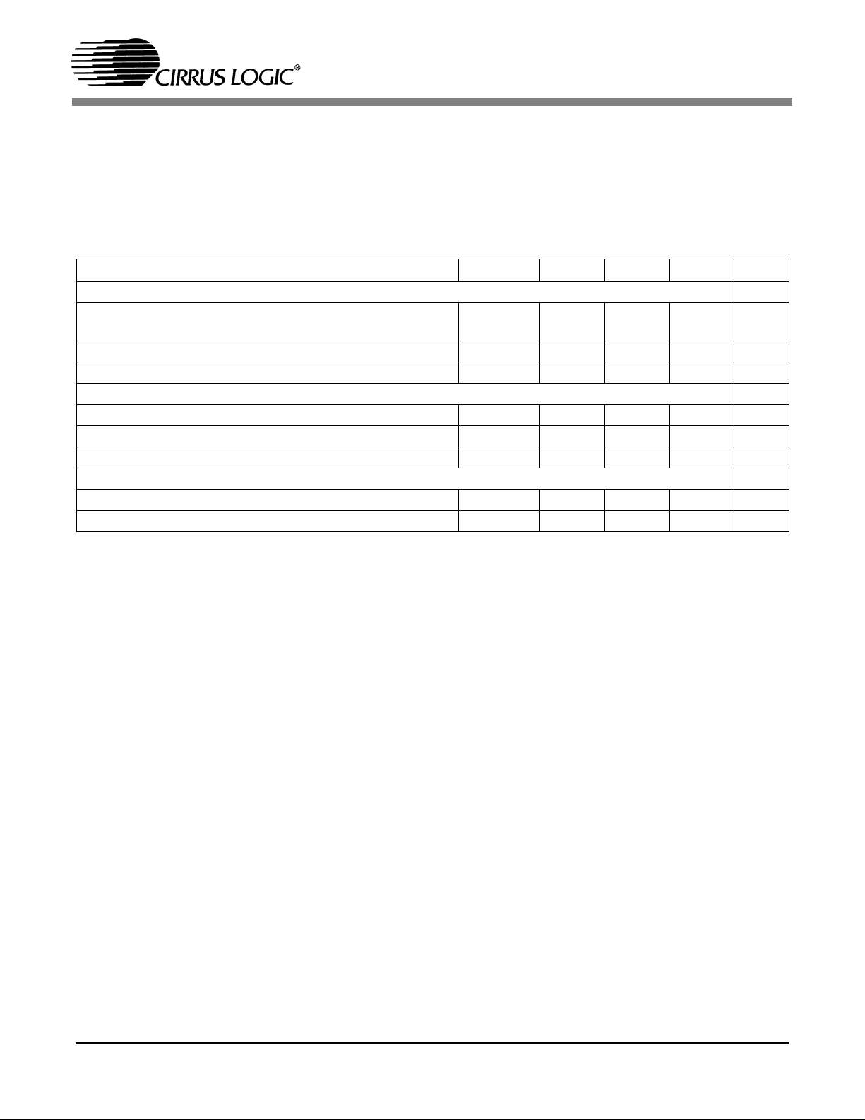
ANALOG CHARACTERISTICS
Parameter Symbol Min Typ Max Unit
Analog Inputs (Current Channel)
Maximum Differential Input Voltage Range (Gain = 10)
{(I
IN+)-(IIN-)} (Gain = 50)
Input Capacitance (All Gain Ranges) CinI -25-pF
Effective Input Impedance (All Gain Ranges)(Note 2) Z
Analog Inputs (Voltage Channel)
Maximum Differential Input Voltage Range {(V
Input Capacitance CinV -0.2-pF
Effective Input Impedance (Note 2) Z
Accuracy (Energy Outputs)
Offset Error VOS - .01 - %F.S.
Full-Scale Error (Note 1) FSE - .1 - %F.S.
IN+)-(VIN-)} VIN --500mV
• AGND = DGND = 0 V. All voltages with respect to
0V.
• CAL0 and CAL1 are connected to P4 unless otherwise noted.
IN -
I
-
inI 30 - - k
inV 5--M
-
-
500
100
mV
mV
P-P
P-P
P-P
Notes: 1. Applies After System Calibration
2. VA+ = VD+ = 5 V ±10 %; MCLK = 4.096 MHz
DS547F1 5
Page 6

CS5462
PSRR 20
0.150V
V
eq
----------------- -
log=
(VREFOUTMAX - VREFOUTMIN)
VREFOUT
AVG
(
(
1
T
A
MAX
- T
A
MIN
(
(
1.0 x 10
(
(
6
TC
VREF
=
ANALOG CHARACTERISTICS (Continued)
Parameter Symbol Min Typ Max Unit
Dynamic Characteristics
High Pass Filter Pole Frequency -3 dB - 0.5 - Hz
Power Supplies
Power Supply Currents I
I
(VD+ = 5 V)
D+
(VD+ = 3.3 V)
I
D+
Power Consumption (VD+ = 5 V)
(Note 3) (VD+ = 3.3 V)
Power Supply Rejection Ratio (50, 60 Hz)
(Note 4) Voltage Channel (Gain = 10)
Current Channel (Gain = 10)
(Gain = 50)
Notes: 3. All outputs unloaded. All inputs CMOS level.
Definition for PSRR: VREFIN tied to VREFOUT, VA+ = VD+ = 5 V, a 150 mV zero-to-peak sine wave (frequency
4.
= 60 Hz) is imposed onto the +5 V supply voltage at VA+ and VD+ pins. The “+” and “-” input pins of both input
channels are shorted to VA-. Then the CS5462 is put into an internal test mode and digital output data is collected
for the channel under test. The zero-peak value of the digital sinusoidal output signal is determined, and this value
is converted into the zero-peak value of the sinusoidal voltage that would need to be applied at the channel’s inputs,
in order to cause the same digital sinusoidal output. This voltage is then defined as Veq. PSRR is then (in dB):
A+
PSCA
PSCD
PSCD
PC -
PSRR
PSRR
PSRR
48
75
56
-
-
-
-
1.3
2.9
1.7
21
11.6
-
-
-
-
25
-
-
-
-
-
-
-
-
mA
mA
mA
mW
mW
dB
dB
dB
VREFOUT REFERENCE OUTPUT VOLTAGE
Parameter Symbol Min Typ Max Unit
Reference Output
Output Voltage REFOUT +2.4 +2.6 V
VREFOUT Temperature Coefficient TC
Load Regulation (Output Current 1 A Source or Sink) V
Reference Input
Input Voltage Range VREFIN +2.4 +2.5 +2.6 V
Input Capacitance - 4 - pF
Input CVF Current - 25 - nA
Notes: 5. The voltage at VREFOUT is measured across the temperature range. From these measurements the
following formula is used to calculate the VREFOUT Temperature Coefficient:.
VREF 25 60 ppm/°C
R
610mV
6 DS547F1
Page 7

DIGITAL CHARACTERISTICS (Note 6)
Parameter Symbol Min Typ Max Unit
High-Level Input Voltage
XIN
RESET
Low-Level Input Voltage (VD = 5 V)
XIN
RESET
Low-Level Input Voltage (VD = 3.3 V)
XIN
RESET
High-Level Output Voltage (except XOUT) I
Low-Level Output Voltage (except XOUT) I
Input Leakage Current I
Digital Output Pin Capacitance C
Drive Current FOUT
, E1, E2, NEG, CPUCLK 90 mA
Notes: 6. All measurements performed under static conditions.
= +5 mA V
out
= -5 mA V
out
CS5462
V
IH
V
IL
V
IL
OH
OL
in
out
(VD+) - 0.5
0.8VD+
-
-
-
-
-
-
-
-
-
-
-
-
1.5
0.2VD+
0.3
0.2VD+
(VD+) - 1.0 - - V
--0.4V
-±1±10µA
-5-pF
V
V
V
V
V
V
SWITCHING CHARACTERISTICS
Parameter Symbol Min Typ Max Unit
Master Clock Frequency Internal Gate Oscillator MCLK 3 4.096 5 MHz
Master Clock Duty Cycle 40 - 60 %
CPUCLK Duty Cycle (Note 7) 40 60 %
Rise Times Any Digital Input
(Note 8) Any Digital Output
Fall Times Any Digital Input
(Note 8) Any Digital Output
Start-up
Oscillator Start-Up Time XTAL = 4.096 MHz (Note 9) t
7. If external MCLK is used, then the duty cycle must be between 45% and 55% to maintain this
specification.
8. Specified using 10% and 90% points on wave-form of interest. Output loaded with 50 pF.
9. Oscillator start-up time varies with crystal parameters. This specification does not apply when using an
external clock source.
t
t
rise
fall
ost
-
-
-
-
50
50
-
-
1.0
-
1.0
-
µs
ns
µs
ns
-60-ms
DS547F1 7
Page 8

ABSOLUTE MAXIMUM RATINGS
WARNING: Operation at or beyond these limits may result in permanent damage to the device.
Normal operation is not guaranteed at these extremes.
Parameter Symbol Min Typ Max Unit
DC Power Supplies (Notes 10, 10 and 12)
Positive Digital
Positive Analog
Input Current, Any Pin Except Supplies (Notes 13, 14, 15) I
Power Dissipation (Note 16) P
Analog Input Voltage All Analog Pins V
Digital Input Voltage All Digital Pins V
Ambient Operating Temperature T
Storage Temperature T
10. VA+ and AGND must satisfy {(VA+) - (AGND)} + 6.0 V.
11. VD+ and AGND must satisfy {(VD+) - (AGND)}
12. VA+ and VD+ can differ by as much as 200 mV, as long as VA+ > VD+.
13. Applies to all pins including continuous over-voltage conditions at the analog input pins.
14. Transient current of up to 100 mA will not cause SCR latch-up.
15. Maximum DC input current for a power supply pin is ±50 mA.
16. Total power dissipation, including all input currents and output currents.
VD+
VA+
IN
D --500mW
INA
IND
A
stg
+ 6.0 V.
-0.3
-0.3
-
-
--±10mA
- 0.3 - (VA+) + 0.3 V
-0.3 - (VD+) + 0.3 V
-40 - 85 °C
-65 - 150 °C
CS5462
+6.0
+6.0
V
V
8 DS547F1
Page 9

CS5462
x
VIN±
IIN±
PGA Gain Select
HPF Select
Freq Select
Energy to
Pulse Rate
Converter
E1
E2
FOUT
Calibration
Digital
Filters
Digital
Filters
4th Order
Modulator
2nd Order
Modulator
PGA
10x
x
On-Chip
Configuration
Output Mode Select
HPF
HPF
Figure 1. Data Flow
3.1 Theory of Operation
A computational flow diagram for the two data
paths is shown in Figure 1. The analog waveforms
at the voltage/current channel inputs are subject to
the gains of the input PGAs.
3.1.1 Digital Filters
The modulators convert the analog input voltages
on the I and V channels to a digital bitstream; which
is then filtered by the digital filter section. The digital filter is composed of low pass sinc
3
and IIR filters. The IIR filters are used to compensate for the
magnitude roll-off of the low pass filter section.
Both channels provide a high-pass filter option
which can be engaged into the signal path to remove the DC content from the current/voltage signal
before the energy calculations are made.
3.1.2 Gain Calibration
After being filtered, the instantaneous voltage and
current digital codes are used to calculate real av-
erage power. This power is then adjusted based on
the internal calibration setting defined at startup.
Calibrating the CS5462 is done by externally connecting the configuration input pins, CAL1 and
CAL0, to the program select output pins, P1 - P7,
in a particular sequence. These connections will internally compensate for small gain errors.
3.1.3 Energy-to-F requency Conversion
The calibrated energy value is then converted into
a pulse output stream with a average frequency
proportional to the measured energy. Pulse output
pins E1
directly drive a stepper motor or a mechanical
counter or interface a microcontroller or infrared
LED. The FOUT
quency of 10 kHz. With full scale inputs on both the
current and voltage channels FOUT
pulses with an average frequency of 10 kHz.
and E2 can be set to lower frequencies to
pulse output pin is set to max fre-
will output
DS547F1 9
Page 10

CS5462
IGAIN
500mV
P-P
10xP1
P2
P3
P4
P5
100mV
P-P
50x
500mV
P-P
10x
100mV
P-P
50x
P6
P7
500mV
P-P
10x
100mV
P-P
50x
500mV
P-P
10x
no hpf
no hpf
hpf both
hpf both
hpf Ich
hpf Ich
hpf Vch
Figure 2. PGA Settings
FREQ
0.25 Hz / StepP1
P2
P3
P4
P5
0.5 Hz / Step
1 Hz / Step
2 Hz / Step
4 Hz / Step
P6P72 Hz / mech cnt
16 Hz / mech cnt
Figure 3. Pulse Output Settings
0.25 Hz 0.5 Hz
250 ms 250 msPulse Width
Frequency
P1 P2
FREQ
connected to:
1 Hz 2 Hz
250 ms 250 ms
P3 P4
4 Hz
125 ms
P5
E1
pulse width
E2
4. FUNCTIONAL DESCRIPTION
4.1 Programmable Gain Amplifier (PGA)
The CS5462 is equipped with a PGA on the current
channel. While the voltage channel is always set to
a 10x differential input voltage range (500 mV
the current channel can be set to one of two different input ranges. The maximum differential voltage
range on the current channel can be set to 10x
(500 mV
The gain setting of the current channel’s PGA and
also the high pass filter option are selected by connecting the IGAIN pin to one of seven Program Select output pins. For all applications the IGAIN pin
must be tied to one and only one Program Select
pins. Figure 2 below shows the different options
that can be selected at startup. These seven differ-
ent options allow the CS5462’s PGA to be set up in
either 10x or 50x mode and enable or disable the
high pass filters in either of the voltage or the current channels.
During Startup the CS5462 will scan the IGAIN input pin and determine which Program Select output it is connected to and then set the PGA and
HPF’s accordingly.
4.2 Pulse-Rate Output
E1 and E2 pins provide a simple interface from
which signed energy can be accumulated. E1
E2
chanical counter mode. The connectivity of the
FREQ pin determines the pulse output mode and
10 DS547F1
P-P
) and 50x (100 mV
P-P
P-P
).
and
can be set to either stepper motor mode or me-
also the maximum frequency for E1
3 below describes the options for E1
and E2. Figure
and E2.
),
For all applications FREQ must be connected to
one and only one of the Program Selects outputs
(P1 - P7). The frequency setting chosen using the
above table is equal to the set pulse rate frequency
if and only if a full-scale signal is applied to each
channel. As the input signal decreases the pulse
rate and pulse width will decrease by a percentage
equal to the product of the percentages of fullscale inputs across each channel. For example, if
if FREQ is connected to P5, the maximum pulse
output rate is 4 Hz. Assuming 500 mV is selected
as full scale on each channel, 400 mV is measured
on current and voltage channels. 400 mV is 80% of
full scale. Since power is the product of current and
voltage the pulse outputs will be 80% * 80% = 64%
of full scale. Since 4 Hz is the set full scale output
rate, pulses should appear on E1
and E2 at a
64% * 4 Hz = 2.56 Hz rate.
4.2.1 Stepper Motor Format.
In stepper motor mode the CS5462 produces alternating pulses on E1
designed to directly drive a stepper motor. Each
pin produces active-low pulses with frequency dependent pulse widths. The figure below shows the
frequency and corresponding pulse width for each
option.
and E2. This pulse format is
Page 11

pulse width
E1
pulse width
Positive Energy Negative Energy
E2
2 Hz 16 Hz
125 ms 15 msPulse Width
Frequency
P6 P7
FREQ
connected to:
CAL1
+4.2%P1
P2
P4
P6
P7
+2.8%
0%
-2.8%
-4.2%
CAL0
+0.6%
+0.4%
0%
-0.4%
-0.6%
P3
P5
+1.4%
-1.4%
+0.2%
-0.2%
Figure 6. Calibration Options
CS5462
4.2.2 Mechanical Counter Format
In mechanical counter mode, the CS5462 produces pulses on E1
a bi-directional mechanical counter. Each pin produces active-low pulses which have pulse widths
of 125 ms or 15 ms, depending on the frequency
selected. In the figure below, the frequency and
corresponding pulse width is shown for each option available. In this mode when energy is positive, the pulses appear on E1
negative, pulses appear on E2
4.3 Energy Direction Indicator
For either pulse output mode, the NEG pin can be
used to indicate the direction of the energy calculated. The NEG
of the converter. If negative energy is detected the
NEG
pin will become active low and will remain ac-
tive low until positive energy is detected.
4.4 Internal Calibration Option
For most power meter applications the standard
accuracy requirements require the meter be calibrated to within a certain percentage. Calibrating a
CS5462 meter can be done a number of ways.
One calibration method is to externally adjust the
front-end input circuit by using a potentiometer or
resistor network. By adjusting the amount of gain in
the resistor divider on the front end the energy outputs can be adjusted to fit the accuracy required.
Although this method is available, it may be costly
to add the additional components and the accuracy
required is often difficult to achieve. As an alternative the CS5462 is designed to allow the user to
calibrate the part without the need for external potentiometers or resistor networks. The CS5462
provides a digital on-chip calibration solution. This
digital alternative can calibrate energy registration
error to within 0.1% without any analog adjustments.
DS547F1 11
and E2 which can be used to drive
; when energy is
.
pin is updated at the sample rate
This calibration is accomplished by connecting
each Configuration Input pin, CAL1 and CAL0, to
one of the Program Select Output pins, P1 - P7. At
startup the CS5462 will scan the CAL1 and CAL0
pins to discern what connections are made, and
then calibrate the gain accordingly.
CAL1 and CAL0 each have seven options which
allows for 49 different steps of 0.2% between
+4.8% and -4.8% of expected energy output. Before startup, CAL1 and CAL0 must each be connected to only one of the program select pins.
To Calibrate the CS5462:
1. Connect CAL1 and CAL0 to P4. This connection
will adjust the energy outputs by 0%.
2. Apply known current and voltage signals to the
inputs of the CS5462.
3. Measure the average pulse output frequency of
FOUT
, E1, or E2.
4. The average frequency will be within some percentage of the expected frequency. Depending on
the output of the uncalibrated chip, the CAL0 and
CAL1 pins can be adjusted using the above options
(see “User Defined Settings” on page 12 for more
on calibration).
4.5 Power-on Reset
The CS5462 is equipped with internal circuitry that
will put the chip into reset if power supply is lost.
This is particularly useful in black-out or brown-out
situations in which the power supply temporarily interrupted. The CS5462 will enter into reset if the
power drops below 2.5 V. The chip will remain in
reset until the supply rises to 4 V (See Figure 6) at
Page 12

CS5462
Reset Reset
Normal
Operation
5 V
4 V
2.5 V
1 V
0 V
Time
Supply
Voltage
Figure 7. Power-on Reset
Oscillator
Circuit
DGND
XIN
XOUT
C1
C1 = 22 pF
C2
C2 =
Figure 8. Oscillator Connection
P1
P2
P3
P4
P5
P6
P7
10x
50x
10x
50x
50x
10x
10x
CAL1 CAL0
0.25 Hz (stp)
FREQ
+4.2%
+2.8%
+1.4
0
-1.4%
-2.8%
-4.2%
IGAIN
+0.6%
+0.4%
+0.2%
0
-0.2%
-0.4%
-0.6%
0.5 Hz (stp)
1 Hz (stp)
2 Hz (stp)
4 Hz (stp)
4 Hz (mc)
16 Hz (mc)
500mV
100mV
500mV
100mV
100mV
500mV
500mV
no hpf
no hpf
hpf both
hpf both
hpf Ich
hpf Vch
hpf Ich
Figure 9. Calibration, Frequency Select, and
PGA Select
which time the CS5462 will configure itself and resume normal operation.
4.6 Oscillator Characteristics
XIN and XOUT are the input and output of an inverting amplifier which can provide oscillation and
can be configured as an on-chip oscillator, as
shown in Figure 8. The oscillator circuit is designed
to work with a quartz crystal or a ceramic resonator. To reduce circuit cost, two load capacitors C1
and C2 are integrated in the device, one between
XIN and DGND, one between XOUT and DGND.
Lead lengths should be minimized to reduce stray
capacitance. To drive the device from an external
clock source, XOUT should be left unconnected
while XIN is driven by the external circuitry. There
is an amplifier between XIN and the digital section
which provides CMOS level signals. This amplifier
works with sinusoidal inputs so there are no problems with slow edge times.
12 DS547F1
4.7 User Defined Settings EXAMPLE: Design a hybrid stepper motor meter
with an 2 Hz maximum pulse output frequency on
the E1
puts of the current and voltage channels and the
high pass filter enabled on the current channel only. Using the figure below these settings can be selected with two connections.
By directly connecting FREQ with P4 and IGAIN
with P5 the CS5462 is configured to drive a stepper motor with a maximum pulse output rate of
2 Hz, to support an input range of 500 mV
to remove all DC content on the current signals by
enabling the HPFs on the Ich. The CS5462 is now
ready for calibration.
Before applying power to the chip, connect the
CAL0 and CAL1 pins to P4. This will select
0% + 0% = 0% gain adjustment. After making this
connection the CS5462 is ready to be calibrated.
Once power is applied the CS5462 will begin a
startup sequence in which it will scan the FREQ,
IGAIN, CAL0, and CAL1 pins. After determining
which connections are made the FREQ, IGAIN,
CAL0, and CAL1 pins will become high impedance
inputs and the part will begin normal operation and
start converting. If on-chip calibration is required
place known voltages across the inputs on IIN±
and VIN±.
For example, 150 mV
used for both the current and voltage inputs.
424.26 mV
scale input of both the current and voltage channels. With this input on both channels the expected
pulse output frequency is
84.853% * 84.853% = 72% of full scale. This
, E2 pins with 500 mV
= ~424.26 mV
RMS
is ~84.853% of the maximum full
P-P
signal on the in-
P-P
P-P
P-P
, and
will be
Page 13

CS5462
P3
+4.4%
+3.0%
+1.6%
+0.2%
-4.0%
-2.6%
-1.2%
+4.8%
P1
P2
P3
P4
P5
P6
P7
P1 P2 P4 P5 P6 P7
+4.6%
+3.4% +3.2%
+2.0% +1.8%
+0.0%
+0.6% +0.4%
+4.2% +4.0% +3.8%
+2.8% +2.6% +2.4%
+1.4% +1.2% +1.0%
+3.6%
+2.2%
+0.8%
CA L0 connected to:
CAL1
connected
to:
-4.8%-4.6%-4.4 %
-3.4%-3.2%-3.0 %
-2.0%
-1.8%-1.6%
-0.6%
-0.4%
-0.2%
-4.2%-3.8%
-2.8%
-2.4%
-1.4%
-1.0%
-3.6%
-2.2%
-0.8%
Figure 7. Power-on Reset
means that E1 and E2 should have an average
pulse output frequency of 2 Hz * 72% = 1.44 Hz
and FOUT
should have an average pulse output
frequency of 10 kHz * 72% = 7.2 kHz. Assuming
that FOUT
error will be the same for E1
is used for calibration (although the gain
and E2), FOUT should
be measured to find the gain error. Suppose the
measured pulse output frequency is 6.966 kHz instead of 7.2 kHz. 6.996 kHz is 96.76% of 7.2 kHz.
This means that the gain error is 96.76% 100% = -3.24%. This error can be calibrated out by
connecting CAL1 to P2 and CAL0 to P2 (see Fig-
ure 7 for all connection options). This will adjust the
pulse rate frequency by 2.8% + 0.4% = 3.2%
(since the smallest calibration step size is 0.2%,
3.2% is the closest value that can offset the error
of -3.24). After these connections are made the average pulse output frequency of FOUT
, E1, and E2
will have a gain error less than or equal to -0.04%
of full scale.
DS547F1 13
Page 14
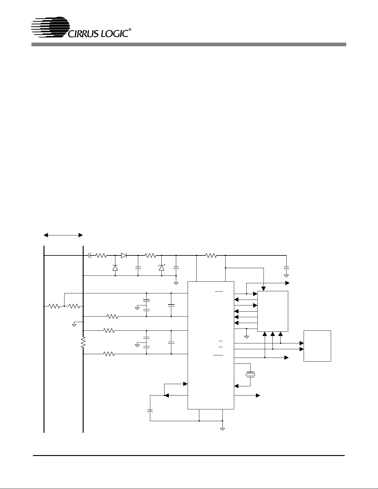
CS5462
Jumpers
for
Calibration,
Freq Select
and
Gain Select
Mechanical
Counter
DGND / P1
EDIR / P4
VD+ / P7
NEG / P2
P3
CAL0
CAL1
FREQ
IGAIN
EOUT
FOUT / P6
XOUT
XIN
CPUCLK
DGNDVA-
VREFOUT
VREFIN
IIN+
IIN-
VIN-
VIN+
AGND
3
15
14
9
10
16
12
11
13 8
2
24
1
18
21
22
17
7
5
23
20
6
4
120 VAC
nV
F F F
R
SHUNT
F
R
1
R
2
NL
AGND
VA+
E2 / P4
E1 / P5
R
I+
R
I-
R
V-
C
Idiff
C
Vdiff
C
V-
C
V+
C
I+
C
I-
Stepper
Motor
or
Figure 8. Typical Connection Diagram
4.8 Basic Application Circuit Configurations
Figure 9 shows the CS5462 configured to measure
power in a single-phase 2-wire system while operating in a single supply configuration. In this diagram, the shunt resistor used to monitor the line
current is connected on the “Line” (hot) side of the
power mains. In most residential power metering
applications, the power meter’s current-sense
shunt resistor is intentionally placed on the hot side
of the power mains in order to detect a subscriber’s
attempt to steal power. In this type of shunt-resistor
configuration, the common-mode level of the
CS5462 must be referenced to the hot side of the
power line. This means that the common-mode potential of the CS5462 will typically oscillate to very
high voltage levels, as well as very low voltage levels, with respect to earth ground potential.
14 DS547F1
Page 15

5. PACKAGE DIMENSIONS
24L SSOP PACKAGE DRAWING
E
N
1
23
e
b
2
A1
A2
A
D
SEATING
PLANE
E1
1
L
SIDE VIEW
END VIEW
TOP VIEW
INCHES MILLIMETERS NOTE
DIM MIN NOM MAX MIN NOM MAX
A -- -- 0.084 -- -- 2.13
A1 0.002 0.006 0.010 0.05 0.13 0.25
A2 0.064 0.068 0.074 1.62 1.73 1.88
b 0.009 -- 0.015 0.22 -- 0.38 2,3
D 0.311 0.323 0.335 7.90 8.20 8.50 1
E 0.291 0.307 0.323 7.40 7.80 8.20
E1 0.197 0.209 0.220 5.00 5.30 5.60 1
e 0.022 0.026 0.030 0.55 0.65 0.75
L 0.025 0.03 0.041 0.63 0.75 1.03
0° 4° 8° 0° 4° 8°
CS5462
JEDEC #: MO-150
Controlling Dimension is Millimeters.
Notes: 1. “D” and “E1” are reference datums and do not included mold flash or protrusions, but do include mold
mismatch and are measured at the parting line, mold flash or protrusions shall not exceed 0.20 mm per
side.
2. Dimension “b” does not include dambar protrusion/intrusion. Allowable dambar protrusion shall be
0.13 mm total in excess of “b” dimension at maximum material condition. Dambar intrusion shall not
reduce dimension “b” by more than 0.07 mm at least material condition.
3. These dimensions apply to the flat section of the lead between 0.10 and 0.25 mm from lead tips.
DS547F1 15
Page 16

CS5462
Contacting Cirrus Logic Support
For all product questions and inquiries contact a Cirrus Logic Sales Representative.
To find the one nearest to you go to www.cirrus.com
IMPORTANT NOTICE
Cirrus Logic, Inc. and it s su bsi di ari e s ( “Ci rr us ”) bel i eve t hat the in for mat i on c ont ai ned i n t his doc ument i s acc ur at e and re l i abl e . Howe v er, th e in fo rmation is subject
to change without not ice and is provi ded “AS IS” wit hout warr anty of any kind (express or implied). Customers are advised to obtain the latest version of relevant
information to verify, before placing orde rs, that in forma tion bei ng rel ied on is curren t and com ple te. All prod ucts are so ld su bject to the terms and cond itions of sale
supplied at the time of order acknowledgment, including those pertaining to warranty, indemnification, and limitation of liability. No responsibility is assu med by Cirrus
for the use of this information, including use of this informa tion as the basis for m anufactur e or sale of any items, or for infringe ment of patents or oth er rights of third
parties. This document is the property of Cirrus and by furnishing this information, Cirru s gr an ts no license, express or implied under an y pa ten ts, m ask wor k r ights,
copyrights, trademarks, trade secrets or other intell ectual proper ty rights. Cirrus owns the cop yrights associated with the inform ation conta ined here in and g ives consent for copies to be made of the information only for use within your organization with respect to Cirrus integrated circuits or other products of Cirrus. This consent
does not extend to other copying such as copying for ge ne ral distribution, advertising or promotional purposes, or for creating any work for resale.
CERTAIN APPLICATIONS USING SEMICONDUCTOR PRODUCTS MAY INVOLVE POTENTIAL RISKS OF DEATH, PERSONAL INJURY, OR SEVERE PROPERTY OR ENVIRONMENTAL DAMAGE (“CRITICAL APPLICATIONS”). CIRRUS PRODUCTS ARE NOT DESIGNED, AUTHORIZED OR WARR ANTED FOR USE
IN PRODUCTS SURGICALLY IMPLANTED INTO THE BODY, AUTOMOTIVE SAFETY OR SECURITY DEVICES, LIFE SUPPORT PRODUCTS OR OTHER CRITICAL APPLICATIONS. INCLUSION OF CIRRUS PRODUCTS IN SUCH APPLICATIONS IS UNDERSTOOD TO BE FULLY AT THE CUSTOMER'S RISK AND CIRRUS DISCLAIMS AND MAKES NO WARRANTY, EXPRESS, STATUTORY OR IMPLIED, INCLUDING THE IMPLIED WARRANTIES OF MERCHANTABILITY AND
FITNESS FOR PARTICULAR PURPOSE, WITH REGARD TO ANY CIRRUS PRODUCT THAT IS USED IN SUCH A MANNER. IF THE CUSTOMER OR CUSTOMER'S CUSTOMER USES OR PERMITS THE USE OF CIRRUS PRODUCTS IN CRITICAL APPLICATIONS, CUSTOMER AGREES, BY SUCH USE, TO FULLY
INDEMNIFY CIRRUS, ITS OFFICERS, DIRECTORS, EMPLOYEES, DISTRIBUTORS AND OTHER AGENTS FROM ANY AND ALL LI ABI LITY, INCLUDI NG ATTORNEYS' FEES AND COSTS, THAT MAY RESULT FROM OR ARISE IN CONNECTION WITH THESE USES.
Cirrus Logic, Cirrus, and the Cirrus Logic logo designs are trademarks of Cirrus Logic, Inc. All other br and and product names in this document may be trademarks
or service marks of their respective owners.
6. ORDERING INFORMATION
Model Temperature Package
CS5462-ISZ (lead free) -40 to +85 °C 24-pin SSOP
7. ENVIRONMENTAL, MANUFACTURING, & HANDLING INFORMATION
Model Number Peak Reflow Temp MSL Rating* Max Floor Life
CS5462-ISZ (lead free) 260 °C 3 7 Days
* MSL (Moisture Sensitivity Level) as specified by IPC/JEDEC J-STD-020.
8. REVISIONS
Revision Date Changes
A1 MAR 2003 Initial Release
PP1 OCT 2003 Initial release for Preliminary Product Information
F1 APR 2011 Removed lead-containing (Pb) device ordering information. Added MSL data.
16 DS547F1
 Loading...