

Page 1
CS5451A
VREFIN
VREFOUT
IIN1+
IIN1-
VIN1+
VIN1-
VIN2+
VIN2-
VIN3+
VIN3-
IIN2+
IIN2-
IIN3+
IIN3-
VA+
VD+
AGND
SE
FSO
SDO
SCLK
Voltage
Reference
Serial
Interface
RESET
Decimation Filter
Decimation Filter
Decimation Filter
Decimation Filter
Decimation Filter
Decimation Filter
x1, 20
x1
4th Order Modulator
x1
x1,20
x1
x1,20
x1
4th Order Modulator
4th Order Modulator
4th Order Modulator
4th Order Modulator
4th Order Modulator
GAIN
CPD
OWRS
XIN
DGND
VA-
Clock
Pulse Output
Regulator
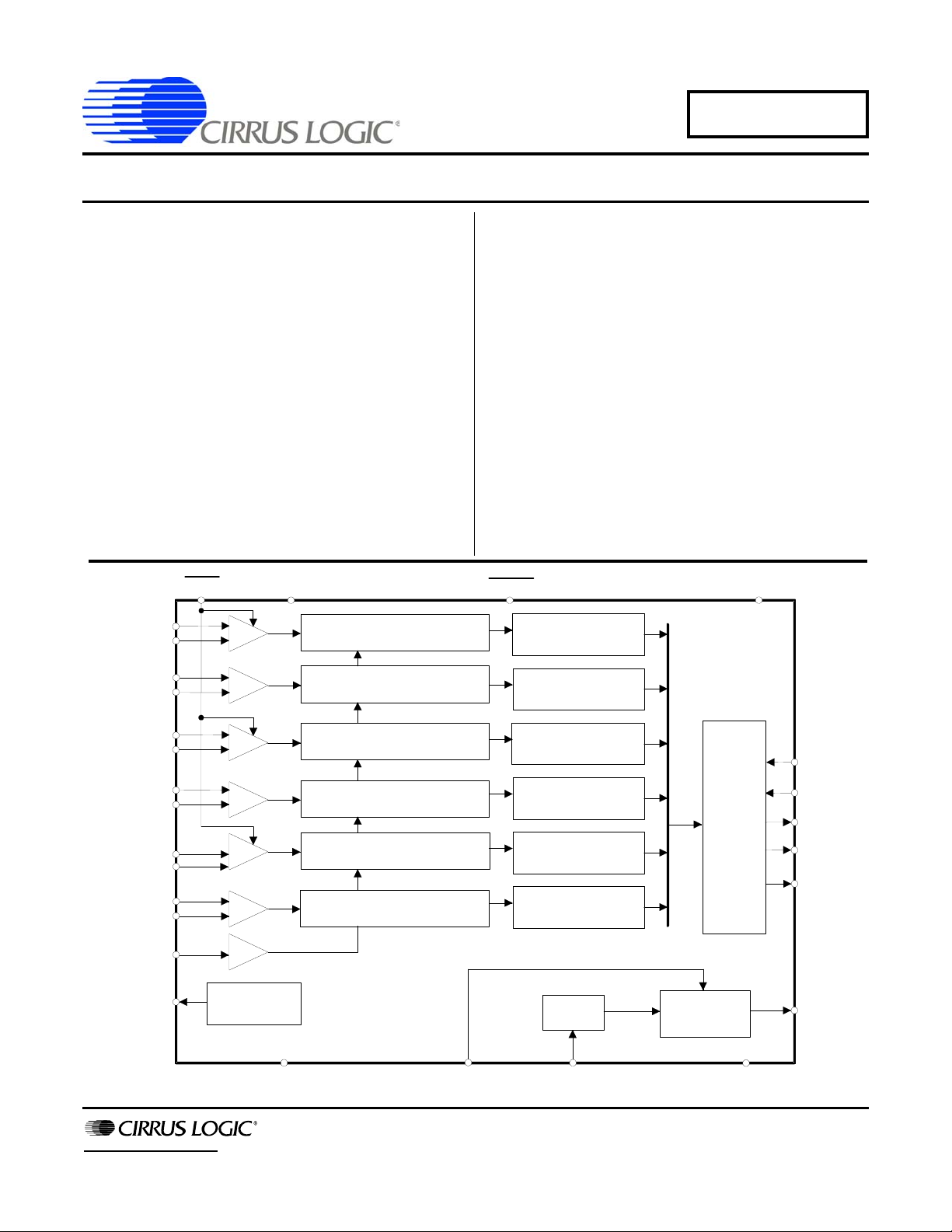
Six-channel, Delta-sigma Analog-to-digital Converter
Features
• Synchronous Sampling
• On-chip 1.2 V Reference (25 ppm/°C typ.)
• Power Supply Configurations:
- VA+ = +3 V; VA- = -2 V; VD+ = +3 V
- Supply Tolerances: ±10%
• Power Consumption
- 23 mW Typical at VD+ = +3 V
• Simple Four-wire Serial Interface
• Charge pump driver output generates
negative power supply.
• Ground-referenced Bipolar Inputs
Description
The CS5451A is a highly integrated delta-sigma ( analog-to-digital converter (ADC) developed for the power
measurement industry. The CS5451A combines six
ADCs, decimation filters, and a serial interface on a single chip. The CS5451A interfaces d irectly to a current
transformer or shunt to m eas ure curre nt, and to a resis tive divider or transformer to measure voltage. The
product features a serial interface for communication
with a microcontroller or DSP. The product is initialized
and fully functional upon reset, and includes a voltage
reference.
ORDERING INFORMATION:
See page 13.
http://www.cirrus.com
Copyright Cirrus Logic, Inc. 2011
(All Rights Reserved)
APR ‘11
DS635F4
Page 2

TABLE OF CONTENTS
1. PIN DESCRIPTION. . . . . . . . . . . . . . . . . . . . . . . . . . . . . . . . . . . . . . . . . . . . . . . . . . . . . . . . . . .3
2. CHARACTERISTICS AND SPECIFICATIONS . . . . . . . . . . . . . . . . . . . . . . . . . . . . . . . . . . . . .4
3. THEORY OF OPERATION. . . . . . . . . . . . . . . . . . . . . . . . . . . . . . . . . . . . . . . . . . . . . . . . . . . . .8
4. FUNCTIONAL DESCRIPTION . . . . . . . . . . . . . . . . . . . . . . . . . . . . . . . . . . . . . . . . . . . . . . . . . .9
4.1 Analog Inputs . . . . . . . . . . . . . . . . . . . . . . . . . . . . . . . . . . . . . . . . . . . . . . . . . . . . . . . . . . .9
4.2 Digital Filters. . . . . . . . . . . . . . . . . . . . . . . . . . . . . . . . . . . . . . . . . . . . . . . . . . . . . . . . . . . .9
4.3 Performing Measurements . . . . . . . . . . . . . . . . . . . . . . . . . . . . . . . . . . . . . . . . . . . . . . . . .9
4.4 Serial Interface . . . . . . . . . . . . . . . . . . . . . . . . . . . . . . . . . . . . . . . . . . . . . . . . . . . . . . . . . .9
4.5 System Initialization . . . . . . . . . . . . . . . . . . . . . . . . . . . . . . . . . . . . . . . . . . . . . . . . . . . . .10
4.6 Voltage Reference . . . . . . . . . . . . . . . . . . . . . . . . . . . . . . . . . . . . . . . . . . . . . . . . . . . . . .10
4.7 Power Supply . . . . . . . . . . . . . . . . . . . . . . . . . . . . . . . . . . . . . . . . . . . . . . . . . . . . . . . . . .10
5. PACKAGE DIMENSIONS. . . . . . . . . . . . . . . . . . . . . . . . . . . . . . . . . . . . . . . . . . . . . . . . . . . . .12
6. ORDERING INFORMATION . . . . . . . . . . . . . . . . . . . . . . . . . . . . . . . . . . . . . . . . . . . . . . . . . .13
7. ENVIRONMENTAL, MANUFACTURING, & HANDLING INFORMATION . . . . . . . . . . . . . . . 13
8. REVISION HISTORY . . . . . . . . . . . . . . . . . . . . . . . . . . . . . . . . . . . . . . . . . . . . . . . . . . . . . . . .13
LIST OF FIGURES
Figure 1. Serial Port Timing. . . . . . . . . . . . . . . . . . . . . . . . . . . . . . . . . . . . . . . . . . . . . . . . . . . . . . .6
Figure 2. Typical Connection Diagram . . . . . . . . . . . . . . . . . . . . . . . . . . . . . . . . . . . . . . . . . . . . . .8
Figure 3. One Data Frame . . . . . . . . . . . . . . . . . . . . . . . . . . . . . . . . . . . . . . . . . . . . . . . . . . . . . .10
Figure 4. Serial Port Data Transfer . . . . . . . . . . . . . . . . . . . . . . . . . . . . . . . . . . . . . . . . . . . . . . . .10
Figure 5. Generating VA- with a Charge Pump. . . . . . . . . . . . . . . . . . . . . . . . . . . . . . . . . . . . . . . 11
CS5451A
2 DS635F4
Page 3
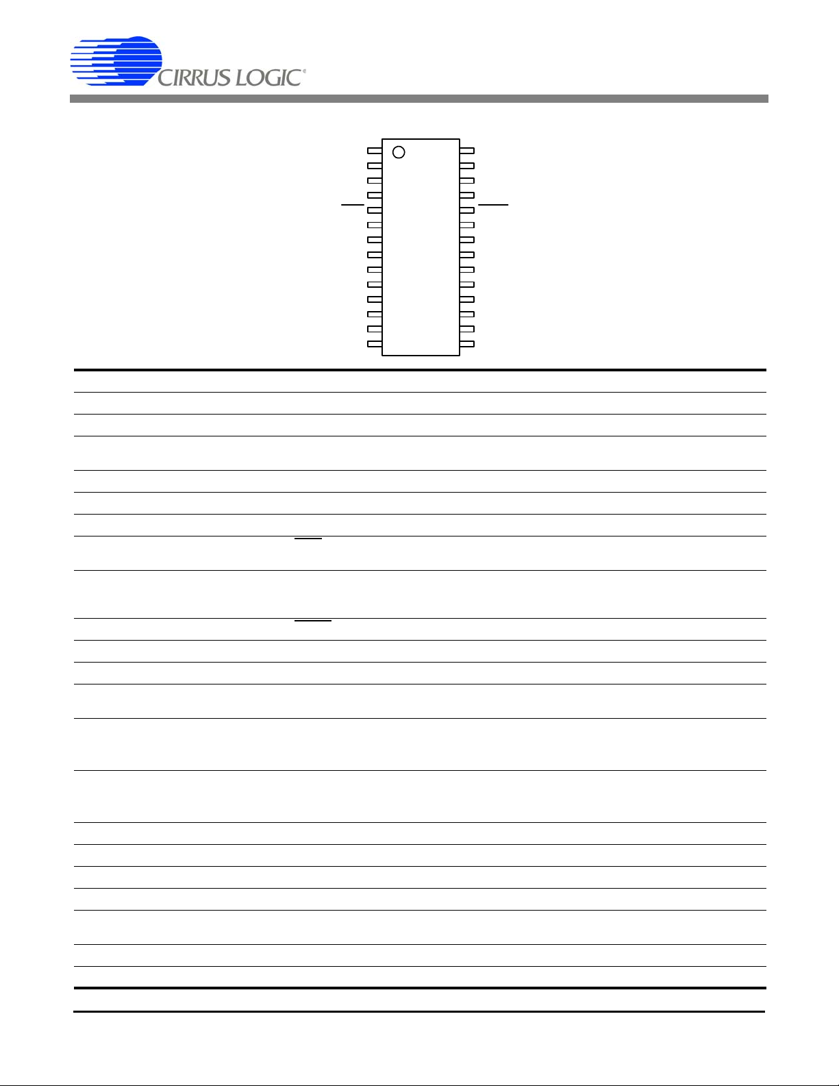
CS5451A
1
14
7
13
6
12
5
11
9
4
3
8
10
2
15
18
16
24
20
19
25
21
17
26
27
22
28
23
IIN2-
VIN2+
IIN2+
RESET
IIN1+
IIN1-
XIN
VIN1-
VIN2-
CPD
DGND
VIN1+
VD+
OWRS
IIN3-
VIN3+
IIN3+
GAIN
VA+
VA -
SE
VREFOUT
VIN3-
FSO
SDO
VREFIN
SCLK
AGND
Differential Current Input 2
Differential Volta g e Input 2
Differential Current Input 2
Reset
Differential Current Input 1
Differential Current Input 1
Master Clock
Differential Volta g e Input 1
Differential Volta g e Input 2
Charge Pump Drive
Digital Ground
Differential Volta g e Input 1
Digital Supply
Output Word Rate Select
Differential Current Input 3
Differential Voltage Input 3
Differential Current Input 3
Current Input Gain
Positive Analog Supply
Negative Analog Supply
Serial Port Enable
Reference Output
Differential Voltage Input 3
Frame Sync
Serial Data Output
Reference Input
Serial Clock Output
Analog Ground
CS5451A
1. PIN DESCRIPTION
Clock Generator
Master Clock Input 25
Control Pins and Serial Data I/O
Serial Clock Output
Serial Data Output 2
Frame Sync 3
Serial Port Enable 4
Current Input Gain
Output Word Rate Select
Reset 24
Analog Inputs/Outputs
Voltage Reference Input 7
Voltage Referenc e Outp ut
Differential V ol tage Inputs 1 1 ,12
18,17
22,21
Differential Current Inputs 13,14
16,15
20,19
Power Supply Connections
Analog Ground 6
Positive Analog Supply 9
Negative Analog Supply 10
Charge Pump Drive
Digital Ground 27
Positive Digital Supply 28
DS635F4 3
XIN - External clock signal or oscillator input.
SCLK - Serial port clock signal that determines the output data rate for SDO pin. Rate of SCLK is
1
dependent on the XIN frequency and state of OWRS pin.
SDO -Serial port data output pin. Data will be output at a rate defined by SCLK.
FSO - Framing signal indicates when data samples are about to be transmitted on the SDO pin.
SE - When SE is low, the output pins of the serial port are tri-stated.
GAIN - A logic high sets current channel gain to 1, a logic low sets the gain to 20. If no connection
5
is made to this pin, it will default to logic low level (through internal 200 k resistor to DGND).
OWRS - A logic low sets the output word rate (OWR) to XIN/2048 (Hz). A logic high sets the
OWR to XIN/1024 (Hz). If no connection is made to this pin, then OWRS will default to logic low
23
level (through internal 200 k resistor to DGND).
RESET - Low activates Reset, all internal registers are set to their default states.
VREFIN - The input to this pin establishes the voltage reference for the on-chip modulator.
VREFOUT - The on-chip voltage reference output. The voltage reference has a nominal magni-
8
tude of 1.2 V and is referenced to the AGND pin on the converter.
VIN3+, VIN3- - Differential analog input pins for the voltage channel 3.
VIN2+, VIN2- - Differential analog input pins for the voltage channel 2.
VIN1+, VIN1- - Differential analog input pins for the voltage channel 1.
IIN3+, IIN3- - Differential analog input pins for the current channel 3.
IIN2+, IIN2- - Differential analog input pins for the current channel 2.
IIN1+, IIN1- - Differential analog input pins for the current channel 1.
AGND - Analog ground.
VA+ - The positive analog supply. Typical +3 V ±10% relative to AGND.
VA- - The negative analog supply. Typical -2 V ±10% relative to AGND.
CPD - Designed to drive external charge pump circuitry that will produce a negative analog sup-
26
ply (VA-)voltage.
DGND - Digital Ground.
VD+ - The positive digital supply. Typical +3 V ±10% relative to AGND.
Page 4
CS5451A
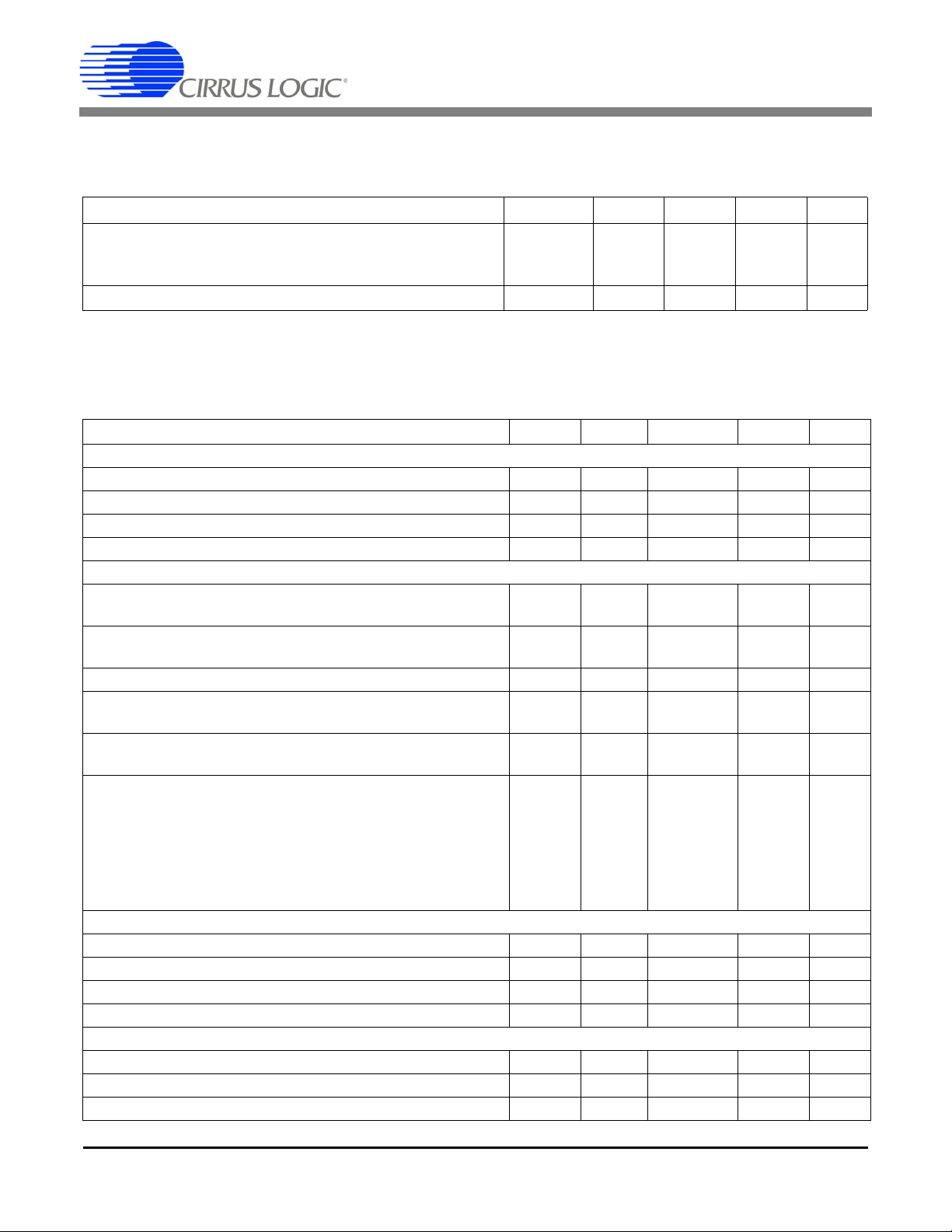
2. CHARACTERISTICS AND SPECIFICATIONS
RECOMMENDED OPERATING CONDITIONS
Parameter Symbol Min Typ Max Unit
DC Power Supplies Positive Digital
Positive Analog
Negative Analog
Voltage Reference Input VREF+ - 1.2 - V
ANALOG CHARACTERISTICS
• Min/Max characteristics and specifications are guaranteed over all Operating Conditions.
• Typical characteristics and specifications are measured at nominal supply voltages and TA = 25 °C.
• VA+ = VD+ = 3 V ±10%; VA- = -2 V ±10%; AGND = DGND = 0 V; VREFIN = +1.2 V. All voltages with respect to 0 V.
• XIN = 4.096 MHz.
Parameter Symbol Min Typ Max Unit
Accuracy (All Channels)
Total Harmonic Distortion THD 74 - - dB
Common Mode Rejection (DC, 50, 60 Hz) CMRR 80 - - dB
Common Mode + Signal on Input VA- - VA+ V
Input Sampling Rate - XIN/8 - Hz
Analog Inputs (Note 1)
Differential Input Voltage Range Gain=20
[(I
IN+) - (IIN-)] or [(VIN+) - (VIN-)] Gain=1
Bipolar Offset Gain=20
Gain=1
Crosstalk (Channel-to-channel) (50, 60 Hz) - -105 - dB
Input Capacitance Gain = 20
Gain = 1
Effective Input Impedance Gain=20
Gain=1
Noise (Referred to Input)
0-60 Hz Gain=20
Gain=1
0-1 kHz Gain=20
Gain=1
0-2 kHz Gain=20
Gain=1
Reference Output
Output Voltage REFOUT 1.15 1.2 1.25 V
Temperature Coefficient - 25 50 ppm/°C
Load Regulation (Output Current 1 A Source or Sink) V
Power Supply Rejection PSRR 60 - - dB
Reference Input
Input Voltage Range VREF+ 1.15 1.2 1.25 V
Input Capacitance - - 10 pF
Input CVF Current - - 1 µA
VD+
VA+
VA-
VIN
VIN
VOS
VOS
IC
IC
EII
EII
2.7
2.7
-2.2
-
-
-
-
-
-
50
500
-
-
-
-
-
-
R
-610mV
3.0
3.0
-2.0
80
1.6
±11.5
±0.5
-
-
60
600
-
-
-
-
-
-
3.3
3.3
-1.8
-
-
±20
±4.0
20
1
-
-
1
20
2.5
50
3.75
75
mV
V
mV
mV
µV
µV
µV
µV
µV
µV
V
V
V
P-P
P-P
pF
pF
k
k
rms
rms
rms
rms
rms
rms
4 DS635F4
Page 5
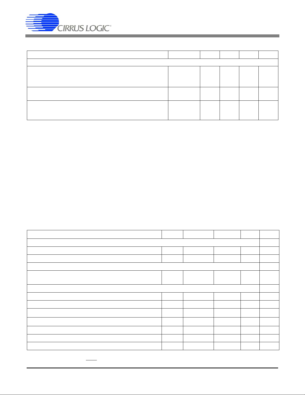
ANALOG CHARACTERISTICS (continued)
PSRR 20
106.07
V
eq
------------------
log=
Parameter Symbol Min Typ Max Unit
Power Supplies
Power Supply Currents I
Typical VA+=VD+=+3V; VA-=-2V I
Power Consumption
(Note 2) Without CPD
Power Supply Rejection (DC)
50, 60 Hz (Note 3) Voltage Channel
50, 60 Hz (Note 3) Current Channel
with CPD
D+
ID+ without CPD
With CPD
A+
PSCA
PSCD
PSCD
PC
PC
PSRR
PSRR
PSRR
50
50
60
CS5451A
-
-
-
-
-
4.0
5.0
1.0
27
23
65
90
5.3
6.3
1.5
35
31
-
-
-
mA
mA
mA
mW
mW
dB
dB
dB
Notes:
1. Specifications for Gain = 20 apply only to Current Channels. Voltage Channels are fixed to Gain = 1
2. All outputs unloaded. All inputs CMOS level.
3. Definition for PSRR: VREFIN tied to VREFOUT, VA+ = VD+ = 3 V, AGND = DGND = 0 V, VA- = -2 V (using chargepump circuit with CPD). In addition, a 106.07 mV rms (60 Hz) sinewave is imposed onto the VA+ and VD+ pins.
The “+” and “-” input pins of both input channels are shorted to VA-. 2048 instantaneous digital output data words
are collected for the channel under test. The rms value of the digital sinusoidal output signal is calculated, and this
rms value is converted into the rms value of the sinusoidal voltage (measured in mV) that would need to be applied
at the channel’s inputs, in order to cause the same digital sinusoidal output. This voltage is then defined as Veq.
PSRR is then (in dB):
DIGITAL CHARACTERISTICS (See Note 4)
• Min/Max characteristics and specifications are guaranteed over all Operating Conditions.
• Typical characteristics and specifications are measured at nominal supply voltages and TA = 25 °C.
• VA+ = VD+ = 3V ±10%; VA- = -2 V ±10%; AGND = DGND = 0 V. All voltages with respect to 0 V.
• XIN = 4.096 MHz
Parameter Symbol Min Typ Max Unit
Master Clock Characteristics
Master Clock Frequency XIN 3 4.096 5 MHz
Master Clock Duty Cycle 40 - 60 %
Filter Characteristics
High Rate Filter Output Word Rate OWRS = 0
OWRS = 1
Input/Output Characteristics
High-Level Input Voltage V
Low-Level Input Voltage V
High-Level Output Voltage I
Low-Level Output Voltage I
= -5.0 mA
out
= 5.0 mA
out
Input Leakage Current (Note 5) I
3-State Leakage Current I
Digital Output Pin Capacitance C
OWR
OWR
IH
IL
V
OH
V
OL
in
OZ
out
-
-
XIN/2048
XIN/1024
-
-
Hz
Hz
0.6 VD+ - VD+ V
0.0 - 0.8 V
(VD+) - 1.0 - - V
--0.4V
-±1±10µA
--±10µA
-9-pF
Notes: 4. All measurements performed under static conditions.
5. For OWRS and GAIN
DS635F4 5
pins, input leakage current is 30 µA (Max).
Page 6

SWITCHING CHARACTERISTICS
t
7
t
2
t
1
t
3
4
t
5
t
MSB(V1) MSB(V1) - 1 LSB(I3)
SE
6
t
SDO
SCLK
FSO
Figure 1. Serial Port Timing
• Min/Max characteristics and specifications are guaranteed over all Operating Conditions.
• Typical characteristics and specifications are measured at nominal supply voltages and TA = 25 °C.
• VA+ = VD+ = 3 V ±10%; VA- = -2 V ±10%; AGND = DGND = 0 V. All voltages with respect to 0 V.
• Logic Levels: Logic 0 = 0 V, Logic 1 = VD+
Parameter Symbol Min Typ Max Unit
Rise Times Any Digital Input (except XIN)
(Note 6) XIN only
t
rise
Any Digital Output
Fall Times Any Digital Input (except XIN)
(Note 6) XIN only
t
fall
Any Digital Output
Serial Port Timing
Serial Clock Frequency OWRS = “0”
(Note 7) OWRS = “1”
Serial Clock Pulse Width High
(Note 7 and 8) Pulse Width Low
SCLK falling to New Data Bit t
FSO Falling to SCLK Rising Delay (Note 7 & 8) t
FSO Pulse Width (Note 7 & 8) t
SE Rising to Output Enabled (Note 9) t
SE Falling to Output in Tri-state t
SCLK
SCLK
t
1
t
2
3
4
5
6
7
Notes: 6. Specified using 10% and 90% points on wave-form of interest. Output loaded with 50 pF.
7. Device parameters are specified with XIN = 4.096 MHz.
8. Device parameters are specified with OWRS = 1.
9. After SE is asserted, the states of SDO and SCLK are FSO is undefined.
-
-
-
-
-
-
-
-
-
-
-
-
50
-
-
50
500
1000
0.5
0.5
- - 50 ns
-0.5-SCLK
-1-SCLK
- - 50 ns
- - 50 ns
CS5451A
1.0
10
-
1.0
10
-
-
-
-
-
µs
ns
ns
µs
ns
ns
kHz
kHz
SCLK
SCLK
6 DS635F4
Page 7

CS5451A
ABSOLUTE MAXIMUM RATINGS
WARNING: Operation at or beyond these limits may result in permanent damage to the device.
Normal operation is not guaranteed at these extremes.
Parameter Symbol Min Typ Max Unit
DC Power Supplies Positive Digital
Positive Analog
Negative Analog
Input Current, Any Pin Except Supplies (Note 10 and 11) I
Output Current I
Power Dissipation (Note 12) PDN - - 500 mW
Analog Input Voltage All Analog Pins V
Digital Input Voltage All Digital Pins V
Ambient Operating Temperature T
Storage Temperature T
VD+
VA+
VA-
IN
OUT
INA
IND
A
stg
-0.3
-0.3
-2.5
-
-
+3.5
+3.5
-0.3
V
V
V
--±10mA
--±25mA
(VA-) - 0.3 - (VA+) + 0.3 V
-0.3 - (VD+) + 0.3 V
-40 - 85 °C
-65 - 150 °C
Notes:
10. Applies to all pins including continuous over-voltage conditions at the analog input (AIN) pins.
11. Transient current of up to 100 mA will not cause SCR latch-up. Maximum input current for a power supply pin is
±50 mA.
12. Total power dissipation, including all input currents and output currents.
DS635F4 7
Page 8

CS5451A
VA+
VD+
VIN1+, VIN2+, or VIN3+
VIN1-, VIN2-, or VIN3-
IIN1+, IIN2+, or IIN3+
IIN1-,IIN2-, or IIN3-
AGND
DGND
REFIN
REFOUT
Optional
External
Reference
V
PHASE
+
I
-2 V
PHASE
VA-
+3 V
1.2 V
NOTE: Current input channels
actually measure voltage.
Figure 2. Typical Connection Diagram
3. THEORY OF OPERATION
The CS5451A is a six-channel analog-to-digital co nverter (ADC) followed by a serial interface that allows communication with a target device. The analog inputs are
structured for 3-phase power meter applications, with
three dedicated voltage and current channels. Figure 2
illustrates the CS5451A typical inputs and power supply
connections.
The voltage-sensing element introduces a voltage
waveform on the voltage channel inputs VIN(1-3) and
is subject to a fixed 1x gain amplifier. A fourth-order delta-sigma modulator samples the amplified signal for digitization.
Simultaneously, the current-sensing element introduces
a voltage waveform on the current channel input
IIN(1-3) and is subject to two selectable gains of the
programmable gain amplifier (PGA). The amplified signal is sampled by a fourth-order delta-sigma modulator
for digitization. Both converters sample at a rate of
XIN/8, the over-sampling provides a wide dynamic
range and simplified anti-alias filter design.
The decimating digital filters on all channels are Sinc
filters. The single bit data is passed to the low-pass decimation filter and output at a fixed word rate. The decimation rate is selectable for two output word rates.
The 16-bit output word is then transmitted via a master
serial data port. The six-channel data is multiplexed on
the serial data output and is preceded by a frame sync
signal.
3
8 DS635F4
Page 9

CS5451A
800mV
P
2
-----------------
565.69mV
RMS
Hz
1z
DR–
–
1z
1–
–
----------------------
3
=
4. FUNCTIONAL DESCRIPTION
4.1 Analog Inputs
The CS5451A is equipped with six fully differential input
channels. The inputs VIN(1-3) and IIN(1-3) are designated as the voltage and current channel inputs, respectively. The full-scale differential input voltage for
the current and voltage channel is 800 mV
(gain = 1x).
4.1.1 Voltage Channel
The output of the line voltage resistive divider or transformer is connected to the VIN(1-3)+ and VIN(1- 3)- input pins of the CS5451A. The voltage channels are
equipped with a 1x fixed gain amplifie r. The full-scale
signal level that can be applied to the voltage channel is
800 mV. If the input signal is a sine wave the maximum
RMS voltage is:
which is approximately 70.7% of maximum peak voltage.
4.1.2 Current Channel
The output of the current sense resistor or transformer
is connected to the IIN(1-3)+ and IIN(1-3)- input pins of
the CS5451A. To accommodate different cu rrent-se nsing devices the current channels incorporates a programmable gain amplifier (PGA) that can be set to one
of two input ranges. Input pin GAIN
the PGA’s two gain selections and corresponding maximum input signal level.
GAIN
0 ±40mV 20x
1 ±800mV 1x
Table 1. Current Channel PGA Setting
Maximum Input Range
4.2 Digital Filters
The decimating digital filter samples the modulator bit
stream at XIN/8 and produces a fixed output word rate.
The digital filters are implemented as sinc
the following transfer function:
(see Table 1) define
3
filters with
The decimation rate is determined by the exponent DR
(see Table 2).
The output word rate (OWR) is selected by the OW RS
pin and defined by Table 2.
OWRS DR Output Word Rate
0 256 XIN/2048
P
1 128 XIN/1024
Table 2. Decimation Filter OWR
4.3 Performing Measurements
The ADC outputs are transferred in 16-bit, signed (two’s
complement) data formats. Table 3 defines the relationship between the differential voltage applied to any one
of the input channels and the corresponding output
code. Note that for the current channels, the state of the
GAIN
input pin is assumed to driven low such that the
PGA gain on the current channels is 1x. If the PGA gain
of the current channels is set to 20x, a +40 mV voltage
is applied to any pair of IIN(1- 3) pins would cause an
output code of 32767.
Differential Input
Volt age (mV)
+800 7FFF 32767
0.0122 to 0.0366 0001 1
-0.0122 to 0.0122 0000 0
-0.0122 to -0.0366 FFFF -1
-800 8000 -32768
Notes: Assume PGA gain is set to 1x.
T ab le 3. Differential Inpu t Voltage vs. Output Code
Output Code
(hexadecimal)
Output Code
(decimal)
4.4 Serial Interface
The CS5451A communicates with a target device via a
master serial data output port. Output data is provided
on the SDO output synchronous with the SCLK output.
A third output, FSO, is a framing signal used to signal
the start of output data. These three outputs will be driven as long as the SE (serial enable) input is held high.
Otherwise, these outputs will be high-impedance.
Data out (SDO) changes as a result of SCLK falling, and
always outputs valid data on the rising edge of SCLK.
When data is being transferred the SCLK frequency is
XIN/8 when OWRS is low or XIN/4 when OWRS is high.
DS635F4 9
Page 10

CS5451A
SCLK
FSO
SDO
12151413
0123456789
1011
151413 12 11 10 9 8 7654321
Channel 1 (I )
Channel 1 ( V )
01514
. . .
Ch. 2 ( V ) Ch. 2 ( I )
Ch. 3 ( V ) Ch. 3 ( I )
... ... ...
. . .
. . .
. . .
[ Low ]
[ Low ]
. . .
. . .
. . .
012
3
96 SCLKs
Figure 3. One Data Frame
SCLK
FSO
SDO
Channel 1 V
Channel 2 I
Channel 3 I
Channel 2 V
Channel 3 V
Channel 1 I
Each data segment
is 16 bits long.
96 SCLKs
Figure 4. Serial Port Data Transfer
When data is not being transferred SCLK is held low.
(see Figure 3.)
The framing signal (FSO) output is normally low. FSO
goes high, with a pulse width equal to one SCLK period,
when the instantaneous voltage and current data samples are about to be transmitted out of the serial interface (after each A/D conversion cycle). SCLK is not
active during FSO high.
For 96 SCLK periods after FSO falls, SCLK is active and
SDO provides valid output. Six channels of 16-bit data
are output, MSB first. Figure 4
illustrates how the volt-
age and current measurements are output for the three
phases. SCLK will then be held low until the next sample period.
4.5 System Initialization
A hardware reset is initiated when the RESET pin is
forced low with a minimum pulse width of 50 ns. When
RESET
is activated, all internal registers are set to a de-
fault state.
Upon powering up, the RESET
pin must be held low
(active) until after the power stabilizes.
4.6 Voltage Reference
The CS5451A is specified for operation with a +1.2 V
reference between the VREFIN and AGND pins. The
converter includes an internal 1.2 V reference that can
be used by connecting the VREFOUT pin to the VREFIN pin of the device. The VREFIN can be used to connect external filtering and/or references.
4.7 Power Supply
The low, stable analog power consumption and super ior
supply rejection of the CS5451A allow for the use of a
simple charge-pump negative supply generator. The
use of a negative supply alleviates the need for level
10 DS635F4
Page 11

shifting of the analog inputs. The CPD pin and capacitor
AGND
BAT 85
D1
C1
39 nF
C2
CPD
VA-
BAT 85
1µF
D2
Figure 5. Generating VA- with a Charge Pump
C1 provide the necessary analog supply current as
shown in Figure 5. The Schottky diodes D1 and D2 are
chosen for their low forward voltages and high-speed
capabilities. The capacitor C2 provides the required
charge storage and bypassing of the negative supply.
The CPD output signal provides the charge pump driver
signal. The frequency of the charge pump driver signal
is synchronous to XIN. The nominal average frequency
is 1 MHz. The level on the VA- pin is fed back internally
so that the CPD output will regulate the VA- level to -2/3
of VA+ level.
The value of capacitor C1 (see Figure 5) is dependent
on the XIN clock frequency. The 39 nF value for C1 was
selected for a XIN clock frequency equal to 4.096 MHz.
For more information about the operation of this type of
charge pump circuit, the reader can refer to Cirrus Logic, Inc.’s application note AN152: Using the
CS5451A
CS5521/24/28, and CS5525/26 Charge Pump Drive for
External Loads.
DS635F4 11
Page 12

CS5451A
28L SSOP PACKAGE DRAWING
E
N
1
23
e
b
2
A1
A2
A
D
SEATING
PLANE
E1
1
L
SIDE VIEW
END VIEW
TOP VIEW
5. PACKAGE DIMENSIONS
INCHES MILLIMETERS NOTE
DIM MIN NOM MAX MIN NOM MAX
A -- -- 0.084 -- -- 2.13
A1 0.002 0.006 0.010 0.05 0.13 0.25
A2 0.064 0.069 0.074 1.62 1.75 1.88
b 0.009 -- 0.015 0.22 -- 0.38 2,3
D 0.390 0.4015 0.413 9.90 10.20 10.50 1
E 0.291 0.307 0.323 7.40 7.80 8.20
E1 0.197 0.209 0.220 5.00 5.30 5.60 1
e 0.022 0.026 0.030 0.55 0.65 0.75
L 0.025 0.0354 0.041 0.63 0.90 1.03
0° 4° 8° 0° 4° 8°
JEDEC #: MO-150
Notes: 1. “D” and “E1” are reference datums and do not included mold flash or protrusions, but do include mold mismatch
and are measured at the parting line, mold flash or protrusions shall not exceed 0.20 mm per side.
2. Dimension “b” does not include dambar protrusion/intrusion. Allowable dambar protrusion shall be 0.13 mm total in
excess of “b” dimension at maximum material condition. Dambar intrusion shall not reduce dimension “b” by more
than 0.07 mm at least material condition.
3. These dimensions apply to the flat section of the lead between 0.10 and 0.25 mm from lead tips.
12 DS635F4
Page 13

CS5451A
6. ORDERING INFORMATION
Model Temperature Package
CS5451A-ISZ (lead free) -40 to +85 °C 28-pin SSOP
7. ENVIRONMENTAL, MANUFACTURING, & HANDLING INFORMATION
Model Number Peak Reflow Temp MSL Rating* Max Floor Life
CS5451A-ISZ (lead free)
* MSL (Moisture Sensitivity Level) as specified by IPC/JEDEC J-STD-020.
260 °C 3 7 Days
DS635F4 13
Page 14
8. REVISION HISTORY
Contacting Cirrus Logic Support
For all product questions and inquiries contact a Cirrus Logic Sales Representative.
To find the one nearest to you go to www.cirrus.com
IMPORTANT NOTICE
Cirrus Logic, Inc. and its subsidiaries (“Cirrus”) belie ve that the in formatio n containe d in this docu ment is accu rate and re liable. However, the information is subject
to change without not ic e and i s pr ov i ded “A S I S” wi tho ut war ra nty of any kind (express or i mpl i ed) . Cus tomer s are a dvi s ed t o o b tain the latest version of relevant
information to verify, before placing orders, that information being relied on is current and complete. All products are sold subject to the terms and conditions of sale
supplied at the time of order acknowledgment, including those pertaining to warranty, indemnification, and limitation of liability. No responsibility is assumed by
Cirrus for the use of this information, including use of this information as the basis for manufacture or sale of any items, or for infringement of patents or other rights
of third parties. This document is the property of Cirrus an d by furnishing this info rmation, Cirrus grants no lice nse, express or implied under any patents, mask work
rights, copyright s, t rad emarks , tr ade se cret s or o th er int ell ect ual property rights. Cirrus owns the copyrights associated with the information contained herein and
gives consent for copies to be made of the information only for use within your or ganization with respect to Cirrus inte grated circuits or other products of Cirrus. This
consent does not extend to other copying such as copying for general distribution, advertising or promotional purposes, or for creating any work for resale.
CERTAIN APPLICATIONS USING SEMICONDUCTOR PRODUCTS MAY INVOLVE POTENTIAL RISKS OF DEATH, PERSONAL INJURY, OR SEVERE PROPERTY OR ENVIRONMENTAL DAMAGE (“CRITICAL AP PLICATIONS”). CIRRUS PRODUCTS ARE NOT DESIGNED, AUTHORIZED OR WARRANTED FOR
USE IN PRODUCTS SURGICALLY IMPLANTED INTO THE BODY, AUTOMOTIVE SAFETY OR SECURITY DEVICES, LIFE SUPPORT PRODUCTS OR OTHER
CRITICAL APPLICATIONS. INCLUSION OF CIRRUS PRODUCTS IN SUCH APPLICATIONS IS UNDERSTOOD TO BE FULLY AT THE CUSTOMER'S RI SK
AND CIRRUS DISCLAIMS AND MAKES NO WARRANTY, EXPRESS, STATUTORY OR IMPLIED, INCLUDING THE IMPLIED WARRANTIES OF MERCHANTABILITY AND FITNESS FOR PARTICULAR PURPOSE, WITH REGARD TO ANY CIRRUS PRODUCT THAT IS USED IN SUCH A MANNER. IF THE CUSTOMER OR CUSTOMER'S CUSTOMER USES OR PERMITS THE USE OF CIRRUS PRODUCTS IN CRITICAL APPLICATIONS, CUSTOMER AGREES, BY SUCH
USE, TO FULLY INDEMNIFY CIRRUS, ITS OFFICERS, DIRECTORS, EMPLOYEES, DISTRIBUTORS AND OTHER AGENTS FROM ANY AND ALL LIABILITY,
INCLUDING ATTORNEYS' FEES AND COSTS, THAT MAY RESULT FROM OR ARISE IN CONNECTION WITH THESE USES.
Cirrus Logic, Cirrus, and the Cirrus Logic logo designs are trademarks of Cirrus Logic, Inc. All other brand and product names in this document may be trademarks
or service marks of their respective owners.
Revision Date Changes
A1 JUL 2003 Initial Release
PP1 OCT 2003 Initial release for Preliminary Product Information
F1 FEB 2005 Update electrical specifications w/ most-current characterization data.
F2 AUG 2005 Update electrical specifications w/ most-current characterization data. Added
MSL data.
F3 FEB 2010 Corrected typical input sampling rate from XIN/4 to XIN/8 (Hz).
F4 APR 2011 Removed lead-containing (Pb) device ordering information.
CS5451A
14 DS635F4
 Loading...