

Page 1
CS53L30
Digital Processing
Control
Port
Level Shifters
MIC1_BIAS
Serial Port
MIC2_BIAS
VP
MCLK
DMIC1_SCLK
MIC3_BIAS
MIC4_BIAS
–6 to +12 dB,
0.5 dB steps
+10 or +20 dB
ADC1B
–
+
–
+
Decimators
MIC1 B i a s
MIC2 B i a s
MIC3 B i a s
MIC4 B i a s
HPF , No i se
Gate, Volume,
Mute
Audio
Serial Port
Control Port
RESET
MCLK_INT
Clock Divider
Synchronizer
DMIC
ADC1A
–
+
LDO
VA
VD
2
2
4
MCLK_INT
HPF , No i se
Gate, Volume,
Mute
SYNC
MUTE
Synchronous
SRC
IN1+ /DMIC1_SD
IN2–
IN1–
IN2+
DMIC2_SCLK
–
+
–6 to +12 dB,
0.5 dB steps
+10 or +20 dB
ADC2B
–
+
–
+
Decimators
ADC2A
–
+
MCLK_INT
IN3+/DMIC2_SD
IN4–
IN3–
IN4+
–
+
CS53L30
Low-Power Quad-Channel Microphone ADC with TDM Output
Analog Input and ADC Features
91-dB dynamic range (A-weighted) @ 0-dB gain
–84-dB THD+N @ 0-dB gain
Four fully differential inputs: Four an alog mic/line inputs
Four analog programmable gain amp lifie rs
–6 to +12 dB, in 0.5-dB steps
+10 or +20 dB boost for mic input
Four mic bias generators
MUTE pin for quick mic mute and programmable quick
power down
Digital Processing Features
Volume contro l, mute, programmable high-pass filter,
noise gate
Two digital mic (DMIC) interfaces
Digital Output Features
Two DMIC SCLK generators
2
Four-channel I
can be used to output 16 channels of 24-bit 16-kHz
sample rate data on a single TDM line.
S output or TDM output. Four CS53L30s
System Features
Native (no PLL required) support for 6-/12-MHz, 6.144-/
12.288-MHz, 5.6448-/1 1.2896-MHz, or 19.2-MHz ma ster
clock rates and 8- to 48-kHz audio sample rates
Master or Slave Mode. Clock dividers can be used to
generate common audio clocks from single-master clock
input.
Low power consumption
Less than 4.5-mW stereo (16 kHz) analog mic record
Less than 2.5-mW mono (8 kHz) analog mic record
Selectable mic bias and digital interface logic voltages
High-speed (400-kHz) I²C™ control port
Available in 30-ball WLCSP and 32-pin QFN
Applications
Voice-recognition systems
Advanced headsets and telephony systems
Voice recorders
Digital cameras and video cameras
http://www.cirrus.com
Copyright Cirrus Logic, Inc. 2013
(All Rights Reserved)
DS992F1
MAY '13
Page 2

CS53L30
General Description
The CS53L30 is a high-performance, low-power, quad-channel ADC. It is designed for use in multiple-mic applications
while consuming minimal board space and po we r.
The flexible ADC inputs can accommodate four channels of analog mic or line-input data in differential, pseudodifferential,
or single-ended mode, or four channels of digital mic data. The analog input path includes a +10- to +20-dB boost and a
–6- to +12-dB PGA. Digital mic data bypasses the analog gain circuits and is fed directly to the decimators.
Four mic bias generators are integrated into the device. The device also includes two digital mic serial clock outputs.
The CS53L30 includes several digital signal processing features such as high-pass filters, noise gate, and volume control.
The device can output its four channels of audio data over two I
CS53L30s can be used to output up to 16 channels of data over a single TDM line. This is done by settin g the appropriate
frame slots for each device, and each device then alternates between outputting data and setting the output pin to high
impedance.
The CS53L30 can operate as a serial port clock master or slave. In Master Mode, clock dividers are used to generate the
internal master clock and audio clocks from either the 6-/12-MHz, 6.144-/12.288-MHz, 5.6448-/11.2896-MHz, or 19.2-MHz
master clock.
The device is powered from VA, a 1.8-V nominal supply and VP, a typical battery supply. An internal LDO on the VA supply
powers the device’s digital core. The VP supply powers the mic bias generators and the AFE.
The CS53L30 is controlled by an I
pitch WLCSP package and 32-pin 5 x 5-mm QFN package.
2
C control port. A reset pin is also included. The device is available in a 30-ball 0.4-mm
2
S ports or a single TDM port. Additionally, up to four
2 DS992F1
Page 3

Table of Contents
1.1 WLCSP . . . . . . . . . . . . . . . . . . . . . . . . . . . . . . . . . . . . . . . . . . 4
1.2 QFN . . . . . . . . . . . . . . . . . . . . . . . . . . . . . . . . . . . . . . . . . . . . 5
1.3 Pin Descriptions . . . . . . . . . . . . . . . . . . . . . . . . . . . . . . . . . . . 5
Table 3-1. Recommended Operating Conditions . . . . . . . . . . . . . . . . . . 9
Table 3-2. Absolute Maximum Ratings . . . . . . . . . . . . . . . . . . . . . . . . . . 9
Table 3-3. Combined ADC On-Chip Analog, Digital Filter, SRC, and DMIC
Characteristics . . . . . . . . . . . . . . . . . . . . . . . . . . . . . . . . . . . . . . . . . . . . . 9
Table 3-4. ADC High-Pass Filter (HPF) Characteristics . . . . . . . . . . . . . 9
Table 3-5. Analog-Input-to-Serial-Port Characteristics . . . . . . . . . . . . . 10
Table 3-6. MIC BIAS Characteristics . . . . . . . . . . . . . . . . . . . . . . . . . . 11
Table 3-7. Power-Supply Rejection Ratio (PSRR) Characteristics . . . . 11
Table 3-8. Power Consumption . . . . . . . . . . . . . . . . . . . . . . . . . . . . . . 12
Table 3-9. Switching Specifications—Digital Mic Interface . . . . . . . . . . 14
Table 3-10. Specifications—I
2
S . . . . . . . . . . . . . . . . . . . . . . . . . . . . . . 14
Table 3-11. Switching Specifications—Time-Division Multiplexed (TDM)
Mode . . . . . . . . . . . . . . . . . . . . . . . . . . . . . . . . . . . . . . . . . . . . . . . . . . . 15
Table 3-12. Switching Specifications—I
2
C Control Port . . . . . . . . . . . . 16
Table 3-13. Digital Interface Specifications and Characteristics . . . . . . 17
Table 3-14. Thermal Overload Detection Characteristics . . . . . . . . . . . 17
4.1 Overview . . . . . . . . . . . . . . . . . . . . . . . . . . . . . . . . . . . . . . . 18
4.2 Resets . . . . . . . . . . . . . . . . . . . . . . . . . . . . . . . . . . . . . . . . . 19
4.3 Interrupts . . . . . . . . . . . . . . . . . . . . . . . . . . . . . . . . . . . . . . . 19
4.4 Capture-Path Inputs . . . . . . . . . . . . . . . . . . . . . . . . . . . . . . . 20
4.5 Digital Microphone (DMIC) Interface . . . . . . . . . . . . . . . . . . 23
4.6 Serial Ports . . . . . . . . . . . . . . . . . . . . . . . . . . . . . . . . . . . . . . 25
4.7 TDM Mode . . . . . . . . . . . . . . . . . . . . . . . . . . . . . . . . . . . . . . 29
4.8 Synchronous Sample-Rate Converter (SRC) . . . . . . . . . . . .33
4.9 Multichip Synchronization Protocol . . . . . . . . . . . . . . . . . . . 34
4.10 Input Path Source Selection and Poweri ng . . . . . . . . . . . .34
4.11 Thermal Overload Notification . . . . . . . . . . . . . . . . . . . . . . 34
4.12 MUTE Pin . . . . . . . . . . . . . . . . . . . . . . . . . . . . . . . . . . . . . . 35
4.13 Power-Up and Power-Down Control . . . . . . . . . . . . . . . . . 35
4.14 I
2
C Control Port . . . . . . . . . . . . . . . . . . . . . . . . . . . . . . . . . 35
4.15 QFN Thermal Pad . . . . . . . . . . . . . . . . . . . . . . . . . . . . . . . 37
5.1 Octal Microphone Array to the Audio Serial Port . . . . . . . . . 38
5.2 Power-Up Sequence . . . . . . . . . . . . . . . . . . . . . . . . . . . . . .39
5.3 Power-Down Sequence . . . . . . . . . . . . . . . . . . . . . . . . . . . . 41
5.4 Capture-Path Inputs . . . . . . . . . . . . . . . . . . . . . . . . . . . . . . . 42
5.5 MCLK Jitter . . . . . . . . . . . . . . . . . . . . . . . . . . . . . . . . . . . . . . 44
5.6 Frequency Response Considerations . . . . . . . . . . . . . . . . . 44
5.7 Connecting Unused Pins . . . . . . . . . . . . . . . . . . . . . . . . . . . 44
7 Register Descriptions . . . . . . . . . . . . . . . . . . . . . . . . . . . . . . . . 47
7.1 Device ID A and B . . . . . . . . . . . . . . . . . . . . . . . . . . . . . . . . 47
7.2 Device ID C and D . . . . . . . . . . . . . . . . . . . . . . . . . . . . . . . . 47
7.3 Device ID E . . . . . . . . . . . . . . . . . . . . . . . . . . . . . . . . . . . . . 47
7.4 Revision ID . . . . . . . . . . . . . . . . . . . . . . . . . . . . . . . . . . . . . . 47
7.5 Power Control . . . . . . . . . . . . . . . . . . . . . . . . . . . . . . . . . . . . 47
7.6 MCLK Control . . . . . . . . . . . . . . . . . . . . . . . . . . . . . . . . . . . . 48
7.7 Internal Sample Rate Control . . . . . . . . . . . . . . . . . . . . . . . . 48
7.8 Mic Bias Control . . . . . . . . . . . . . . . . . . . . . . . . . . . . . . . . . . 49
7.9 ASP Configuration Control . . . . . . . . . . . . . . . . . . . . . . . . . . 49
7.10 ASP Control 1 . . . . . . . . . . . . . . . . . . . . . . . . . . . . . . . . . . . 49
7.11 ASP TDM TX Control 1–4 . . . . . . . . . . . . . . . . . . . . . . . . .50
7.12 ASP TDM TX Enable 1–6 . . . . . . . . . . . . . . . . . . . . . . . . . . 50
7.13 ASP Control 2 . . . . . . . . . . . . . . . . . . . . . . . . . . . . . . . . . . . 50
7.14 Soft Ramp Control . . . . . . . . . . . . . . . . . . . . . . . . . . . . . . . 50
7.15 LRCK Control 1 . . . . . . . . . . . . . . . . . . . . . . . . . . . . . . . . . 51
7.16 LRCK Control 2 . . . . . . . . . . . . . . . . . . . . . . . . . . . . . . . . . 51
7.17 MUTE
Pin Control 1 . . . . . . . . . . . . . . . . . . . . . . . . . . . . . . 51
7.18 MUTE Pin Control 2 . . . . . . . . . . . . . . . . . . . . . . . . . . . . . . 51
7.19 Input Bias Control 1 . . . . . . . . . . . . . . . . . . . . . . . . . . . . . . 52
7.20 Input Bias Control 2 . . . . . . . . . . . . . . . . . . . . . . . . . . . . . . 52
7.21 DMIC1 Stereo Control . . . . . . . . . . . . . . . . . . . . . . . . . . . . 52
7.22 DMIC2 Stereo Control . . . . . . . . . . . . . . . . . . . . . . . . . . . . 52
7.23 ADC1/DMIC1 Control 1 . . . . . . . . . . . . . . . . . . . . . . . . . . . 52
7.24 ADC1/DMIC1 Control 2 . . . . . . . . . . . . . . . . . . . . . . . . . . . 53
7.25 ADC1 Control 3 . . . . . . . . . . . . . . . . . . . . . . . . . . . . . . . . . 53
7.26 ADC1 Noise Gate Control . . . . . . . . . . . . . . . . . . . . . . . . . 54
7.27 ADC1A/1B AFE Control . . . . . . . . . . . . . . . . . . . . . . . . . . . 54
7.28 ADC1A/1B Digital Volume . . . . . . . . . . . . . . . . . . . . . . . . . 54
7.29 ADC2/DMIC2 Control 1 . . . . . . . . . . . . . . . . . . . . . . . . . . . 55
7.30 ADC2/DMIC2 Control 2 . . . . . . . . . . . . . . . . . . . . . . . . . . . 55
7.31 ADC2 Control 3 . . . . . . . . . . . . . . . . . . . . . . . . . . . . . . . . . 55
7.32 ADC2 Noise Gate Control . . . . . . . . . . . . . . . . . . . . . . . . . 56
7.33 ADC2A/2B AFE Control . . . . . . . . . . . . . . . . . . . . . . . . . . . 56
7.34 ADC2A/2B Digital Volume . . . . . . . . . . . . . . . . . . . . . . . . . 56
7.35 Device Interrupt Mask . . . . . . . . . . . . . . . . . . . . . . . . . . . . 57
7.36 Device Interrupt Status . . . . . . . . . . . . . . . . . . . . . . . . . . . . 57
8 Parameter Definitions . . . . . . . . . . . . . . . . . . . . . . . . . . . . . . . . 58
9 Plots . . . . . . . . . . . . . . . . . . . . . . . . . . . . . . . . . . . . . . . . . . . . . . 58
9.1 Digital Filter Response . . . . . . . . . . . . . . . . . . . . . . . . . . . . . 58
9.2 PGA Gain Linearity . . . . . . . . . . . . . . . . . . . . . . . . . . . . . . . .62
9.3 Dynamic Range Versus Sampling Frequency . . . . . . . . . . .63
9.4 FFTs . . . . . . . . . . . . . . . . . . . . . . . . . . . . . . . . . . . . . . . . . . . 63
10 Package Dimensions . . . . . . . . . . . . . . . . . . . . . . . . . . . . . . . . 65
10.1 WLCSP Package . . . . . . . . . . . . . . . . . . . . . . . . . . . . . . . . 65
10.2 QFN Package . . . . . . . . . . . . . . . . . . . . . . . . . . . . . . . . . . . 66
11 Thermal Characteristics . . . . . . . . . . . . . . . . . . . . . . . . . . . . . 66
12 Ordering Information . . . . . . . . . . . . . . . . . . . . . . . . . . . . . . . . 66
13 Revision History . . . . . . . . . . . . . . . . . . . . . . . . . . . . . . . . . . . . 67
CS53L30
DS992F1 3
Page 4
1 Pin Descriptions
A1A2A3A4A5A6B1
B2
B3B4B5B6C1C2C3C4C5
C6
D1D2D3D4D5
D6
E1E2E3E4E5
E6
Filter pins Analog outputs Digital I/O
PowerCapture-path pins
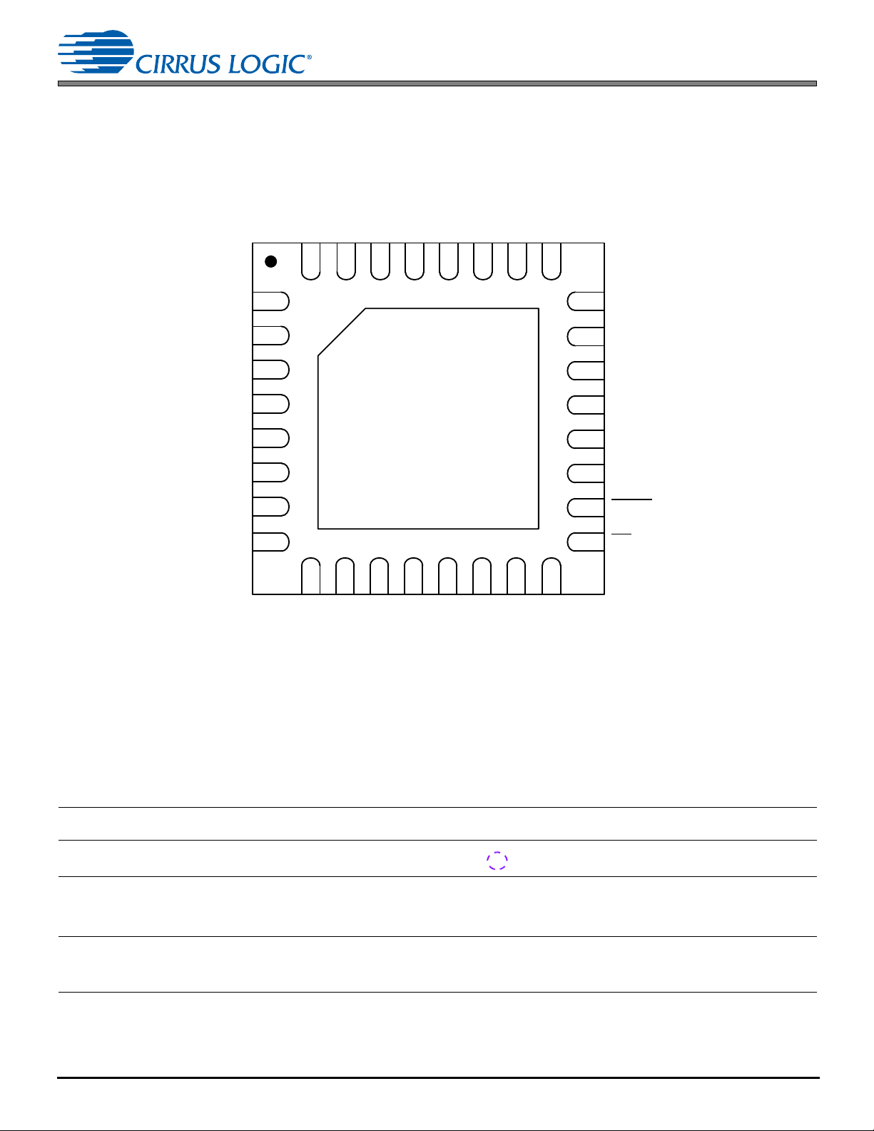
1.1 WLCSP
CS53L30
1 Pin Descriptions
IN1+/DMIC1_
SD
IN1– IN2– IN3– IN4– GNDA VP
DMIC2_SCLK/
AD1
ASP_SDOUT1 ASP_SCLK SCL SYNC MIC4_BIAS MIC_BIAS_
MCLK SDA ASP_SDOUT2/
IN2+ IN3+/DMIC2_
SD
DMIC1_SCLK ASP_LRCK/
FSYNC
AD0
IN4+ VA FILT+
MIC1_BIAS MIC2_BIAS MIC3_BIAS
FILT
GNDD RESET
MUTE
Figure 1-1. Top-Down (Through-Package) View—30-Ball WLCSP Package
4 DS992F1
Page 5
1.2 QFN
Thermal Pad
109
8
7
6
5
4
3
2
1
11 12 13 14 15 16
17
18
19
20
21
22
23
24
25
262728
29
303132
SCL
ASP_SDOUT2/AD0
ASP_LRCK/FSYNC
VA
GNDD
SYNC
RESET
INTGNDA
MUTE
IN1–
DMIC2_SCLK/AD1
IN1+/DMIC1_SD
DMIC1_SCLK
ASP_SDOUT1
ASP_SCLK
MCLK
SDA
MIC_BIAS_FILT
MIC4_BIAS
MIC3_BIAS
MIC2_BIAS
MIC1_BIAS
VP
FILT+
VA
IN4–
IN4+
IN3–
IN3+/DMIC2_SD
IN2–
IN2+
Capture-Path Pins
CS53L30
1.2 QFN
1.3 Pin Descriptions
Name
IN1+/DMIC1_SD
IN2+
IN3+/DMIC2_SD
IN4+
IN1–
IN2–
IN3–
IN4–
DS992F1 5
Figure 1-2. Top-Down (Through-Package) View—32-Pin QFN Package
Ball#Pin#Power
A1
31
A2
A3
A4
B1
B2
B3
B4
1
3
5
32
2
4
6
Supply
I/O Description
VA I Noninverting Inputs/DMIC Inputs.
VA I Inverting Inputs. Negative analog inputs
Positive analog inputs for the stereo
ADCs when CH_TYPE = 0 (default) or
DMIC inputs when CH_TYPE = 1.
for the stereo ADCs when CH_TYPE = 0
(default) or unused when CH_TYPE = 1.
Table 1-1. Pin Descriptions
Internal
Connection
Programmable — Hysteresis
Programmable — Hysteresis
Driver Receiver
State at
Reset
—
on CMOS
input
—
on CMOS
input
Page 6
Table 1-1. Pin Descriptions (Cont.)
Filter pins
Analog Outputs
Digital I/O
CS53L30
1.3 Pin Descriptions
Name
MIC_BIAS_FILT D6 15 VP I Mi crophone Bias Voltage Filter. Filter
FILT+ A6 9 VA O Positive Reference Filter. Positive
MIC1_BIAS
MIC2_BIAS
MIC3_BIAS
MIC4_BIAS
INT
RESET
SYNC D4 19 VA I/O Multidevice Synchronization Signal.
SCL D3 24 VA I Serial Control Port Clock. Serial clock
SDA E2 25 VA I/O Serial Control Data. Bidirectional data
MCLK E1 26 VA I Master Clock. Clock source for device’s
ASP_SCLK D2 27 VA I/O Audio Serial Clock. Audio bit clock. Input
ASP_LRCK/
FSYNC
ASP_SDOUT1 D1 28 VA O Audio Data Output. Output for the two’s
ASP_SDOUT2/
AD0
DMIC1_SCLK C2 29 VA O Digital MIC Interface 1 Serial Clock.
Ball#Pin#Power
C4
C5
C6
D5
—17 VA OInterrupt. Outgoing interrupt signal
E5 18 VA I Reset. The device enters a low power
C3 22 VA I/O Audio Left/Right Clock/Frame SYNC.
E3 23 VA I/O Au dio Data Output/Address Select.
Supply
11
12
13
14
I/O Description
connection for the internal quiescent
voltage used for the MICx_BIAS outputs.
reference voltage filter for internal
sampling circuits.
VP O Microphone Bias Voltage. Low-noise
bias supply for an external mic.
generated upon registering an error
(fault).
mode when this pin is driven low.
Synchronization output when SYNC_EN
is set, otherwise it is a synchronization
input. Defaults to input.
2
for the I
pin for the I
core.
in Slave Mode, output in Master Mode.
Identifies the start of each seri alized PCM
data word and indicates the active
channel on each serial PCM audio data
line. Input in Slave Mode, output in Master
Mode.
complement serial PCM data. Channels 1
and 2 are output in I
channels of data are output on this single
pin in TDM Mode.
Output for the two’s-complement serial
PCM data. Channels 3 and 4 are output in
2
I
immediately sets the I
RESET
High speed clock output to the digital
mics.
C port.
2
C port.
2
S Mode, while all four
S Mode. Along with DMIC2_SCLK/AD1,
is deasserted. Default is 0.
2
C address when
Internal
Connection
————
————
———Hi-Z
—CMOS
— — Hysteresis
Weak
pulldown
— — Hysteresis
—CMOS
Weak
pulldown
Weak
pulldown
Weak
pulldown
Weak
pulldown
Weak
pulldown
Weak
pulldown
Driver Receiver
open-drain
output
on CMOS
CMOS
output
open-drain
output
— Hysteresis
CMOS
output
CMOS
output
Tristateable
CMOS
output
Tristateable
CMOS
output
CMOS
output
Hysteresis
on CMOS
on CMOS
Hysteresis
on CMOS
on CMOS
Hysteresis
on CMOS
Hysteresis
on CMOS
—Hi-Z
input
input
input
input
input
input
input
—Hi-Z
—Hi-Z
—Hi-Z
State at
Reset
—
Hi-Z
—
—
—
Hi-Z
Hi-Z
6 DS992F1
Page 7
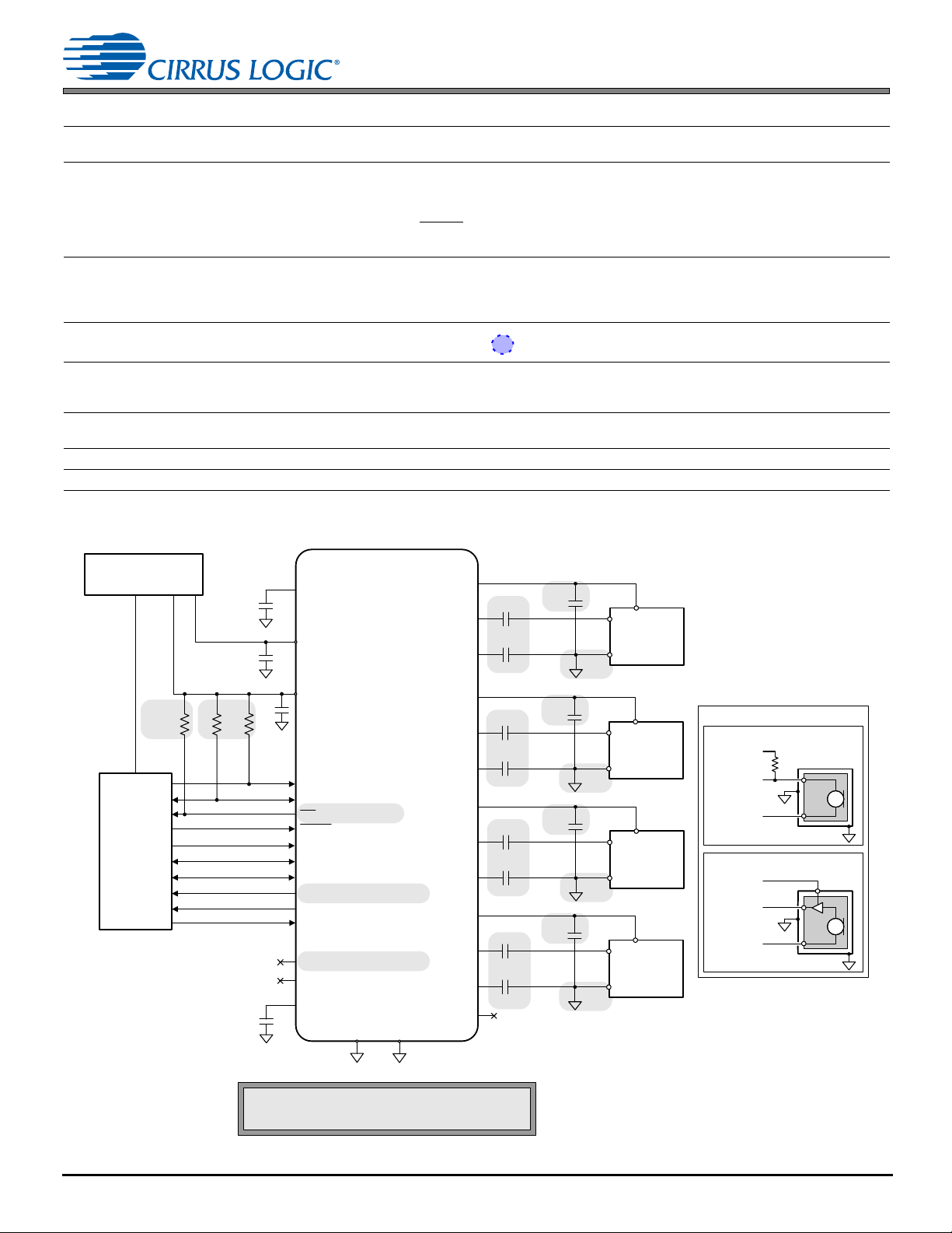
Table 1-1. Pin Descriptions (Cont.)
Power
CS53L30
GNDD
GNDA
DMIC1_SCLK
MIC1_BIAS
IN1
–
IN1+
MIC2_BIAS
IN2
–
IN2+
MIC3_BIAS
IN3
–
IN3+
MIC4_BIAS
IN4
–
IN4+
Analog Mic r op hone Conn ec tion
Two-wire microphone connection
Rbias
Ground Ring
MICx_BIAS
INx+
INx–
Three-wire microphone connection
Ground Ring
MICx_BIAS
INx+
INx–
1 µF
C
INM
C
INM
Analog
Microphone
(see
connection
diagram)
1 µF
C
INM
C
INM
Analog
Microphone
(see
connection
diagram)
1 µF
C
INM
C
INM
Analog
Microphone
(see
connection
diagram)
1 µF
C
INM
C
INM
Analog
Microphone
(see
connection
diagram)
MIC_BIAS_FILT
*
4.7 µF
SYNC
SCL
SDA
SoC
VA
0.1 µF
R
P
*
R
P
+1.8 V +1.8 V
VP
0.1 µF
*
+3.6 V
FILT+
2.2 µF
*
PMU
ASP_LRCK/F SYNC
ASP_SCLK
ASP_SDOUT2/AD0
ASP_SDOUT1
MCLK
RESET
MUTE
R
P_I
Key for Capacitor Types Required:
* U s e low ESR, X7R /X5R c apac it ors
All External Passive Component Values Shown Are Nominal Values.
DMIC2_SCLK/AD1
INT
Note 1
Note 3
Note 1
Note 3
Note 2
Note 2
Note 5
Note 4 Note 4
Note 7
Note 7
Note 2
Note 1
Note 3
Note 2
Note 1
Note 3
Note 6
CS53L30
2 Typical Connection Diagram
Name
DMIC2_SCLK/
AD1
Ball#Pin#Power
Supply
I/O Description
C1 30 VA I/O Digital MIC Interface 2 Serial Clock/
Address Select. High speed clock output
to the digital mics. Along with ASP_
SDOUT2/AD0, immediately sets the I
address when RESET
is deasserted.
2
C
Internal
Connection
Weak
pulldown
Driver Receiver
CMOS
—Hi-Z
output
State at
Reset
Default is 0.
MUTE E6 16 VA I Mute. Asserting this pin mutes all four
channels. Also can be programmed to
power down modules as configured in the
Weak
pulldown
— Hysteresis
on CMOS
input
MUTE pin control registers.
VA A5 7
N/A I Analog/Digital Power. Power supply for
21
analog circuitry and digital circuitry via
————
internal LDO.
VP B6 10 N/A I Analog Power. Power supply for mic
————
bias.
GNDA B5 8 N/A I Analog Ground. Ground reference. — — — —
GNDD E4 20 N/A I Digital Ground. Ground reference. — — — —
2 Typical Connection Diagram
—
Figure 2-1. Typical Connection Diagram—Analog Microphone Connections
DS992F1 7
Page 8
CS53L30
CS53L30
GNDDGNDA
Left Digital
Mic rophone 1
Right D igital
Mic rophone 1
IN1+/DMIC1_SD
DMIC1_SCLK
L/R
DATA
L/R
DATA
IN3+/DMIC2_SD
Left Digital
Mic rophone 2
Right Digital
Mic rophone 2
L/R
DATA
L/R
DATA
+1.8 V +1.8 V
VP
0.1 µF
*
+3.6 V
FILT+
MIC_BIAS_FILT
*
4.7 µF
PMU
SCL
SDA
SoC
VA
0.1 µ F
R
P
*
R
P
ASP_LRCK/FSYNC
ASP_SCLK
ASP_SDOUT1
MCLK
RESET
MUTE
R
P_I
Key for Capacitor Types Required:
* U s e low ESR, X7R/X5 R c apac it ors
All External Passive Component Values Shown Are Nominal Values.
0.47 µF
0. 47 µ F
0.47 µF
0.47 µF
MIC1_BIAS
MIC3_BIAS
DMIC2_SCLK/AD1
SYNC
IN1–, IN2+, IN2–,
IN3
–
, IN4+, IN4
–
ASP_SDOUT2/AD0
INT
Note 4 Note 4
Note 8
Note 7
Note 7
Note 6
2 Typical Connection Diagram
1. The MICx_BIAS compensation capacitor must be 1 µF (nominal values indicated, can vary from the nominal by ±20%). This value is bounded
by the stability of the amplifier and the maximum rise-t ime specification of the output.
Figure 2-2. Typical Connection Diagram—Digital Microphone Connections
2. The DC-blocking capacitor, C
impedance. See Table 3-5 and Section 4.4.2.
3. The reference terminal of the INx inputs connects to the ground pin of the mic cartridge in the pseudodifferential case. I n a fully differential
configuration, the reference terminal of the INx inputs connects to the inverting output terminal of differential mic.
4. R
and RP can be calculated by using the values in Table 3-14.
P_I
5. The value of R
6. The INT
7. ASP_SDOUT2/AD0 and DMIC2_SCLK/AD1 have internal pull-downs that allow for the default I
See Table 3-14 for typical and maximum pull-down values. If an I
pin is provided only on the QFN package.
, the bias resistor for electret condenser mics, is dictated by the mic cartridge.
BIAS
termination to VA is required. The minimum value resistor allowed on these I/O pins is 10 kThe time constant resulting from the pull-up/
pull-down resistor and the total net cap acit ance should be consi dered when determining the time required for the p in voltage t o settle befo re
RESET is deasserted.
8. Unconnected INx pins can be terminated with an internal weak_vcm or weak pull-down by setting the termin ation in the INxy_BIAS bit s. See
Section 5.7, Section 7.19, and Section 7.20.
, forms a high-pass filter whose corner frequency is determined by the capacitor value and the input
INM
2
C physical address other than the default is desired, then external resi stor
2
C address with no external components.
8 DS992F1
Page 9
CS53L30
3 Characteristics and Specification s
3 Characteristics and Specifications
Section 8 provides additional details about parameter definitions.
Table 3-1. Recommended Operating Conditions
Test conditions: GNDA = GNDD = 0 V; all voltages are with respect to ground.
Parameters
DC power supply Analog/Digital VA 1.71 1.89 V
External voltage applied to pin
2
Ambient temperature Commercial T
1.Device functional operation is guaranteed within these limits; operation outside them is not guaranteed or implied and may reduce device reliability.
2.The maximum over/under voltage is limited by the input current.
Table 3-2. Absolute Maximum Ratings
Test conditions: GNDA = GNDD = 0 V; all voltages are with respect to ground.
Parameters Symbol Min Max Units
DC power supply Analog/digital
Input current
Ambient operating temperature (power applied) T
Storage temperature (no power applied) T
CAUTION: Operation at or beyond these limits may permanently damage the device.
1.Any pin except supplies. Transient currents of up to ±100 mA on the capture-path pins do not cause SCR latch-up.
1
1
VP_MIN = 1
VP_MIN = 0
VA domain pins V
VP domain pins V
Mic bias
Symbol Min Max Unit
VP 3.2
3.0
IN-AI
IN-PI
A
VA
VP
I
in
A
stg
–0.3 VA + 0.3 V
–0.3 VP + 0.3 V
–10 +70 C
–0.3
–0.3
—±10mA
–50 +115 °C
–65 +150 °C
5.25
5.25
2.22
5.6
V
V
V
V
Table 3-3. Combined ADC On-Chip Analog, Digital Filter, SRC, and DMIC Characteristics
Test conditions (unless otherwise specified): TA = +25°C; MCLK = 12.288 MHz; characteristics do not include the effects of external AC-coupling
capacitors. Path is INx to SDOUT. Analog and digital gains are all set to 0 dB; HPF disabled.
1
–3.0-dB corner——
Min Typ Max Units
0.391
0.410
—
—
Fs
= Fs
int
Fs = 48 kHz
ext
=
ADC notch filter on
[2]
(ADCx_NOTCH_
DIS = 0)
Parameters
Passband –0.05-dB corner
Passband ripple (0 Hz to 0.394 Fs; normalized to 0 Hz) –0.13 — 0.14 dB
Stopband @ –70 dB — 0.492 —
ADC notch filter off
(ADCx_NOTCH_
DIS = 1)
Total group delay — 15.3/Fs
Passband –0.05-dB corner
–3.0-dB corner——
Passband ripple (0 Hz to 0.447 Fs; normalized to 0 Hz) –0.09 — 0.14 dB
+6.5/Fs
int
0.445
0.470
—s
ext
—
—
Stopband @ –70 dB — 0.639 —
Total group delay — 15.5/Fs
1.Specifications are normalized to Fs and can be denormalized by multiplying by Fs.
2.See Section 5.6 for information about combined filter response when Fs
is not equal to Fs
int
ext
.
+6.6/Fs
int
—s
ext
Table 3-4. ADC High-Pass Filter (HPF) Characteristics
Test conditions (unless specified otherwise): Analog and digital gains are all set to 0 dB; ADCx_HPF_CF = 00.
Passband
Passband ripple (0.417x10
Phase deviation @ 0.453 x 10
Filter settling time
2
–3
Fs to 0.417 Fs; normalized to 0.417 Fs) — — 0.01 dB
–3
3
Fs — 4.896 — °
ADCx_HPF_CF = 00 (3.88 x 10
ADCx_HPF_CF = 01 (2.5 x 10
ADCx_HPF_CF = 10 (4.9 x 10
ADCx_HPF_CF = 11 (9.7 x 10
Parameters
1.Response scales with Fs
2.Characteristics do not include effects of the analog HPF filter formed by the external AC-coupling capacitors and the input impedance.
3.Required time for the magnitude of the DC component present at the output of the HPF to reach 5% of the applied DC signal.
. Specifications are normalized to Fs
int
1
–0.05-dB corner
–3.0-dB corner
–5
x Fs
mode)
int
–3
x Fs
mode)
int
–3
x Fs
mode)
int
–3
x Fs
mode)
int
and are denormalized by multiplying by Fs
int
Min Typ Max Units
200/Fs
100/Fs
50/Fs
.
int
–4
–5
int
int
int
int
—
—
—
—
—
—
Fs
Fs
—
—
—
—
—
—
3.57x10
3.88x10
12260/Fs
Fs
Fs
Fs
Fs
Fs
Fs
int
int
s
s
s
s
DS992F1 9
Page 10
CS53L30
–60 dB,
1 kHz
INx+
INx–
MICx_BIAS
2.21 k
2.21 k
0.1 µF
0.1 µF
100 mVPP, 25 Hz
0.1 µF
INx+
INx–
3 Characteristics and Specification s
Table 3-5. Analog-Input-to-Serial-Port Characteristics
Test conditions (unless oth erwise spe cified): Fig. 2-1 shows CS53L30 connections; input is a full-scale 1- kHz sine wav e; ADCx_P REAMP = + 10 dB; ADCx_PGA_
VOL = 0 dB; GNDA = GNDD = 0; voltages are
min/max performance data ta ken with
Dynamic range
2
Preamp setting: Bypass, PGA setting: 0 dB A-weighted
Preamp setting: Bypass, PGA setting: +12 dB A-weighted
Preamp setting: +10 dB, PGA setting: 0 dB A-weighted
Preamp setting: +10 dB, PGA setting: +12 dB A-weighted
Preamp setting: +20 dB, PGA setting: 0 dB A-weighted
Preamp setting: +20 dB, PGA setting: +12 dB A-weighted
Total harmonic
distortion + noise
Preamp setting: Bypass, PGA setting: 0 dB –1 dB — –84 –78 dB
3
Preamp setting: Bypass, PGA setting: +12 dB –1 dB — –80 –74 dB
Preamp setting: +10 dB, PGA setting: 0 dB –1 dB — –76 –70 dB
Preamp setting: +10 dB, PGA setting: +12 dB –1 dB — –63 –57 dB
Preamp setting: +20 dB, PGA setting: 0 dB –1 dB — –70 –64 dB
Preamp setting: +20 dB, PGA setting: +12 dB –1 dB — –62 –56 dB
Common-mode rejection
4
DC accuracy Interchannel gain mismatch
Gain drift
5
— ±100 — ppm/°C
PGA A/B gain G
Preamp A/B gain G
Offset error
Phase accuracy Multichip interchannel phase mismatch
Interchannel phase mismatch
Input Interchannel isolation
Full-scale signal
input voltage
Input impedance
DC voltage at INx
(pin floating)
Preamp setting: Bypass ADCx_PDN = 0
11,12
Preamp setting: +10 dB or +20 dB ADCx_PDN = 0
1.Measures are referred to the applicable typical full-scale voltages. Applies to all THD+N and dynamic range values in the table.
2.INx dynamic range test configuration (pseudodifferential) Includes noise from MICx_BIAS
output (2.7-V setting) through a series 2.21-k resistor connected to INx. Input signal is –60 dB
down from the corresponding full-scale signal input voltage.
with respect to ground; param ete rs can vary with VA , typica l perfo rm ance data ta ken w ith VA= 1.8 V, VP = 3.6 V,
V
A = 1.8 V, VP = 3.6 V; TA = +25°C; measurement bandwidth is 20 Hz –20 kH z; LRC K= Fs = 48 kHz.
Parameters
1
unweighted8785
unweighted8078
unweighted8482
unweighted7472
unweighted7876
unweighted6664
Min Typ Max Units
93
91
86
84
90
88
80
78
84
82
72
70
—
—
—
—
—
—
—
—
—
—
—
—
—70—dB
5
MIN
G
MAX
G
MIN
G
6
7
8
8
9
10
Preamp setting: 0 dB, PGA setting: 0 dB
Preamp setting: +10 dB, PGA setting: 0 dB
Preamp setting: +10 dB, PGA setting: +12 dB
Preamp setting: +20 dB, PGA setting: 0 dB
Preamp setting: +20 dB, PGA setting: +12 dB
Preamp setting: 0 dB
MAX
217 Hz
1kHz
20 kHz
Preamp setting: +10 or +20 dB;450.9
ADCx_PDN = 1——
ADCx_PDN = 1——
—±0.2— dB
–6.25
11.75
0.375
9.5
19.9
—
—
—
—
—
—
0.78•VA
—
—
—
—
–6
12
0.5
10
20
128
0.5
0.5
90
90
80
0.82•VA
0.258•VA
0.064•VA
0.081•VA
0.020•VA
50
1
0.42•VA
0.50•VA
0.39•VA
0.50•VA
–5.75
12.25
0.625
10.5
20.5
—LSB
—
—
—
—
—
0.88•VA
—
—
—
—
—
—
—
—
—
—
dB
dB
dB
dB
dB
dB
dB
dB
dB
dB
dB
dB
dB
dB
dB
dB
dB
°
°
dB
dB
dB
Vpp
Vpp
Vpp
Vpp
Vpp
k
M
V
V
V
V
3.Input signal amplitude is relative to typical full-scale signal input voltage.
4.INx CMRR test configuration
5.Measurements taken at all defined full-scale signal input voltages.
6.SDOUT code with ADC_HPF_ EN = 1, DIG_BOOSTx = 0. The offset is added at the ADC output; if two ADC sources are mixed, their offsets add.
7.Measured between two CS53L30 chips with input pairs IN1 selected and driven from same source with an MCLK of 19.2 MHz, 16-kHz sample rate,
and 8-kHz full-scale sine wave with preamp gain of +20 dB and PGA gain of +12 dB.
8.Measured between input pairs (IN1 to INx, IN2 to INx, IN3 to INx, IN4 to INx) with +20 dB preamp gain and +12 dB PGA gain.
9.ADC full-scale input voltage is measured between INx+ and INx– with the preamp set to bypass and the PGA set to 0-dB gain. Maximum input signal
level for INx depends on the preamp and PGA gain settings described in Section 5.4.1. The digital output level corresponding to ADC full-scale input
is less than 0 dBFS due to signal attenuation through the SRC; see Table 4-4.
10.Measured between INx+ and INx–.
11.INx pins are biased as specified when weak VCM is selected in the input bias control registers; see Section 7.19 and Section 7.20.
12.Changing gain settings to Bypass Mode may cause audible artifacts due to the difference in DC operating points between modes.
10 DS992F1
Page 11
CS53L30
Operational
Amplifier
OUT
GND
Power DAC
OUT
GND
PWR
DUT
+5V +5V
++––
+
–
OUT
Analog Generator Analog Analy zer
Analog Test Equipment
Analog Output P S RR
Operational
Amplifier
OUT
GND
Power DAC
SDOUT
GND
PWR
DUT
+5V +5V
+–
+
–
OUT
Analog Generator Analog Analyzer
Test Equipment
Digital Output PSRR
Digital Analyzer
3 Characteristics and Specification s
Table 3-6. MIC BIAS Characteristics
Test conditions (unless otherwise specified): Fig. 2-1 shows CS53L30 connections; GNDA = GNDD = 0; all voltages are with respect to ground; VA =
1.8 V, VP = 3.6 V, T
Output voltage
Mic bias startup delay
Rise time
3
DC output current (I
Integrated output noise f = 100 Hz–20 kHz — 3 — µVrms
Dropout voltage
PSRR reduction voltage
Output resistance (R
1.The output voltage includes attenuation due to the MIC BIAS output resistance (R
2.Startup delay times are approximate and vary with MCLK
scaling factor. The MCLK
3.From 10% to 90% of typical output voltage. External capacitor on MICx_BIAS is as shown in Fig. 2-1.
4.Dropout voltage indicates the point where an output’s voltage starts to vary significantly with reductions to its supply voltage. When the VP supply
voltage drops below the programmed MICx_BIAS output voltage plus the dropout voltage, the MICx_BIAS output voltage progressively decreases as
its supply decreases.
Dropout voltage is measured by reducing the VP supply until MICx_BIAS drops 10 mV from its initial voltage with the default typical test condition VP
voltage (= 3.6 V, as in test conditions listed above). The difference between the VP supply voltage and the MICx_BIAS voltage at this point is the
dropout voltage. For instance, if the initial MICx_BIAS output is 2.86 V when VP = 3.6 V and VP = 3.19 V when MICx_BIAS drops to 2.85 V (–10 mV),
the dropout voltage is 340 mV (3.19 V – 2.85 V).
5.PSRR voltage indicates the point where an output’s supply PSRR starts to degrade significantly with supply voltage reductions. When the VP supply
voltage drops below the programmed MICx_BIAS output voltage plus the PSRR reduction voltage, the MICx_BIAS output’s PSRR progressively
decreases as its supply decreases.
PSRR reduction voltage is measured by reducing the VP supply until MICx_BIAS PSRR @ 217 Hz falls below 100 dB. The difference between the
VP supply voltage and the MICx_BIAS voltage at this point is the PSRR reduction voltage. For instance, if the MICx_BIAS PSRR falls to 99.9 dB
when VP is reduced to 3.25 V and the MICx_BIAS output voltage is 2.75 V at that point, PSRR reduction voltage is 500 mV (3.25 V – 2.75 V).
= +25°C; only one bias output is powered up at a time; MCLK_INT_SCALE = 0.
A
Parameters Min Typ Max Units
1
MIC_BIAS_CTRL = 01 (1.8-V mode)
MIC_BIAS_CTRL = 10 (2.7-V mode)
2
I
= 500 µA, MIC_BIAS_CTRL = 01 (1.8-V mode)
OUT
= 500 µA, MIC_BIAS_CTRL = 10 (2.7-V mode)
I
OUT
) Per output — — 2 mA
OUT
4
5
) I
OUT
frequency. If MCLK_INT_SCALE = 1, the startup delay time is scaled up by the MCLK
scaling factor is 1, 2, or 4, depending on Fs
INT
INT
EXT
= 2 mA
I
OUT
= 2-mA — 30 —
OUT
).
OUT
. See Table 4-2.
1.71
2.61
1.80
2.75
1.89
2.86
V
V
—10—ms
—
—
—
0.2
0.5
—
—
—
ms
ms
3
ms
— — 340 mV
— — 500 mV
INT
Table 3-7. Power-Supply Rejection Ratio (PSRR) Characteristics
Test conditions (unless specified otherwise): Fig. 2-1 shows CS53L30 connections; input test signal held low (all zero data); GNDA = GNDD = 0; voltages
are with respect to ground; VA = 1.8 V, VP = 3.6V; T
INx (32-dB analog gain)
PSRR with 100-mVpp signal AC coupled to VA supply
MICx_BIAS (MICx_BIAS = 2.7-V mode, I
PSRR with 100 mVpp signal AC coupled to VA supply
VP_MIN = 0 (3.0 V)
MICx_BIAS (MICx_BIAS = 2.7-V mode, I
PSRR with 100 mVpp signal AC coupled to VA supply
VP_MIN = 1 (3.2 V)
MICx_BIAS (MICx_BIAS = 2.7-V mode, I
PSRR with 100 mVpp signal AC coupled to VP supply
VP_MIN = 0 (3.0 V)
MICx_BIAS (MICx_BIAS = 2.7-V mode, I
PSRR with 1 Vpp signal AC coupled to VP supply
VP_MIN = 1 (3.2 V)
1.PSRR test
configuration:
Typical PSRR
can vary by
approximately
6 dB below the
indicated
values.
DS992F1 11
Parameters
OUT
OUT
OUT
OUT
= +25°C.
A
1
= 500 µA)
= 500 µA)
= 500 µA)
= 500 µA)
217 Hz
1kHz
20 kHz
217 Hz
1kHz
20 kHz
217 Hz
1kHz
20 kHz
217 Hz
1kHz
20 kHz
217 Hz
1kHz
20 kHz
Min Typical Max Units
—
—
—
—
—
—
—
—
—
—
—
—
—
—
—
70
70
55
105
100
95
105
100
95
90
90
70
120
115
105
—
—
—
—
—
—
—
—
—
—
—
—
—
—
—
dB
dB
dB
dB
dB
dB
dB
dB
dB
dB
dB
dB
dB
dB
dB
Page 12
CS53L30
–
DAC
+
–
10
DUT
V
supply
GND
supply
0.1 µF
Voltmeter
+
3 Characteristics and Specification s
Table 3-8. Power Consumption
Test conditions (unless specified otherwise): Fig. 2-1 shows CS53L30 connections; GNDA = GNDD = 0 V; voltages are with respect to ground;
performance data taken with VA = 1.8 V, VP = 3.6 V; T
on any input; control port inactive; MCLK_INT_SCALE = 1.
(See Table 3-9 for register field settings.)
1 Standby
2A
Quiescent
2
3
B
C
D
3 A Capture, analog mic input,
ADCx_PREAMP = +20 dB,
BFs
ADCx_PGA_VOL = +12 dB
CFs
DFs
EFs
FFs
GFs
HFs
IFs
JFs
KFs
LFs
MFs
NFs
OFs
PFs
QFs
RFs
4 A Capture, analog line input,
ADCx_PREAMP = 0 dB,
BFs
ADCx_PGA_VOL = 0 dB
CFs
5 A Capture, digital mic input Fs
BFs
CFs
1.Power consumption test configuration.
The curren
t draw on the power supply pins is
derived from the measured voltage drop
across a 10- series resistor between the
associated supply source and the voltage
supply pin.
2.Standby configuration: Clock/data lines are held low; RESET = LOW; VA = 1.8 V, VP = 3.6 V
3.Quiescent configuration: data lines held low; RESET = HIGH
= +25°C; MCLK = 12.288 MHz; serial port set to Slave Mode; digital volume = 0 dB; no signal
A
Use Cases
1
Typical Current
(µA)
i
VA
i
VP
20 4
MCLK low, MCLK_DIS = x, PDN_ULP = 1, PDN_LP = x
MCLK active, MCLK_DIS = 1, PDN_ULP = 1, PDN_LP = x
MCLK low, MCLK_DIS = x, PDN_ULP = 0, PDN_LP = 1
MCLK active, MCLK_DIS = 1, PDN_ULP = 0, PDN_LP = 1
= 48 kHz, mono input, MICx_BIAS_PDN = 1 1998 58 3805
Fs
ext
= 48 kHz, mono input, MICx_BIAS_PDN = 0 2003 147 4136
ext
= 16 kHz, mono input, MICx_BIAS_PDN = 1 1423 58 2770
ext
= 16 kHz, mono input, MICx_BIAS_PDN = 0 1432 147 3107
ext
= 8 kHz, mono input, MICx_BIAS_PDN = 1 1046 58 2092
ext
= 8 kHz, mono input, MICx_BIAS_PDN = 0 1053 147 2425
ext
= 48 kHz, stereo input, MICx_BIAS_PDN = 1 2697 81 5147
ext
= 48 kHz, stereo input, MICx_BIAS_PDN = 0 2702 243 5739
ext
= 16 kHz, stereo input, MICx_BIAS_PDN = 1 1955 81 3811
ext
= 16 kHz, stereo input, MICx_BIAS_PDN = 0 1960 243 4405
ext
= 8 kHz, stereo input, MICx_BIAS_PDN = 1 1494 81 2981
ext
= 8 kHz, stereo input, MICx_BIAS_PDN = 0 1498 243 3573
ext
= 48 kHz, four-channel input, MICx_BIAS_PDN = 1 4138 145 7969
ext
= 48 kHz, four-channel input, MICx_BIAS_PDN = 0 4141 454 9087
ext
= 16 kHz, four-channel input, MICx_BIAS_PDN = 1 3033 145 5981
ext
= 16 kHz, four-channel input, MICx_BIAS_PDN = 0 3040 454 7106
ext
= 8 kHz, four-channel input, MICx_BIAS_PDN = 1 2397 145 4836
ext
= 8 kHz, four-channel input, MICx_BIAS_PDN = 0 2403 454 5959
ext
= 48 kHz, four-channel input, MICx_BIAS_PDN = 1 3151 145 6193
Fs
ext
= 16 kHz, four-channel input, MICx_BIAS_PDN = 1 2059 145 4227
ext
= 8 kHz, four-channel input, MICx_BIAS_PDN = 1 1429 145 3092
ext
= 48 kHz, four-channel input, MICx_BIAS_PDN = 0 2433 352 5645
ext
= 16 kHz, four-channel input, MICx_BIAS_PDN = 0 1366 352 3725
ext
= 8 kHz, four-channel input, MICx_BIAS_PDN = 0 881 352 2852
ext
7
54
103
134
1
1
19
19
Total Power
(µW)
101
253
308
17
12 DS992F1
Page 13
CS53L30
3 Characteristics and Specification s
Table 3-9. Register Field Settings
Register Fields and Settings
Use
Cases
PDN_ULP
PDN_LP
MCLK_DIS
MCLK_INT_SCALE
MIC1_BIAS_PDN
MIC2_BIAS_PDN
MIC3_BIAS_PDN
MIC4_BIAS_PDN
MIC_BIAS_CTRL
ASP_RATE[3:0]
ASP_SDOUT1_PDN
ASP_SDOUT2_PDN
ASP_3ST
ADC1A_PDN
ADC1B_PDN
ADC2A_PDN
ADC2B_PDN
ADC1A_PREAMP[1:0]
ADC1A_PGA_VOL[5:0]
ADC1B_PREAMP[1:0]
ADC1B_PGA_VOL[5:0]
ADC2A_PREAMP[1:0]
ADC2A_PGA_VOL[5:0]
ADC2B_PREAMP[1:0]
ADC2B_PGA_VOL[5:0]
DMIC1_PDN
1 ————————— — ———————— — — — — — — — ———
2 A 1 ———————— — ———————— — — — — — — — ———
B 1 — 1 — ——— —— — ———————— — — — — — — — ———
C 0 1 ——————— — ———————— — — — — — — — ———
D 0 1 1 —————— — ———————— — — — — — — — ———
3 A 0 0 0 — 1 1 1 1 — 1100 0 1 0 0 1 1 1 10 011000 10 011000 10 011000 10 011000 1 1 0
B 0 0 0 — 0 1 1 1 10 1100 0 1 0 0 1 1 1 10 011000 10 011000 10 011000 10 011000 1 1 0
C 0 0 0 1 1 1 1 1 — 0101 0 1 0 0 1 1 1 10 011000 10 011000 10 011000 10 011000 1 1 0
D 0 0 0 1 0 1 1 1 10 0101 0 1 0 0 1 1 1 10 011000 10 011000 10 011000 10 011000 1 1 0
E 0 0 0 1 1 1 1 1 — 0001 0 1 0 0 1 1 1 10 011000 10 011000 10 011000 10 011000 1 1 0
F 0 0 0 1 0 1 1 1 10 0001 0 1 0 0 1 1 1 10 011000 10 011000 10 011000 10 011000 1 1 0
G 0 0 0 — 1 1 1 1 — 1100 0 1 0 0 0 1 1 10 011000 10 011000 10 011000 10 011000 1 1 0
H 0 0 0 — 0 0 1 1 10 1100 0 1 0 0 0 1 1 10 011000 10 011000 10 011000 10 011000 1 1 0
I 0 0 0 1 1 1 1 1 — 0101 0 1 0 0 0 1 1 10 011000 10 011000 10 011000 10 011000 1 1 0
J 0 0 0 1 0 0 1 1 10 0101 0 1 0 0 0 1 1 10 011000 10 011000 10 011000 10 011000 1 1 0
K 0 0 0 1 1 1 1 1 — 0001 0 1 0 0 0 1 1 10 011000 10 011000 10 011000 10 011000 1 1 0
L 0 0 0 1 0 0 1 1 10 0001 0 1 0 0 0 1 1 10 011000 10 011000 10 011000 10 011000 1 1 0
M 0 0 0 — 1 1 1 1 — 1100 0 0 0 0 0 0 0 10 011000 10 011000 10 011000 10 011000 1 1 0
N 0 0 0 — 0 0 0 0 10 1100 0 0 0 0 0 0 0 10 011000 10 011000 10 011000 10 011000 1 1 0
O 0 0 0 1 1 1 1 1 — 0101 0 0 0 0 0 0 0 10 011000 10 011000 10 011000 10 011000 1 1 0
P 0 0 0 1 0 0 0 0 10 0101 0 0 0 0 0 0 0 10 011000 10 011000 10 011000 10 011000 1 1 0
Q 0 0 0 1 1 1 1 1 — 0001 0 0 0 0 0 0 0 10 011000 10 011000 10 011000 10 011000 1 1 0
R 0 0 0 1 0 0 0 0 10 0001 0 0 0 0 0 0 0 10 011000 10 011000 10 011000 10 011000 1 1 0
4 A 0 0 0 — 1 1 1 1 — 1100 0 0 0 0 0 0 0 00 000000 00 000000 00 000000 00 000000 1 1 0
B 0 0 0 1 1 1 1 1 — 0101 0 0 0 0 0 0 0 00 000000 00 000000 00 000000 00 000000 1 1 0
C 0 0 0 1 1 1 1 1 — 0001 0 0 0 0 0 0 0 00 000000 00 000000 00 000000 00 000000 1 1 0
5 A 000—00001011000000000— — — — — — — — 000
B 000100001001010000000— — — — — — — — 000
C 000 10 0001000010000000— — — — — — — — 000
DMIC2_PDN
ASP_M/S
DS992F1 13
Page 14
CS53L30
DMIC_CLK
DMIC_SD
Left
(A, DA T A1)
Channel Dat a
Right
(B, DATA2)
Channel Dat a
Left
(A, DATA1)
Channel Dat a
t
hm(SK-SDO)
//
//
//
//
//
//
MSB
LRCK
SCLK
SDOUT
t
Pm
t
sm(SDO-SK)
//
//
//
//
//
//
t
sm(LK-SK)
t
hs(SK-SDO)
//
//
//
//
//
//
MSB
LRCK
SCLK
SDOUT
t
ss(LK-SK)
t
P
t
ss(SDO-SK)
//
//
//
//
//
//
t
hs(LK-SK)
Serial Port Timing—Master Mode
Serial Port Timing—Slave Mode
3 Characteristics and Specification s
Table 3-10. Switching Specifications—Digital Mic Interface
Test conditions (unless specified otherwise): Fig. 2-1
parameters can vary with VA, typical performance data taken with VA = 1.8 V, VP = 3.6 V, min/max performance data taken with VA = 1.8V, VP = 3.6 V;
T
= +25°C; logic 0 = ground, logic 1 = VA; DMIC_DRIVE = 0 (normal); input timings are measured at VIL and VIH thresholds, and output timings are
A
measured at V
and VOH thresholds (see Table 3-14).
OL
Parameters
Output clock (DMICx_SCLK) frequency 1/t
DMICx_SCLK duty cycle
4
DMICx_SCLK rise time (10% to 90% of VA)
DMICx_SCLK fall time (90% to 10% of VA)
DMICx_SD setup time before DMICx_SCLK rising edge t
DMICx_SD hold time after DMICx_SCLK rising edge t
DMICx_SD setup time before DMICx_SCLK falling edge t
DMICx_SD hold time after DMICx_SCLK falling edge t
1.Digital mic interface timing
2.Oversampling rate of the digital mic must match the oversampling rate of the CS53L30 internal decimators.
3.The output clo ck frequency follows the internal MCLK rate divided by 2 or 4, as set in the ADCx/DMICx control registers (see DMIC1_SCLK_DIV on
p. 53 and DMIC2_SCLK_DIV on p. 55). DMICx_SCLK is further divided by up to a factor of 4 when MCLK_INT_SCALE is set (see p. 48). MCLK
source deviation from nominal supported rates is applied directly to the output clock rate by the same factor (e.g., a +100-ppm offset in the frequency
of MCLK becomes a +100-ppm offset of DMICx_SCLK.
4.Timing guaranteed with pull-up or pull-down resistor, with a minimum value 10 ktied to DMIC2_SCLK/AD1 for I2C address determination.
shows CS53L30 connections
1,2
4
4
; GNDA = GNDD = 0 V; voltages are with respect to ground;
Symbol Min Max Units
P
—3.2
[3]
—45 55%
t
r
t
f
s(SD-CLKR)
h(CLKR-SD)
s(SD-CLKF)
h(CLKF-SD)
—21ns
—13ns
10 — ns
4—ns
10 — ns
4—ns
MHz
Table 3-11. Specifications—I2S
Test conditions (unless specified otherwise): Fig. 2-1 shows CS53L30 connections; GNDA = GNDD = 0 V; all voltages are with respect to ground;
parameters can vary with VA; typical performance data taken with VA = 1.8 V, VP = 3.6 V; min/max performance data taken with VA = 1.8 V, VP = 3.6 V;
T
= +25°C; Test load for ASP_LRCK/FSYNC, ASP_SCLK, and ASP_SDOUTx CL = 60 pF; logic 0 = ground, logic 1 = VA; ASPx_DRIVE = 0; input
A
timings are measured at V
MCLK frequency — 1.024 19.2 MHz
MCLK duty cycle — 45 55 %
Slave mode Input sample rate (LRCK) Fs (See Table 4-2)kHz
LRCK duty cycle — 45 55 %
SCLK frequency 1/t
SCLK duty cycle — 45 55 %
SCLK rising edge to LRCK edge t
LRCK setup time before SCLK rising edge t
SDOUT setup time before SCLK rising edge t
SDOUT hold time after SCLK rising edge t
Master mode Output sample rate (LRCK) All speed modes Fs
LRCK duty cycle — 45 55 %
SCLK frequency 1/t
SCLK duty cycle — 33 67 %
LRCK time before SCLK falling edge t
SDOUT setup time before SCLK rising edge t
SDOUT hold time after SCLK rising edge t
1.Serial port
interface timing
and VIH thresholds, and output timings are measured at VOL and VOH thresholds (see Table 3-14).
IL
Parameters
1,2
Symbol Min Max Units
Ps
hs(LK-SK)
ss(LK-SK)
ss(SDO-SK)
hs(SK-SDO)
ext
Pm
sm(LK-SK)
sm(SDO-SK)
hm(SK-SDO)
— 64•Fs
10 — ns
40 — ns
20 — ns
30 — ns
(See Table 4-2)kHz
— 64•Fs
–2 +2 ns
20 — ns
30 — ns
ext
ext
Hz
Hz
2.MCLK must be stable before powering up the device. In Slave Mode, ASP_LRCK/FSYNC and ASP_SCLK must be stable before powering up the
device. Before making changes to any clock setting, the device must be powered down by setting either the PDN_ULP or PDN_LP bit.
14 DS992F1
Page 15
CS53L30
//
//
//
//
//
SLOT0:MSB
FSYNC (programmable
pulse width)
SCLK (SCLK_INV = 0)
SDOUT (SHIFT_LEFT = 0)
//
//
//
//
//
//
t
setup1
t
Fsync
t
CLK-Q1
SLOT0:MSB -1
//
//
//
SLOT0:MSB
SDOUT (SHIFT_LEFT = 1)
//
//
t
CLK-Q1
SLOT0:MSB -1
//
//
SLOT0:MSB -2
//
//
SCLK (SCLK_INV = 1)
//
//
//
//
//
SLOTx:LSB+1
SCLK
Device 0: SDOUT
t
HOLD2
SLOTx:LSB
SLOTx:MSB
Device 1: SDOUT
SLOTx:MSB -1
SLOTx:MSB -2
Output Not Driven (Hi-Z)
Output Not Driven (Hi-Z)
3 Characteristics and Specification s
Table 3-12. Switching Specifications—Time-Division Multiplexed (TDM) Mode
Test conditions (unless specified otherwise): Fig. 2-1 shows CS53L30 connections; GNDA = GNDD = 0 V; all voltages are with respect to ground;
parameters can vary with VA; typical performance data taken with VA = 1.8 V, VP = 3.6 V; min/max performance data taken with VA = 1.8 V, VP = 3.6 V;
T
= +25°C; Test load for ASP_LRCK/FSYNC, ASP_SCLK, and ASP_SDOUT1 CL = 60 pF; logic 0 = ground, logic 1 = VA; ASPx_DRIVE = 0; input
A
timings are measured at V
MCLK frequency — 1.024 19.2 MHz
MCLK duty cycle —45 55 %
Slave mode Input sample rate (FSYNC)
FSYNC high time pulse
FSYNC setup time before SCLK rising edge t
SCLK frequency
SCLK duty cycle — 45 55 %
SDOUT delay time after SCLK rising edge
SDOUT hold time of LSB before transition to Hi-Z SHIFT_LEFT = 0
Master mode Output sample rate (FSYNC)
FSYNC high time pulse
FSYNC setup time before SCLK rising edge t
SCLK frequency f
SCLK duty cycle — 45 55 %
SDOUT delay time after SCLK rising edge SHIFT_LEFT = 0 t
SDOUT delay time after SCLK rising edge
SDOUT hold time of LSB before transition to Hi-Z SHIFT_LEFT = 0
1.Clock rates must be stable when the device is powered up and the serial port is not powered down. Therefore, the appropriate serial port must be
powered down before any clock rates are changed.
2.Maximum frequency for the highest supported nominal rate is indicated.
3.“n” refers to the total number of SCLKs in one FSYNC frame.
4.If MCLK_19MHZ_EN is set, the maximum SCLK frequency is 6.4 MHz. If SHIFT_LEFT is set, the maximum SCLK frequency is 6.4 MHz.
5.SCLK frequency must be high enough to provide the necessary SCLK cycles to capture all the serial audio port bits.
6.Single-device TDM timings
and VIH thresholds, and output timings are measured at VOL and VOH thresholds (see Table 3-14).
IL
Parameters Symbol Min Max Units
4,5
1,2
3
6
SHIFT_LEFT = 0 t
SHIFT_LEFT = 1 t
SHIFT_LEFT = 1
1
10
6
SHIFT_LEFT = 1 t
SHIFT_LEFT = 1
Fs
ext
t
FSYNC
SETUP1
f
SCLK
CLK-Q1
CLK-Q1
[7]
t
HOLD2
[8]
t
HOLD2
Fs
ext
t
FSYNC
SETUP1
SCLK
CLK-Q1
CLK-Q2
[7]
t
HOLD2
[8]
t
HOLD2
—48kHz
1/f
SCLK
20 — ns
—12.288MHz
—25ns
—45ns
10 30 ns
10 40 ns
—
1/f
SCLK
15 — ns
(See Table 4-3)MHz
—25ns
—45ns
10 30 ns
10 40 ns
Table 4-2 shows nominal MCLK rates and their associated configurations.
(n–1)/f
[9]
(n–1)/f
SCLK
SCLK
s
kHz
s
7.Hand-off timing for
multidevice systems
(SHIFT_LEFT = 0.
DS992F1 15
Page 16
CS53L30
SLOTx:LSB+1
SCLK
Device 0: SDOUT
t
HOLD2
SLOTx:LSB
SLOTx:MSB
SLOTx:MSB -1
SLOTx:MSB -2
Output Not Driven (Hi-Z)
Output Not Driven (Hi-Z)
t
buf
t
hdst
t
hdst
t
low
t
r
t
f
t
hdd
t
high
t
sud
t
sust
t
susp
Stop Start
Start
Stop
Repeated
SDA
SCL
t
irs
RESET
3 Characteristics and Specification s
8.Hand-off timing for multidevice
systems (SHIFT_LEFT = 1).
When SHIFT_LEFT = 1, it is
recommended to insert an empty
slot between devices on the
TDM bus to prevent contention
possibilities.
9.In Master Mode, the output sample rate follows the MCLK rate, per Section 4.6.5. MCLK deviations from the nominal supported rates are passed
directly to the output sample rate by the same factor (e.g., a +100 ppm offset in the frequency of MCLK becomes a +100 ppm offset in FSYNC).
10.“n” refers to number of SCLK cycles programmed in LRCK_TPWH[10:3] | LRCK_TPWH[2:0] (see p. 51) when
otherwise, t
has a 50% duty cycle.
FSYNC
Table 3-13. Switching Specifications—I2C Control Port
Test conditions (unless specified otherwise): Fig. 2-1
Parameters can vary with VA, typical performance data taken with VA = 1.8 V , VP = 3.6 V, min/max performance data taken with VA = 1.8V, VP = 3.6V;
T
= +25°C; logic 0 = ground, logic 1 = VA; input timings are measured at VIL and VIH thresholds, and output timings are measured at VOL and VOH
A
thresholds (see Table 3-14).
Parameter
rising edge to start
RESET
SCL clock frequency f
Start condition hold time (prior to first clock pulse) t
Clock low time t
Clock high time t
Setup time for repeated start condition t
SDA input hold time from SCL falling
3
SDA output hold time from SCL falling t
SDA setup time to SCL rising t
Rise time of SCL and SDA t
Fall time SCL and SDA t
Setup time for stop condition t
Bus free time between transmissions t
SDA bus capacitance C
SDA pull-up resistance R
1.All specifications are valid for the signals at the pins of the CS53L30 with the specified load capacitance.
2
2.I
C control port timing.
shows CS53L30 connections
1,2
; GNDA = GNDD = 0 V; all voltages are with respect to ground;
Symbol Min Max Unit
t
irs
scl
hdst
low
high
sust
t
hddi
hddo
sud
rc
fc
susp
buf
L
p
LRCK_50_NPW (see p. 51) is set;
500 — ns
— 550 kHz
0.6 — µs
1.3 — µs
0.6 — µs
0.6 — µs
00.9µs
0.2 0.9 µs
100 — ns
— 300 ns
— 300 ns
0.6 — µs
1.3 — µs
— 400 pF
500 —
3.Data must be held for sufficient time to bridge the transition time, tf, of SCL.
16 DS992F1
Page 17
CS53L30
3 Characteristics and Specification s
Table 3-14. Digital Interface Specifications and Charact eristics
Test conditions (unless specified otherwise): Fig. 2-1 shows CS53L30 connections; GNDA = GNDD = 0 V; all voltages are with respect to ground;
VA =1.8 V, VP = 3.6 V; T
Input leakage current
Internal weak pulldown — 550 2450 k
Input capacitance
current sink (VOL = 0.3 V max) — 825 — µA
INT
High-level output voltage
Low-level output voltage
High-level input voltage V
Low-level input voltage V
1.See Table 1-1 for serial and control port power rails.
2.Specification is per pin. Includes current through internal pull-down resistors on serial port.
3.IOH = –100 µA for x_DRIVE = 0; IOH = –67 µA for x_DRIVE = 1
4.IOL = 100 µA for x_DRIVE = 0; IOL = 67 µA for x_DRIVE = 1
Table 3-15. Thermal Overload Detection Characteristics
Test conditions (unless otherwise specified): GNDA = GNDD = 0; all voltages are with respect to ground; VA = 1.8 V, VP = 3.6 V.
Thermal overload detection threshold — 150 —
2
= +25°C
A
2
3
4
Parameters
MCLK, SYNC, MUTE, all serial port inputs
1
All control port inputs, INT,
RESET
Symbol Min Max Units
I
in
—
—
±4000
±100
—— 10pF
V
OH
V
OL
IH
IL
VA – 0.2 — V
—0.2V
0.70•VA — V
—0.30•VAV
Parameters Min Typ Max Units
nA
nA
C
DS992F1 17
Page 18
CS53L30
CS53L30
Digital Processing
Control
Port
Level Shifters
MIC1_BIAS
Serial Port
MIC2_BIAS
VP
MCLK
DMIC1_SCLK
MIC3_BIAS
MIC4_BIAS
–6 to +12 dB,
0.5 dB st eps
+10 or +20 dB
ADC1B
–
+
–
+
Decimators
–6 to +12 dB,
0.5 dB st eps
+10 or +20 dB
–
+
–
+
Decimators
MIC1 B i as
MIC2 B i as
MIC3 B i as
MIC4 B i as
HPF , No i se
Gate, Volum e,
Mute
Audio
Serial Port
Control Port
RESET
MCLK_INT
Clock Divider
Synchronizer
DMIC
ADC1A
ADC2B
ADC2A
–
+
–
+
LDO
VA
VD
2
2
4
MCLK_INT
MCLK_INT
HPF , No i se
Gate, Volum e,
Mute
SYNC
MUTE
Synchronous
SRC
IN2–
IN1–
IN2+
IN4–
IN3–
IN4+
DMIC2_SCLK
See Section 4.4.
See
Section 4.9.
See Section4.5.
See Section4.6.
See
Section4.8.
See Section4.14.
See Section 4.12.
See Section 4.2.
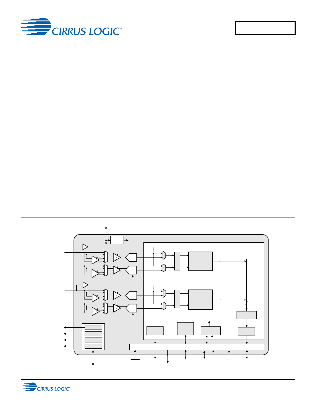
4 Functional Description
4 Functional Description
This section provides a general description of the CS53L30 architecture and detailed functional descriptions of the various
blocks that comprise the CS53L30.
4.1 Overview
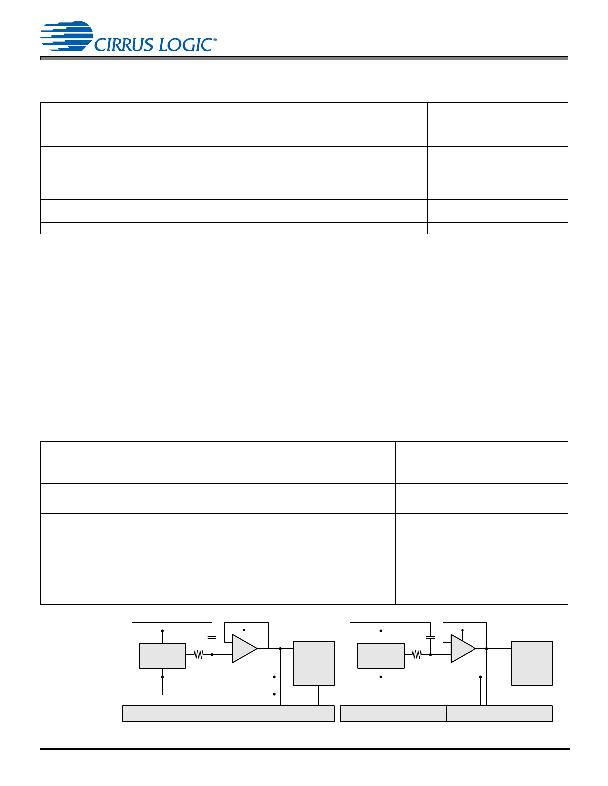
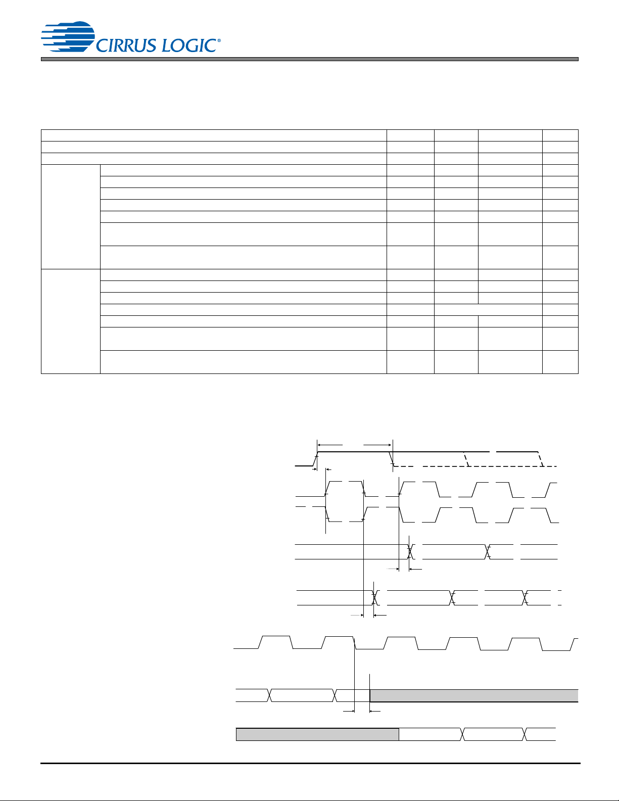
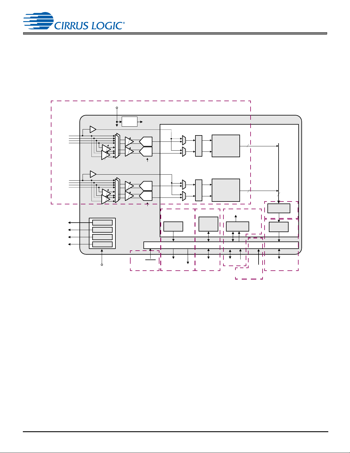
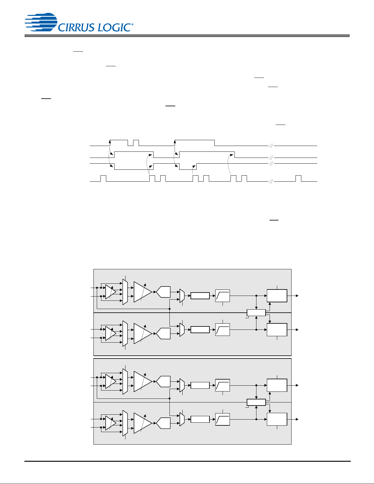
Fig. 4-1 is a block diagram of the CS53L30 with links to descriptions of major subblocks.
Figure 4-1. Overview of Signal Flow
The CS53L30 is a low-power, four-channel, 24-bit audio ADC. The ADCs are fed by fully differential analog inputs that
support mic and line-level input signals. The ADCs are designed usin g multibit delta-sigma techniques. The ADCs operate
at an optimal oversampling ratio balancing performance with power saving s. Enhanced power savings are possible when
the internal MCLK is scaled by setting MCLK_INT_SCALE (see p. 45). Table 4-2 lists supported sample rates with scaled
internal MCLK.
The serial data port operates at a selectable range of stan dard audio samp le rates as either timing master or slave. Core
timing is flexibly sourced, without the need of a PLL, by clocks with typical audio clock rates (N x 5.6448, or N x 6.1440
MHz; where N = 1 or 2), USB rates (6 or 12 MHz), or 3G and DVB rates (19.2 MHz).
The integrated LDO regulator allows the digital core to ope rate at a very low voltage , significantly reducing the CS53L30’s
overall power consumption.
The CS53L30 can operate in a system with multiple CS53L30s to increase the number of channels available. The
CS53L30s may be connected in a multidrop configuration in TDM Mode. Up to four CS53L30s can operate sim ultaneously
on the same TDM bus. Connecting together the SYNC pins of multiple CS53L30s allows operation with minimal
channel-to-channel phase mismatch across devices.
The signal to be converted can be either mic/line-level. The digital mic inputs (IN1+/DMIC1_SD, IN3+/DMIC2_SD) connect
directly to the decimators.
18 DS992F1
Page 19

The CS53L30 consists of the following blocks:
CS53L30
4.2 Resets
• Interrupts. The CS53L30 QFN package includes an open-drain, active-low interrupt output, INT
describes interrupts.
• Capture-path inputs. The analog input block, described in Section 4.4, allows selection from either analog line-level,
or analog mic sources. The selected analog source is fed into a mic preamplifier (whe n applicable ) and then into a
PGA, before entering the ADC. The pseudodifferential input configuration can provide noise rejection for
single-ended analog inputs. The digital mic inputs (IN1+/DMIC1_SD, IN3+/DMIC2_SD) connect directly to the
decimators.
• Serial ports. The CS53L30 has either two I
devices in the system such as applications processors. The serial data ports are described in Section 4.6.1. The
TDM port allows multidrop operation (i.e., tristate capable SDOUT driver) for sharing the TDM bus between multiple
devices, and flexible data structuring via control port registers.
• Synchronous sample rate converter (SRC). The SRC, described in Section 4.8, is used to bridge different sample
rates at the serial port within the digital-processing core.
• Multichip synchronization protocol. Some applications require more than four simultaneous audio channels
requiring multiple CS53L30s. In a subset of these multidevice applications, special attention to phase alignment of
audio channels is required. The CS53L30 has a synchro nization pr otocol to align all a udio chan nels a nd mi nimize
interchannel phase mismatch. Section 4.9 describes the synchronization protocol.
• Thermal overload notification. The CS53L30 can be configured to notify the system processor that its die
temperature is too high. This functionality is described in Section 4.11.
• Mute pin. The CS53L30 audio outputs can be muted with the assertion of the register-programmable MUTE pin.
The MUTE pin function can also be programmed to power-down ADCs, MICx_BIAS, etc., by setting the appropriate
bits in Section 7.17 and Section 7.18. Section 4.12 describes the MUTE pin functionality.
• Power management. Several registers provide independent powe r-down control of the analog and digital sections
of the CS53L30, allowing operation in select applications with minimal power consumption. Power management
considerations are described in Section 4.13.
• Control port operation. The control port is used to access the registers allowing the CS53L30 to be configured for
the desired operational modes and formats. The oper ation of the control port may be completely asynchronous with
respect to the audio sample rates. To avoid interference problems, the control port pins must remain static if no
operation is required. Control port operation is described in Section 4.14.
2
S output ports or one TDM output port allowing communication to other
. Section 4.3
4.2 Resets
The CS53L30 can be reset only by asserting RESET. When RESET is asserted, all registers and all state machines are
immediately set to their default values/states. No operation can begin until RESET
can begin, RESET
before the VA supply.
must be asserted at least once after the VA supply is broug ht up. The VP supply should be brought u p
is deasserted. Before normal operation
4.3 Interrupts
The status of events that may require special attention is recorded in the interrupt status register (see Section 7.36).
Interrupt status bits are sticky and read-to-clear: That is, once set, they remain set until the status register is read and the
associated interrupt condition is no longer present.
4.3.1 Interrupt Handling with the WLCSP Package
If the WLCSP package is used, events and conditions are detected in software by polling the interrupt status register. The
mask register can be ignored (see Section 7.35). Status register bits are cleared when read, as Fig. 4-2 shows. If the
underlying condition remains valid, the bit remains set even after the status register is read.
DS992F1 19
Page 20
CS53L30
Raw signal feeding
st atus re gi ster bi t
Stat us regis t er bi t
___
INT pin
Register read
signal
Stat us read val ue
0 110 10
Read Sourc e
10
Poll cycle
Interrupt
service
Extra read for
pre s ent state
Interrupt
service
Extra read for
pre s ent state
Poll cycle
Extra read for
pre s ent state
Poll cycle
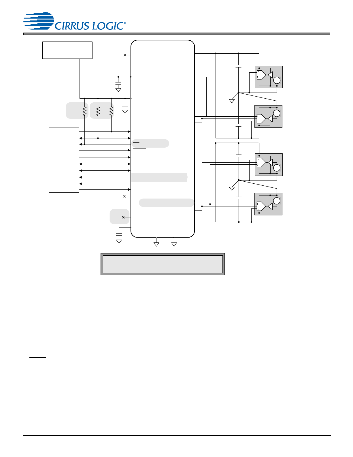
Channel 2B Data Path
Channel 2A Data Path
Channel 1B Data Path
Channel 1A Data Path
PGA
Decimator
PGA
Decimator
Digital Gain
Adjust
HPF
ADC1A
ADC1B
Digital Gain
Adjust
HPF
Noise Gate To Serial Port
PGA
Decimator
PGA
Decimator
Digital Gain
Adjust
HPF
ADC2A
ADC2B
Digital Gain
Adjust
HPF
Noise Gate To Serial Port
IN1 +/DMIC1_SD
IN 2 –
IN 1 –
IN2+
IN3 +/DMIC3_SD
IN4–
IN 3 –
IN4+
ADC1x_VOL
ADC1x_PGA_VOL
CH_TYPE
ADC1_HPF_EN
ADC1x_VOL
ADC1x_PREAMP
ADC1x_PREAMP
ADC2x_VOL
ADC2x_PGA_VOL
ADC2_HPF_EN
ADC2x_PGA_VOL
ADC2x_VOL
ADC2x_PREAMP
ADC2x_PREAMP
ADC1x_NG
ADC2x_NG
ADC1_HPF_EN
ADC1x_PGA_VOL
ADC2_HPF_EN
CH_TYPE
CH_TYPE
CH_TYPE
4.4 Capture-Path Inputs
4.3.2 Interrupt Handling with the QFN Package
The interrupt pin (INT) is implemented on the QFN package. Interrupt status bits can be individually masked by setting
corresponding bits in the interrupt mask register (see Section 7.35). The configuration of mask bits determines which
events cause the assertion of INT
:
• When an unmasked interrupt status event is detected, the status bit is set and INT
• When a masked interrupt status event is detected, the interrupt status bit is set, but INT
Once INT
remains present and the status bit is read, alth ou gh IN T
is asserted, it remains asserted until all status bits that are unmasked and set have been read. If a condition
is deasserted, the status bit remains set.
is asserted.
is not affected.
To clear any status bits set due to the initiation of a path or block, all interrupt status bits should be read after reset and
before normal operation begins. Otherwise, unmasking any previously set status bits causes INT
Figure 4-2. Example of Rising-Edge Sensitive, Sticky, Interru pt Status Bit Behavior (INT Pin in QFN only)
to assert.
4.4 Capture-Path Inputs
This section describes the line in and mic inputs. Fig. 4-3 shows the capture-path signal flow.
20 DS992F1
Figure 4-3. Capture-Path Signal Flow
Page 21
Fig. 4-4 shows details of the various analog input gain settings, including control register fields.
–6 to +12 dB
with 0.5-dB
steps
Bypas s, +10,
or +20 dB
0 or +20 dB
and/or
–96 to +12 dB
with 1-dB steps or
– dB (mute)
INx±,
(x=1,2)
Gain Adjust
Digital Gain
Adjust
ADC1xPGA
...
(Note 1)
(Note 1)
Bypas s, +10,
or +20 dB
INx±,
(x=3,4)
Gain AdjustDigital Gain
Adjust
ADC2xPGA
...
(Note 1)
(Note 1)
1. Gains within analog blocks vary with supply voltage, with temperat ure, and from part t o part. The gain val ues listed for these b locks
are typical values with nominal parts and conditions.
ADC1x_PREAMP
on p. 54
ADC1x_DIG_BOOST on p. 53
ADC1x_VOL on p. 54
ADC2x_PGA_VOL
on p. 56
ADC2x_PREAMP
on p. 56
ADC1x_PGA_VOL
on p. 54
ADC2x_DIG_BOOST on p. 55
ADC2x_VOL on p. 56
+
–
Preamp+
+
–
Preamp–
INx–
INx+
100 k
900 k
900 k
100 k
QuickRef
700 k 700 k
VA
Weak-VCM
700 k 700 k
Weak-VCM
VA
VCM
+
–
PGA
ADCx+
ADCx–
ADC1x_PGA_VOL
ADC2x_PGA_VOL
ADC1x_PREAMP
ADC2x_PREAMP
CS53L30
4.4 Capture-Path Inputs
Figure 4-4. Input Gain Paths
4.4.1 Analog Input Configurations
The CS53L30 implements fully differential analog input stages, as shown in Fig. 4-5. In addition to accepting fully
differential input signals, the inputs can be used in a pseudodifferential configuration to improve common mode noise
rejection with single-ended signals. In this configuration, a low-level referen ce signal is sensed at the ground point of the
internal mic or external mic jack and used as a pseudodifferential reference for the internal input amplifiers. Sitting between
the preamp and the PGA is an internal antialias filter with a first-order pole at 95 kHz and a first-order pole at 285 kHz.
Fig. 4-6 shows the INx interface and the related connections recommended for a fully differential internal mic. These
connections are truncated in Fig. 4-6.
Figure 4-5. Op-Amp Level Schematic—Analog Inputs
DS992F1 21
Page 22

CS53L30
Board Chip
MIC_BIAS_FILT
VP
IN1–
MIC1_BIAS
IN1+
CINM
CINM
Analog
Differential
Microphone
1.0 µF
4.7 µF
GNDA
n
Board Chip
GNDA
MIC_BIAS_FILT
VP
IN1+
IN1–
MIC1_BIAS
CINM
CINM
1.0 µF
4.7 µF
CINM
CINM
1.0 µF
CINM
CINM
1.0 µF
CINM
CINM
1.0 µF
IN2+
IN2–
MIC2_BIAS
IN3+
IN3–
MIC3_BIAS
IN4+
IN4–
MIC4_BIAS
Board ground connection made
local to the micr ophone car tridge.
Board ground connection made
local to the micr ophone car tridge.
Board ground connection made
local to the micr ophone car tridge.
Board ground connect ion made
local to the micr ophone c ar tridge.
Analog
Microphone
(see
connection
diagram)
Analog
Microphone
(see
connection
diagram)
Analog
Microphone
(see
connection
diagram)
Analog
Microphone
(see
connection
diagram)
Analog Microphone Connection
Two-wire microphone connection
Rbias
Gr ound Ring
MICx_BIAS
INx+
INx–
Three-wire microphone connection
Gr ound Ring
MICx_BIAS
INx+
INx–
4.4 Capture-Path Inputs
Figure 4-6. Fully Differential Mic Input Connections Example
Fig. 4-7 shows the IN1–IN4 interfaces and the related pseudodifferential connections recommended to achieve the best
common-mode rejection for single-ended internal mics.
22 DS992F1
Figure 4-7. Pseudodifferential Mic Input Connections Example
Page 23

CS53L30
f
c
1
2 1 M0.01 F
------------------------------------------------------ 15.9 H z==
f
c
1
2 50 k 0.1 F
---------------------------------------------------- 31.83 H z==
4.5 Digital Microphone (DMIC) Interface
4.4.2 External Coupling Capacitors
The analog inputs are internally biased to the internally generated common-mode voltage (VCM). Input signals must be
AC coupled using external capacitors (C
resistance may be combined with an external capacitor to achieve the desired cutoff frequency.
Eq. 4-1 provides an example for mic inputs.
Equation 4-1. External Coupling Capacitors—Mic Inputs
Eq. 4-2 provides an example for line inputs.
Equation 4-2. External Coupling Capacitors—Line Inputs
4.4.3 Capture-Path Pin Biasing
Capture-path pins are internally biased during normal operation. When connecting analog sources to the CS53L30, the
input must be AC-coupled with an external capacitor. These sources may bias the analog inputs:
• Quick-Ref. After an analog input is powered up, the Quick-Ref buffer charges the external capacitor with a
low-impedance bias source to minimize startup time.
• Weak VCM. When ADCx is powered up, the weak VCM biases unselected inputs to minimize coupling conditions.
• ADCx_PREAMP. When ADCx is powered up, ADCx_PREAMP biases the selected channel.
) with values consistent with the desired HPF design. The analog input
INM
See Fig. 4-5 for the location of each bias source.
4.4.4 Soft Ramping (DIGSFT)
DIGSFT (see p. 50) controls whether digital volume updates are applied slowly by stepping through each volume co ntrol
setting with a delay between steps equal to an integer number of FS
at 8 FS
When enabled, soft ramping is applied to all digital volume changes. Digital volume is affected by the following:
If digital boost is disabled and the ADC digital volume is set to any value from 0x0C to 0x7F (all equivalent to +12 dB), the
soft ramp first steps throug h the +12-dB setting s in the same manner as the remainder of the vo lume se ttings. So ft ramp
timing calculations must include these additional steps. For example, if the ADC digital volume setting is changed from
0x10 (+12 dB) to 0x00 (0 dB), the first 32 soft ramp steps from 0x10 to 0x0C do not produce any changes in digital volume,
while each of the remaining 96 steps from 0x0C (+12 dB) to 0x 00 (0 dB) ca uses a 0.125-dB re duction in digit a l volume. If
digital boost is enabled, the soft ramp does not step through the +12-dB settings.
periods. The step size is fixed at 0.125 dB.
int
1. Writing directly to the ADC digital volume registers, ADC1x_VOL or ADC2x_VOL (see p. 54 and p. 56)
2. Enabling or disabling mute by driving a signal to the MUTE pin
3. Muting that is applied automatically by the noise gate
4. Muting that is applied automatically during power up and power down
periods. The amount of delay between steps is fixed
int
4.5 Digital Microphone (DMIC) Interface
The digital mic interface can be used to collect pulse-E (PDM) audio data from the integrated ADCs of one or two digital
mics. The following sections describe how to use the inter face.
DS992F1 23
Page 24

CS53L30
DMIC_CLK
DMIC_SD
Left
(A, D ATA1)
Channel D ata
Right
(B, DATA2)
Channel D at a
Left
(A, DATA1)
Channel Data
4.5 Digital Microphone (DMIC) Interface
4.5.1 DMIC Interface Description
The DMIC interface consists of a serial-data shift clock output (DMICx_SCLK) and a serial data input (DMICx_SD).
Fig. 2-2 shows how to connect two digital mics (“Left” and “Right”) to the CS53L30. The clock is fanned out to both digital
mics, and both digital mics’ data outputs share a single signal line to the CS53 L30. To share a single line, the digi tal mics
tristate their output during one phase of the clock ( high or low part of cycle, depending on how they are configure d via their
L
/R input). The CS53L30 defaults to mono digital mic input (left channe l or rising edge of DMICx_SCLK data only). Wh en
DMIC1_STEREO_ENB or DMIC2_STEREO_ENB (see p. 52) is cleared, then both edges of DMICx_SCLK are used to
capture stereo data; Alternating between one digital mic outputting a bit of data and then the other mic outputting a bit of
data, the digital mics time domain multiplex on the signal dat a line. Contention on the data line is avoided by entering the
high-impedance tristate faster than removing it.
The DMICx_SD signal can be held low through a we ak pulldown (per Section 7.19 and Section 7.20) by its CS53L30 input.
When the DMIC interface is active, this pulling is not strong enough to affect the multiplexed data line significantly while it
is in tristate between data slots. While the interface is disabled and the data line is not driven, the weak pulling ensures
that the CS53L30 input avoids any power-consuming midrail voltage.
4.5.2 DMIC Interface Signaling
Fig. 4-8 shows the signaling on the DMIC interface. Notice how the left cha nnel (A, or DATA1 channel) data from the “Left”
mic is sampled on the rising edge of the clock and the right channel (B, or DATA2 channel) data from the “Right” mic is
sampled on the falling edge.
Figure 4-8. Digital Mic Interface Signalling
4.5.3 DMIC Interface Clock Generation
Table 4-1 lists DMIC interface serial clock (DMICx_SCLK) nominal frequencies and their derivation from the internal
master clock.
Table 4-1. Digital Mic Interface Clock Generation
Post-MCLK_DIV MCLK Rate
(MHz)
5.6448 0 X 2 2.8224 0
6.0000 0 X 2 3.0000 0
MCLK_INT_
SCALE
1 11.025 2 0.7056 0
1 8,11.025,12 2 0.7500 0
ASP_RATE
(kHz)
22.050 2 1.4112 0
44.1 2 2.8224 0
16, 22.050,
24
32, 44.1, 48 2 3.0000 0
Divide
1
Ratio
DMICx_SCLK Rate
(MHz)
41.4112 1
40.3528 1
40.7056 1
41.4112 1
41.5000 1
40.3750 1
21.5000 0
40.7500 1
41.5000 1
DMICx_SCLK_DIV
Programming
24 DS992F1
Page 25

Post-MCLK_DIV MCLK Rate
1.An X indicates that the sample rate setting does not affect DMICx_SCLK rate.
4.6 Serial Ports
Table 4-1. Digital Mic Interface Clock Generation (Cont.)
(MHz)
6.1440 0 X 2 3.0720 0
6.4000 0 X 2 3.2000 0
MCLK_INT_
SCALE
1 8, 11.025,
1 8, 11.025,
ASP_RATE
(kHz)
12
16, 22.050,
24
32, 44.1, 48 2 3.0720 0
12
16, 22.050,
24
32, 44.1, 48 2 3.2000 0
Divide
1
Ratio
DMICx_SCLK Rate
(MHz)
41.5360 1
20.7680 0
40.3840 1
21.5360 0
40.7680 1
41.5360 1
41.6000 1
20.8000 0
40.4000 1
21.6000 0
40.8000 1
41.6000 1
DMICx_SCLK_DIV
Programming
CS53L30
4.6 Serial Ports
The CS53L30 has a highly configurable serial port to communi cate audio an d voice data to and from other device s in the
system such as application processors and bluetooth transceivers.
4.6.1 I/O
The serial port interface consists of four signals:
• ASP_SCLK. Serial data shift clock
• ASP_LRCK/FSYNC. Left/right (I
2
S) or frame sync clock (TDM)
• LRCK identifies the start of each serialized data word and locates the left an d right channels within the data word
2
when I
S format is used (see Section 4.6.6).
• FSYNC identifies the start of each TDM frame.
• Toggles at external sample rate (Fs
ext
).
• ASP_SDOUTx. Serial data outputs
4.6.2 Serial Port Power-Up, Power-Down, and Tristate
The ASP has separate power-down and tristate controls for its output data paths. The serial port power, tristate, and TDM
control is done through ASP_3ST, ASP_TDM_PDN, and the respective ASP_SDOUTx_PDN bit. Separating power state
controls helps minimize power consumption when the output port is not in use.
• ASP_SDOUTx_PDN. If the SDOUT functionality of a serial port is not required, the SDOUT data path can be
powered down by setting ASP_SDOUTx_PDN. The ASP_SDOUTx pin is Hi-Z when ASP_SDOUTx_PDN is set; it
does not tristate the serial port clock.
• ASP_3ST. See Section 4.6.3 for details.
• ASP_TDM_PDN. When ASP_TDM_PDN = 1, the ASP serial port is configured to operate in I
TDM_PDN = 0, ASP is configured to operate in TDM Mode and ASP_SDOUT2 is Hi-Z.
To facilitate clock mastering in TDM Mode, while not sending data, ASP_TDM_PDN and all ASP_TX_ENABLEy
bits must be cleared to prevent wasting power to drive the output nets. To save power when no TDM TX slots are
used, ASP_SDOUT1 is automatically tristated.
2
S Mode. When ASP_
Master/slave operation is controlled only b y the M/S
bit setting and is done irrespective of the setting of the ASP_SDOUTx_
PDN, and ASP_3ST bits.
DS992F1 25
Page 26

CS53L30
CODEC Interface
Transmitting Device
#1
Transmitting
Device #2
Receiving Device
ASP_SDOUTx
ASP_SCLK,
ASP_LRCK
ASP_3ST
Transmitting
Device
#2
CODEC Interface
Transmitting Device
#1
ASP_SDOUTx
ASP_SCLK,
ASP_LRCK
ASP_3ST
Receiving Device
4.6 Serial Ports
4.6.3 High-Impedance Mode
The serial port may be placed on a clock/data bus that allows multiple masters, without a need for external buffers. The
ASP_3ST bit places the internal buffers for the serial port interface signals in a high-impedance state, allowing another
device to transmit clocks and data without bus contention. If the CS53L30 serial por t is a timing slave, its ASP_SCLK and
ASP_LRCK/FSYNC I/Os are always inputs and are thus unaffected by the ASP_3ST control.
In Slave Mode, setting ASP_3ST tristates the ASP_SDOUTx pins. In Master Mode, setting ASP_3ST tristates the ASP_
SCLK, ASP_LRCK/FSYNC, and ASP_SDOUTx pins. Before setting an ASP_3ST bit, the associated serial port must be
powered down and must not be powered up until the ASP_3ST bit is cleared. Below is the recommended tristate
sequence.
Sequence for initiating tristate:
1. Set the ASP_SDOUT1_PDN and ASP_SDOUT2_PDN bits.
2. If the ASP is in TDM Mode, set the ASP_TDM_PDN bit.
3. Set the ASP_3ST bit.
Sequence for removing tristate:
1. Clear the ASP_3ST bit.
2. If TDM Mode is desired, clear the ASP_TDM_PDN bit.
3. Clear the ASP_SDOUT1_PDN and ASP_SDOUT2_PDN bits.
Fig. 4-9 and Fig. 4-10 show serial port interface busin g fo r master and slave timing serial-port use cases.
Figure 4-9. Serial Port Busing when Master Timed Figure 4-10. Serial Port Busing when Slave Timed
4.6.4 Master and Slave Timing
Serial ports can independently operate as the master of tim ing or as a slave to another device ’s timing. When mastering,
ASP_SCLK and ASP_LRCK/FSYNC are outputs; when slaved, they are inputs. ASP_M/S
Mode.
In Master Mode, ASP_SCLK and ASP_LRCK/FSYNC clock outputs are either derived from the internal MCLK or taken
directly from its source, MCLK.
determines the Master/Slave
Table 4-2 lists supported interface sample rates (Fs
registers to derive the desired Fs
26 DS992F1
ext
) for each supported MCLK and documents how to program the
ext
.
Page 27

CS53L30
4.6 Serial Ports
4.6.5 Serial-Port Sample Rates
Table 4-2 lists the supported sample rates. Before making changes to any clock settin g or frequen cy, the device must be
powered down by setting either the PDN_ULP or PDN_LP bit.
v
Table 4-2. Supported Master Clocks and Sample Rates
MCLK
(MHz)
EXT
MCLK
INT
(MHz)
6.0000 6.0000 (MCLK_
DIV = 00)
12.0000 6.0000
5.6448 5.6448
11.2896 5.6448
(MCLK_
DIV = 01)
(MCLK_
DIV = 00)
(MCLK_
DIV = 01)
INTERNAL_FS_RATIO
Setting(MCLK
INT
/FS
MCLK_INT_SCALE
)
MCLK
INT
INT
Scaling
ASP_RATE
0 0 (disabled) 0001 48.000 8.000 750
1 (4) 0001 12.000 8.000 750
0 (disabled) 0010 48.000 11.025 80000/147
1 (4) 0010 12.000 11.025 80000/147
X 0011 48.000 11.029
0 (disabled) 0100 48.000 12.000 500
1 (4) 0100 12.000 12.000 500
0 (disabled) 0101 48.000 16.000 375
1 (2) 0101 24.000 16.000 375
0 (disabled) 0110 48.000 22.050 40000/147
1 (2) 0110 24.000 22.050 40000/147
X 0111 48.000 22.059
0 (disabled) 1000 48.000 24.000 250
1 (2) 1000 24.000 24.000 250
X 1001 48.000 32.000 187.5
X 1010 48.000 44.100 20000/147
X 1011 48.000 44.118
X 1100 48.000 48.000 125
0 0 (disabled) 0001 48.000 8.000 1500
1 (4) 0001 12.000 8.000 1500
0 (disabled) 0010 48.000 11.025 160000/147
1 (4) 0010 12.000 11.025 160000/147
X 0011 48.000 11.029
0 (disabled) 0100 48.000 12.000 1000
1 (4) 0100 12.000 12.000 1000
0 (disabled) 0101 48.000 16.000 750
1 (2) 0101 24.000 16.000 750
0 (disabled) 0110 48.000 22.050 80000/147
1 (2) 0110 24.000 22.050 80000/147
X 0111 48.000 22.059
0 (disabled) 1000 48.000 24.000 500
1 (2) 1000 24.000 24.000 500
X 1001 48.000 32.000 375
X 1010 48.000 44.100 40000/147
X 1011 48.000 44.118
X 1100 48.000 48.000 250
1 0 (disabled) 0100 44.100 11.025 512
1 (4) 0100 11.025 11.025 512
0 (disabled) 1000 44.100 22.050 256
1 (2) 1000 22.050 22.050 256
X 1100 44.100 44.100 128
1 0 (disabled) 0100 44.100 11.025 1024
1 (4) 0100 11.025 11.025 1024
0 (disabled) 1000 44.100 22.050 512
1 (2) 1000 22.050 22.050 512
X 1100 44.100 44.100 256
Fs
INT
(kHz)
LRCK (Fs
(kHz)
EXT
2
2
2
2
2
2
)
MCLK
LRCK Ratio
544
272
136
1088
544
272
EXT
/
1
DS992F1 27
Page 28
Table 4-2. Supported Master Clocks and Sample Rates (Cont.)
MCLK
(MHz)
6.1440 6.1440 (MCLK_
12.2880 6.1440
19.2000 6.4000
1.The internal synchronous SRC guarantees the MCLK
PCM master must provide the exact MCLK/LRCK ratio.
2.Supported only if CS53L30 is a PCM bus slave.
EXT
MCLK
(MHz)
DIV = 00)
(MCLK_
DIV = 01)
(MCLK_
DIV = 10)
INT
INTERNAL_FS_RATIO
Setting(MCLK
/FS
INT
1 0 (disabled) 0001 48.000 8.000 768
1 0 (disabled) 0001 48.000 8.000 1536
1 0 (disabled) 0001 50.000 8.000 2400
CS53L30
4.6 Serial Ports
MCLK_INT_SCALE
)
MCLK
INT
/LRCK ratio when the CS53L30 is a PCM bus master. If the CS53L30 is a PCM slave, the
EXT
Scaling
INT
1 (4) 0001 12.000 8.000 768
0 (disabled) 0010 48.000 11.025 81920/147
1 (4) 0010 12.000 11.025 81920/147
0 (disabled) 0100 48.000 12.000 512
1 (4) 0100 12.000 12.000 512
0 (disabled) 0101 48.000 16.000 384
1 (2) 0101 24.000 16.000 384
0 (disabled) 0110 48.000 22.050 40960/147
1 (2) 0110 24.000 22.050 40960/147
0 (disabled) 1000 48.000 24.000 256
1 (2) 1000 24.000 24.000 256
X 1001 48.000 32.000 192
X 1010 48.000 44.100 20480/147
X 1100 48.000 48.000 128
1 (4) 0001 12.000 8.000 1536
0 (disabled) 0010 48.000 11.025 163840/147
1 (4) 0010 12.000 11.025 163840/147
0 (disabled) 0100 48.000 12.000 1024
1 (4) 0100 12.000 12.000 1024
0 (disabled) 0101 48.000 16.000 768
1 (2) 0101 24.000 16.000 768
0 (disabled) 0110 48.000 22.050 81920/147
1 (2) 0110 24.000 22.050 81920/147
0 (disabled) 1000 48.000 24.000 512
1 (2) 1000 24.000 24.000 512
X 1001 48.000 32.000 384
X 1010 48.000 44.100 40960/147
X 1100 48.000 48.000 256
1 (4) 0001 12.500 8.000 2400
0 (disabled) 0010 50.000 11.025 256000/147
1 (4) 0010 12.500 11.025 256000/147
0 (disabled) 0100 50.000 12.000 1600
1 (4) 0100 12.500 12.000 1600
0 (disabled) 0101 50.000 16.000 1200
1 (2) 0101 25.000 16.000 1200
0 (disabled) 0110 50.000 22.050 128000/147
1 (2) 0110 25.000 22.050 128000/147
0 (disabled) 1000 50.000 24.000 800
1 (2) 1000 25.000 24.000 800
X 1001 50.000 32.000 600
X 1010 50.000 44.100 64000/147
X 1100 50.000 48.000 400
ASP_RATE
Fs
INT
(kHz)
LRCK (Fs
(kHz)
EXT
)
MCLK
LRCK Ratio
EXT
/
1
4.6.6 I2S Format
I2S format offers the following:
• Up to 24 bits/sample of stereo data can be transferred (see Section 4.6.6.1).
• Master or slave timing may be selected.
• LRCK (i.e., ASP_LRCK/FSYNC) identifies the start of a new sample word and the active stereo channel (A or B).
• Data is clocked out of the ASP_SDOUTx output using the falling edge of SCLK (i.e., ASP_SCLK).
• Bit order is MSB to LSB.
Fig. 4-11 shows the signaling for I
28 DS992F1
2
S format.
Page 29
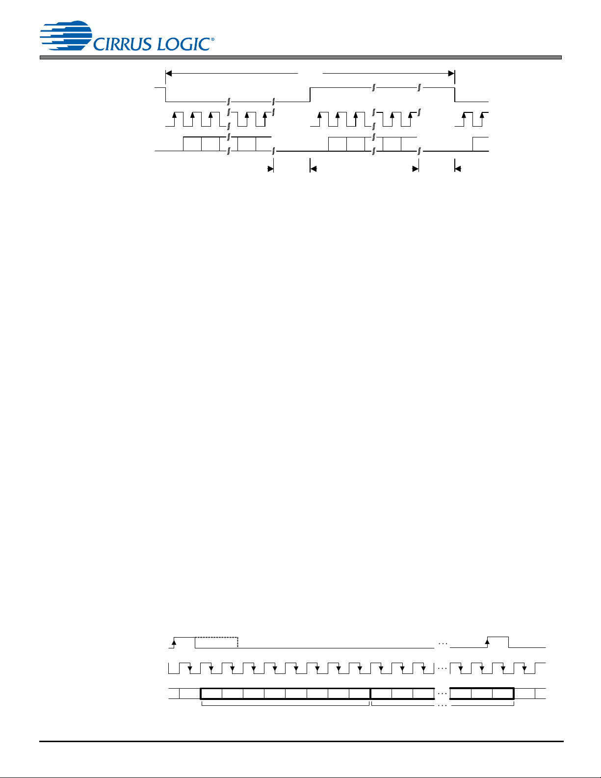
CS53L30
LRCK
SCLK
ASP_SDOUTx
MSB MSB-1 LSB +1 LSB
1/Fs
ext
Note:
x = 1, 2
MSB MSB-1 LSB +1 LSB MSB
SCLK may
stop or
continue
t
extraA
=
None to
some time
SCLK may
stop or
continue
t
extraB
=
None to
some time
Left (A) Channel Right (B) Channel
0:7 0:6 0:5 0:4 0:3 0:2 0:1 0:0 1:7 1:6 1:5 m:2 m:1 m:0 0:7
FSYNC
SCLK
(ASP_SCLK_ I NV = 0, default)
SDOUT
(SHIFT_LEFT = 0, default)
Slot 0 Slot 1
m:0
Slot m
4.7 TDM Mode
Figure 4-11. I2S Format
4.6.6.1 I2S Format Bit Depths
I2S interface data word length (see Section 4.6.6) is ambiguous. Fortunately, the I2S format is also left justified, with
MSB-to-LSB bit ordering, negating the need for a word-length control register. If at least 24 serial clocks are present per
channel sample, the CS53L30 always sends 24-bit data. If fewer clocks are present, it outpu ts as many bits as the re are
clocks. If more are present, it transmits zeros for any clock cycles after the 24th bit. The receiving device is expected to
load data in MSB-to-LSB order until its word depth is reached, at which point it must discard an y re ma in ing LSBs.
4.7 TDM Mode
The ASP can operate in TDM Mode, which includes the following features:
• Defeatable SDOUT driver for sharing the TDM bus between multiple devices
• Flexible data structuring via control port registers
• Clock master and slave modes
4.7.1 Bus Format and Clocking
The serviceable TDM data stream is defined as 48 8-bit slots, as clocked by SCLK (i.e., ASP_SCLK). Unlike op erating the
port in I
scaled when the device is operating as a clock slave and is not scaled when the device is operating as a clock master. For
example, if a 6.400-MHz clock is used for SCLK, a 16-kHz sample rate would result in 48 available slots or 16 available
24-bit (3-slot) flows with 16 unused SCLK cycles per 400 SCLK cycles (16-kHz frame). If the sample rate were changed
to 8 kHz, the bus would support 48 possible 8-bit slots, but would result in 416 unused SCLK cycles per 800 SCLK cycles
with = 6.400 MHz.
TDM frames are bounded by the FSYNC signal (i.e., ASP_LRCK/FSYNC). The placement of the first bit applied to SDOUT
(i.e., ASP_SDOUT1) in a given TDM frame is programmable using the SHIFT_LEFT bit. By default, the first bit of the TDM
frame is driven on the second rising edge of SCLK following t he rising edge o f FSYNC. The first bit of the TDM frame can
be moved up a half SCLK cycle earlier by setting the SHIFT _LEFT bit. SHIFT_LEFT an d ASP_SCLK_INV can be used in
conjunction to achieve a frame start (i.e., first data bit driven out) on the first rising edge of SCLK as shown in Fig. 4-17.
The high time of FSYNC is also programmable by programming LRCK_TPWH[10:3] (see Section 7.15), LRCK_
TPWH[2:0], and LRCK_50_NPW (see Section 7.16).
Fig. 4-12–Fig. 4-15 show the four possible TDM formats achievable using the ASP_SCLK_INV and SHIFT_LEFT bits. The
number of unused SCLK cycles in each case is zero. Fig. 4-16 shows an example of the resulting TD M fra m e str ucture
when there are unused SCLK cycles in the frame.
2
S Mode, where SCLK is scaled to always be approximately 64 bits per LRCK toggle, SCLK is not requ ired to be
DS992F1 29
Figure 4-12. TDM Format—ASP_SCLK_INV = 0, SHIFT_LEFT = 0
Page 30

Figure 4-13. TDM Format—ASP_SCLK_INV = 0, SHIFT_LEFT = 1
0:7 0:6 0:5 0:4 0:3 0:2 0:1 0:0 1:7 1:6 1:5 m:2 m:1 m:0 0:7
FSYNC
SCLK
(ASP_SCLK_INV = 0, defaul t)
SDOUT
(SHIFT _LEFT = 1)
Slot 0 Slot 1
m:0
Slot m
0:7 0:6 0:5 0:4 0:3 0:2 0:1 0:0 1:7 1:6 1:5 m:2 m:1 m:0 0:7
FSYNC
SCLK
(ASP_SCLK_INV = 1)
SDOUT
(SHIFT _LEFT = 0, default )
Slot 0 Slot 1
m:0
Slot m
0:7 0:6 0:5 0:4 0:3 0:2 0:1 0:0 1:7 1:6 1:5 m:2 m:1 m:0 0:7
FSYNC
SCLK
(ASP_SCLK_INV = 1)
SDOUT
(SHIFT _LEFT = 1)
Slot 0
Slot 1
m:0
Slot m
0:70:7 0:6 0:5 0:4 0:3 0:2 0:1 0:0 1:7 1:6 1:5 m:2 m:1 m:0
FSYNC
SCLK
(ASP_SCLK_INV = 0, default)
SDOUT
(SHIFT_ LEFT = 0, default)
Slot 0 Slot 1
m:0
Slot m
Unused clocks
In Master Mode, all unused
SCLKs are driven.
In Slave Mode, bursted
SCLK is supported.
Figure 4-14. TDM Format—SCLK_INV = 1, SHIFT_LEFT = 0
CS53L30
4.7 TDM Mode
In TDM Master Mode, SCLK is a buffered version of MCLK and is not scaled to FS
and because the number of available bits on a given bus is defined by the ratio of SCLK to sample rate (SCLK/f
the TDM bus use can vary. As Table 4-3 shows, applying the SCLK/f
sample rates of the device results in different numbers of available slots as well as different numbers of unused bits.
Table 4-3. Slot Count and Resulting Unused Clock Cycles for Supported SCLK and Sample Rates
SCLK Frequency [MHz] FSYNC Sample Rate [kHz] Number of Available Slots Resulting Number of Unused SCLK Cycles
5.6448 11.025 48 128
11.2896 11.025 48 640
30 DS992F1
Figure 4-15. TDM Format—SCLK_INV = 1, SHIFT_LEFT = 1
Figure 4-16. TDM Format—Unused SCLK Cycles
as it is in I2S Mode. Because of this,
ext
relationship to the supported clocks and
FSYNC
22.050 32 0
44.100 16 0
22.050 48 128
44.100 32 0
),
FSYNC
Page 31

CS53L30
4.7 TDM Mode
Table 4-3. Slot Count and Resulting Unused Clock Cycles for Supported SCLK and Sample Rates (Cont.)
SCLK Frequency [MHz] FSYNC Sample Rate [kHz] Number of Available Slots Resulting Number of Unused SCLK Cycles
6.0000 8.000 48 366
11.025 48 160
12.000 48 116
16.000 46 7
22.050 34 0
24.000 31 2
32.000 23 4
44.100 17 0
48.000 15 5
12.0000 8.000 48 1116
11.025 48 704
12.000 48 616
16.000 48 366
22.050 48 160
24.000 48 116
32.000 46 8
44.100 34 0
48.000 31 2
6.1440 8.000 48 384
11.025 48 173
12.000 48 128
16.000 48 0
22.050 34 6
24.000 32 0
32.000 24 0
44.100 17 3
48.000 16 0
12.2880 8.000 48 1152
11.025 48 731
12.000 48 640
16.000 48 384
22.050 48 173
24.000 48 128
32.000 48 0
44.100 34 6
1
6.4000
1. 6.4 MHz is the highest SCLK frequency allowed if MCLK_19MHZ_EN is set.
48.000 32 0
8.000 48 416
11.025 48 196
12.000 48 149
16.000 48 16
22.050 36 2
24.000 33 2
32.000 25 0
44.100 18 1
48.000 16 5
4.7.2 Bursted SCLK
After all the data is sent on the TDM bus, it is not necessary to continue to toggle SCLK for the remaining unused slots.
Not toggling SCLK after all data is sent and received saves power, by avoiding driving the output and clo ck capacitances
unnecessarily. When the device is operating as a timing slave, bursted SCL K is naturally supporte d, since data is clocked
out only when SCLK toggles. When the device is operating as a timing master, bursted SCLK is not supported.
DS992F1 31
Page 32

4.7.3 Transmitting Data
TDM Transmit
ASP_SDOUT1
Data Registers
ASP _C H1 Dat a
ASP_CHx Data
ASP _C H4 Dat a
TD M Slot Ass ignm ent
Control
SCLK
ASP_CH4_TX_LOC
FSYNC
ASP_CHx_TX_LOC
ASP_CH1_TX_LOC
ASP_TX_ENABLE[47:0]
48-bit T D M Slot
Enable Cont rol
ASP_CH4_TX_STATE
ASP_CHx_TX_STATE
ASP_CH1_TX_STATE
Fig. 4-17 shows the TDM transmit subblock.
Figure 4-17. TDM Transmit Subblock Diagram
CS53L30
4.7 TDM Mode
4.7.3.1 Transmit Data Structuring
Data registers are assigned to slots using the ASP_CHx_LOC, ASP_CHx_TX_STATE, and the ASP_TX_ENABLE
controls. The ASP_CHx_TX_LOC control (“x” is the channel number) determines which of the available 48 slots the da ta
set should be loaded into, MSB first. If an internal data register is not to be transmitted outside of the part, clear ASP_CHx_
TX_STATE. ASP_TX_ENABLE determines which of the loaded slots are transmitted on the ASP_SDOUT1 pin.
The SDOUT driver enters a Hi-Z state for disabled slots. An important implication of disabling slots is that if a disabled slot
lies between two enabled slots, the SDOUT driver enters a Hi-Z state during the disabled slot segment, but the data for
both enabled slots is transmitted. For example, if a 24-bit data set is assigned to Slots 0–2, but the TX_ENABLE1 bit is
cleared, the highest 8 bits of data are sent in Slot 0, the SDOUT driver enters a Hi- Z state during Slot 1 ( the middle 8 bits
of data are lost), and the lowest 8 bits of data are sent in Slot 2.
If the start slot location of a data set overlaps one or more slots of a previous data set, the new data set has higher priorit y
(e.g., if the Channel 1 data set starts in Slot 0 and the Channel 2 data set starts in Slot 1, Slot 1 contains Channel 2 data).
If two or more data sets are allocated to use the same slot start location, the lowest numbered channel has the highest
priority (e.g., the Channel 2 data set has higher priority than the Channel 3 and Channel 4 data sets).
4.7.3.2 Transmit Data Register Bit Depths
The bit depths of the internal data registers are 24 bits. The configurability of the CS53L30’s TDM data structure makes it
possible to allocate the data register to a different bit depth on the TDM bus than that of its respective internal data register.
If a data set is allocated fewer bits than its internal data register bit depth, the data is truncated. The transmission of the
slots that would have held the excess data can be disabled.
If the data set is allocated a bit depth larger than the bit depth of its internal data registers, zeros are transmitted in the
lower LSBs after all the data in the data register has been transmitted.
4.7.3.3 TDM Bus Sharing among Multiple Devices
Bus sharing is supported for device transmit. Sharing the bus among multiple devices that are attempting to transmit data
simultaneously is not inherent to the TDM architecture. Since the devices may likely be attempting to drive different data
from one another, this presents an opportunity for bus contention.
To prevent bus contention, the data from internal data registers must be allocated to different slots within the TDM stream
using each device’s ASP_CHx_TX_LOC controls.
32 DS992F1
Page 33

CS53L30
4.8 Synchronous Sample-Rate Converter (SRC)
To maximize bus usage, the device supports hand-off between devices in a half clock cycle, which means no clock cycles
have to be sacrificed during the hand-off between two d evices. This behavior is shown in Table 3-12. If SHIFT_LEFT (see
p. 45) is set, the hand-off between two devices has no margin and brief bus contention may occur.
As shown in Table 3-12, the transmission of the last LSB before a disabled slot transitions to Hi-Z earlier than a normal
transition to allow more time for the data being driven by the succeeding device to b ecome stable on the bus before being
clocked in by the receiver. This minimizes the risk of bus contention and ensures that any data loss affects only the LSB
of a given data set, not the MSB. Bus sharing after the 48-slot window is not supported and SDOUT will be driven for up
to 16 SCLKs following the 48th slot. After the 16th SCLK, SDOUT is driven low for the remainder of the frame. The
expected behavior follows:
• As long as SCLK is toggling, data transfers of up to 3 bytes can be initiated from any of the 48 slots, including the
last two (Slots 46–47).
If a transfer is configured from either of the last two slots (Slot 46 or 47), SDOUT drives all 24 bits of specified data,
after which SDOUT is driven low.
• If Slot 47 is not enabled, SDOUT is set to Hi-Z and remains at Hi-Z until the end of the frame.
4.8 Synchronous Sample-Rate Converter (SRC)
The CS53L30 includes dual decimation-mode synchronous stereo SRC to bridge potentially different sample rates in the
system. Multirate digital signal-processing techniques are used to conceptually up-sample the incoming data to a very high
rate and then down-sample to the outgoing rate. Internal filter ing is designed so that a full input audio b andwidth of 20 kHz
is preserved if the output sample rate is greater than or equal to 44.1 kHz. Any jitter in the incoming signal has little effect
on the dynamic performance of the rate converter and has no influence on the output clock.
The MCLK to LRCK ratios defined in Table 4-2 must be followed to achieve the sample rates in either Master or Slave
Mode. The coefficients of a linear time varying filter are pr ede term ined to pr odu ce the ou tp ut sam ple ra tes in Table 4-2 if
the MCLK to LRCK ratios are used.
The gain from INx to SDOUT through the SRC is dependent on output sample rate (i.e., LRCK frequency) and MCLK
frequency. Table 4-4 shows the gain with a 1-kHz full scale input over the supported sample rates and MCLK frequencies.
Table 4-4. Synchronous SRC Gain Versus Sample Rate
MCLK
5.6448, 11.2896 11.025 –0.173
6.0000, 6.1440, 12.0000, 12.2880 8.000 –0.313
1.Gain with a 1-kHz, full scale input sine wave, 0-dB gain preamp setting, and 0-dB PGA gain
setting, ADCx_NOTCH_DIS = 1, ADCx_HPF_EN = 0.
(kHz) LRCK (kHz) Gain (dB)
ext
22.050 –0.170
44.100 –0.168
11.025 –0.291
12.000 –0.172
16.000 –0.307
22.050 –0.288
24.000 –0.169
32.000 –0.305
44.100 –0.287
48.000 –0.167
19.2000 8.000 –0.383
11.025 –0.241
12.000 –0.231
16.000 –0.376
22.050 –0.236
24.000 –0.231
32.000 –0.374
44.100 –0.238
48.000 –0.231
1
DS992F1 33
Page 34

CS53L30
4.9 Multichip Synchronization Protocol
4.9 Multichip Synchronization Protocol
Due to the multidrop capability of the CS53L30 TDM bus, it is conceivable to employ up to four CS53L30 chips to allow
up to 16 channels of audio capture. Extra care and sequencing steps have to be taken to ensure that the multichip
configuration meets the channel-to-channel phase matching specification across chips when using multiple CS53L30
chips in a system. Below is the recommended sequence to minimize phase mismatch across channels/chips. Any
deviation from this procedure causes deterministic, as well as nondeterministic, phase differences across chips and the
channel-to-channel phase mismatch specifications in Table 3-5 cannot be guaranteed. The SYNC pins of all devices must
be connected directly at the board level.
Synchronization sequence:
1. Release RESET
to all devices.
2. Configure the control port of all devices.
3. Clear PDN_ULP and/or PDN_LP in all devices.
4. Set the SYNC_EN bit of one of the devices only (the “initiator” device).
5. After successful synchronization, the SYNC_DONE status bit (see p. 57) is set on all connected CS53L30s that
have received the SYNC protocol (including the initiator device).
Alternate synchronization sequence:
1. Release RESET
to all devices.
2. Configure the control port of all devices.
3. Set the SYNC_EN bit of one of the devices only (the “initiator” device).
4. Clear PDN_ULP and/or PDN_LP in all devices except the initiator device.
5. Clear PDN_ULP and/or PDN_LP in the initiator device.
6. After successful synchronization, the SYNC_DONE status bit (see p. 57) is set on all connected CS53L30s that
have received the SYNC protocol (including the initiator device).
4.10 Input Path Source Selection and Powering
Table 4-5 describes how the CH_TYPE, ADCxy_PDN, and DMICx_PDN controls affect the CS53L30. The DMICx_PDN
control only affects the state of the digital mic interface clock.
Table 4-5. ADCx/DMICx Input Path Source Select and Digital Power States (Where x = 1 or 2)
Control Register States Channel A Input Path Channel B Input Path
CH_TYPE DMICx_PDN ADCxA _P DN ADCxB_PDN Data Source Power State Data Source P o wer State
1000DMICxOnDMICxOnOn
1001DMICxOn—OffOn
1010—OffDMICxOnOn
1011—Off—OffOn
0100ADCxAOnADCxBOnOff
0101ADCxAOn—OffOff
0110—OffADCxBOnOff
0111—Off—OffOff
DMICx_SCLK
4.11 Thermal Overload Notification
The CS53L30 can be configured to notify the system processor that its die temperature is too hig h. The processor can use
this notification to prevent damage to the CS53L30 and to other devices in the system. When notified, the processor should
react by powering down CS53L30 (and/or other devices in the system) partially or entirely, depending on the extent to
which the CS53L30’s power dissipation is the cause of its excessive die temperature. The CS53L3 0 is a low-power device
and any thermal overload is likely coming from elsewhere in the system.
34 DS992F1
Page 35

CS53L30
4.12 MUTE Pin
To use thermal overload notification, do the following:
1. Enable the thermal-sense circuitry by programming THMS_PDN (see p. 48).
2. Set M_THMS_TRIP (see p. 57) if an interrupt is desired when THMS_TRIP toggles from 0 to 1.
3. Monitor (read after interrupt [QFN only] or poll) the thermal overload interrupt status bit and respond accordingly.
Except for the associated status bit, the operation of the CS53L30 is not affected by the thermal overload notification.
4.12 MUTE Pin
If MUTE is asserted, all four audio channels are muted. In addition, other circuits can be powered down; for exampl e,
power down all ADCs and MIC_BIAS outputs or individual ADC channels or MIC_BIAS outputs by prog ramming the MUTE
pin control registers (Section 7.17 and Section 7.18 list programming options).
If DIGSFT (see p. 50) is set when the MUTE pin is asserted or deasserted, the corresponding volume ramp occurs before
the power-state change.
4.13 Power-Up and Power-Down Control
The CS53L30 offers the following for managing power:
• The RESET
•The PDN_ULP bit (see p. 47)
•The PDN_LP bit (see p. 47)
• Individual x_PDN bits
In addition, the MUTE pin can also be programmed to affect any or all of the PDNs. When RESET
are powered down and reset to their default values. (See Table 3-14 for minimum RESET
(PDN_ULP = 1 or PDN_LP = 1), all blocks except the I
ultralow-power operation as it powers down the internal bandgap, VREF, VCM, weak VCM, as well as the ADCs, state
machines, etc. PDN_LP is used for low-power operation and only powers down the ADCs, state machines, etc. PDN_ULP
and PDN_LP can be used to control the sequence of what is powered in the CS53L30. When both PDN_ULP and PDN_
LP are cleared, all blocks are powered up depending on the individual x_PDN bits. If both PDN_ULP and PDN_LP are
cleared simultaneously, the bandgap, VREF, and VCM circuits are no t available for approximately 20 ms. To effect a more
deterministic power-up of the ADCs, internal dividers, state machines, etc., the following sequence is recommended:
1. Set both PDN_ULP and PDN_LP.
2. Release PDN_ULP.
3. Wait 50 ms before releasing PDN_LP.
pin
is asserted, all blocks
pulse width.) In power down
2
C control port are powered down. PDN_ULP is used for
4.14 I2C Control Port
The control port is used to access the registers allowing the device to be configured for the desired operational modes and
formats. The operation of the control port may be completely asynchronous with respect to the audio sample rates.
However, to avoid potential interference problems, the control port pins should remain static if no operation is required.
SDA is a bidirectional data line. Data is clocked into and out of the CS53L30 by the clock, SCL. The signal tim ings for read
and write cycles are shown in Fig. 4-18–Fig. 4-20. A Start condition is defined as a falling transition of SDA while the clock
is high. A Stop condition is defined as a rising transition of SDA while the clock is high. All ot her tra nsitions of SDA occu r
while the clock is low.
The first byte sent to the CS53L30 after a Start condition consists of a 7-bit chip address field and a R/W
read, low for a write) in the LSB. To communicate with the CS53L30, the chip address field is dependent upon the state
of AD0 and AD1 after RESET
1001 010 if AD1,0 = 10, and 1001 011 if AD1,0 = 11.
DS992F1 35
has been deasserted and should match 1001 000 if AD1,0 = 00, 1001 001 if AD1,0 = 01,
bit (high for a
Page 36

CS53L30
4 5 6 7 24 25
SCL
Chip Address (Write) MAP Byte Data
Data
START
STOP
ACKACK
SDA
0 1 2 3 8 9 12 16 17 18 19 10 11 13 14 15 27 28
26
Data
SDA
Source
Master Master Master
Pullup
Slave Slave Slave Slave
Master
Pullup
ACK ACK
MAP Addr = X
INCR = 1
R/W = 0
Data to
Addr X+1
Data to
Addr X+n
Master Master
Slave
Data to
Addr X
Addr = 1001010
6 4325710643257106710 67106710
SCL
SDA
SDA
Source
Pullup
DATA
STOP
ACK
ACK
CHIP ADDRESS (READ)
START
NO
258 9 184 5 6 7 0 1 2 3 16 17 34 35 36
ACK
R/W = 1
DATA DATA
Data from
Addr X+n+1
Data from
Addr X+n+2
Data from
Addr X+n+3
Master
Slave Slave Slave
Master Master Master Pullup
27
Addr = 1001010
64325710707070
4.14 I2C Control Port
AD0 and AD1 are the logic state of the ASP_SDOUT2/AD0 and DMIC2_SCLK/AD1 pins, which are pulled to the supply
or ground. These pins configure the I²C device address upon a device power up, after RESET
have internal pull-down resistors, allowing for the d efault I
2
C address with no external components. If an I2C address other
than the default is desired, then external resistor termination to VA is required. The minimu m resistor va lue allowed is 10
k. The time constant resulting from the pull-up or pull-down resistor and the total net capacitance sho uld be considered
when determining the time required for the pin voltage to settle before RESET
specifications on internal pull-down resistance and V
and VIL voltage.
IH
is deasserted. See Table 3-14 for
The next byte is the memory address pointer (MAP); the 7 LSBs of the MAP byte select the address of the register to be
read or written to next. The MSB of the MAP byte, INCR, selects whether autoincrementing is to be used (INCR = 1),
allowing successive reads or writes of consecutive registers.
Each byte is separated by an acknowledge bit. The ACK bit is output from the CS53L30 after each input byte is read and
is input to the CS53L30 from the microcontroller after each transmitted byte.
If the operation is a write, the bytes following the MAP byte are written to the CS53L30 register address indicated by the
sum of the last-received MAP and the number of times the MAP has automatically incremented since the MAP was last
received. Fig. 4-18 shows a write pattern with autoincrementing.
is deasserted. These pins
Figure 4-18. Control Port Timing, I2C Writes with Autoincrement
If the operation is a read, the contents of the register indicated by the sum of the last-received MAP and the number of
times the MAP has automatically incremented since it was last received, are output in the next byte. Fig. 4-19 shows a
read pattern following the write pattern in Fig. 4-18. Notice how read addresses are based on the MAP byte from Fig. 4-18.
Figure 4-19. Control Port Timing, I2C Reads with Autoincrement
If a read address not based on the last received MAP address is desired, an aborted write operation can be used as a
preamble that sets the desired read address. Thi s preamble te chnique is shown in Fig. 4-20: A write operation is aborted
(after the acknowledge for the MAP byte) by sending a stop condition.
36 DS992F1
Page 37

CS53L30
SCL
Chip Address (Write) MAP Byte Data
START
ACK
STOP
ACK
ACKACK
SDA
Chip Address (Read )
START
NO
16 8 9 12 13 14 15 4 5 6 7 0 1 20 21 22 23 24
26 27 28
2 3 10 11 17 18 19 25
ACK
STOP
MAP Addr = Z
INCR = 1
Addr = 1001010
R/W = 0
R/W = 1
Data Data
Data from
Addr Z
Data from
Addr Z+1
Data from
Addr Z+n
SDA
Source
Master Master Master
Pullup
Slave Slave
Slave Slave Slave
Master Mast er Master
Pullup
Addr = 1001010
643257106432571064325710707070
4.15 QFN Thermal Pad
Figure 4-20. Control Port Timing, I2C Reads with Preamble and Autoincrement
The following pseudocode illustrates an aborted write operation followed by a single read operation. For multiple read
operations, autoincrement would be set on (as is shown in Fig. 4-20).
Send start condition.
Send 10010100 (chip address and write operation).
Receive acknowledge bit.
Send MAP byte, autoincrement off.
Receive acknowledge bit.
Send stop condition, aborting write.
Send start condition.
Send 10010101 (chip address and read operation).
Receive acknowledge bit.
Receive byte, contents of selected register.
Send acknowledge bit.
Send stop condition.
Note: The device interrupt status register (at address 0x36) and the register that immediately precedes it (the device
interrupt mask register at address 0x35) must only be read individually and not as a part of an autoincremented
control-port read. An autoincremented read of either r egister may clear the contents of the interrupt status register
and return invalid interrupt status data. If an unmasked interrupt condition had caused INT
to be asserted, INT
may be unintentionally deasserted.
Therefore, to avoid affecting interrupt status register contents, the autoincrement read must not include registers
at addresses 0x35 and 0x36; these registers must only be read individually.
4.15 QFN Thermal Pad
The underside of the compact QFN package reveals a large metal pad that serves as a thermal relief to provide for
maximum heat dissipation. Internal to the package, all grounds are connected to the thermal pad. This pad m ust mate with
an equally dimensioned copper pad on the PCB and must be electrically connected to ground. If necessary for thermal
reasons, a series of vias can be used to connect this copper pad to one or more larger ground plan es on other PCB layers.
5 Systems Applications
This section describes the following system applications and considerations:
• Octal mic array application (Section 5.1)
• Power-up sequence (Section 5.2)
• Quick-mute sequencing (Section 5.3)
• Capture-path input considerations (Section 5.3)
• MCLK jitter (Section 5.5)
• Frequency response considerations (Section 5.6).
DS992F1 37
Page 38

5.1 Octal Microphone Array to the Audio Serial Port
Four-Channel Mic Connection
2.2 µF
*
2.2 µF
*
0.1 µF
*
0.1 µF
*
*
*
0.1 µF
0.1 µF
+1.8 V
+3.6 V
CS53L30
GNDDGNDA
MIC1_BIAS
IN1+
MIC2_BIAS
MIC3_BIAS
IN4+
SCL
SDA
ASP_LRCK
ASP_SCLK
ASP_SDOUT1
ASP_SDOUT2/AD0
MCLK
VA VP
MIC4_BIAS
FILT+
CS53L30
GNDDGNDA
SCL
SDA
ASP_LRCK
ASP_SCLK
ASP_SDOUT1
MCLK
VA VPFILT+
Four-Channel
Mic
(see
Connection
Diagram)
Four-Channel
Mic
(see
Connection
Diagram)
SoC
SYNC
SYNC
ASP_SDOUT2/AD0
R
P
+1.8 V
MUTE
RESET
MUTE
RESET
Rbias
Ground Ring
MIC4_BIAS
IN4+
IN4–
Rbias
Ground Ring
MIC1_BIAS
IN1+
IN1–
Rbias
Gr ound Ring
MIC2_BIAS
IN2+
IN2–
Rbias
Gr ound Ring
MIC3_BIAS
IN3+
IN3–
IN1–
IN2+
IN2–
IN3+
IN3–
IN4–
MIC1_BIAS
IN1+
MIC2_BIAS
MIC3_BIAS
IN4+
MIC4_BIAS
IN1IN2+
IN2IN3+
IN3-
IN4-
Note 1
1. Rp minimum value is 10 k
5.1 Octal Microphone Array to the Audio Serial Port
Fig. 5-1 shows connections for an eight-channel mic array to serial port schematic configuration.
CS53L30
Figure 5-1. Octal Microphone Array Dual-CS53L30 Schematic
5.1.1 Phase-Calibration Considerations
The CS53L30 can be used in a multidevice application like the one shown in Fig. 5-1. In such a system, there are four
classifications of phase mismatch and they originate from various sources. Each class listed in Table 5-1 may contribute
to the overall phase error.
Type Classification Source
1 Deterministic, time invariant • Manufacturing tolerances of chosen components
2 Deterministic, time varying • Power-up sequencing
Table 5-1. Phase Mismatch Classifications
3 Nondeterministic, time varying • MCLK, LRCK/FSYNC jitter
4 Nondeterministic, time invariant • ADC sample aperture
In this description, it is assumed that board components including the CS53L30 devices have been chosen or fixed. The
system board has been designed, placed, and routed, and thus all systematic phase mismatch due to the fabrication or
manufacturing of the chosen components is called “deterministic.” These systematic elements are time invariant for the
given set of components.
38 DS992F1
• Board temperature gradients
• Board layout and route
• LRCK chip-to-chip skew
• SRC initial conditions
Page 39

CS53L30
5.2 Power-Up Sequence
The CS53L30 includes a synchronization protocol that can be used to minimize channel-to-channel phase mismatch
across multiple CS53L30s in a system, as long as the phase mismatch is not of the Class 1 type (i.e., deterministic, time
invariant). An external phase calibration is necessary to nullify deterministic, time-invariant phase, which is beyond the
scope of this document. The power-up sequence in Section 5.2 is for applications without critical phase criteria, but can
be modified to minimize the other three classe s of ph as e mismatch. First ensure that the SYNC pins are connected as
shown in Fig. 5-1, then follow the power-up sequence of Ex. 5-1 with the following modification: Set SYNC_EN in Step 6.1.
Follow the rest of the power-up sequence as described in Section 5.2.
The phase-mismatch specifications in Table 3-5 are guara nte e d on ly with MCL K = 19.2 MHz, the sample rate set to
16 kHz, with an 8-kHz fullscale tone as input. Phase mismatch uncertainty and MCLK period are positively correlated.
5.1.2 Gain-Calibration Considerations
The CS53L30 has a tightly controlled interchannel gain mismatch specification an d should meet the requirements of most
multichannel applications. The system designer must consider that, from channel to channel and from device to device,
variations exist due to external-component manufacturing tolerances and CS53L30 process variations. These gain
variations should be nullified for optimal operation. The calibration procedure is very application specific and is left to the
system designer. Any calibration should take the synchronous SRC gain versus sample-rate data in Table 4-4 into
consideration. This data implies that any change in sample rate or in MCLK that is subseq uent to calibra tion may requ ire
a recalibration with the new conditions or at least a scale factor for best results.
5.2 Power-Up Sequence
Ex. 5-1 is a procedure for initiating serial capture of audio data via TDM in Master Mode with a 19.2-MHz MCLK and
16-kHz LRCK.
Example 5-1. Power-Up Sequence
STEP TASK
1 Assert reset by driving the RESET pin low.
2 Apply power first to VP and then to VA.
3 Apply a supported MCLK signal.
4
Deassert reset by driving the R
5 Write the following register
to power down the device.
6 Write the following registers to configure MCLK and serial port settings.
STEPTASK REGISTER/BIT FIELDS VALUE DESCRIPTION
6.1 Configure MCLK. MCLK Control , Address 0x07 0x08
6.2 Enable 19.2-MHz
MCLK, set internal FS
ratio.
6.3 Configure serial port. ASP Configuration Control, Address 0x0C 0x85
ESET pin high.
REGISTER/BIT FIELDS VALUE DESCRIPTION
Power Control, Address 0x06 0x50
0
PDN_ULP
PDN_LP
DISCHARGE_FILT+
THMS_PDN
Reserved
MCLK_DIS
MCLK_INT_SCALE
DMIC_DRIVE
Reserved
MCLK_DIV[1:0]
SYNC_EN
Reserved
Internal Sample Rate Control, Address 0x08 0x1D
Reserved
INTERNAL_FS_RATIO
Reserved
MCLK_19MHZ_EN
ASP_M/S
Reserved
ASP_SCLK_INV
ASP_RATE[3:0]
†
0000
†
†
†
†
0101
Ultralow power down is not enabled.
1
Power down is enabled.
0
FILT+ pin is not clamped to ground.
1
Thermal sense is powered down.
—
0
Internal MCLK fanout is enabled.
0
Automatic MCLK scaling is disabled.
0
DMIC clock output drive strength is normal.
0
—
10
0
0
000
1
110
1
1
00
0
= MCLK
MCLK
int
Multichip synchronization is disabled.
—
—
= MCLK
FS
int
—
MCLK is19.2 MHz.
Serial port is master.
—
ASP_SCLK polarity is not inverted.
FS
is 16 kHz.
ext
int
ext
/128.
/3.
DS992F1 39
Page 40

Example 5-1. Power-Up Sequence (Cont.)
STEP TASK
6.4 Configure TDM
channels.
6.5 Enable TDM slots. ASP TDM TX Enable 1–6, Address 0x12–0x17
7 Write the following registers to configure MUTE pin functionality.
STEPTASK REGISTER/BIT FIELDS VALUE DESCRIPTION
7.1 Configure MUTE pin
power down controls.
7.2 Configure MUTE pin
polarity and power
down controls.
8 Write the following
registers to configure the
mic bias outputs.
9 Write the following registers to configure the volume controls.
STEPTASK REGISTER/BIT FIELDS VALUE DESCRIPTION
9.1 Enable soft ramp on
digital volume
changes.
9.2 Configure the ADC1A
and ADC1B preamp
and PGA settings.
9.3 Configure the ADC1A
and ADC1B channel
volumes.
ASP TDM TX Control 1–4, Address 0x0E–0x11
ASP TDM TX Control 1, Address 0x0E 0x00
ASP_CH1_STATE
Reserved
ASP_CH1_TX_LOC[5:0]
†
†
0
0
00 0000
ASP TDM TX Control 2, Address 0x0F 0x03
ASP_CH2_STATE
Reserved
ASP_CH2_TX_LOC[5:0]
†
†
0
0
00 0011
ASP TDM TX Control 3, Address 0x10 0x06
ASP_CH3_STATE
Reserved
ASP_CH3_TX_LOC[5:0]
†
†
0
0
00 0110
ASP TDM TX Control 4, Address 0x11 0x09
ASP_CH4_STATE
Reserved
ASP_CH4_TX_LOC[5:0]
†
†
0
0
00 1001
ASP TDM TX Enable 1, Address 0x16 0x0F
ASP_TX_ENABLE1[7:0]
†
0000 1111 Slots 8-11 are enabled.
ASP TDM TX Enable 2, Address 0x17 0xFF
ASP_TX_ENABLE1[7:0]
MUTE Pin Control 1, Address 0x1F
MUTE Pin Control 2, Address 0x20
REGISTER/BIT FIELDS VALUE DESCRIPTION
†
†
†
1111 1111 Slots 0-7 are enabled.
0x00 Default values (power down controls are not affected by
0x80 Default values (MUTE pin is active high, power down
Mic Bias Control, Address 0x0A 0x06
MIC4_BIAS_PDN–MIC1_BIAS_PDN
Reserved
VP_MIN
MIC_BIAS_CTRL[1:0]
†
†
†
0000
0
1
10
Soft Ramp Control, Address 0x1A 0x20
Reserved
DIGSFT
Reserved
†
00
1
0 0000
ADC1A/1B AFE Control, Address 0x29–0x2A
ADC1A AFE Control, Address 0x29 0x40
ADC1A_PREAMP[1:0]
ADC1A_PGA_VOL[5:0]
†
†
01
00 0000
ADC1B AFE Control, Address 0x2A 0x40
ADC1B_PREAMP[1:0]
ADC1B_PGA_VOL[5:0]
†
†
01 ADC1B preamp gain is +10 dB.
00 0000 ADC1B PGA is set to 0 dB.
ADC1A/1B Digital Volume, Address 0x2B–0x2C
ADC1A Digital Volume, Address 0x2B 0x00
ADC1A_VOL[7:0]
†
0000 0000 ADC1A digital volume is set to 0 dB.
ADC1B Digital Volume, Address 0x2C 0x00
ADC1B_VOL[7:0]
†
0000 0000 ADC1B digital volume is set to 0 dB.
CS53L30
5.2 Power-Up Sequence
Channel 1 data is available.
—
Channel 1 begins at Slot 0.
Channel 2 data is available.
—
Channel 2 begins at Slot 3.
Channel 3 data is available.
—
Channel 3 begins at Slot 6.
Channel 4 data is available.
—
Channel 4 begins at Slot 9.
MUTE pin)
controls are not affected by MUTE pin)
All four mic bias outputs are enabled.
—
VP PSRR is optimized for a minimum voltage of 3.2 V.
Mic bias outputs are 2.75 V.
—
Digital volume changes occur with a soft ramp.
—
ADC1A preamp gain is +10 dB.
ADC1A PGA is set to 0 dB.
40 DS992F1
Page 41

CS53L30
5.3 Power-Down Sequence
Example 5-1. Power-Up Sequence (Cont.)
STEP TASK
9.4 Configure the ADC2A
and ADC2B preamp
and PGA settings.
9.5 Configure the ADC2A
and ADC2B channel
volumes.
10 Write the following registers to power up the device.
STEPTASK REGISTER/BIT FIELDS VALUE DESCRIPTION
10.1 Enable TDM Mode. ASP Control 1, Address 0x0D 0x00
10.2 Power up the device. Power Control, Address 0x06 0x00
†
Indicates bit fields for which the provided values are typical, but are not required for configuring the key functionality of the sequence. In the target
application, these fields can be set as desired without affecting the configuration goal of this start-up sequence.
ADC2A/2B AFE Control, Address 0x31–0x32
ADC2A AFE Control, Address 0x31 0x40
ADC2A_PREAMP[1:0]
ADC2A_PGA_VOL[5:0]
†
†
01
00 0000
ADC2B AFE Control, Address 0x32 0x40
ADC2B_PREAMP[1:0]
ADC2B_PGA_VOL[5:0]
†
†
01
00 0000
ADC2A/2B Digital Volume, Address 0x33–0x34
ADC2A Digital Volume, Address 0x33 0x00
ADC2A_VOL[7:0]
†
0000 0000 ADC2A digital volume is set to 0 dB.
ADC2B Digital Volume, Address 0x34 0x00
ADC2B_VOL[7:0]
†
ASP_TDM_PDN
ASP_SDOUT1_PDN
ASP_3ST
SHIFT_LEFT
Reserved
ASP_SDOUT1_DRIVE
†
PDN_ULP
PDN_LP
DISCHARGE_FILT+
THMS_PDN
†
Reserved
†
0000 0000 ADC2B digital volume is set to 0 dB.
0
0
0
0
000
0
0
0
0
0
0000
ADC2A preamp gain is +10 dB.
ADC2A PGA is set to 0 dB.
ADC2B preamp gain is +10 dB.
ADC2B PGA is set to 0 dB.
TDM Mode is enabled.
ASP_SDOUT1 output path is powered up.
ASP output clocks are active.
No shift.
—
The ASP_SDOUT1 pin has normal drive strength.
Ultralow power down is not enabled.
Power down is not enabled.
FILT+ pin is not clamped to ground.
Thermal sense is enabled.
—
5.3 Power-Down Sequence
Ex. 5-2 is a procedure for powe rin g do wn the dev ice.
Example 5-2. Power-Down Sequence
STEP TASK
1 Write the following registers to mute the digital outputs.
STEPTASK REGISTER/BIT FIELDS VALUE DESCRIPTION
1.1 Mute Channels 1A
and 1B.
1.2 Mute Channels 2A
and 2B.
2 Read the interrupt status
register to clear any
previous PDN_DONE
interrupts.
ADC1A/1B Digital Volume, Address 0x2B–0x2C
ADC1A Digital Volume, Address 0x2B 0x80
ADC1A_VOL[7:0] 1000 0000 ADC1A digital volume is set to mute.
ADC1B Digital Volume, Address 0x2C 0x80
ADC1B_VOL[7:0] 1000 0000 ADC1B digital volume is set to mute.
ADC2A/2B Digital Volume, Address 0x33–0x34
ADC2A Digital Volume, Address 0x33 0x80
ADC2A_VOL[7:0] 1000 0000 ADC2A digital volume is set to mute.
ADC2B Digital Volume, Address 0x34 0x80
ADC2B_VOL[7:0] 1000 0000 ADC2B digital volume is set to mute.
REGISTER/BIT FIELDS VALUE DESCRIPTION
Device Interrupt Status, Address 0x36
PDN_DONE
THMS_TRIP
SYNC_DONE
ADC2B_OVFL
ADC2A_OVFL
ADC1B_OVFL
ADC1A_OVFL
MUTE_PIN
x
x
x
x
x
x
x
x
Indicates power down status.
Indicates thermal sense trip.
Indicates multichip synchronization sequence done.
Indicates overrange status in corresponding signal path.
Indicates overrange status in corresponding signal path.
Indicates overrange status in corresponding signal path.
Indicates overrange status in corresponding signal path.
Indicates MUTE pin assertion.
DS992F1 41
Page 42

Example 5-2. Power-Down Sequence (Cont.)
CS53L30
5.4 Capture-Path Inputs
STEP TASK
3 Write the following
registers to power down
the device.
4 Poll the interrupt status
register until the PDN_
DONE status bit is set.
5 (Optional) Discharge the
FILT+ capacitor.
6 (Optional) Remove MCLK.
7
(Optional) Assert reset by driving the R
8 (Optional) Remove power first from VA, then from VP.
REGISTER/BIT FIELDS VALUE DESCRIPTION
Power Control, Address 0x06 0x90
PDN_ULP
PDN_LP
DISCHARGE_FILT+
THMS_PDN
Reserved
REGISTER/BIT FIELDS VALUE DESCRIPTION
Device Interrupt Status, Address 0x36
PDN_DONE
THMS_TRIP
SYNC_DONE
ADC2B_OVFL
ADC2A_OVFL
ADC1B_OVFL
ADC1A_OVFL
MUTE_PIN
REGISTER/BIT FIELDS VALUE DESCRIPTION
Power Control, Address 0x06 0xB0
PDN_ULP
PDN_LP
DISCHARGE_FILT+
THMS_PDN
Reserved
ESET pin low.
5.4 Capture-Path Inputs
1
0
0
1
0000
1
x
x
x
x
x
x
x
1
0
1
1
0000
Ultralow power down is enabled.
Power down is not enabled.
FILT+ pin is not clamped to ground.
Thermal sense is powered down.
—
Device has completely powered down.
Indicates thermal sense trip.
Indicates multichip synchronization sequence done.
Indicates overrange status in corresponding signal path.
Indicates overrange status in corresponding signal path.
Indicates overrange status in corresponding signal path.
Indicates overrange status in corresponding signal path.
Indicates MUTE pin assertion.
Ultralow power down is enabled.
Power down is not enabled.
FILT+ pin is clamped to ground.
Thermal sense is powered down.
—
The CS53L30 capture-path inputs can accept either analog or digital sources. This section describes the capture-path pins
signal amplitude limitations.
5.4.1 Maximum Input Signal Level
Clipping mechanisms in the capture-path must be identified to quantify the maximum input signal level. The CS53L30
offers two such mechanisms:
• Clipping occurs if the input signal level exceeds the input pin-protection-diode turn-on voltage, as described in
Section 5.4.1.1.
• Clipping occurs if ADC full-scale input level is exceeded, as described in Section 5.4.1.2.
5.4.1.1 Capture-Path Pin-Protection Diodes
The capture-path pins are specified with an absolute maximum rating (Table 3-2) that should not be exceeded; that is, the
voltage at the IN± pins should not be higher than VA + 0.3 V or lower than GNDA – 0.3 V. The 0.3-V offsets from VA and
GNDA are derived from the threshold volta ge of th e prote ction diode s used for voltage clamp ing at the capt ure-path p ins.
Fig. 5-2 and Fig. 5-3 show the voltage relationsh ip be twee n a diff er en tia l analo g inp u t sign al and th e ab so lut e ma xim u m
rating of the capture-path pins.
42 DS992F1
Page 43

5.4 Capture-Path Inputs
IN+
IN–
4Vx Vpp Differential signal
GNDA
+Vx
–Vx
GNDA
+Vx
–Vx
VA
GNDA
VA
GNDA
GNDA
GNDA
+Vx
–Vx
VA/2
Vx + VA/2
–Vx + VA/2
GNDA
GNDA
+Vx
–Vx
VA/2
Vx + VA/2
–Vx + VA/2
To IN+
To IN–
VA
VA + 0.3
GNDA –0.3
VA
VA + 0.3
GNDA –0.3
4Vx Vpp Differential signal
DC blocking capacitor DC blocking capacitor
Input Signal Level Preamp and PGA gain ADC Fullscale Input Level
Input Signal Level 10
PREAMPx PGAxVOL+
20
------------------------------------------------------------------- -
–
0.82VA
Figure 5-2. Differential Analog Input Signal to IN±, with Protection Diodes Shown
CS53L30
Figure 5-3. Differential Analog Input Signal to IN±, Voltage-Level Details Shown
As shown in Fig. 5-2, it is worth noting that a differential analog signal of 4•Vx V
centered around VA/2 at each of the analog pin pairs. Thus, the signal peak (at the pin) of Vx + VA/2 should not exceed
VA + 0.3 V; the signal trough of –Vx + VA/2 (at the pin) shou ld not be lower tha n GNDA – 0.3 V.
Although it is safe to use an input signal with resulting peak up to VA + 0.3 V and trough of GNDA – 0.3 V at the pin, signal
distortion at these maximum levels may be significant. This is caused by the onset of conduction of the protection diodes.
It is recommended that capture-path pin voltages stay between GNDA and VA to avoid signal distortion and clipping from
the slightly conductive state of protection diodes in the VA to VA + 0.3-V region and GNDA – 0.3-V to GNDA region.
5.4.1.2 ADC Fullscale Input Level
If the signal peaks are kept below the protection diode turn-on region per instructions in Section 5.4.1.1, the maximum
capture-path signal level becomes solely a function of the applied analog gain, with the ADC fullscale input level being
constant, hard limit for the path. Fig. 4-4 shows all analog gain blocks in the analog signal path in relation to the input pin
and ADC. All signals levels mentioned refer to differential signals in V
For any given input pin pairs (INx±), the product of the signal level at those input pins and the total analog gain must be
less than the ADC fullscale input level, i.e.,
By rearranging terms, substituting register bit names for the analog gain stages, the following inequality is obtained:
The ADC fullscale input level is specified in Table 3-5. PREAMPx and PGAxVOL refer to the dB values set by the
respective register bits.
DS992F1 43
PP
actually delivers a 2•Vx V
PP
PP
signal
.
Page 44

CS53L30
5.5 MCLK Jitter
5.5 MCLK Jitter
The following analog and digital specifications listed in Section 3 are af fec te d by MC LK jitter :
• INx-to-x_SDOUT THD+N
The effect of MCLK jitter on THD+N is due to sampling at an unintended time, resulting in sample error. The resulting
sample error is a function of the time error as a result of MCLK jitter and of the slope of the signal being sampled or
reconstructed. To achieve the specified THD+N characteristics listed in Section 3, the MCLK jitter should not exceed 1 ns
peak-to-peak. The absolute jitter of a standard crystal oscillator is typically below 100-ps peak-to-peak and should meet
the previously stated requirements.
5.6 Frequency Response Considerations
The ADC and SRC combined response referred to in Table 3-3 shows the response from the capture-path inputs to the
serial port outputs. This path includes two contributions to the frequency response of the CS53L30:
• ADC data path
• Synchronous SRC data path
The internal sample rate (Fs
MCLK_INT_SCALE (see Table 4-2). The external sample rate (Fs
are equal, the combined response of the ADC and the SRC has a lower –3-dB corner frequency than either would have
alone. When Fs
response has a higher –3 dB corner frequency than if Fs
is lower than Fs
ext
) of the CS53L30 is determined by MCLK, INTERNAL_FS_RATIO, MCLK_19MHZ_EN, and
int
) is set by ASP_RATE. When the Fs
ext
, the frequency response of the SRC dominates; as a result, the combin ed frequency
int
and Fs
int
were equal.
ext
and the Fs
int
ext
5.7 Connecting Unused Pins
Unused pins may be terminated or left unconnected, according to the recommendations in the following sections.
5.7.1 Analog Inputs
Unused differential analog input pin pairs (INx+ and INx-) may be left unconne cted or tied directly to ground. If th e pins are
left unconnected, the input bias should be configured as weak pull-down (INxy_BIAS = 01). If the pins are tied directly to
ground, the input bias should be configured as open (INxy_BIAS = 00) or weak pull-down (INxy_BIAS = 01). To minimize
power consumption, the ADC associated with an unused differential input pin pair may be powered down.
When using single-ended inputs, the INx- pin must be tied to ground through a DC-blocking capacito r as shown in Fig. 4-7.
The same capacitor value should be used on both pins of the input pair (INx+ and INx-). Tying the INx- pin directly to
ground may cause unexpected frequency response or distortion performance.
5.7.2 DMIC inputs
When the input channel type is set to digital, the input bia s should be configured a s weak pull-d own (INxy_BIAS = 01) for
all used and unused channels. Unused input pins may be left unconnected or tied directly to ground. The FILT+ pin may
be left unconnected.
5.7.3 Mic Bias
Unused mic bias output pins (MICx_BIAS) may be left uncon nected. If unconnected, the mic bias should be powered do wn
(MICx_BIAS_PDN = 1). If none of the mic bias outputs are used, the mic bias filter pin (MIC_BIAS_FILT) may also be left
unconnected.
44 DS992F1
Page 45
6 Register Quick Reference
Default values are shown below the bit names.
CS53L30
6 Register Quick Reference
Adr. Function
0x00 Reserved —
0x01 Device ID A and B
(Read Only)
p. 47 01010011
0x02 Device ID C and D
(Read Only)
p. 47 10100011
0x03 Device ID E (Read
Only)
p. 47 00000000
0x04 Reserved —
0x05 Revision ID (Read
Only)
p. 47 xxxxxxxx
0x06 Power Control PDN_ULP PDN_LP DISCHARGE_
p. 47 00010000
0x07 MCLK Control MCLK_DIS MCLK_INT_
p. 48 00000100
0x08 Internal Sample Rate
Control
p. 48 00011100
0x09 Reserved —
0x0A Mic Bias Control MIC4_BIAS_
p. 49 11110100
0x0B Reserved —
0x0C ASP Configuration
Control
p. 49 00001100
0x0D ASP Control 1
p. 49 10000000
0x0E ASP TDM TX Control 1 ASP_CH1_TX_
p. 50 00101111
0x0F ASP TDM TX Control 2 ASP_CH2_TX_
p. 50 00101111
0x10 ASP TDM TX Control 3 ASP_CH3_TX_
p. 50 00101111
0x11 ASP TDM TX Control 4 ASP_CH4_TX_
p. 50 00101111
0x12 ASP TDM TX Enable 1 ASP_TX_ENABLE[47:40]
p. 50 00000000
0x13 ASP TDM TX Enable 2 ASP_TX_ENABLE[39:32]
p. 50 00000000
0x14 ASP TDM TX Enable 3 ASP_TX_ENABLE[31:24]
p. 50 00000000
0x15 ASP TDM TX Enable 4 ASP_TX_ENABLE[23:16]
p. 50 00000000
0x16 ASP TDM TX Enable 5 ASP_TX_ENABLE[15:8]
p. 50 00000000
0x17 ASP TDM TX Enable 6 ASP_TX_ENABLE[7:0]
p. 50 00000000
0x18 ASP Control 2 — ASP_SDOUT2_
p. 50 00000000
0x19 Reserved —
0x1A Soft Ramp Control — DIGSFT —
p. 50 00000000
76543210
00000000
00000000
00000000
PDN
00000000
ASP_M/S — ASP_SCLK_INV ASP_RATE[3:0]
ASP_TDM_PDN
STATE
STATE
STATE
STATE
00000000
ASP_SDOUT1_
DEVIDA[3:0] DEVIDB[3:0]
DEVIDC[3:0] DEVIDD[3:0]
DEVIDE[3:0] —
AREVID[3:0] MTLREVID[3:0]
FILT+
SCALE
—
MIC3_BIAS_
PDN
PDN
— ASP_CH1_TX_LOC[5:0]
— ASP_CH2_TX_LOC[5:0]
— ASP_CH3_TX_LOC[5:0]
— ASP_CH4_TX_LOC[5:0]
PDN
DMIC_DRIVE — MCLK_DIV[1:0] SYNC_EN —
MIC2_BIAS_
PDN
ASP_3ST SHIFT_LEFT — ASP_SDOUT1_
THMS_PDN —
INTERNAL_FS_
RATIO
MIC1_BIAS_
PDN
— VP_MIN MIC_BIAS_CTRL[1:0]
— ASP_SDOUT2_
—
MCLK_19MHZ_
EN
DRIVE
DRIVE
DS992F1 45
Page 46

CS53L30
6 Register Quick Reference
Adr. Function
0x1B LRCK Control 1 LRCK_TPWH[10:3]
p. 51 00000000
0x1C LRCK Control 2 — LRCK_50_NPW LRCK_TPWH[2:0]
p. 51 00000000
0x1D–
Reserved —
0x1E
0x1F MUTE Pin Control 1 MUTE_PDN_
p. 51 00000000
0x20 MUTE Pin Control 2 MUTE_PIN_
p. 51 10000000
0x21 Input Bias Control 1 IN4M_BIAS[1:0] IN4P_BIAS[1:0] IN3M_BIAS[1:0] IN3P_BIAS[1:0]
p. 52 10101010
0x22 Input Bias Control 2 IN2M_BIAS[1:0] IN2P_BIAS[1:0] IN1M_BIAS[1:0] IN1P_BIAS[1:0]
p. 52 10101010
0x23 DMIC1 Stereo Control — DMIC1_
p. 52 10101000
0x24 DMIC2 Stereo Control —
p. 52 11101100
0x25 ADC1/DMIC1 Control 1
p. 52 00000100
0x26 ADC1/DMIC1 Control 2 ADC1_NOTCH_
p. 53 00000000
0x27 ADC1 Control 3 — ADC1_HPF_EN ADC1_HPF_CF[1:0] ADC1_NG_ALL
p. 53 00001000
0x28 ADC1 Noise Gate
Control
p. 54 00000000
0x29 ADC1A AFE Control
p. 54 00000000
0x2A ADC1B AFE Control
p. 54 00000000
0x2B ADC1A Digital Volume
p. 54 00000000
0x2C ADC1B Digital Volume
p. 54 00000000
0x2D ADC2/DMIC2 Control 1
p. 55 00000100
0x2E ADC2/DMIC2 Control 2 ADC2_NOTCH_
p. 55 00000000
0x2F ADC2 Control 3 — ADC2_HPF_EN ADC2_HPF_CF[1:0] ADC2_NG_ALL
p. 55 00001000
0x30 ADC2 Noise Gate
Control
p. 56 00000000
0x31 ADC2A AFE Control
p. 56 00000000
0x32 ADC2B AFE Control
p. 56 00000000
0x33 ADC2A Digital Volume
p. 56 00000000
0x34 ADC2B Digital Volume
p. 56 00000000
0x35 Device Interrupt Mask M_PDN_DONE M_THMS_TRIP M_SYNC_
p. 57 11111111
0x36 Device Interrupt Status
(Read Only)
p. 57 xxxxxxxx
0x37–
Reserved —
0x7F
76543210
00000000
ULP
POLARITY
ADC1B_PDN ADC1A_PDN
DIS
ADC1B_NG ADC1A_NG ADC1_NG_
ADC1A_PREAMP[1:0] ADC1A_PGA_VOL[5:0]
ADC1B_PREAMP[1:0] ADC1B_PGA_VOL[5:0]
ADC2B_PDN ADC2A_PDN
DIS
ADC2B_NG ADC2A_NG ADC2_NG_
ADC2A_PREAMP[1:0] ADC2A_PGA_VOL[5:0]
ADC2B_PREAMP[1:0] ADC2B_PGA_VOL[5:0]
PDN_DONE THMS_TRIP SYNC_DONE ADC2B_OVFL ADC2A_OVFL
MUTE_PDN_LP — MUTE_M4B_
MUTE_ASP_
TDM_PDN
— ADC1B_INV ADC1A_INV — ADC1B_DIG_
— ADC2B_INV ADC2A_INV — ADC2B_DIG_
00000000
MUTE_ASP_
SDOUT2_PDN
STEREO_ENB
DMIC2_
STEREO_ENB
BOOST
BOOST
DONE
PDN
MUTE_ASP_
SDOUT1_PDN
—
ADC1A_VOL[7:0]
ADC1B_VOL[7:0]
—
ADC2A_VOL[7:0]
ADC2B_VOL[7:0]
M_ADC2B_
OVFL
MUTE_M3B_
PDN
MUTE_ADC2B_
PDN
ADC1_NG_THRESH[2:0] ADC1_NG_DELAY[1:0]
ADC2_NG_THRESH[2:0] ADC2_NG_DELAY[1:0]
M_ADC2A_
OVFL
MUTE_M2B_
PDN
MUTE_ADC2A_
PDN
—
—
DMIC1_PDN
DMIC2_PDN
M_ADC1B_
OVFL
ADC1B_OVFL ADC1A_OVFL
MUTE_M1B_
PDN
MUTE_ADC1B_
PDN
DMIC1_SCLK_
DIV
BOOST
DMIC2_SCLK_
DIV
BOOST
M_ADC1A_
OVFL
MUTE_MB_
ALL_PDN
MUTE_ADC1A_
PDN
CH_TYPE
ADC1A_DIG_
BOOST
—
ADC2A_DIG_
BOOST
M_MUTE_PIN
MUTE_PIN
46 DS992F1
Page 47

CS53L30
7 Register Descriptions
7 Register Descriptions
All registers are read/write except for the chip ID, revision register, and status registers, which are read only. Refer to the
following bit definition tables for bit assignment information. The default state of each bit after a power-up sequence or
reset is indicated. All reserved registers must maintain their default state.
7.1 Device ID A and B
R/O
Default01010011
76543210
DEVIDA[3:0] DEVIDB[3:0]
7.2 Device ID C and D
R/O
Default10100011
76543210
DEVIDC[3:0] DEVIDD[3:0]
7.3 Device ID E
R/O
Default00000000
Bits Name Description
7:4 DEVIDA
3:0 DEVIDB
76543210
DEVIDE[3:0] —
DEVIDC
DEVIDE
DEVIDD
Device ID code for the CS53L30.
DEVIDA0x5
DEVIDB0x3
DEVIDC0xA Represents the “L” in CS53L30
DEVIDD0x3
DEVIDE0x0
.
7.4 Revision ID
R/O
Defaultxxxxxxxx
Bits Name D escription
7:4 AREVID Alpha revision. CS53L30 alpha revision level. AREVID and MTLREVID form th e comp let e devi ce revi si on ID (e.g., A0 , B2).
3:0 MTLREVID Metal revision. CS53L30 metal revision level. AREVID and MTLREVID form the complete device revisio n ID (e.g., A0, B2).
76543210
AREVID[3:0] MTLREVID[3:0]
0xA A… 0xF F
0x0 0… 0xF F
Address 0x01
Address 0x02
Address 0x03
Address 0x05
7.5 Power Control
R/W
Default00 0 10000
Bits Name Description
7 PDN_ULP CS53L30 power down. Configures the power state of the entire device. After power-up (PDN_ULP: 1 0), subblocks
6 PDN_LP Partial CS53L30 power down. Configures the power state of the device, with the exception of the reference circuits to
76 5 43210
PDN_ULP PDN_LP DISCHARGE_FILT+ THMS_PDN —
stop ignoring their individual power cont rols and are powered according to their settings. PDN_ULP has p recedence over
PDN_LP (i.e., if PDN_ULP is set, the ADC and references are all powered down).
0 (Default) Powered up, as per the individual x_PDN controls.
1 Powered down. After PDN_ULP is set and the entire device is powered down, PDN_DONE is set, indicati ng that
MCLK can be removed.
allow for faster startup during power cycles. After power up (PDN_LP: 1 0), subblocks stop ignoring their individual
power controls and are powered according to their settings.
0 (Default) Powered up, as per the individual x_PDN controls.
1 Powered down.
Note: If PDN_ULP is set, the value of PDN_LP is ignored.
Address 0x06
DS992F1 47
Page 48

Bits Name Description
5 DISCHARGE_
FILT+
Discharge FILT+ capacitor. Configures the state of the FILT+ pin internal clamp. Before setting this bit, ensure that the
VA pi n is connected to a supply, as described in Table 3-1.
0 (Default) FILT+ is not clamped to ground.
1 FILT+ is clamped to ground. This must be set only if PDN_ULP or PDN_LP = 1. Discharge time with an external
2.2-µF capacitor on FILT+ is ~46 ms.
4 THMS_PDN Thermal-sense power down. Configures the state of the power sense circuit.
0 Powered up.
1 (Default) Powered down.
3:0 — Reserved
CS53L30
7.6 MCLK Control
7.6 MCLK Control
R/W
7 6 543210
Address 0x07
MCLK_DIS MCLK_INT_SCALE DMIC_DRIVE — MCLK_DIV[1:0] SYNC_EN —
Default0 0 000100
Bits Name Description
7 MCLK_DIS Master clock disable. Configures the state of the internal MCLK signal prior to its fanout to all internal circuitry.
0 (Default) On
1 Off; Disables the clock tree to save power when the device is powered down and the external MCLK is running.
Note: The external MCLK must be running whenever this bit is altered.
6MCLK_INT_
SCALE
5DMIC_
DRIVE
Internal MCLK scaling enable. Allows internal modulator rate to be scaled with the ASP_RATE setting to save power.
0 (Default) Off. MCLK
1 On. Enables internal MCLK and Fs
RATE and INTERNAL_FS_RATIO settings (see Table 4-2).
INT
and Fs
divide-ratio is 1.
INT
scaling. MCLK
INT
and Fs
INT
divide ratio is either 2 or 4, depending on ASP_
INT
DMIC clock output drive strength. Selects the drive strength used for the DMICx clock outputs. Table 3-14 describes
drive-strength specifications.
0 (Default) Normal
1 Decreased
4—Reserved
3:2 MCLK_DIV Master clock divide ratio. Selects the divide ratio between the selected MCLK source and the internal MCLK (MCLK
Table 4-2 lists supported MCLK rates and their associated programming settings.
00 Divide by 1
01 (Default) Divide by 2
10 Divide by 3
11 Reserved
INT
).
• This field must be changed only if PDN_ULP or PDN_LP = 1 and MCLK_DIS = 1.
• The control port’s autoincrement feature is not supported on this bit field.
1 SYNC_EN Multichip synchronization enable. Toggle high to enable synchronization sequence.
0)(Default) No activity
1)Begins multichip synchronization sequence. To restart the sequenc e this bit must be cleared and then set.
0—Reserved
7.7 Internal Sample Rate Control
R/W
765 4 321 0
Address 0x08
— INTERNAL_FS_RATIO — MCLK_19MHZ_EN
Default 0 0 0 1 1 1 0 0
Bits Name Description
7:5 — Reserved
4 INTERNAL_
FS_RATIO
Internal sample rate (Fs
converters. Slave/Master Mode is determined by ASP_M/S on p. 49.
0MCLK
1 (Default) MCLK
INT
/125
). Selects the divide ratio from MCLK
int
/128
INT
to produce the internal sample rate used for all
INT
3:1 — Reserved
0MCLK_
19MHZ_EN
19.2-MHz MCLK enable. (Slave/Master Mode is determined by ASP_M/S on p. 49.)
0 (Default) MCLK
1MCLK
= 19.2 MHz
19.2 MHz
48 DS992F1
Page 49

CS53L30
7.8 Mic Bias Control
7.8 Mic Bias Control
R/W
Default11110100
Bits Name Description
7, 6,
5, 4
3—Reserved
2 VP_MIN VP supply minimum voltage setting. Configures the internal circuitry to accept the VP supply with the specif ied minimum value.
1:0 MIC_
76543210
MIC4_BIAS_PDN MIC3_BIAS_PDN MIC2_BIAS_PDN MIC1_BIAS_PDN
MICx_
BIAS_
PDN
BIAS_
CTRL
Mic x bias power down
0 Mic x bias driver is powered up and its drive value is set by MIC_BIAS_CTRL.
1 (Default) Mic x bias driver is powered down and th e driver is Hi-Z.
These settings also affect PSRR; see Table3-7.
0 3.0 V. Optimizes VP PSRR performance if the minimum VP supply is expected to fall below 3.2 V.
1 (Default) 3.2 V. Optimizes VP PSRR if VP is at least 3.2 V.
MICx bias output voltage control. Sets nomi nal MICx_BIAS output voltage. Table 3-6 lists actual voltages. To avoid long
ramp-up times between 1.8- and 2.7-V settings, change to the Hi-Z setting before the final setting.
00 (Default) Hi-Z
01 1.80 V
10 2.75 V
11 Reserved
— VP_MIN MIC_BIAS_CTRL[1:0]
7.9 ASP Configuration Control
R/W
Default00001100
Bits Name Description
7ASP_M/S
6:5 — Reserved
4ASP_
SCLK_INV
3:0 ASP_RATE ASP clock control dividers. Together with the INTERNAL_FS_RATIO bit, provides divide ratios for ASP clock timings.
7654 3210
ASP_M/S
ASP Master/Slave Mode. Configures the clock source (direction) for both ASPs.
0 (Default) Slave (input)
1 Master (output). When enabling Master Mode, ASP_RATE must be set to a valid setting defined in Section 4.6.5.
ASP_SCLK polarity. Configures the polarity of the ASP_SCLK signal.
0 (Default) Not inverted
1 Inverted
Section 4.6.5 lists settings.
1100 (Default) 48 kHz
ASP_SCLK_INV
ASP_RATE[3:0]
Address 0x0A
Address 0x0C
7.10 ASP Control 1
R/W
Default 1 0 0 0 0 0 0 0
Bits Name Description
7ASP_
TDM_
6
ASP_
SDOUT1_
5 ASP_3ST ASP output path tristate. Determines the state of the ASP drivers.
4SHIFT_
LEFT
3:1 — Reserved
0
ASP_
SDOUT1_
DRIVE
76543210
ASP_TDM_PDN ASP_SDOUT1_PDN ASP_3ST SHIFT_LEFT — ASP_SDOUT1_DRIVE
ASP TDM Mode power down. Configures the power state of TDM Mode.
PDN
PDN
0TDM Mode
1 (Default) I
ASP_SDOUT1 output path power down. Configure s the ASP_SDOUT1 path power sta te for I2S Mode (ASP_TDM_PDN = 1).
0 (Default) Powered up
1 Powered down, ASP_SDOUT1 is Hi-Z. Setting this bit does no t tristate the serial port clock. If ASP_TDM_PDN is
cleared, setting this bit does not affect ASP_SDOUT1.
Slave Mode (
0 (Default) Serial port clocks are inputs and ASP_SDOUTx is output
1 Serial port clocks are inputs and ASP_SDOUTx is Hi-Z
TDM first bit of frame shift 1/2 SCLK left. Configures the start offset of data after rising edge of FSYNC.
0 (Default) No Shift. Data output on second rising edge of SCLK after rising edge of FSYNC (see Table 3-12).
1 1/2 SCLK shift left. Data output 1/2 SCLK cycle earlier (see Table 3-12).
ASP_SDOUT1 output drive strength. Table 3-14 describes drive-strength specifications.
0 (Default) Normal
1 Decreased
2
S Mode
ASP_M/S = 0)
Master Mode (
Serial port clocks and ASP_SDOUTx are outputs
Serial port clocks and ASP_SDOUTx are Hi-Z
ASP_M/S = 1)
Address 0x0D
DS992F1 49
Page 50

CS53L30
7.11 ASP TDM TX Control 1–4
7.11 ASP TDM TX Control 1–4
R/W
ASP_CHx_TX_STATE
Default 0 0 1 0 1 1 1 1
Bits Name Description
7ASP_
CHx_TX_
STATE
6—Reserved
5:0 ASP_
CHx_TX_
LOC
7 6543210
— ASP_CHx_TX_LOC[5:0]
ASP TDM TX state control. Configures the state of the data for the ASP on Channel x.
0 (Default) Channel data is available
1 Channel data is not available
ASP TDM TX location control. Configures the first TDM slot in which the respect iv e data set is to be transmitted on the ASP.
Section 4.7 describes configuration and priorities. To avoid overlap, the following channel’s start slot must a lso be configured.
00 0000 Slot 0 … 10 1111 (Default) Slot 47 11 0000–11 1111 Reserved
7.12 ASP TDM TX Enable 1–6
R/W
0x12 ASP_TX_ENABLE[47:40]
0x13 ASP_TX_ENABLE[39:32]
0x14 ASP_TX_ENABLE[31:24]
0x15 ASP_TX_ENABLE[23:16]
0x16 ASP_TX_ENABLE[15:8]
0x17 ASP_TX_ENABLE[7:0]
Default00000000
Bits Name Description
7:0 ASP_TX_
ENABLEx
76543210
ASP TDM TX Enable. Each bit individually enables or disables one of 48 slots for transmission on ASP_SDOUT1 pin. TDM
slots 7–0 are enabled by ASP_TX_ENABLE[7:0], slots 15– 8 are enabled by ASP_TX_ENABLE[15:8], and so on.
0 (Default) Not enabled (Hi-Z)
1 Enabled (driven)
Address 0x0E–0x11
Address 0x12–0x17
7.13 ASP Control 2
R/W
Default 0 0 0 0 0 0 0 0
Bits Name Description
7—Reserved
6
SDOUT2_
5:1 — Reserved
0
SDOUT2_
7 6 54321 0
—
ASP_
PDN
ASP_
DRIVE
ASP_SDOUT2_PDN — ASP_SDOUT2_DRIVE
ASP_SDOUT2 output path power down. Configures the ASP_SDOUT2 path’s power st ate for I2S Mode (ASP_TDM_PDN = 1).
0 (Default) Powered up
1 Powered down, ASP_SDOUT2 is Hi-Z. Setting this bit does not tristate the serial port clock. If ASP_TDM_PDN is cleared,
setting this bit does not affect ASP_SDOUT2 .
ASP_SDOUT2 output drive strength. Table 3-14 describes drive-strength specifications.
0 (Default) Normal
1 Decreased
7.14 Soft Ramp Control
R/W
Default00000000
Bits Name Description
7:6 — Reserved
5 DIGSFT Digital soft ramp. Configures an incremental volume ramp of all digital volumes from t he current level to the new level. The
4:0 — Reserved
76543210
—DIGSFT —
soft ramp rate is fixed at 8 FS
0 (Default) Do not occur with a soft ramp
1 Occurs with a soft ramp
periods per step. Step size is fixed at 0.125 dB.
int
Address 0x18
Address 0x1A
50 DS992F1
Page 51

CS53L30
7.15 LRCK Control 1
7.15 LRCK Control 1
R/W
Default00000000
Bits Name Description
7:0 LRCK_
TPWH[10:3]
76543210
LRCK_TPWH[10:3]
LRCK high-time pulse width [10:3]. With LRCK_TPWH[2:0], sets the number of SCLK cycles for which the LRCK remains
high. Active only when in TDM Mode and LRCK_50_NPW = 1.
0x000 (Default) LRCK high time is 1 SCLK wide 0x001 LRCK high time is 2 SCLKs wide
7.16 LRCK Control 2
R/W
Default00000000
Bits Name Description
7:4 — Reserved
3 LRCK_50_NPW LRCK either 50% duty cycle or programmable high-time pulse width. In TDM Mode, pulse width can be 50% or
2:0 LRCK_TPWH[2:0] LRCK high time pulse width [2:0]. With LRCK_TPWH[10:3], se ts the LRCK high time in TDM Mode. See Section7.15.
76543210
— LRCK_50_NPW LRCK_TPWH[2:0]
programmable up to 2047 x SCLK cycles.
0 (Default) High-time pulse width set by LRCK_TPWH[10:0].
1 50% duty cycle
7.17 MUTE Pin Control 1
R/W
Default00000000
Bits Name Description
7 MUTE_PDN_ULP Power down all ADCs, references, and mic biases when the MUTE pin is asserted.
6 MUTE_PDN_LP Power down all ADCs and mic biases when the MUTE pin is asserted.
5—Reserved
4, 3,
2, 1
0 MUTE_MB_ALL_PDN Power down all mic biases when the MUTE pin is asserted.
76543210
MUTE_PDN_
ULP
MUTE_MxB_PDN Individual power down controls for the MICx biases when the MUTE pin is asserted.
MUTE_PDN_
LP
0 (Default) Not affected by MUTE pin
1 Powered down when MUTE pin asserted
0 (Default) Not affected by MUTE pin
1 Powered down when MUTE pin asserted
0 (Default) Not affected by MUTE pin
1 Powered down when MUTE pin asserted
0 (Default) Not affected by MUTE pin
1 Powered down when MUTE pin asserted
— MUTE_M4B_
PDN
MUTE_M3B_
PDN
MUTE_M2B_
PDN
MUTE_M1B_
PDN
Address 0x1B
Address 0x1C
Address 0x1F
MUTE_MB_
ALL_PDN
7.18 MUTE Pin Control 2
R/W
Default10000000
Bits Name Description
7 MUTE_PIN_
6 MUTE_ASP_TDM_
5 MUTE_ASP_
76543210
MUTE_PIN_
POLARITY
POLARITY
PDN
SDOUT2_PDN
MUTE_ASP_
TDM_PDN
MUTE pin polarity.
0 MUTE pin is active low.
1 (Default) MUTE pin is active high.
Power down TDM when MUTE pin is asserted.
0 (Default) Not affected by MUTE pin.
1 If MUTE_ASP_SDOUT1_PDN is set, the TDM interface is powered down when MUTE pin is asserted.
Power down ASP_SDOUT2 when MUTE pin is asserted. Setting is ignored in TDM Mode.
0 (Default) Not affected by MUTE pin.
1 Powered down when MUTE pin asserted.
MUTE_ASP_
SDOUT2_PDN
MUTE_ASP_
SDOUT1_PDN
MUTE_
ADC2B_PDN
MUTE_
ADC2A_PDN
MUTE_
ADC1B_PDN
Address 0x20
MUTE_
ADC1A_PDN
DS992F1 51
Page 52

Bits Name Description
4 MUTE_ASP_
SDOUT1_PDN
3, 2,
MUTE_ADCxy_PDN Individual power down controls for the ADCs when the MUTE pin is asserted.
1, 0
Power down ASP_SDOUT1 when MUTE pin is asserted. Setting is ignored in TDM Mode.
0 (Default) Not affected by MUTE pin.
1 Powered down when MUTE pin asserted.
0 (Default) Not affected by MUTE pin
1 Powered down when MUTE pin asserted
CS53L30
7.19 Input Bias Control 1
7.19 Input Bias Control 1
R/W
Default10101010
76543210
IN4M_BIAS[1:0] IN4P_BIAS[1:0] IN3M_BIAS[1:0] IN3P_BIAS[1:0]
7.20 Input Bias Control 2
R/W
Default10101010
Bits Name Description
7:6,
5:4,
3:2,
1:0
76543210
IN2M_BIAS[1:0] IN2P_BIAS[1:0] IN1M_BIAS[1:0] IN1P_BIAS[1:0]
INxy_BIAS Input xy pin bias control. Controls the input pin bias configuration.
00 Open. Set if no pin bias is desired. The pin is always unbiased in this state.
01 Weakly pulled down. Set if an internal weak pulldown is desired on the input pin.
10 (Default) Weak VCM. Set if weak VCM is desired, biased to weak VCM when necessary.
11 Reserved
7.21 DMIC1 Stereo Control
R/W
Default10 1 01000
76 5 43210
— DMIC1_STEREO_ENB —
7.22 DMIC2 Stereo Control
R/W
Default11 1 01100
Bits Name Description
7:6 — Reserved
5DMICx_
4:0 — Reserved
76 5 43210
— DMIC2_STEREO_ENB —
STEREO_
ENB
DMIC2 stereo/mono enable.
0 Stereo input from the digital mic DMIC2_SD pin is enabled.
1 (Default) Mono (left-channel or rising-edge data) from DMIC2 is enabl ed and stereo is disabled.
Address 0x21
Address 0x22
Address 0x23
Address 0x24
7.23 ADC1/DMIC1 Control 1
R/W
Default 0 0 0 0 0 1 0 0
Bits Name Description
7, 6 ADC1x_
5:3 — Reserved
2DMIC1_
765432 1 0
ADC1B_PDN ADC1A_PDN — DMIC1_PDN DMIC1_SCLK_DIV CH_TYPE
ADC1x power down. Configures the ADC Channel x power state. All analog front-end circui ty (preamp, PGA, etc.) associated
PDN
PDN
with that channel is powered up or down accordingly . Also enabl es the digital decimator associa ted with that channel and must
be cleared if the input channel type is digital.
0 (Default) Powered up
1 Powered down
Power down digital mic clock. Determines the power state of the digital mic interface clock.
0 Powered up
1 (Default) Powered down.
Address 0x25
52 DS992F1
Page 53

Bits Name Description
1DMIC1_
SCLK_
0CH_
TYPE
DMIC1 clock divide ratio. Selects the divide ratio between the internal MCLK and the digital mic interface clock output.
Section 4.5 lists supported digital mic interface shift clock rates and their associated programming settings.
DIV
0 (Default) 64•Fs
1 32•Fs
int
int
Input channel type. Sets the capture-path pins to be either all analog (analog mic/line-in) or all digital mic.
0 (Default) Analog inputs. Do not connect digital mic data li nes to any of the capture-path pins when selected.
1 Digital inputs. Do not connect analog source to any capture-path pins when selected.
CS53L30
7.24 ADC1/DMIC1 Control 2
7.24 ADC1/DMIC1 Control 2
R/W
76543210
ADC1_
NOTCH_DIS
— ADC1B_INV ADC1A_INV —
ADC1B_DIG_
BOOST
Address 0x26
ADC1A_DIG_
BOOST
Default00000000
Bits Name Description
7 ADC1_
NOTCH_
DIS
ADC1 digital notch filter disable. Disables the digital notch filter on ADC1.
0 (Default) Enabled
1 Disabled
6—Reserved
5,4 ADC1x_
INV
ADC1x invert signal polarity. Configures the polarity of the ADC1 Channel x signal.
0 (Default) Not inverted
1 Inverted
3:2 — Reserved
1,0 ADC1x_
DIG_
BOOST
ADC1x digital boost. Configures a +20-dB digit al boost on the ADC1 or DMIC signal on Channe l x, based on the input source
selected (see Table 4-5).
0 (Default) No boost applied
1 +20-dB digital boost applied
7.25 ADC1 Control 3
R/W
76543210
Address 0x27
— ADC1_HPF_EN ADC1_HPF_CF[1:0] ADC1_NG_ALL
Default 0 0 0 0 1 0 0 0
Bits Name Description
7:4 — Reserved
3 ADC1_
HPF_
2:1 ADC1_
HPF_CF
ADC1 high-pass filter enable. Configures the internal HPF after ADC1. Change only if the ADC is in a powered down state.
EN
0 Disabled. Clear for test purposes only.
1 (Default) Enabled
ADC1 HPF corner frequency. Sets the corner frequency (–3-dB point) for the internal HPF.
00 (Default) 3.88x10
–3
xFs
01 2.5x10
(120 Hz at Fs
int
–5
x Fs
(1.86 Hz at Fs
int
= 48 kHz)
int
= 48 kHz).
int
10 4.9x10
11 9.7x10
–3
xFs
–3
xFs
(235 Hz at Fs
int
(466 Hz at Fs
int
= 48 kHz)
int
= 48 kHz)
int
Increasing the HPF corner frequency past the default setting can introduce up to ~0.3 dB of gain in the passband.
0 ADC1_
NG_ALL
ADC1 noise-gate ganging. Configures Channel A and B noise gating as independent (see ADC1x_NG) or ganged.
0 (Default) Independent noise gating on Channels A and B
1 Ganged noise gating on Channels A and B. Noise gate muting is app lied to both channels when the signal amplitude of
both channels remains below the noise gate AB minimum threshold (refer to ADC1_NG_THRESH on p. 54) for longer
than the attack delay (debounce) time (refer to ADC1_NG_DELAY on p. 54).
• Noise gate muting is removed (released) without debouncing when the signal level exceeds the threshold.
• Noise gate attack and release rates (soft-ramped as a function of Fs or abrupt) are set according to DIGSFT on p. 50.
DS992F1 53
Page 54

CS53L30
7.26 ADC1 Noise Gate Control
7.26 ADC1 Noise Gate Control
R/W
Default00 0 00000
Bits Name Description
7,6 ADC1x_NG ADC1 noise gate enable for Channels A and B. Enables independent noise gating for Channels A and B if ADC1_NG_
5 ADC1_NG_
4:2 ADC1_NG_
1:0 ADC1_NG_
76 5 43210
ADC1B_NG ADC1A_NG ADC1_NG_BOOST ADC1_NG_THRESH[2:0] ADC1_NG_DELAY[1:0]
ALL = 0. This bit has no effect if ADC1_NG_ALL = 1
0 (Default) Disable noise gating on Channel x
1 Enable noise gating on Channel x. If a channel’s sig nal ampl itude re main s bel ow th e th reshol d se tt in g (re fer to ADC1_
NG_THRESH) for longer than the attack delay (debounce) time (refer to ADC1_NG_DELAY), noise gate muting is
applied to only that channel.
• Noise gate muting is removed (released) without debouncing when the si gnal level exceeds the threshold.
• Noise gate attack and release rates (soft-ramped as a function of Fs or abrupt) are set according to DIGSFT on p. 50.
BOOST
THRESH ADC1_NG_THRESH
DELAY
ADC1 noise gate threshold and boost for Channels A and B. These fiel ds define the signal level where the noise gate be gins
to engage. For low settings, the noi se gate may not ful ly engage until t he signal level is a few dB lower. Sets threshold level
(±2 dB) for Channel A and B noise gates. ADC1_NG_BOOST configures a +30-dB boost to the threshold setting.
Minimum Setting (ADC1_NG_BOOST = 0)
000
001
010
011
100
101
110
111
Noise gate delay timing for ADC1 Channels A and B. Sets the delay (debounce) time before the noise gate mute attacks.
Time base = (6144 x (MCLK
00 (Default) 50 x (time base) ms
01 100 x (time base) ms
MCLK
configurations and their corresponding MCLK
For MCLK
scaling factor is 1, 2, or 4, depending on Fs
INT
= 6.144 MHz and MCLK_INT_SCALE = 0, time base is 1 ms.
INT
(Default) –64 dB
–66 dB
–70 dB
–73 dB
–76 dB
–82 dB
Reserved
Reserved
scaling factor))/MCLK
INT
INT
and the MCLK_INT_SCALE setting. Table 4-2 lists supported
INT
scaling factors.
INT
Minimum Setting (ADC1_NG_BOOST = 1)
–34 dB
–36 dB
–40 dB
–43 dB
–46 dB
–52 dB
–58 dB
–64 dB
10 150 x (time base) ms
11 200 x (time base) ms
7.27 ADC1A/1B AFE Control
R/W
Default00000000
76543210
ADC1A_PREAMP[1:0] ADC1A_PGA_VOL[5:0]
ADC1B_PREAMP[1:0] ADC1B_PGA_VOL[5:0]
Address 0x28
Address 0x29–0x2A
Bits Name Description
7:6 ADC1x_
PREAMP
5:0 ADC1x_
PGA_VOL
7.28 ADC1A/1B Digital Volume
R/W
Default00000000
Bits Name Description
7:0 ADC1x_
VOL
ADC1x mic preamp gain. Sets the gain of the mic preamp on Channel x.
00 (Default) 0 dB (preamp bypassed)
01 +10 dB
ADC1x PGA volume. Sets PGA attenuation/gain. Step size: ~0.5 dB.
01 1111–01 1000 +12 dB …
00 0001 +0.5 dB
00 0000 (Default) 0 dB
76543210
ADC1x/DMICx digital volume. Sets the ADC1 or DMIC signal volume of on Channel x based on the input source selected
(see Table 4-5). Step size: 1.0 dB
0111 1111–0000 1100 +12 dB
0000 1011 +11 dB …
0000 0000(Default) 0 dB
10 +20 dB
11 Reserved
11 1111 –0.5 dB …
11 1010 –3.0 dB (target setting for 600-mVrms analog-input amplitude)
…
11 0100–10 0000 –6.0 dB
ADC1A_VOL[7:0]
ADC1B_VOL[7:0]
1111 1111 –1.0 dB
1111 1110 –2.0 dB …
1010 0000 –96.0 dB
1001 1111–1000 0000 Mute
Address 0x2B–0x2C
54 DS992F1
Page 55

CS53L30
7.29 ADC2/DMIC2 Control 1
7.29 ADC2/DMIC2 Control 1
R/W
765 432 1 0
Address 0x2D
ADC2B_PDN ADC2A_PDN — DMIC2_PDN DMIC2_SCLK_DIV —
Default 0 0 0 0 0 1 0 0
Bits Name Description
7,6 ADC2x_
ADC2x power down. Configures the ADC Channel x power state, including all associated analog front-end circuity (preamp,
PDN
PGA, etc.). Enables the channel’s digital decimator associated. Must be cleared if the input channel type is digital.
0 (Default) Powered up
1 Powered down
5:3 — Reserved
2DMIC2_
Power down digital mic clock. Determines the power state of the digital mic interface clock
PDN
0 Powered up
1 (Default) Powered down
1DMIC2_
SCLK_
DMIC2 clock divide ratio. Selects the divide ratio between the internal MCLK and the digital mic interface clock output.
Section 4.5 lists supported digital mic interface shift clock rates and their associated programming settings.
DIV
0 (Default) 64•Fs
1 32•Fs
int
int
0—Reserved
7.30 ADC2/DMIC2 Control 2
R/W
7 65432 1 0
Address 0x2E
ADC2_NOTCH_DIS — ADC2B_INV ADC2A_INV — ADC2B_DIG_BOOST ADC2A_DIG_BOOST
Default0 00000 0 0
Bits Name Description
7ADC2_
NOTCH_
ADC2 digital notch filter disable. Disables th e digital notch filter on ADC2.
DIS
0 (Default) Enabled
1 Disabled
6—Reserved
5,4 ADC2x_
ADC2x invert signal polarity. Configures the polarity of the ADC2 Channel x signal.
INV
0 (Default) Not inverted
1Inverted
3:2 — Reserved
1,0 ADC2x_
DIG_
BOOST
ADC2x digital boost. Configures a +20-dB digital boost on the ADC2 or DMIC signal, based on the input source (see Table 4-5)
0 (Default) No boost applied
1 +20-dB digital boost applied
.
7.31 ADC2 Control 3
R/W
76543210
Address 0x2F
— ADC2_HPF_EN ADC2_HPF_CF[1:0] ADC2_NG_ALL
Default 0 0 0 0 1 0 0 0
Bits Name Description
7:4 — Reserved
3ADC2_
2:1 ADC2_
0ADC2_
ADC2 HPF enable. Configures the internal HPF after ADC2. Change only if the ADC is in a powered down state.
HPF_
EN
0 Disabled. Clear for test purposes only.
1 (Default) Enabled
ADC2 HPF corner frequency . Sets the corner frequency (–3-dB point) for the int ernal HPF. Increasing the HPF corner frequency
HPF_
past the default setting can introduce up to ~0.3dB of gain in the passband.
CF
00 (Default) 3.88x10
–3
01 2.5x10
xFs
–5
x Fs
(120 Hz at Fs
int
(1.86 Hz at Fs
int
= 48 kHz)
int
= 48 kHz).
int
10 4.9x10
11 9.7x10
–3
xFs
–3
xFs
(235 Hz at Fs
int
(466 Hz at Fs
int
= 48 kHz)
int
= 48 kHz)
int
ADC2 noise-gate ganging. Configures noise gating for Channels A and B as independent (see ADC1x_NG) or ganged.
NG_
ALL
0 (Default) Independent noise gating on Channels A and B
1 Ganged noise gating on Channels A and B. Noise gate muting is applied to both channels if the signal amplitude of both
remains below the noise gate AB minimum threshold (see ADC1_NG_THRESH) for longer than the attack delay
(debounce) time (see ADC1_NG_DELAY).
• Noise-gate muting is removed (released) without debouncing when the signal level exceeds the threshold.
• Noise-gate attack and release rates (soft-ramp ed as a function of Fs or abrupt) are set according to DIGSFT.
DS992F1 55
Page 56

CS53L30
7.32 ADC2 Noise Gate Control
7.32 ADC2 Noise Gate Control
R/W
Default00 0 00000
Bits Name Description
7,6 ADC2x_NG ADC2 noise-gate enable for Channels A and B. Enables independent noise gating for Channels A and B if ADC1_NG_
5 ADC2_NG_
4:2 ADC2_NG_
1:0 ADC2_NG_
76 5 43210
ADC2B_NG ADC2A_NG ADC2_NG_BOOST ADC2_NG_THRESH[2:0] ADC2_NG_DELAY[1:0]
ALL = 0. This bit has no effect if ADC1_NG_ALL = 1
0 (Default) Disable noise gating on Channel x
1 Enable noise gating on Channel x. If a channel’s sig nal ampl itude re main s bel ow th e th reshol d se tt in g (re fer to ADC2_
NG_THRESH) for longer than the attack delay (debounce) time (refer to ADC2_NG_DELAY), noise gate muting is
applied to only that channel.
• Noise gate muting is removed (released) without debouncing when the si gnal level exceeds the threshold.
• Noise gate attack and release rates (soft-ramped as a function of Fs or abrupt) are set according to DIGSFT on p. 50.
BOOST
THRESH ADC2_NG_THRESH
DELAY
ADC2 noise-gate threshold and boost for Channels A and B. These fields de fine the signal level where the noise gate begins
to engage. For low settings, the noi se gate may not ful ly engage until t he signal level is a few dB lower. Sets threshold level
(±2 dB) for Channel A and B noise gates. ADC2_NG_BOOST configures a +30-dB boost to the threshold setting.
Minimum Setting (ADC2_NG_BOOST = 0)
000
001
010
011
100
101
110
111
Noise-gate delay timing for ADC2 Channels A and B. Sets the delay (debounce) time before the noise gate mute attacks.
00 (Default) 50 * (time base) ms
01 100 * (time base) ms
Time base = (6144 x [MCLK
MCLK
configurations and their corresponding MCLK
time base is 1 ms.
scaling factor is 1, 2, or 4, depending on FS
INT
(Default) –64 dB
–66 dB
–70 dB
–73 dB
–76 dB
–82 dB
Reserved
Reserved
scaling factor])/MCLK
INT
.
INT
and the MCLK_INT_SCALE setting. Table 4-2 lists supported
INT
scaling factors. For MCLK
INT
Minimum Setting (ADC2_NG_BOOST = 1)
–34 dB
–36 dB
–40 dB
–43 dB
–46 dB
–52 dB
–58 dB
–64 dB
10 150 * (time base) ms
11 200 * (time base) ms
= 6.144 MHz and MCLK_INT_SCALE = 0,
INT
Address 0x30
7.33 ADC2A/2B AFE Control
R/W
Default00000000
Bits Name Description
7:6 ADC2x_
PREAMP
5:0 ADC2x_
76543210
ADC2A_PREAMP[1:0] ADC2A_PGA_VOL[5:0]
ADC2B_PREAMP[1:0] ADC2B_PGA_VOL[5:0]
ADC2x mic preamp gain. Sets the gain of the mic preamp.
PGA_
VOL
00 (Default) 0 dB (preamp bypassed)
01 +10 dB
ADC2x PGA volume. Sets PGA attenuation/gain. Step size: ~0.5 dB.
01 1111–01 1000 12 dB…
00 0001 +0.5 dB
00 0000 (Default) 0 dB
10 +20 dB
11 Reserved
11 1111 –0.5 dB
11 1010 –3.0 dB (Target setting for 600-mVrms analog-input amplitude)…
11 0100–10 0000 –6.0 dB
7.34 ADC2A/2B Digital Volume
R/W
Default00000000
Bits Name Description
7:0 ADC2x_
76543210
ADC2A_VOL[7:0]
ADC2B_VOL[7:0]
ADC2x digital volume. Sets the ADC2x or DMIC signal volume based on the input source (see Table 4-5). Step size: 1.0 dB.
VOL
0111 1111–0000 1100 +12 dB
0000 1011 +11 dB …
0000 0000(Default) 0 dB
1111 1111 –1.0 dB
1111 1110 –2.0 dB…
1010 0000 –96.0 dB
1001 1111 –1000 0000 Mute
Address 0x31–0x32
Address 0x33–0x34
56 DS992F1
Page 57

CS53L30
7.35 Device Interrupt Mask
7.35 Device Interrupt Mask
R/W
Default11111111
Interrupt mask register bits serve as a mask for the interrupt sources in the interrupt status registers. Interrupts are described in Section 4.3.
Registers at addresses 0x35 and 0x36 must not be part of a control-port autoincremented re ad and must be read individually . See Section 4.14.
Bits Name Description
7 M_PDN_DONE PDN_DONE mask
6 M_THMS_TRIP THMS_TRIP mask
5 M_SYNC_DONE SYNC_DONE mask
4:1 M_ADCxy_OVFL DMICx/ADCx_OVFL mask.
0 M_MUTE_PIN MUTE_PIN mask
76543210
M_PDN_DONE M_THMS_TRIP
0 Unmasked
1 (Default) Masked
0 Unmasked
1 (Default) Masked
0 Unmasked
1 (Default) Masked
0 Unmasked
1 (Default) Masked
0 Unmasked
1 (Default) Masked
M_SYNC_
DONE
M_ADC2B_
OVFL
M_ADC2A_
OVFL
M_ADC1B_
OVFL
M_ADC1A_
OVFL
7.36 Device Interrupt Status
R/O
Defaultxxxxxxxx
Interrupt status bits are read only and sticky. Interrupts are described in Section 4.3. Registers at addresses 0x35 and 0x36 must not be part
of a control-port autoincremented read and must be read only individually. See Section 4.14.
76543210
PDN_DONE THMS_TRIP SYNC_DONE ADC2B_OVFL ADC2A_OVFL ADC1B_OVFL ADC1A_OVFL MUTE_PIN
Address 0x35
M_MUTE_PIN
Address 0x36
Bits Name Description
7 PDN_
DONE
6THMS_
TRIP
5SYNC_
DONE
4:1 ADCxy_
OVFL
0MUTE_
Power down done. Indicates when the device
0 Not completely powered down
1 Powered down as a result of PDN_ULP having been set
Thermal sensor trip. If thermal sensing is enabled, this bit indicates whether the current junction temperature has exceeded
the safe operating limits. See Section 4.11.
0 Junction temperature is within safe operating limits.
1 Junction temperature has exceeded safe operating limits.
Multichip synchronization sequence done. Ind icates th at the d evice has recei ved and confi rmed the syn chronizat ion protocol .
0 SYNC protocol has not been received.
1 SYNC protocol has been received and confirmed.
Indicates the overrange status in the corresponding signal path. Rising-edge state transitions may cause an interrupt,
depending on the programming of the associated interrupt mask bit.
0 No digital clipping has occurred in the data path of the indicated digital ADC
1 Digital clipping has occurred in the data path of the indicated digital ADC
MUTE pin asserted. Indicates that the MUTE pin has been asserted.
PIN
0 MUTE pin not asserted
1 MUTE pin asserted
has powered down and MCLK can be stopped.
DS992F1 57
Page 58
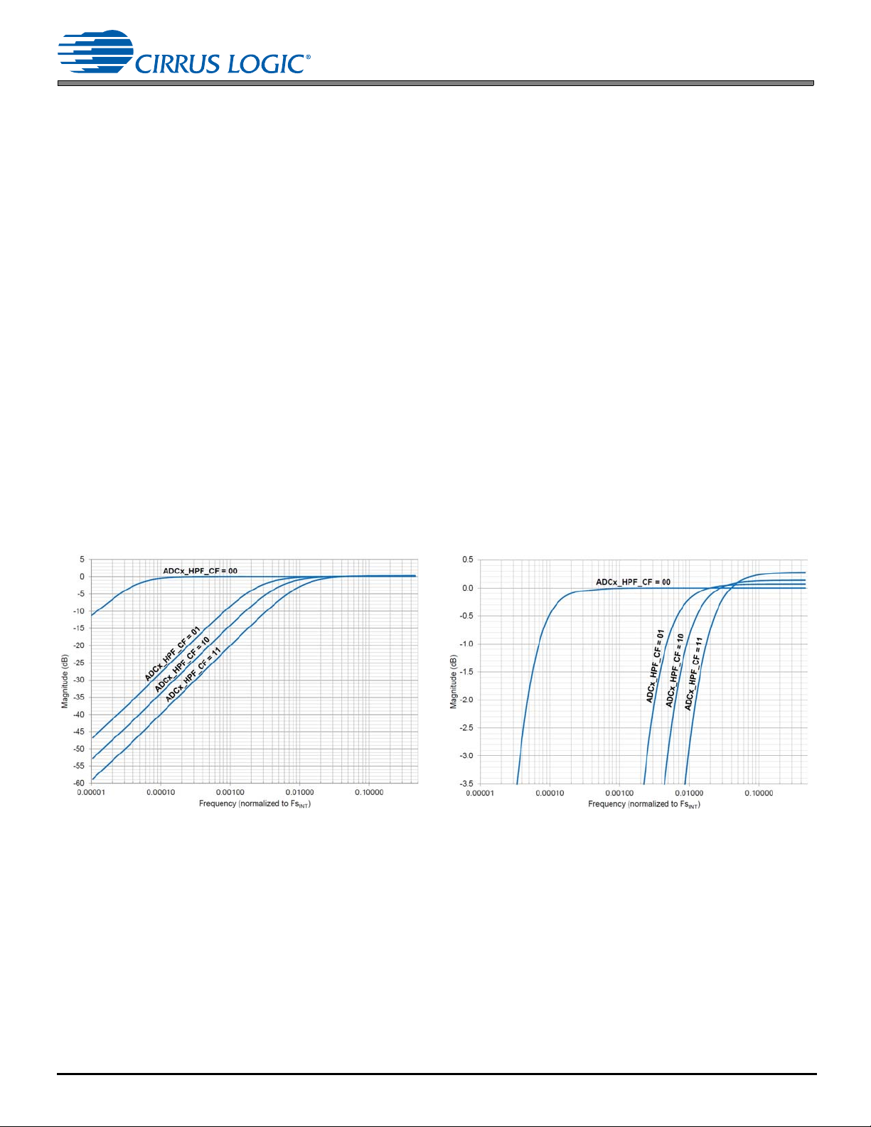
CS53L30
8 Parameter Definitions
8 Parameter Definitions
Dynamic range. The ratio of the rms value of the signal to the rms sum of all other spectral components over the
specified bandwidth. Dynamic range is a signal-to-noise ratio measurement over the specified band width made
with a –60 dB signal.
Frequency response. A measure of the amplitude response variation from 10 Hz to 20 kHz relative to the amplitude
response at 1 kHz. Frequency response is expressed in decibel units.
Gain drift. The change in gain value with temperature, expressed in ppm/°C units.
Interchannel gain mismatch. The gain difference between left and right channe l pairs. Inte rchannel gain m ismatch
is expressed in decibel units.
Interchannel isolation. A measure of crosstalk between the left- and right-channel pairs. Interchannel Isolation is
measured for each channel at the converter's output with no signal to the input under test and a full-scale signal
applied to the other channel. Interchannel isolation is expressed in decibel units.
Load resistance and capacitance. The recommended minimum resistance an d maximum capacitance required for
the internal op-amp's stability and signal integrity. The load capacitance effectively moves the band-limiting pole
of the amp in the output stage. Increasing th e load ca pa cit an ce bey on d th e re co mm e nd e d value can ca us e the
internal op-amp to become unstable.
9Plots
9.1 Digital Filter Response
9.1.1 ADC High-Pass Filter
Figure 9-1. ADC HPF Response Figure 9-2. ADC HPF Response, Passband Detail
58 DS992F1
Page 59

CS53L30
0 0.05 0.1
0.15 0.2 0.25 0.3
0.35 0. 4 0.45 0. 5
-0.25
-0.2
-0.15
-0.1
-0.05
0
0.05
0.1
0.15
0.2
0.25
Frequency (Normal ized t o Fs)
Magnitude (dB )
0 0. 5 1
1.5 2 2. 5 3
-100
-90
-80
-70
-60
-50
-40
-30
-20
-10
0
Frequency (norm alized t o Fs)
Magnitude (dB )
0.3 0.35 0. 4 0. 45 0.5
0.55 0.6 0. 65 0. 7
-100
-90
-80
-70
-60
-50
-40
-30
-20
-10
0
Frequency (Normal ized t o Fs)
Magnitude (dB )
0
0.05 0. 1
0.15 0. 2
0.25 0. 3
0.35 0. 4
0.45 0. 5
-700
-600
-500
-400
-300
-200
-100
0
Frequency (normal ized to Fs)
Phase (degrees)
0 0.05 0.1
0.15 0.2 0.25 0.3 0.35
0.4 0. 45 0.5
-0.25
-0.2
-0.15
-0.1
-0.05
0
0.05
0.1
0.15
0.2
0.25
Frequency (norm alized t o Fs)
Magnitude (dB )
0 0. 5
1 1.5 2 2.5 3
-100
-90
-80
-70
-60
-50
-40
-30
-20
-10
0
Frequency (norm alized t o Fs)
Magnitude (dB )
9.1 Digital Filter Response
9.1.2 Combined ADC and SRC Response, Fs
Figure 9-3. Passband—ADCx, Notch Enabled Figure 9-4. Stopband—ADCx, Notch Enab led
ext
= Fs
int
Figure 9-5. Transition Band—ADCx, Notch Enabled Figure 9-6. Phase Response—ADCx, Notch Enabled
DS992F1 59
Figure 9-7. Passband—ADCx, Notch Disabled Figure 9-8. Stopband—ADCx, Notch Disabled
Page 60

CS53L30
0.3 0.35 0. 4 0. 45 0.5
0.55 0.6 0. 65 0. 7
-100
-90
-80
-70
-60
-50
-40
-30
-20
-10
0
Frequency (norm alized t o Fs)
Magnitude (dB )
0 0.05
0.1 0.15
0.2 0.25
0.3 0.35
0.4 0.45
0.5
-600
-500
-400
-300
-200
-100
0
Frequency (normal ized to Fs)
Phase (degrees)
0 0.05 0.1
0.15 0.2 0.25 0.3
0.35 0. 4 0.45 0. 5
-0.25
-0.2
-0.15
-0.1
-0.05
0
0.05
0.1
0.15
0.2
0.25
Frequency (norm alized t o Fs
ext
)
Magnitude (dB )
0 0. 5 1 1.5 2
2.5 3
-160
-140
-120
-100
-80
-60
-40
-20
0
Frequency (norm alized t o Fs
ext
)
Magnitude (dB )
0.4 0. 42 0.44 0.46 0.48
0.5 0. 52 0.54 0.56
0.58 0. 6
-160
-140
-120
-100
-80
-60
-40
-20
0
Frequency (norm alized t o Fs
ext
)
Magnitude (dB )
0 0.05
0.1 0.15
0.2 0.25
0.3 0.35
0.4 0.45
0.5
-1000
-900
-800
-700
-600
-500
-400
-300
-200
-100
0
Frequency (normal ized to Fs
ext
)
Phase (degrees)
9.1 Digital Filter Response
Figure 9-9. Transition Band—ADCx, Notch Disabled Figure 9-10. Phase Response—ADCx, Notch Disabled
9.1.3 Combined ADC and SRC Response, Fs
Figure 9-11. Passband—ADCx, Notch Enabled Figure 9-12. Stopband—ADCx, Notch Enabled
= 50 kHz, Fs
ext
= 16 kHz, MCLK = 19.2 MHz
int
Figure 9-13. Transition Band—ADCx, Notch Enabled Figure 9-14. Phase Response—ADCx, Notch Enabled
60 DS992F1
Page 61

CS53L30
0 0.05 0.1
0.15 0.2 0.25 0.3
0.35 0. 4 0.45 0. 5
-0.25
-0.2
-0.15
-0.1
-0.05
0
0.05
0.1
0.15
0.2
0.25
Frequency (norm alized t o Fs
ext
)
Magnitude (dB )
0 0. 5 1 1.5 2
2.5 3
-160
-140
-120
-100
-80
-60
-40
-20
0
Frequency (norm alized t o Fs
ext
)
Magnitude (dB )
0.4
0.42 0. 44
0.46 0. 48
0.5 0. 52
0.54 0.56
0.58 0. 6
-160
-140
-120
-100
-80
-60
-40
-20
0
Frequency (norm alized t o Fs
ext
)
Magnitude (dB )
0 0.05
0.1 0.15
0.2 0.25
0.3 0.35
0.4 0.45
0.5
-1000
-900
-800
-700
-600
-500
-400
-300
-200
-100
0
Frequency (normal ized to Fs
ext
)
Phase (degrees)
0 0.05 0.1
0.15 0.2 0.25 0.3 0.35
0.4 0. 45 0.5
-0.25
-0.2
-0.15
-0.1
-0.05
0
0.05
0.1
0.15
0.2
0.25
Frequency (norm alized t o Fs)
Magnitude (dB )
0 0. 5 1
1.5 2 2. 5 3
-100
-90
-80
-70
-60
-50
-40
-30
-20
-10
0
Frequency (norm alized t o Fs)
Magnitude (dB )
9.1 Digital Filter Response
Figure 9-15. Passband—ADCx, Notch Disabled Figure 9-16. Stopband—ADCx, Notch Disabled
Figure 9-17. Transition Band—ADCx, Notch Disabled Figure 9-18. Phase Response—ADCx, Notch Disabled
9.1.4 Combined DMIC and SRC Response, Fs
DS992F1 61
Figure 9-19. Passband—DMICx, Notch Disabled Figure 9-20. Stopband—DMICx, Notch Disabled
= Fs
ext
int
Page 62

9.2 PGA Gain Linearity
0.3 0.35 0. 4 0. 45 0.5
0.55 0.6 0. 65 0. 7
-100
-90
-80
-70
-60
-50
-40
-30
-20
-10
0
Frequency (norm alized t o Fs)
Magnitude (dB )
0 0.05
0.1 0.15
0.2 0.25
0.3 0.35
0.4 0.45
0.5
-600
-500
-400
-300
-200
-100
0
Frequency (normal ized to Fs)
Phase (degrees)
0.475
0.480
0.485
0.490
0.495
0.500
0.505
0.510
0.515
0.520
0.525
-6.0 -3.0 0.0 3.0 6.0 9.0 12.0
Step Size (dB)
PGA Volume Setting (dB)
-6.0
-4.0
-2.0
0.0
2.0
4.0
6.0
8.0
10.0
12.0
-6.0 -3.0 0.0 3.0 6.0 9.0 12.0
Output Level (dB)
PGA Volume Setting (dB)
Figure 9-21. Transition Band—DMICx, Notch Disabled Figure 9-22. Phase Response—DMICx, Notch Disabled
9.2 PGA Gain Linearity
CS53L30
Figure 9-23. PGA DNL Figure 9-24. PGA INL
62 DS992F1
Page 63

9.3 Dynamic Range Versus Sampling Frequency
90
91
92
93
94
95
96
97
98
99
100
8kHz 11.025kHz 12kHz 16kHz 22.05kHz 24kHz 32kHz 44.1kHz 48kHz
DynamicRange(dB,AͲweighted)
SamplingFrequency(Fs
ext
)
MCLK_INT_SCALE=0
MCLK_INT_SCALE=1
G
%
)
6
N N N N N
+]
G
%
)
6
N N N N N
+]
Figure 9-25. Dynamic Range Versus Sampling Frequency
9.4 FFTs
CS53L30
9.3 Dynamic Range Versus Sampling Frequency
Figure 9-26. FFT, 1 kHz, –1 dBFS, Preamp Setting: 0 dB
PGA Setting: 0 dB, Fs
DS992F1 63
= Fs
int
= 48 kHz
ext
Figure 9-27. FFT, 1 kHz, –1 dBFS, Preamp Setting: 0 dB,
PGA Setting: +12 dB, Fs
int
= Fs
= 48 kHz
ext
Page 64

CS53L30
G
%
)
6
N N N N N
+]
G
%
)
6
N N N N N
+]
G
%
)
6
N N N N N
+]
G
%
)
6
N N N N N
+]
G
%
)
6
N N N N N
+]
9.4 FFTs
Figure 9-28. FFT, 1 kHz, –1 dBFS, Preamp Setting: +10 dB,
PGA Setting: 0 dB, Fs
int
= Fs
= 48 kHz
ext
Figure 9-30. FFT, 1 kHz, –1 dBFS, Preamp Setting: +20 dB,
PGA Setting: 0 dB, Fs
int
= Fs
= 48 kHz
ext
Figure 9-29. FFT, 1 kHz, –1 dBFS, Preamp Setting: +10 dB,
PGA Setting: +12 dB, Fs
int
= Fs
= 48 kHz
ext
Figure 9-31. FFT, 1 kHz, –1 dBFS, Preamp Setting: +20 dB,
PGA Setting: +12 dB, Fs
int
= Fs
= 48 kHz
ext
64 DS992F1
Figure 9-32. FFT, No Input, Preamp Setting: 0 dB,
PGA Setting: 0 dB, Fs
int
= Fs
= 48 kHz
ext
Page 65

10Package Dimensions
WAFER BACK SI DE SIDE VI EW BUMP SIDE
e
N
Y
A
A2
A1
M
X
c
d
Ball A1
Ball A 1
Location
Indicator
b
eSeating plane
Ball A1 location indicator
(seen through package)
Z
X
X
øb
Øddd Z X Y
Øccc Z
Notes:
• Dimensioning and tolerances per ASME Y 14.5M–1994.
• The Ball A1 position indicator is for illustration purposes only and may not be to scale.
• Dimension “b” applies to the solder sphere diameter and is measured at the mid point between the package body and th e seating plane
datum Z.
10.1 WLCSP Package
CS53L30
10 Package Dimensions
ccc = 0.05
ddd = 0.15
Figure 10-1. 30-Ball WLCSP Package Drawing
Table 10-1. WLCSP Package Dimensions
Dim
Dimensions (Millimeters)
Min Nom Max
A 0.450 0.505 0.560
A1 0.170 0.200 0.230
A2 0.280 0.305 0.330
M BSC 2.000 BSC
N BSC 1.600 BSC
b 0.230 0.260 0.290
c REF 0.306 REF
d REF 0.306 REF
e BSC 0.400 BSC
X 2.593 2.613 2.633
Y 2.193 2.213 2.233
DS992F1 65
Page 66

10.2 QFN Package
b
A
A1
Pin #1 Corner
E
D2
Pin #1 Cor ner
E2
D
Top View Side View Bottom View
e
L
CS53L30
10.2 QFN Package
Figure 10-2. 32-Pin QFN Package Drawing
Dim
Min Nom Max
Millimeters
1
A— —1.00
A1 0.00 — 0.05
b 0.200.250.30
D 5.00 BSC
D2 3.55 3.65 3.75
E 5.00 BSC
E2 3.55 3.65 3.75
e 0.50 BSC
L 0.350.400.45
JEDEC #: MO–220
Controlling dimension is millimeters.
1. Dimensioning and tolerances per ASME Y 14.5M–1995.
2. Dimensioning lead width applies to the plated terminal an d is measured between 0.2 0 and 0.25 mm from
the terminal tip.
11Thermal Characteristics
Table 11-1. Thermal Characteristics
Parameters
Junction-to-ambient thermal impedance WLCSP
Junction-to-printed circuit board thermal impedanc e WLCSP
1.Test printed circuit board assembly (PCBA) constructed in accordance with JEDEC standard JESD51–9. Two-signal, two-plane (2s2p) PCB used.
2.Test conducted with still air on a four-layer board in accordance with JEDEC standards, JESD51, JESD51–2A, and JESD51–8.
1,2
QFN
QFN
Symbol Min Typ Max Units
JA
JB
—
—
—
—
61
28
10
15
—
—
—
—
°C/W
°C/W
°C/W
°C/W
12Ordering Information
Table 12-1. Ordering Information
Product Description Package Pb Free Grade Temp Range Container Order #
CS53L30 Low-Power Quad-Channel
Microphone ADC with TDM Output
66 DS992F1
30-ball WLCSP Yes Commercial –10°C to +70°C Tape and reel CS53L30-CWZR
32-pin QFN Yes Commercial –10°C to +70°C Tape and reel CS53L30-CNZR
Rail CS53L30-CNZ
Page 67

13Revision History
Contacting Cirrus Logic Support
For all product questions and inquiries, contact a Cirrus Logic Sales Representative.
To find one nearest you, go to www.cirrus.com.
IMPORTANT NOTICE
Cirrus Logic, Inc. and its subsidiaries (“Cirrus”) believe that the information contained in this document is accurate and reliable. However, the information is subject to change
without notice and is provided “AS IS” without warranty of any kind (express or implied). Customers are advised to obta in the latest versio n of re l evan t in f ormat i o n to ver i f y,
before placing orders, that information being relied on is current and complete. All products are sold subject to the terms and co nditions of sale supplied at the time of order
acknowledgment, including those pertaining to warranty, indemnification, and limitation of liability. No responsibility is assumed by Cirrus for the use of this informat ion, including use of this information as the basis for manufacture or sale of any items, or for infringement of patents or other rights of third parties. This docu ment i s the property
of Cirrus and by furnishing this information, Cirrus grants no license, express or implied u nder any patents, mask work rights, copyrights, trademarks, trade secrets or other
intellectual propert y rig hts. Cirrus owns th e copyri ght s asso ciat ed with the inf ormat ion con tain ed her ein and gi ves consent for copies to be made of the information only for
use within your organization with respect to Cirrus integrated circuits or other products of Cirrus. This consent does not extend to other copying such as copying for general
distribution, advertising or promotional pu rposes, or for creating any work for resale.
CERTAIN APPLICATIONS USING SEMICONDUCTOR PRODUCTS MAY INVOLVE POTENTIAL RISKS OF DEATH, PERSONAL INJURY, OR SEVERE PROPERTY OR
ENVIRONMENTAL DAMAGE (“CRITICAL APPLI CATIONS”). CIRRUS PRODUCTS ARE NOT DESIGNED, AUTHORIZED OR WARRANTED FOR USE IN PRODUCTS
SURGICALLY IMPLANTED INTO THE BODY, AUTOMOTIVE SAFETY OR SECURITY DEVICES, LIFE SUPPORT PRODUCTS OR OTHER CRITICAL APPLICATIONS.
INCLUSION OF CIRRUS PRODUCTS IN SUCH APPLICATIONS IS UNDERSTOOD TO BE FULLY AT THE CUSTOMER’S RISK AND CIRRUS DISCLAIMS AND MAKES
NO WARRANTY, EXPRESS, STATUTORY OR I MPLIED, INCLUDING THE IMPLIED WARRANTIES OF MERCHANTABILITY AND FITNESS FOR PARTICULAR PURPOSE, WITH REGARD TO ANY CIRRUS PRODUCT THAT IS USED IN SUCH A MANNER. IF THE CUSTOMER OR CUSTOMER’S CUSTOMER USES OR PERMITS
THE USE OF CIRRUS PRODUCTS IN CRITICAL APPLICATIONS, CUSTOMER AGREES, BY SUCH USE, TO FULLY INDEMNIFY CIRRUS, ITS OFFICERS, DIRECTORS, EMPLOYEES, DISTRIBUTORS AND OTHER AGEN TS FROM ANY AND ALL LIABILITY, I NCLUDING ATTORNEYS’ FEES AND COSTS, THAT MAY RESULT
FROM OR ARISE IN CONNECTION WITH THESE USES.
Cirrus Logic, Cirrus, and the Cirrus Logic logo designs are trademarks of Cirrus Logic, Inc. All other brand and product names in this document may be trademarks or service
marks of their respective owners.
Bluetooth is a registered trademark of the Bluetoo th Special Interest Group (SIG).
I2C is a trademark of Philips Semiconductor.
Revision Change
F1 • Provided specific range of audio sample rates in System Features section on p. 1.
• Added
• Added reference to Section 5.7 in Note 8 in Fig. 2-2.
• Updated mic bias startup delay specification in Table 3-6.
• Added power consumption register field settings in Table3-9.
• Updated maximum SCLK duty cycle specification for I
• Updated min and max specifications for t
• Updated figure in Note 8 in Table 3-12.
• Clarified that ADC1x_PDN and ADC2x_PDN bits must be set when inpu t channel type is digital in Section 7.23 and
• Reformatted presentation of WLCSP pa ckage dimensions in Section 10.1.
Note 6 to Fig. 2-1 and Fig. 2-2.
Section 7.29.
2
S master mode in Table 3-11.
when SHIFT_LEFT = 1 in Table 3-12.
HOLD2
CS53L30
13 Revision History
DS992F1 67
 Loading...