

Page 1
CS5376A
Low-power, Multi-channel Decimation Filter
Features
z 1- to 4-channel Digital Decimation Filter
Multiple On-chip FIR and IIR Coefficient Sets
Programmable Coefficients for Custom Filters
Synchronous Operation
z Selectable Output Word Rate
4000, 2000, 1000, 500, 333, 250 SPS
200, 125, 100, 50, 40, 25, 20, 10, 5, 1 SPS
z Digital Gain and Offset Corrections
z Test DAC Bit-stream Generator
Digital Sine Wave Output
z Time Break Controller, General Purpose I/O
z Secondary SPI™ Port, Boundary Scan JTAG
z Microcontroller or EEPROM Configuration
z Small-footprint, 64-pin TQFP Package
z Low Power Consumption
9 mW per Channel at 500 SPS
z Flexible Power Supplies
I/O Interface: 3.3 V or 5.0 V
Digital Logic Core: 3.0 V, 3.3 V or 5.0 V
I
Description
The CS5376A is a multi-function digital filter utilizing a
low-power signal processing architecture to achieve efficient filtering for up to four ∆Σ modulators. By
combining the CS5376A with CS3301A/02A differential
amplifiers, CS5371A/72A ∆Σ modulators, and the
CS4373A ∆Σ test DAC a synchronous, high-resolution,
self-testing, multi-channel me as ur em e nt s yst em can be
designed quickly and easily.
Digital filter coefficients for the CS5376A FIR and IIR filters are included on-chip for a simple setup, or they can
be programmed for custom applications. Selectable digital filter decimation ratios produce output word rates
from 4000 SPS to 1 SPS, resulting in measurement
bandwidths ranging from 1600 Hz down to 400 mHz
when using the on-chip coefficient sets.
The CS5376A includes integrated peripherals to simplify
system design: offset and gain corrections, a test DAC
bit stream generator, a time-break controller, 12 general-purpose I/O pins, a secondary SPI port, and a
boundary scan JTAG port.
ORDERING INFORMATION
See page 106.
http://www.cirrus.com
Se ria l D a ta Ou tp u t P o rt
Decimation and
Filtering Engine
JTAG
Inte rfa c e
TDI
TCK
TRST
TDO
TMS
SDCLK
SDDAT
SDTKI
SDRDY
Modulator Data
Inte rfa c e
MDATA [4:1]
RESET
MFLAG [4:1]
Copyright © Cirrus Logic, Inc. 2008
(All Rights Reserved)
BOOT
Clock and
Synchronization
Serial Peripheral Interface 1
Time Break Controller
Test Bit Stream Controller
General Purpose I/O
Serial Peripheral Interface 2
SPI 1
GPIO
SPI 2
VD (x2)
VDD1
VDD2 (x2)
CLK
SYNC
MCLK
MSYNC
SSI
SCK1
MISO
MOSI
SINT
TIMEB
TBSCLK
TBSDATA
GPIO11:EECS
GPIO10
GPIO9
GPIO8
GPIO7
GPIO6
GPIO5
GPIO4:CS4
GPIO3:CS3
GPIO2:CS2
GPIO1:CS1
GPIO0:CS0
SCK2
SO
SI1
SI2
SI3
SI4
GND1
GND (x2)
GND2 (x2)
SEP ‘08
DS612F4
Page 2

TABLE OF CONTENTS
1. General Description . . . . . . . . . . . . . . . . . . . . . . . . . . . . . . . . . . . . . .7
1.1. Digital Filter Features. . . . . . . . . . . . . . . . . . . . . . . . . . . . . . . . . . . . . . . .7
1.2. Integrated Peripheral Features . . . . . . . . . . . . . . . . . . . . . . . . . . . . . . . .8
1.3. System Level Features . . . . . . . . . . . . . . . . . . . . . . . . . . . . . . . . . . . . . .8
1.4. Configuration Interface. . . . . . . . . . . . . . . . . . . . . . . . . . . . . . . . . . . . . . .9
2. Characteristics and Specifications . . . . . . . . . . . . . . . . . . . . . . . . . 13
Specified Operating Conditions . . . . . . . . . . . . . . . . . . . . . . . . . . . . . . . . . . .13
Absolute Maximum Ratings . . . . . . . . . . . . . . . . . . . . . . . . . . . . . . . . . . . . . .13
Thermal Characteristics. . . . . . . . . . . . . . . . . . . . . . . . . . . . . . . . . . . . . . . . .14
Digital Characteristics . . . . . . . . . . . . . . . . . . . . . . . . . . . . . . . . . . . . . . . . . .14
Power Consumption. . . . . . . . . . . . . . . . . . . . . . . . . . . . . . . . . . . . . . . . . . . .14
Switching Characteristics. . . . . . . . . . . . . . . . . . . . . . . . . . . . . . . . . . . . . . . .15
3. System Design with CS5376A . . . . . . . . . . . . . . . . . . . . . . . . . . . . . 19
3.1. Power Supplies . . . . . . . . . . . . . . . . . . . . . . . . . . . . . . . . . . . . . . . . . . .19
3.2. Reset Control. . . . . . . . . . . . . . . . . . . . . . . . . . . . . . . . . . . . . . . . . . . . .19
3.3. Clock Generation . . . . . . . . . . . . . . . . . . . . . . . . . . . . . . . . . . . . . . . . . .20
3.4. Synchronization . . . . . . . . . . . . . . . . . . . . . . . . . . . . . . . . . . . . . . . . . . .20
3.5. System Configuration. . . . . . . . . . . . . . . . . . . . . . . . . . . . . . . . . . . . . . .20
3.6. Digital Filter Operation . . . . . . . . . . . . . . . . . . . . . . . . . . . . . . . . . . . . . .20
3.7. Data Collection . . . . . . . . . . . . . . . . . . . . . . . . . . . . . . . . . . . . . . . . . . . .20
3.8. Integrated peripherals . . . . . . . . . . . . . . . . . . . . . . . . . . . . . . . . . . . . . .20
4. Power Supplies . . . . . . . . . . . . . . . . . . . . . . . . . . . . . . . . . . . . . . . . .21
4.1. Pin Descriptions. . . . . . . . . . . . . . . . . . . . . . . . . . . . . . . . . . . . . . . . . . .21
4.2. Bypass Capacitors. . . . . . . . . . . . . . . . . . . . . . . . . . . . . . . . . . . . . . . . .22
4.3. Power Consumption . . . . . . . . . . . . . . . . . . . . . . . . . . . . . . . . . . . . . . . .22
5. Reset Control. . . . . . . . . . . . . . . . . . . . . . . . . . . . . . . . . . . . . . . . . . .23
5.1. Pin Descriptions. . . . . . . . . . . . . . . . . . . . . . . . . . . . . . . . . . . . . . . . . . .23
5.2. Reset Self-Tests. . . . . . . . . . . . . . . . . . . . . . . . . . . . . . . . . . . . . . . . . . .23
5.3. Boot Configurations . . . . . . . . . . . . . . . . . . . . . . . . . . . . . . . . . . . . . . . .23
6. Clock Generation. . . . . . . . . . . . . . . . . . . . . . . . . . . . . . . . . . . . . . . . 24
6.1. Pin Description. . . . . . . . . . . . . . . . . . . . . . . . . . . . . . . . . . . . . . . . . . . .24
6.2. Synchronous Clocking . . . . . . . . . . . . . . . . . . . . . . . . . . . . . . . . . . . . . .24
6.3. Master Clock Jitter and Skew. . . . . . . . . . . . . . . . . . . . . . . . . . . . . . . . .24
7. Synchronization. . . . . . . . . . . . . . . . . . . . . . . . . . . . . . . . . . . . . . . . . 25
7.1. Pin Description. . . . . . . . . . . . . . . . . . . . . . . . . . . . . . . . . . . . . . . . . . . .25
7.2. MSYNC Generation . . . . . . . . . . . . . . . . . . . . . . . . . . . . . . . . . . . . . . . .25
7.3. Digital Filter Synchronization . . . . . . . . . . . . . . . . . . . . . . . . . . . . . . . . .25
7.4. Modulator Synchronization . . . . . . . . . . . . . . . . . . . . . . . . . . . . . . . . . .25
7.5. Test Bit Stream Synchronization . . . . . . . . . . . . . . . . . . . . . . . . . . . . . .25
8. Configuration By EEPROM. . . . . . . . . . . . . . . . . . . . . . . . . . . . . . . . 26
8.1. Pin Descriptions. . . . . . . . . . . . . . . . . . . . . . . . . . . . . . . . . . . . . . . . . . .26
8.2. EEPROM Hardware Interface . . . . . . . . . . . . . . . . . . . . . . . . . . . . . . . .26
8.3. EEPROM Organization . . . . . . . . . . . . . . . . . . . . . . . . . . . . . . . . . . . . .26
8.4. EEPROM Configuration Commands . . . . . . . . . . . . . . . . . . . . . . . . . . .28
8.5. Example EEPROM Configuration . . . . . . . . . . . . . . . . . . . . . . . . . . . . .30
9. Configuration By Microcontroller . . . . . . . . . . . . . . . . . . . . . . . . . . 32
CS5376A
DS612F4 2
Page 3

9.1. Pin Descriptions. . . . . . . . . . . . . . . . . . . . . . . . . . . . . . . . . . . . . . . . . . .32
9.2. Microcontroller Hardware Interface . . . . . . . . . . . . . . . . . . . . . . . . . . . .32
9.3. Microcontroller Serial Transactions . . . . . . . . . . . . . . . . . . . . . . . . . . . .32
9.4. Microcontroller Configuration Commands . . . . . . . . . . . . . . . . . . . . . . .35
9.5. Example Microcontroller Configuration . . . . . . . . . . . . . . . . . . . . . . . . .37
10. Modulator Interface. . . . . . . . . . . . . . . . . . . . . . . . . . . . . . . . . . . . . 39
10.1. Pin Descriptions. . . . . . . . . . . . . . . . . . . . . . . . . . . . . . . . . . . . . . . . . .39
10.2. Modulator Clock Generation . . . . . . . . . . . . . . . . . . . . . . . . . . . . . . . .39
10.3. Modulator Synchronization. . . . . . . . . . . . . . . . . . . . . . . . . . . . . . . . . .39
10.4. Modulator Data Inputs . . . . . . . . . . . . . . . . . . . . . . . . . . . . . . . . . . . . .40
10.5. Modulator Flag Inputs . . . . . . . . . . . . . . . . . . . . . . . . . . . . . . . . . . . . .40
11. Digital Filter Initialization . . . . . . . . . . . . . . . . . . . . . . . . . . . . . . . . 41
11.1. Filter Coefficient Selection . . . . . . . . . . . . . . . . . . . . . . . . . . . . . . . . . .41
11.2. Filter Configuration Options . . . . . . . . . . . . . . . . . . . . . . . . . . . . . . . . .41
12. SINC Filter . . . . . . . . . . . . . . . . . . . . . . . . . . . . . . . . . . . . . . . . . . . . 43
12.1. SINC1 Filter . . . . . . . . . . . . . . . . . . . . . . . . . . . . . . . . . . . . . . . . . . . . .43
12.2. SINC2 Filter . . . . . . . . . . . . . . . . . . . . . . . . . . . . . . . . . . . . . . . . . . . . .43
12.3. SINC3 Filter . . . . . . . . . . . . . . . . . . . . . . . . . . . . . . . . . . . . . . . . . . . . .43
12.4. SINC Filter Synchronization. . . . . . . . . . . . . . . . . . . . . . . . . . . . . . . . .43
13. FIR Filter. . . . . . . . . . . . . . . . . . . . . . . . . . . . . . . . . . . . . . . . . . . . . . 47
13.1. FIR1 Filter . . . . . . . . . . . . . . . . . . . . . . . . . . . . . . . . . . . . . . . . . . . . . .47
13.2. FIR2 Filter . . . . . . . . . . . . . . . . . . . . . . . . . . . . . . . . . . . . . . . . . . . . . .47
13.3. On-Chip FIR Coefficients. . . . . . . . . . . . . . . . . . . . . . . . . . . . . . . . . . .47
13.4. Programmable FIR Coefficients. . . . . . . . . . . . . . . . . . . . . . . . . . . . . .48
13.5. FIR Filter Synchronization . . . . . . . . . . . . . . . . . . . . . . . . . . . . . . . . . .48
14. IIR Filter . . . . . . . . . . . . . . . . . . . . . . . . . . . . . . . . . . . . . . . . . . . . . . 55
14.1. IIR Architecture . . . . . . . . . . . . . . . . . . . . . . . . . . . . . . . . . . . . . . . . . .55
14.2. IIR1 Filter . . . . . . . . . . . . . . . . . . . . . . . . . . . . . . . . . . . . . . . . . . . . . . .55
14.3. IIR2 Filter . . . . . . . . . . . . . . . . . . . . . . . . . . . . . . . . . . . . . . . . . . . . . . .55
14.4. IIR3 Filter . . . . . . . . . . . . . . . . . . . . . . . . . . . . . . . . . . . . . . . . . . . . . . .56
14.5. On-Chip IIR Coefficients . . . . . . . . . . . . . . . . . . . . . . . . . . . . . . . . . . .56
14.6. Programmable IIR Coefficients . . . . . . . . . . . . . . . . . . . . . . . . . . . . . .56
14.7. IIR Filter Synchronization. . . . . . . . . . . . . . . . . . . . . . . . . . . . . . . . . . .56
15. Gain and Offset Correction. . . . . . . . . . . . . . . . . . . . . . . . . . . . . . . 59
15.1. Gain Correction . . . . . . . . . . . . . . . . . . . . . . . . . . . . . . . . . . . . . . . . . .59
15.2. Offset Correction . . . . . . . . . . . . . . . . . . . . . . . . . . . . . . . . . . . . . . . . .59
15.3. Offset Calibration . . . . . . . . . . . . . . . . . . . . . . . . . . . . . . . . . . . . . . . . .60
16. Serial Data Port . . . . . . . . . . . . . . . . . . . . . . . . . . . . . . . . . . . . . . . . 61
16.1. Pin Descriptions. . . . . . . . . . . . . . . . . . . . . . . . . . . . . . . . . . . . . . . . . .61
16.2. SD Port Data Format . . . . . . . . . . . . . . . . . . . . . . . . . . . . . . . . . . . . . .61
16.3. SD Port Transactions. . . . . . . . . . . . . . . . . . . . . . . . . . . . . . . . . . . . . .62
17. Test Bit Stream Generator . . . . . . . . . . . . . . . . . . . . . . . . . . . . . . .64
17.1. Pin Descriptions. . . . . . . . . . . . . . . . . . . . . . . . . . . . . . . . . . . . . . . . . .64
17.2. TBS Architecture . . . . . . . . . . . . . . . . . . . . . . . . . . . . . . . . . . . . . . . . .64
17.3. TBS Configuration . . . . . . . . . . . . . . . . . . . . . . . . . . . . . . . . . . . . . . . .64
17.4. TBS Data Source. . . . . . . . . . . . . . . . . . . . . . . . . . . . . . . . . . . . . . . . .65
17.5. TBS Sine Wave Output . . . . . . . . . . . . . . . . . . . . . . . . . . . . . . . . . . . .66
17.6. TBS Loopback Testing. . . . . . . . . . . . . . . . . . . . . . . . . . . . . . . . . . . . .66
CS5376A
DS612F4 3
Page 4

17.7. TBS Synchronization . . . . . . . . . . . . . . . . . . . . . . . . . . . . . . . . . . . . . .66
18. Time Break Controller. . . . . . . . . . . . . . . . . . . . . . . . . . . . . . . . . . .67
18.1. Pin Description. . . . . . . . . . . . . . . . . . . . . . . . . . . . . . . . . . . . . . . . . . .67
18.2. Time Break Operation . . . . . . . . . . . . . . . . . . . . . . . . . . . . . . . . . . . . .67
18.3. Time Break Delay. . . . . . . . . . . . . . . . . . . . . . . . . . . . . . . . . . . . . . . . .67
19. General Purpose I/O . . . . . . . . . . . . . . . . . . . . . . . . . . . . . . . . . . . . 68
19.1. Pin Descriptions. . . . . . . . . . . . . . . . . . . . . . . . . . . . . . . . . . . . . . . . . .68
19.2. GPIO Architecture . . . . . . . . . . . . . . . . . . . . . . . . . . . . . . . . . . . . . . . .68
19.3. GPIO Registers . . . . . . . . . . . . . . . . . . . . . . . . . . . . . . . . . . . . . . . . . .68
19.4. GPIO Input Mode. . . . . . . . . . . . . . . . . . . . . . . . . . . . . . . . . . . . . . . . .68
19.5. GPIO Output Mode . . . . . . . . . . . . . . . . . . . . . . . . . . . . . . . . . . . . . . .68
20. Serial Peripheral Interface 2. . . . . . . . . . . . . . . . . . . . . . . . . . . . . . 70
20.1. Pin Descriptions. . . . . . . . . . . . . . . . . . . . . . . . . . . . . . . . . . . . . . . . . .70
20.2. SPI 2 Architecture . . . . . . . . . . . . . . . . . . . . . . . . . . . . . . . . . . . . . . . .70
20.3. SPI 2 Registers . . . . . . . . . . . . . . . . . . . . . . . . . . . . . . . . . . . . . . . . . .70
20.4. SPI 2 Transactions. . . . . . . . . . . . . . . . . . . . . . . . . . . . . . . . . . . . . . . .72
21. Boundary Scan JTAG . . . . . . . . . . . . . . . . . . . . . . . . . . . . . . . . . . . 75
21.1. Pin Descriptions. . . . . . . . . . . . . . . . . . . . . . . . . . . . . . . . . . . . . . . . . .75
21.2. JTAG Architecture . . . . . . . . . . . . . . . . . . . . . . . . . . . . . . . . . . . . . . . .75
22. Device Revision History . . . . . . . . . . . . . . . . . . . . . . . . . . . . . . . . . 78
22.1. Changes from CS5376 rev A to CS5376 rev B . . . . . . . . . . . . . . . . . .78
22.2. Changes from CS5376 rev B to CS5376A rev A. . . . . . . . . . . . . . . . .78
23. Register Summary. . . . . . . . . . . . . . . . . . . . . . . . . . . . . . . . . . . . . . 81
23.1. SPI 1 Registers . . . . . . . . . . . . . . . . . . . . . . . . . . . . . . . . . . . . . . . . . .81
23.2. Digital Filter Registers . . . . . . . . . . . . . . . . . . . . . . . . . . . . . . . . . . . . .86
24. Pin Descriptions . . . . . . . . . . . . . . . . . . . . . . . . . . . . . . . . . . . . . . 102
25. Package Dimensions. . . . . . . . . . . . . . . . . . . . . . . . . . . . . . . . . . . 105
26. Ordering Information . . . . . . . . . . . . . . . . . . . . . . . . . . . . . . . . . .106
27. Environmental, Manufacturing, & Handling Information. . . . . . 106
28. Revision History . . . . . . . . . . . . . . . . . . . . . . . . . . . . . . . . . . . . . . 106
CS5376A
LIST OF FIGURES
Figure 1. CS5376A Block Diagram. . . . . . . . . . . . . . . . . . . . . . . . . . . . . . . . . . . .7
Figure 2. Digital Filtering Stages. . . . . . . . . . . . . . . . . . . . . . . . . . . . . . . . . . . . . .8
Figure 3. FIR and IIR Coefficient Set Selection Word. . . . . . . . . . . . . . . . . . . . .11
Figure 4. MOSI Write Timing in SPI Slave Mode . . . . . . . . . . . . . . . . . . . . . . . .15
Figure 5. MISO Read Timing in SPI Slave Mode . . . . . . . . . . . . . . . . . . . . . . . .15
Figure 6. SD Port Read Timing. . . . . . . . . . . . . . . . . . . . . . . . . . . . . . . . . . . . . .16
Figure 7. SYNC, MCLK, MSYNC, MDATA Interface Timing . . . . . . . . . . . . . . .17
Figure 8. TBS Output Clock and Data Timing. . . . . . . . . . . . . . . . . . . . . . . . . . .18
Figure 9. Multi-Channel System Block Diagram. . . . . . . . . . . . . . . . . . . . . . . . .19
Figure 10. Power Supply Block Diagram . . . . . . . . . . . . . . . . . . . . . . . . . . . . . .21
Figure 11. Reset Control Block Diagram . . . . . . . . . . . . . . . . . . . . . . . . . . . . . .23
Figure 12. Clock Generation Block Diagram. . . . . . . . . . . . . . . . . . . . . . . . . . . .24
Figure 13. Synchronization Block Diagram. . . . . . . . . . . . . . . . . . . . . . . . . . . . .25
DS612F4 4
Page 5

Figure 14. EEPROM Configuration Block Diagram . . . . . . . . . . . . . . . . . . . . . .26
Figure 15. SPI 1 EEPROM Read Transactions . . . . . . . . . . . . . . . . . . . . . . . . .27
Figure 16. 8 Kbyte EEPROM Memory Organization. . . . . . . . . . . . . . . . . . . . . .28
Figure 17. Serial Peripheral Interface 1 (SPI 1) Block Diagram . . . . . . . . . . . . .32
Figure 18. Microcontroller Serial Transactions . . . . . . . . . . . . . . . . . . . . . . . . . .33
Figure 19. SPI 1 Registers . . . . . . . . . . . . . . . . . . . . . . . . . . . . . . . . . . . . . . . . .34
Figure 20. Modulator Data Interface. . . . . . . . . . . . . . . . . . . . . . . . . . . . . . . . . .39
Figure 21. Digital Filter Stages . . . . . . . . . . . . . . . . . . . . . . . . . . . . . . . . . . . . . .41
Figure 22. FIR and IIR Coefficient Set Selection Word. . . . . . . . . . . . . . . . . . . .42
Figure 23. SINC Filter Block Diagram. . . . . . . . . . . . . . . . . . . . . . . . . . . . . . . . .43
Figure 24. SINC Filter Stages. . . . . . . . . . . . . . . . . . . . . . . . . . . . . . . . . . . . . . .44
Figure 25. FIR Filter Block Diagram . . . . . . . . . . . . . . . . . . . . . . . . . . . . . . . . . .47
Figure 26. FIR Filter Stages . . . . . . . . . . . . . . . . . . . . . . . . . . . . . . . . . . . . . . . .49
Figure 27. Minimum Phase Group Delay . . . . . . . . . . . . . . . . . . . . . . . . . . . . . .51
Figure 28. IIR Filter Block Diagram. . . . . . . . . . . . . . . . . . . . . . . . . . . . . . . . . . .55
Figure 29. IIR Filter Stages. . . . . . . . . . . . . . . . . . . . . . . . . . . . . . . . . . . . . . . . .57
Figure 30. Gain and Offset Correction . . . . . . . . . . . . . . . . . . . . . . . . . . . . . . . .59
Figure 31. Serial Data Port Block Diagram. . . . . . . . . . . . . . . . . . . . . . . . . . . . .61
Figure 32. SD Port Data Format. . . . . . . . . . . . . . . . . . . . . . . . . . . . . . . . . . . . .62
Figure 33. SD Port Transaction . . . . . . . . . . . . . . . . . . . . . . . . . . . . . . . . . . . . .63
Figure 34. Test Bit Stream Generator Block Diagram . . . . . . . . . . . . . . . . . . . .64
Figure 35. Time Break Block Diagram . . . . . . . . . . . . . . . . . . . . . . . . . . . . . . . .67
Figure 36. GPIO Bi-directional Structure . . . . . . . . . . . . . . . . . . . . . . . . . . . . . .68
Figure 37. Serial Peripheral Interface 2 (SPI 2) Block Diagram . . . . . . . . . . . . .70
Figure 38. SPI 2 Master Mode Transactions . . . . . . . . . . . . . . . . . . . . . . . . . . .73
Figure 39. SPI 2 Transaction Details . . . . . . . . . . . . . . . . . . . . . . . . . . . . . . . . .74
Figure 40. JTAG Block Diagram. . . . . . . . . . . . . . . . . . . . . . . . . . . . . . . . . . . . .75
Figure 41. SPI 1 Control Register SPI1CTRL. . . . . . . . . . . . . . . . . . . . . . . . . . .82
Figure 42. SPI 1 Command Register SPI1CMD. . . . . . . . . . . . . . . . . . . . . . . . .83
Figure 43. SPI 1 Data Register SPI1DAT1. . . . . . . . . . . . . . . . . . . . . . . . . . . . .84
Figure 44. SPI 1 Data Register SPI1DAT2. . . . . . . . . . . . . . . . . . . . . . . . . . . . .85
Figure 45. Hardware Configuration Register CONFIG . . . . . . . . . . . . . . . . . . . .87
Figure 46. GPIO Configuration Register GPCFG0. . . . . . . . . . . . . . . . . . . . . . . 8 8
Figure 47. GPIO Configuration Register GPCFG1. . . . . . . . . . . . . . . . . . . . . . . 8 9
Figure 48. SPI 2 Control Register SPI2CTRL. . . . . . . . . . . . . . . . . . . . . . . . . . .90
Figure 49. SPI 2 Command Register SPI2CMD. . . . . . . . . . . . . . . . . . . . . . . . .91
Figure 50. SPI 2 Data Register SPI2DAT. . . . . . . . . . . . . . . . . . . . . . . . . . . . . .92
Figure 51. Filter Configuration Register FILTCFG . . . . . . . . . . . . . . . . . . . . . . .93
Figure 52. Gain Correction Register GAIN1 . . . . . . . . . . . . . . . . . . . . . . . . . . . .94
Figure 53. Offset Correction Register OFFSET1 . . . . . . . . . . . . . . . . . . . . . . . .95
Figure 54. Time Break Counter Register TIMEBRK. . . . . . . . . . . . . . . . . . . . . .96
Figure 55. Test Bit Stream Configuration Register TBSCFG . . . . . . . . . . . . . . .97
Figure 56. Test Bit Stream Gain Register TBSGAIN . . . . . . . . . . . . . . . . . . . . .98
Figure 57. User Defined System Register SYSTEM1. . . . . . . . . . . . . . . . . . . . .99
Figure 58. Hardware Version ID Register VERSION . . . . . . . . . . . . . . . . . . . .100
Figure 59. Self Test Result Register SELFTEST . . . . . . . . . . . . . . . . . . . . . . .101
CS5376A
DS612F4 5
Page 6

LIST OF TABLES
Table 1. Microcontroller and EEPROM Configuration Commands. . . . . . . . . . .10
Table 2. TBS Configurations Using On-Chip Data . . . . . . . . . . . . . . . . . . . . . . .11
Table 3. SPI 1 and Digital Filter Registers . . . . . . . . . . . . . . . . . . . . . . . . . . . . .12
Table 4. Maximum EEPROM Configuration . . . . . . . . . . . . . . . . . . . . . . . . . . . .28
Table 5. EEPROM Boot Configuration Commands . . . . . . . . . . . . . . . . . . . . . .29
Table 6. Example EEPROM File. . . . . . . . . . . . . . . . . . . . . . . . . . . . . . . . . . . . .31
Table 7. Microcontroller Boot Configuration Commands . . . . . . . . . . . . . . . . . .35
Table 8. Example Microcontroller Configuration. . . . . . . . . . . . . . . . . . . . . . . . .38
Table 9. SINC Filter Configurations . . . . . . . . . . . . . . . . . . . . . . . . . . . . . . . . . .44
Table 10. SINC1 and SINC2 Filter Coefficients . . . . . . . . . . . . . . . . . . . . . . . . .45
Table 11. SINC3 Filter Coefficients. . . . . . . . . . . . . . . . . . . . . . . . . . . . . . . . . . .46
Table 12. FIR Filter Characteristics . . . . . . . . . . . . . . . . . . . . . . . . . . . . . . . . . .49
Table 13. SINC + FIR Group Delay . . . . . . . . . . . . . . . . . . . . . . . . . . . . . . . . . .50
Table 14. FIR1 Coefficients . . . . . . . . . . . . . . . . . . . . . . . . . . . . . . . . . . . . . . . .52
Table 15. FIR2 Linear Phase Coefficients . . . . . . . . . . . . . . . . . . . . . . . . . . . . .53
Table 16. FIR2 Minimum Phase Coefficients . . . . . . . . . . . . . . . . . . . . . . . . . . .54
Table 17. IIR Filter Characteristics . . . . . . . . . . . . . . . . . . . . . . . . . . . . . . . . . . .57
Table 18. IIR Filter Coefficients. . . . . . . . . . . . . . . . . . . . . . . . . . . . . . . . . . . . . .58
Table 19. TBS Configurations Using On-chip Data . . . . . . . . . . . . . . . . . . . . . .65
Table 20. JTAG Instructions and IDCODE . . . . . . . . . . . . . . . . . . . . . . . . . . . . .76
Table 21. JTAG Scan Cell Mapping . . . . . . . . . . . . . . . . . . . . . . . . . . . . . . . . . .77
CS5376A
DS612F4 6
Page 7
SDCLK
Serial Data Output Port
Decimation and
Filtering Engine
JTAG
Interface
SDDAT
SDTKI
SDRDY
Modulator Data
Interface
RESET
BOOT
Clock and
Synchronization
Serial Peripheral Interface 1
Time Break Controller
Test Bit Stream Controller
General Purpose I/O
Serial Peripheral Interface 2
SPI 1
GPIO
SPI 2
CS5376A
VD (x2)
VDD1
VDD2 (x2)
CLK
SYNC
MCLK
MSYNC
SSI
SCK1
MISO
MOSI
SINT
TIMEB
TBSCLK
TBSDATA
GPIO11:EECS
GPIO10
GPIO9
GPIO8
GPIO7
GPIO6
GPIO5
GPIO4:CS4
GPIO3:CS3
GPIO2:CS2
GPIO1:CS1
GPIO0:CS0
SCK2
SO
SI1
SI2
SI3
SI4
TDI
TCK
TRST
TDO
TMS
MFLAG [4:1]
MDATA [4:1]
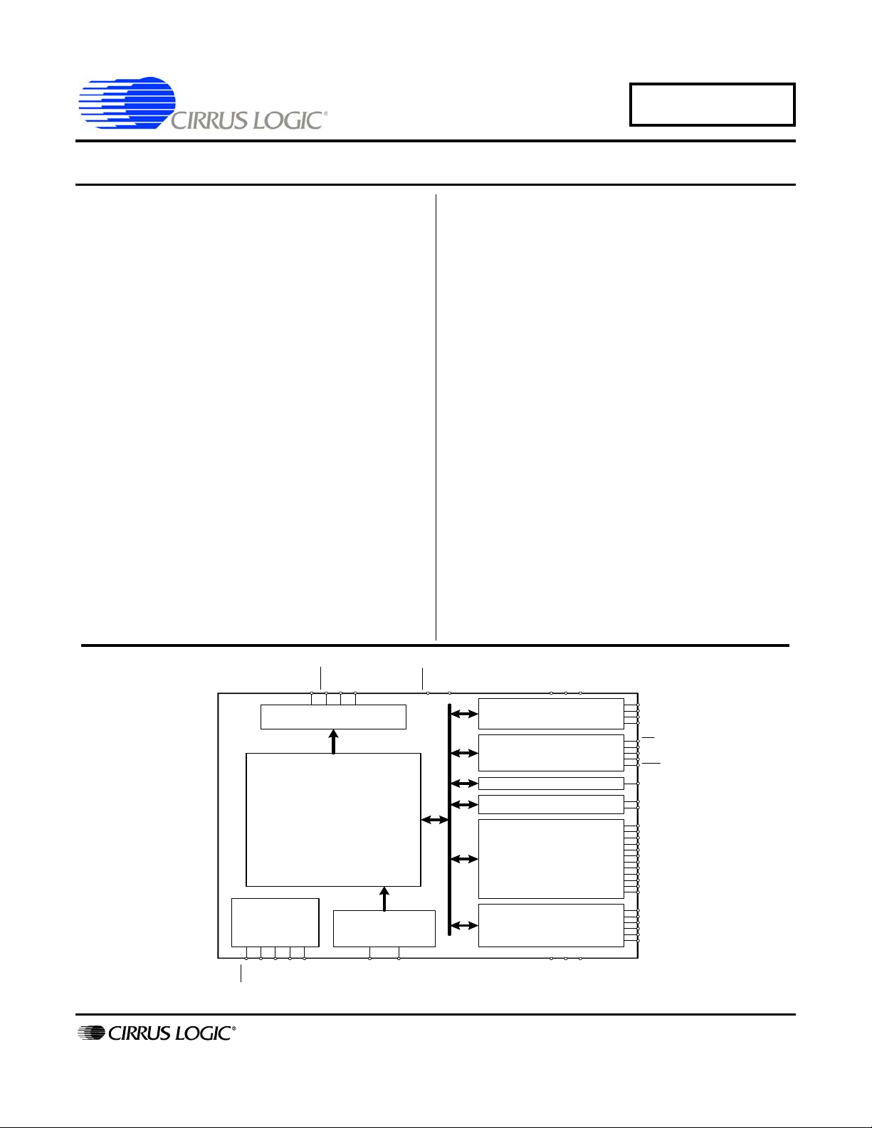
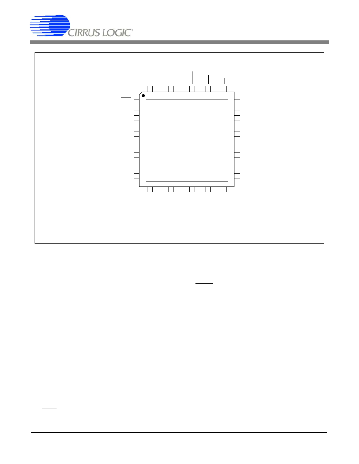
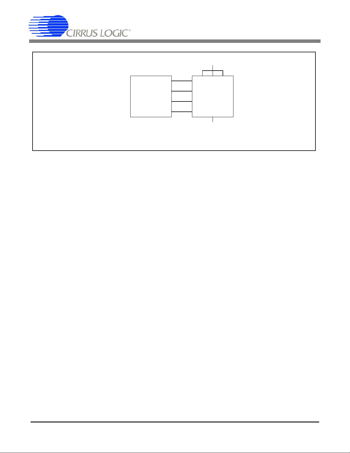
Figure 1. CS5376A Block Diagram
1. GENERAL DESCRIPTION
The CS5376A is a multi-channel digital filter with
integrated system peripherals. Figure 1 illustrates a
simplified block diagram of the CS5376A.
1.1 Digital Filter Features
• Multi-channel decimation filter for
CS5371A/72A ∆Σ modulators.
- 1, 2, 3, or 4 channel concurrent operation.
• Synchronous operation for simultaneous sampling in multi-sensor systems.
- Internal synchronization of digital filter
phase to an external SYNC signal.
• Multiple output word rates, including low
bandwidth rates.
- Standard output rates: 4000, 2000, 1000,
500, 333, 250 SPS.
GND1
GND (x2)
GND2 (x2)
- Low bandwidth rates: 200, 125, 100, 50, 40,
25, 20, 10, 5, 1 SPS.
• Flexible digital filter configuration. (See Figure
2)
- Cascaded SINC, FIR, and IIR filters with
selectable output stage.
- Linear and minimum phase FIR low-pass
filter coefficients included.
- 3 Hz Butterworth IIR high-pass filter coefficients included.
- FIR and IIR coefficients are programmable
to create a custom filter response.
• Digital gain correction.
- Individual channel gain correction to normalize signal amplitudes.
DS612F4 7
Page 8
CS5376A
Modulator
Input
512 kHz
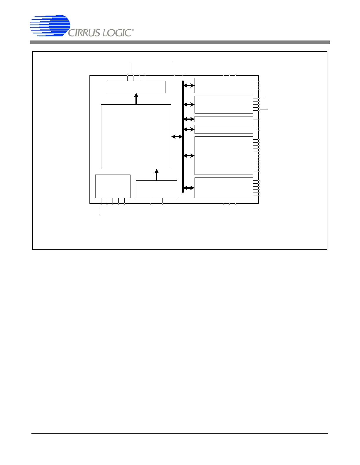
Sinc Filter
2 - 64000
Gain &
DC Offset
Corrections
FIR1
4
Figure 2. Digital Filtering Stages
FIR2
Output Word Rate from 4000 SPS ~ 1 SPS
• Digital offset correction and calibration.
- Individual channel offset correction to remove measurement offsets.
- Calibration engine for automatic calculation of offset correction factors.
1.2 Integrated Peripheral Features
• Synchronous operation for simultaneous sampling in multi-sensor systems.
- MCLK / MSYNC output signals to syn-
chronize external components.
• High speed serial data output port (SD port).
IIR1 IIR2
2
Output to High Speed Serial Data Port
st
1
Order
2nd Order
• Time break controller to record system timing
information.
- Dedicated TB status bit in the output data
stream.
- Programmable output delay to match system group delay.
• Additional hardware peripherals simplify system design.
- 12 General Purpose I/O (GPIO) pins for lo-
cal hardware control.
- Secondary SPI 2 serial port to control local
serial peripherals.
- Asynchronous operation to 4 MHz for direct connection to system telemetry.
- JTAG port for boundary scan (IEEE 1149.1
compliant).
- Internal 8-deep data FIFO for flexible output timing.
• Digital test bit stream signal generator suitable
for CS4373A ∆Σ test DAC.
- Sine wave output mode for testing total har-
monic distortion.
- Programmable waveform data for custom
test signal generation.
8 DS612F4
1.3 System Level Features
• Flexible configuration options.
- Configuration 'on-the-fly' via microcontroller or system telemetry.
- Fixed configuration via stand-alone boot
EEPROM.
• Low power consumption.
Page 9

CS5376A
- 37 mW for 4-channel operation at 500 SPS
(9.25 mW/channel).
-40µW standby mode.
• Flexible power supply configurations.
- Separate digital logic core, telemetry I/O,
and modulator I/O power supplies.
- Telemetry I/O and modulator I/O interfaces
operate from 3.3 V or 5 V.
- Digital logic core operates from 3.0 V,
3.3 V or 5 V.
• Small 64-pin TQFP package.
- Total footprint 12 mm x 12 mm plus five
bypass capacitors.
1.4 Configuration Interface
• Configuration from microcontroller or stand-
alone boot EEPROM.
- Microcontroller boot permits reconfiguration during operation.
- EEPROM boot sets a fixed operational configuration.
• Configuration commands written through Serial Peripheral Interface 1. (See Table 1)
- Standardized microcontroller interface us-
ing SPI 1 registers. (See Table 3)
- Commands write digital filter registers, fil-
ter coefficients, and test bit stream data.
- Digital filter registers set hardware config-
uration options.
DS612F4 9
Page 10
Microcontroller Boot Configuration Commands
CS5376A
Name CMD
24-bit
NOP 000000 - - No Operation
WRITE DF REGISTER 000001 REG DATA Write Digital Filter Register
READ DF REGISTER 000002 REG
WRITE FIR COEFFICIENTS 000003 NUM FIR1
WRITE IIR COEFFICIENTS 000004 a11
WRITE ROM COEFFICIENTS 000005 COEF SEL - Use On-Chip Coefficients
WRITE TBS DATA 000006 NUM TBS
WRITE ROM TBS 000007 - - Use On-Chip TBS Data
FILTER START 000008 - - Start Digital Filter Operation
FILTER STOP 000009 - - Stop Digital Filter Operation
DAT1
24-bit
[DATA]
(FIR COEF)
b11
a22
b21
(TBS DATA)-(TBS DATA)
DAT2
24-bit
-
-
NUM FIR2
(FIR COEF)
b10
a21
b20
b22
Description
Read Digital Filter Register
Write Custom FIR Coefficients
Write Custom IIR Coefficients
Write Custom Test Bit Stream Data
EEPROM Boot Configuration Commands
Name CMD
8-bit
NOP 00 - No Operation
WRITE DF REGISTER 01 REG
WRITE FIR COEFFICIENTS 02 NUM FIR1
WRITE IIR COEFFICIENTS 03 a11
WRITE ROM COEFFICIENTS 04 COEF SEL Use On-Chip Coefficients
WRITE TBS DATA 05 NUM TBS
WRITE ROM TBS 06 - Use On-Chip TBS Data
FILTER START 07 - Start Digital Filter Operation
DATA
24-bit
DATA
NUM FIR2
(FIR COEF)
b10
b11
a21
a22
b20
b21
b22
(TBS DATA)
Description
Write Digital Filter Register
Write Custom FIR Coefficients
Write Custom IIR Coefficients
Write Custom Test Bit Stream Data
[DATA] indicates data word returned from digital filter.
(DATA) indicates multiple words of this type are to be written.
Table 1. Microcontroller and EEPROM Configuration Commands
DS612F4 10
Page 11
CS5376A
Bits 23:20 19:16 15:12 11:8 7:4 3:0
Selection 0000 0000 IIR2 IIR1 FIR2 FIR1
Bits 15:12 IIR2 Coefficients
0000 3 Hz @ 2000 SPS
0001 3 Hz @ 1000 SPS
0010 3 Hz @ 500 SPS
0011 3 Hz @ 333 SPS
0100 3 Hz @ 250 SPS
Figure 3. FIR and IIR Coefficient Set Selection Word
Test Bit Stream Characteristic Equation:
(Signal Freq) * (# TBS Data) * (Interpolation + 1) = Output Rate
Example: (31.25 Hz) * (1024) * (0x07 + 1) = 256 kHz
Signal
Frequency
(TBSDATA)
10.00 Hz 256 kHz 0x4 0x18
10.00 Hz 512 kHz 0x5 0x31
25.00 Hz 256 kHz 0x4 0x09
25.00 Hz 512 kHz 0x5 0x13
31.25 Hz 256 kHz 0x4 0x07
31.25 Hz 512 kHz 0x5 0x0F
50.00 Hz 256 kHz 0x4 0x04
50.00 Hz 512 kHz 0x5 0x09
125.00 Hz 256 kHz 0x4 0x01
125.00 Hz 512 kHz 0x5 0x03
Bits 11:8 IIR1 Coefficients
0000 3 Hz @ 2000 SPS
0001 3 Hz @ 1000 SPS
0010 3 Hz @ 500 SPS
0011 3 Hz @ 333 SPS
0100 3 Hz @ 250 SPS
Output
Output Rate
Rate
(TBSCLK)
Selection
(RATE)
Bits 3:0 FIR1 Coefficients
0000 Linear Phase
0001 Minimum Phase
Bits 7:4 FIR2 Coefficients
0000 Linear Phase
0001 Minimum Phase
Interpolation
Selection
(INTP)
Table 2. TBS Configurations Using On-Chip Data
DS612F4 11
Page 12

SPI 1 Registers
Name Addr. Type # Bits Description
SPI1CTRL 00 - 02 R/W 8, 8, 8 SPI 1 Control
SPI1CMD 03 - 05 R/W 8, 8, 8 SPI 1 Command
SPI1DAT1 06 - 08 R/W 8, 8, 8 SPI 1 Data 1
SPI1DAT2 09 - 0B R/W 8, 8, 8 SPI 1 Data 2
Digital Filter Registers
Name Addr. Type # Bits Description
CONFIG 00 R/W 24 Hardware Configuration
RESERVED 01-0D R/W 24 Reserved
GPCFG0 0E R/W 24 GPIO[7:0] Direction, Pull-up Enable, and Data
GPCFG1 0F R/W 24 GPIO[11:8] Direction, Pull-up Enable, and Data
SPI2CTRL 10 R/W 24 SPI 2 Control
SPI2CMD 11 R/W 16 SPI 2 Command
SPI2DAT 12 R/W 24 SPI 2 Data
RESERVED 13-1F R/W 24 Reserved
FILTCFG 20 R/W 24 Digital Filter Configuration
GAIN1 21 R/W 24 Gain Correction Channel 1
GAIN2 22 R/W 24 Gain Correction Channel 2
GAIN3 23 R/W 24 Gain Correction Channel 3
GAIN4 24 R/W 24 Gain Correction Channel 4
OFFSET1 25 R/W 24 Offset Correction Channel 1
OFFSET2 26 R/W 24 Offset Correction Channel 2
OFFSET3 27 R/W 24 Offset Correction Channel 3
OFFSET4 28 R/W 24 Offset Correction Channel 4
TIMEBRK 29 R/W 24 Time Break Delay
TBSCFG 2A R/W 24 Test Bit Stream Configuration
TBSGAIN 2B R/W 24 Test Bit Stream Gain
SYSTEM1 2C R/W 24 User Defined System Register 1
SYSTEM2 2D R/W 24 User Defined System Register 2
VERSION 2E R/W 24 Hardware Version ID
SELFTEST 2F R/W 24 Self-Test Result Code
CS5376A
T able 3. SPI 1 and Digital Filter Registers
DS612F4 12
Page 13
CS5376A
2. CHARACTERISTICS AND SPECIFICATIONS
• Min / Max characteristics and specifications are guaranteed over the Specified Operating Conditions.
• Typical performance characteristics and specifications are derived from measurements taken at nominal supply voltages and TA = 25°C.
• GND, GND1, GND2 = 0 V, all voltages with respect to 0 V.
SPECIFIED OPERATING CONDITIONS
Parameter Symbol Min Nom Max Unit
Logic Core Power Supply VD 2.85 3.0 5.25 V
Microcontroller Interface Power Supply VDD1 3.135 3.3 5.25 V
Modulator Interface Power Supply VDD2 3.135 3.3 5.25 V
Ambient Operating Temperature Industrial (-IQ) T
A
-40 - 85 °C
ABSOLUTE MAXIMUM RATINGS
Parameter Symbol Min Max Units
DC Power Supplies Logic Core
Microcontroller Interface
Modulator Interface
Input Current, Any Pin Except Supplies (Note 1) I
Input Current, Power Supplies (Note 1) I
Output Current (Note 1) I
Power Dissipation P
Digital Input Voltages V
Ambient Operating Temperature (Power Applied) T
Storage Temperature Range T
1. Transient currents up to 100 mA will not cause SCR latch-up.
VDD1
VDD2
VD
IN
IN
OUT
DN
IND
A
STG
-0.3
-0.3
-0.3
-±10mA
-±50mA
-±25mA
-500mW
-0.5 VDD+0.5 V
-40 85 °C
-65 150 °C
6.0
6.0
6.0
V
V
V
DS612F4 13
Page 14
THERMAL CHARACTERISTICS
V
Parameter Symbol Min Typ Max Unit
Allowable Junction Temperature T
Junction to Ambient Thermal Impedance Θ
Ambient Operating Temperature (Power Applied) T
DIGITAL CHARACTERISTICS
Parameter Symbol Min Typ Max Unit
High-Level Input Drive Voltage V
Low-Level Input Drive Voltage V
High-Level Output Drive Voltage I
Low-Level Output Drive Voltage I
Rise Times, Digital Inputs t
Fall Times, Digital Inputs t
Rise Times, Digital Outputs t
Fall Times, Digital Outputs t
Input Leakage Current (Note 2) I
3-State Leakage Current I
Digital Input Capacitance C
Digital Output Pin Capacitance C
= -40 µA V
out
= +40 µA V
out
J
JA
A
IH
IL
OH
OL
RISE
FALL
RISE
FALL
IN
OZ
IN
OUT
CS5376A
--135°C
-65 °C / W
-40 - +85 °C
0.6 * VDD - VDD V
0.0 - 0.8 V
VDD - 0.3 - VDD V
0.0 - 0.3 V
--100ns
--100ns
--100ns
--100ns
-± 1± 10µA
--± 10µA
-9-pF
-9-pF
Notes: 2. Max leakage for pins with pull-up resistors (TRST, TMS, TDI, SSI, GPIO, MOSI, SCK1) is ±250 µA.
t
risein
t
fa llin
2.6 V
0.9 * VDD
0.1 * VDD
0.7 V
t
rise out
t
fallo ut
0.9 * VDD
4.6
0.1 * VDD
0.4 V
POWER CONSUMPTION
Parameter Symbol Min Typ Max Unit
Operational Power Consumption
1.024 MHz Digital Filter Clock PWR
2.048 MHz Digital Filter Clock PWR
4.096 MHz Digital Filter Clock PWR
8.192 MHz Digital Filter Clock PWR
16.384 MHz Digital Filter Clock PWR
Standby Power Consumption
32 kHz Digital Filter Clock, Filter Stopped PWR
1
2
4
8
16
S
-21-mW
-26-mW
-37-mW
-57-mW
-85-mW
-40-µW
DS612F4 14
Page 15
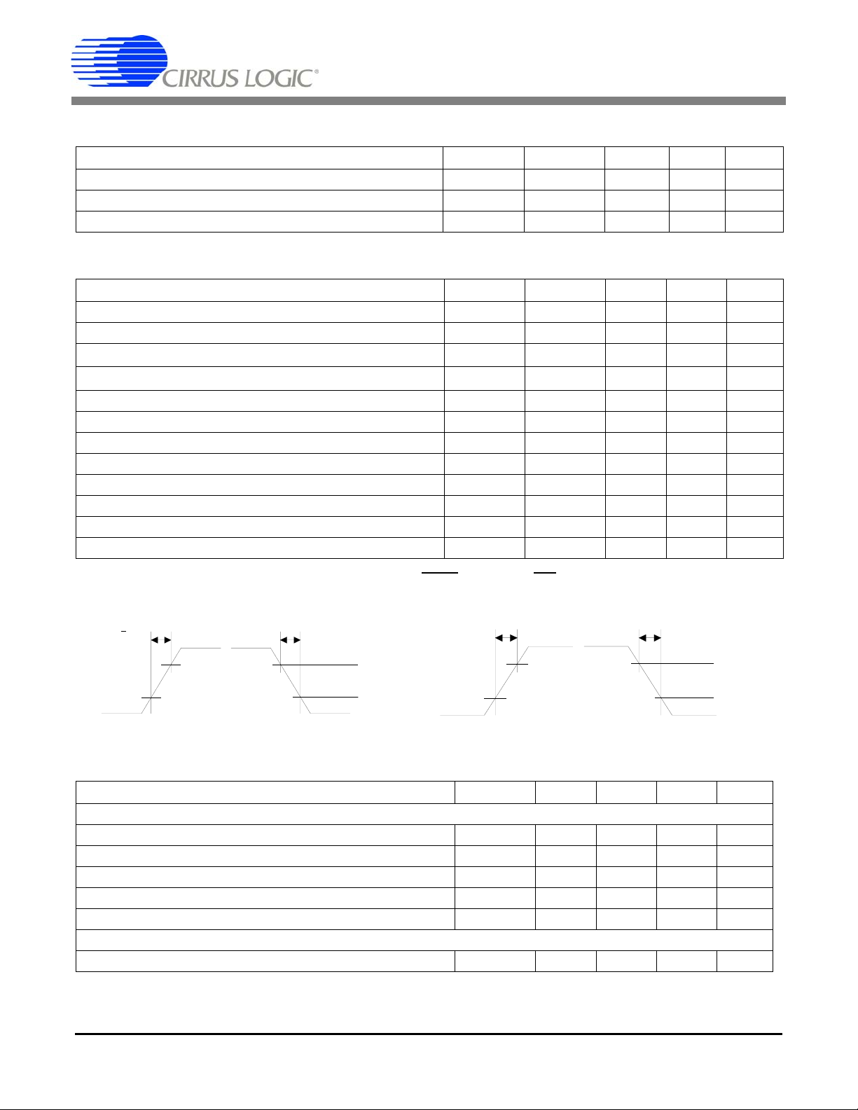
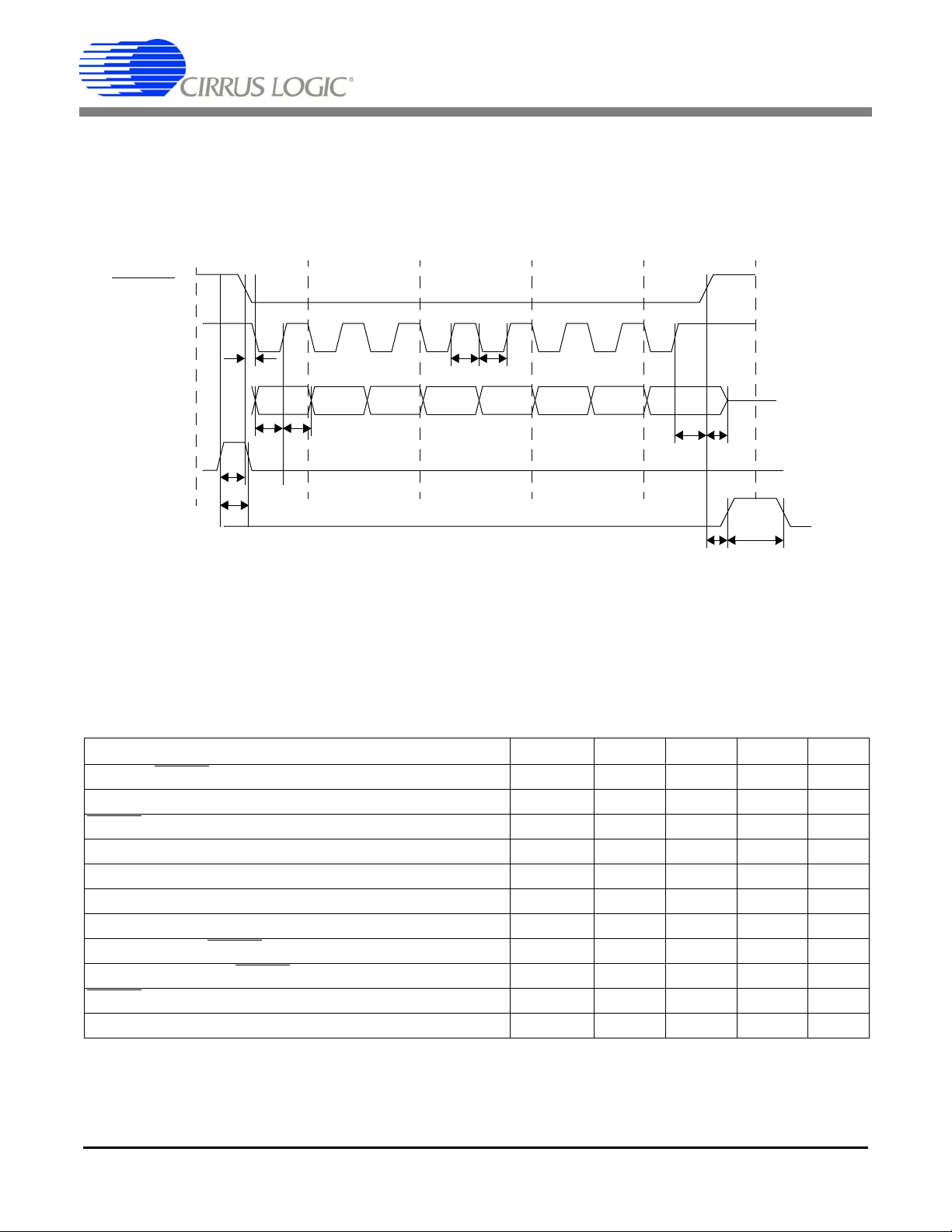
SWITCHING CHARACTERISTICS
SPI 1 Interface Timing (External Master)
SSI
CS5376A
MOSI
SCK1
SCLK
MSB MSB - 1
t
1
t
2
t
t
3
t
5
4
Figure 4. MOSI Write Timing in SPI Slave Mode
SSI
MISO
SCK1
SCLK
MSB MSB - 1 LSB
t
t
9
t
7
8
Figure 5. MISO Read Timing in SPI Slave Mode
Parameter Symbol Min Typ Max Unit
MOSI Write Timing
SSI
Enable to Valid Latch Clock t
Data Set-up Time Prior to SCK1 Rising t
Data Hold Time After SCK1 Rising t
SCK1 High Time t
SCK1 Low Time t
SCK1 Falling Prior to SSI
Disable t
MISO Read Timing
SCK1 Falling to New Data Bit t
SCK1 High Time t
SCK1 Low Time t
SSI
Rising to MISO Hi-Z t
10
LSB
t
6
t
10
1
2
3
4
5
6
7
8
9
60 - - ns
60 - - ns
120 - - ns
120 - - ns
120 - - ns
60 - - ns
- - 60 ns
120 - - ns
120 - - ns
--150ns
DS612F4 15
Page 16
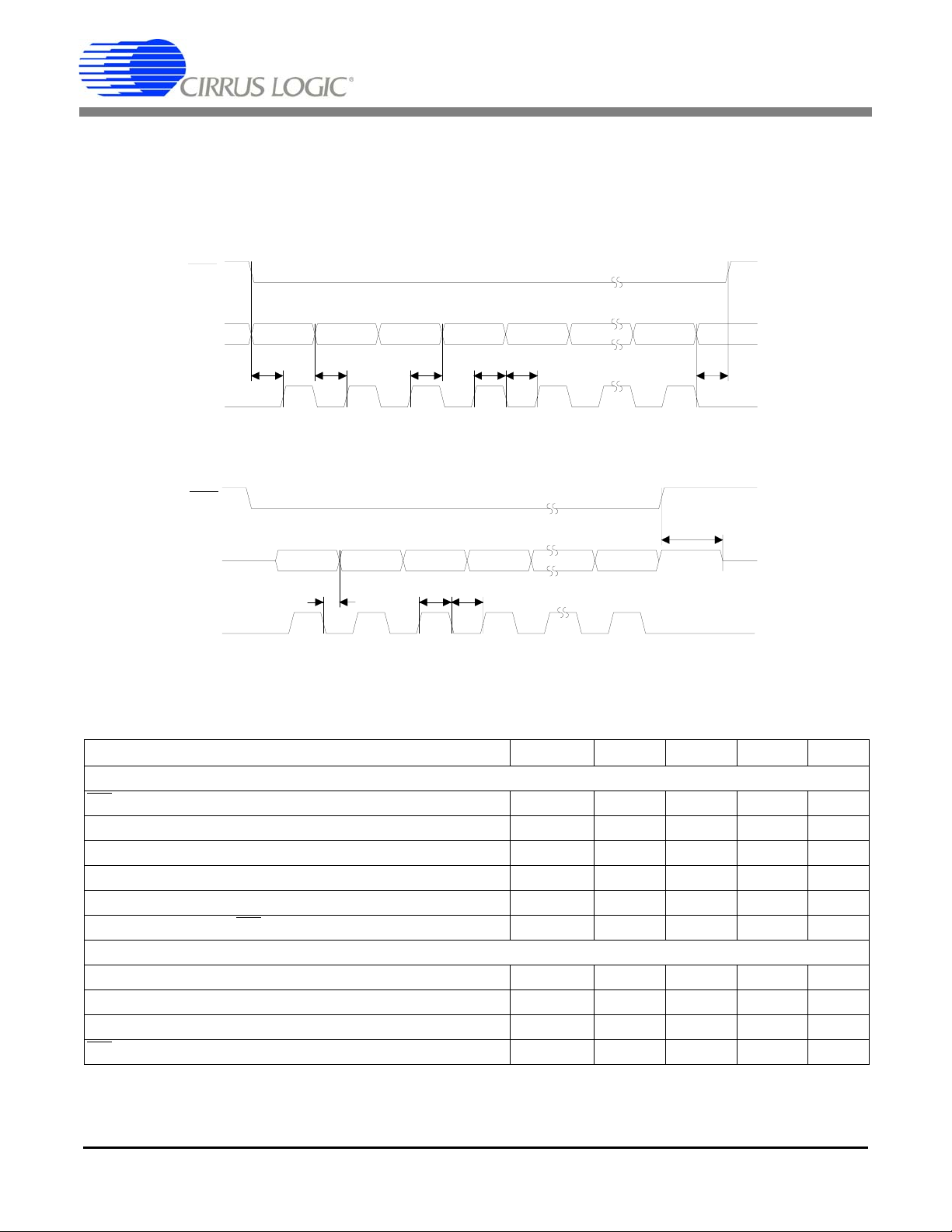
SWITCHING CHARACTERISTICS
Serial Data Port (SD Port)
SDRDY
SDCLK
t
3
SDDAT
t4t
SDTKI
SDTKO
t
1
t
2
5
CS5376A
t
t
6
7
t
t
9
8
Figure 6. SD Port Read Timing
Parameter Symbol Min Typ Max Unit
SDTKI to SDRDY Falling Edge t
SDTKI High Time Width t
SDRDY
Falling Edge to SDCLK Falling Edge t
Data Setup Time Prior to SDCLK Rising t
Data Hold Time After SDCLK Rising t
SDCLK High Time t
SDCLK Low Time t
SDCLK Rising to SDRDY
Data Hold Time After SDRDY
SDRDY
High to SDTKO Rising Edge t
Rising t
Rising t
SDTKO High Time t
10
t10t
11
1
2
3
4
5
6
7
8
9
60 - - ns
60 - 1000 ns
50 - - ns
60 - - ns
60 - - ns
120 - - ns
120 - - ns
60 - - ns
--150ns
- - 60 ns
11
90 - - ns
DS612F4 16
Page 17
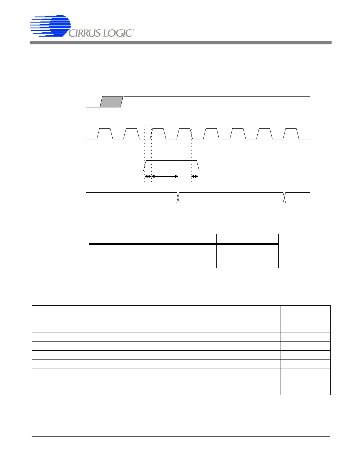
SWITCHING CHARACTERISTICS
CLK, SYNC, MCLK, MSYNC, and MDATAx
SYNC
MCLK
CS5376A
MSYNC
t
msd
MDATAx
Note: SYNC input latched on MCLK rising edge. MSYNC output triggered by MCLK falling edge.
f
MCLK
t
= T
msd
t
= T
msh
Figure 7. SYNC, MCLK, MSYNC, MDATA Interface Timing
Parameter Symbol Min Typ Max Unit
Master Clock Frequency (Note 3) CLK 32 32.768 33 MHz
Master Clock Duty Cycle DTY 40 - 60 %
Master Clock Rise Time t
Master Clock Fall Time t
Master Clock Jitter JTR - - 300 ps
Synchronization after SYNC rising (Note 4) SYNC -2 - 2 µs
MSYNC Setup Time to MCLK rising t
MCLK rising to Valid MDATA t
MSYNC falling to MCLK rising t
MCLK
MCLK
/ 4 t
t
msh
t
msd
Data1 Data2
2.048 MHz 1.024 MHz
= 122 ns t
msd
t
= 488 ns t
msh
RISE
FALL
msr
mdv
msf
msd
msh
= 244 ns
= 976 ns
- - 20 ns
- - 20 ns
20 - - ns
- - 75 ns
20 - - ns
Notes: 3. Master clock frequencies above or below 32.768 MHz will affect generated clock frequencies.
4. Sampling synchronization between multiple CS5376A devices receiving identical SYNC signals.
DS612F4 17
Page 18
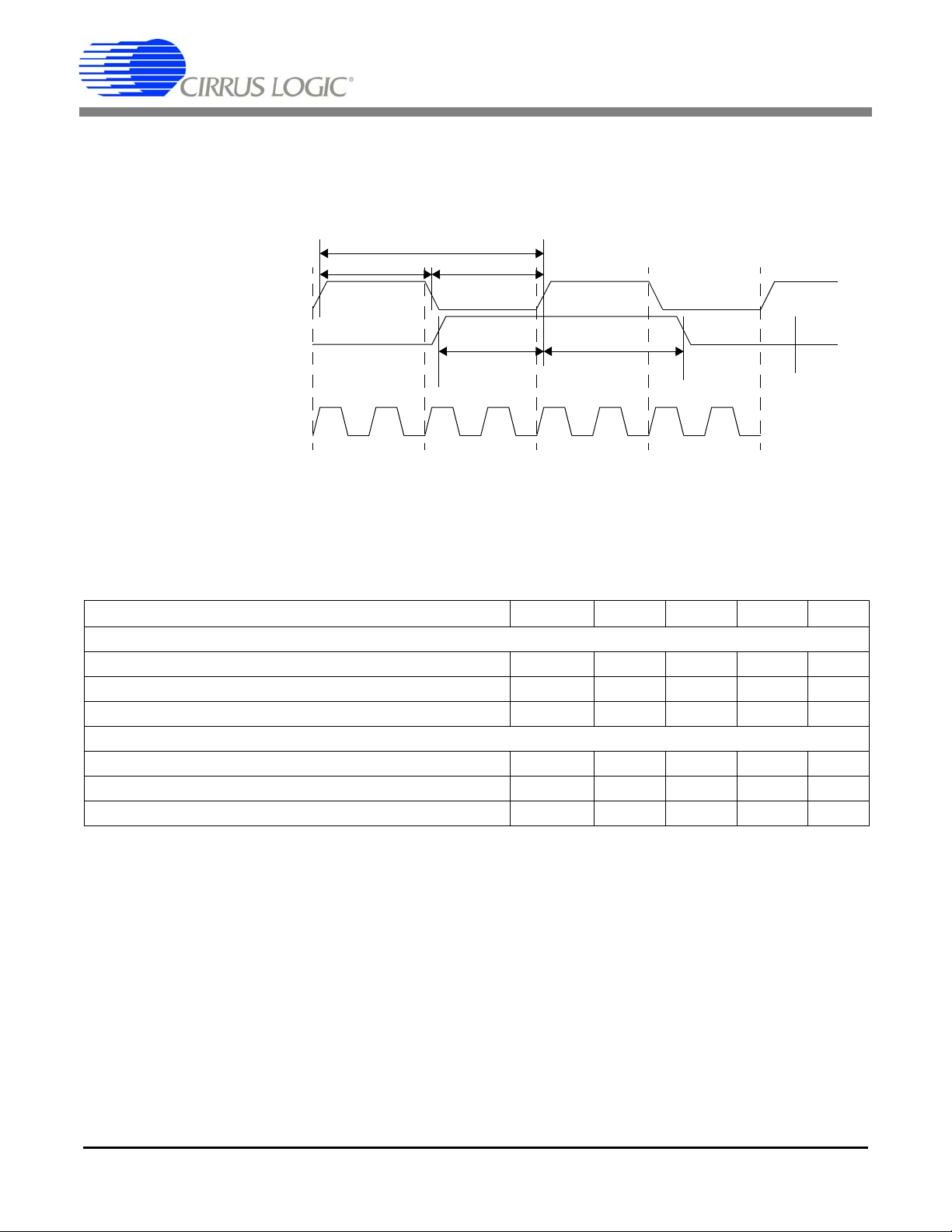
SWITCHING CHARACTERISTICS
Test Bit Stream (TBS)
t
1
t
2
TBSCLK
TBSDATA
MCLK
Note: Example timing shown for a 256 kHz output rate and no programmable delays.
Figure 8. TBS Output Clock and Data Timing
CS5376A
t
3
t
4
t
5
Parameter Symbol Min Typ Max Unit
TBS Clock Timing
TBS Clock Period t
TBS Clock High Time (Note 5) t
TBS Clock Low Time t
1
2
3
-3.906- µs
40 - 60 %
40 - 60 %
TBS Data Output Timing
TBS Data Bit Rate - 256 - kbps
TBS Data Rising to TBS Clock Rising Setup Time t
TBS Clock Rising to TBS Data Falling Hold Time (Note 6) t
4
5
60 - - ns
60 - - ns
5. TBSCLK phase can be delayed in 1/8 increments. The timing diagram shows no TBSCLK delay.
6. TBSDATA can be delayed from 0 to 63 full bit period s. The tim ing diag ram sho ws no T BSDATA delay.
DS612F4 18
Page 19
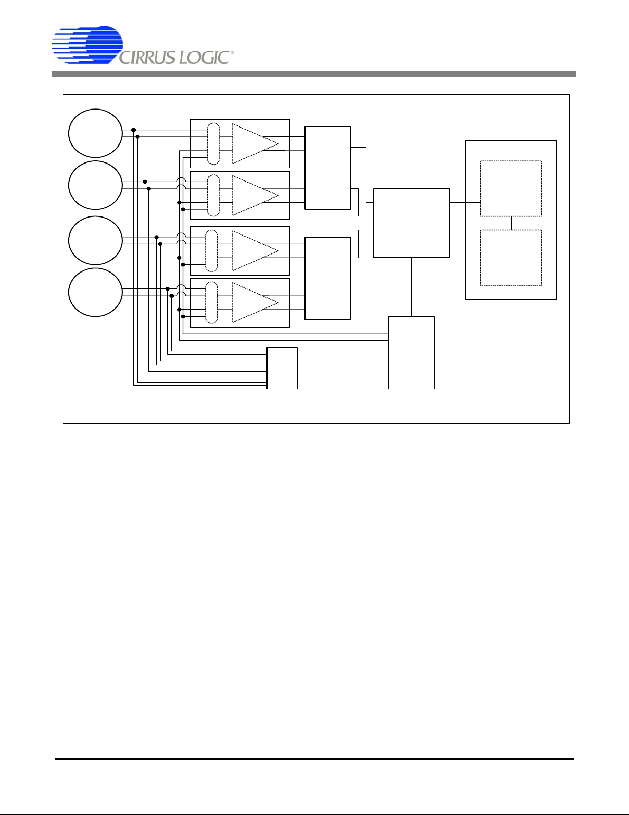
CS5376A
Geophone
or
Hydrophone
Sensor
Geophone
or
Hydrophone
Sensor
Geophone
or
Hydrophone
Sensor
Geophone
or
Hydrophone
Sensor
CS3301A
AMP
AMP
AMP
AMP
CS3302A
CS3301A
CS3302A
CS3301A
CS3302A
CS3301A
CS3302A
Switch
Switch
MUX
MUX
CS5371A
CS5372A
∆Σ
Modulator
CS5371A
CS5372A
∆Σ
Modulator
CS5376A
Digital F ilter
CS4373A
DAC
M
U
X
M
U
X
M
U
X
M
U
X
Figure 9. Multi-Channel System Block Diagram
Test
System T e lemetry
µController
or
Configuration
EEPROM
Communication
Interface
3. SYSTEM DESIGN WITH CS5376A
Figure 9 illustrates a simplified block diagram of
the CS5376A in a multi-channel measurement system.
Up to four differential sensors are connected
through CS3301A/02A differential amplifiers to
the CS5371A/72A ∆Σ modulators, where analog to
digital conversion occurs. Each modulators 1-bit
output connects to a CS5376A MDATA input,
where the oversampled ∆Σ data is decimated and
filtered to 24-bit output samples at a programmed
output rate. These output samples are buffered in
an 8-deep data FIFO and passed to the system telemetry on command.
System self tests are performed by connecting the
CS5376A test bit stream (TBS) generator to the
CS4373A test DAC. Analog tests drive differential
signals from the CS4373A test DAC into the multiplexed inputs of the CS3301A/02A amplifiers or
directly to the sensors through external analog
switches. Digital loopback tests internally connect
the TBS digital output directly to the CS5376A
modulator inputs.
3.1 Power Supplies
The multi-channel system shown in Figure 9 typically operates from a ±2.5 V analog power supply
and a 3.3 V digital power supply. The CS5376A
logic core can be powered from 3 V to minimize
power consumption, if required.
3.2 Reset Control
System reset is required only for the CS5376A device, and is a standard active low signal that can be
generated by a power supply monitor or microcontroller. Other system devices default to a powerdown state when the CS5376A is reset.
DS612F4 19
Page 20

CS5376A
3.3 Clock Generation
A single 32.768 MHz low-jitter clock input, which
can be generated from a VCXO based PLL, is required to drive the CS5376A device. Clock inputs
for other system devices are driven by clock outputs from the CS5376A.
3.4 Synchronization
Digital filter phase and analog sample timing of the
four ∆Σ modulators connected to the CS5376A are
synchronized by a rising edge on the SYNC pin. If
a synchronization signal is received identically by
all CS5376A devices in a measurement network,
synchronous sampling across the network is guaranteed.
3.5 System Configuration
Through the SPI 1 serial port, filter coefficients and
digital filter register settings can either be programmed by a microcontroller or automatically
loaded from an external EEPROM after reset. System configuration is only required for the
CS5376A device, as other devices are configured
via the CS5376A General Purpose I/O pins.
Two registers in the digital filter, SYSTEM1 and
SYSTEM2 (0x2C, 0x2D), are provided for user defined system information. These are general purpose registers that will hold any 24-bit data values
written to them.
3.6 Digital Filter Operation
After analog to digital conversion occurs in the
modulators, the oversampled 1-bit ∆Σ data is read
into the CS5376A through the MDATA pins. The
digital filter then processes data through the enabled filter stages, decimating it to 24-bit words at
a programmed output word rate. The final 24-bit
samples are concatenated with 8-bit status words
and placed into an output FIFO.
3.7 Data Collection
Data is collected from the CS5376A through the
Serial Data port (SD port). Automatically or upon
request, depending how the SDTKI pin is connected, the SD port initiates serial transactions to transfer 32-bit data from the output FIFO to the system
telemetry. The output FIFO has eight data locations
to permit latency in data collection.
3.8 Integrated peripherals
Test Bit Stream (TBS)
A digital signal generator built into the CS5376A
produces a 1-bit ∆Σ sine wave. This digital test bit
stream can be connected to the CS4373A test DAC
to create high quality analog test signals or it can be
internally looped back to the CS5376A MDATA
inputs to test the digital filter and data collection
circuitry.
Time Break
Timing information is recorded during data collection by strobing the TIMEB pin. A dedicated flag
in the sample status bits, TB, is set high to indicate
over which measurement the timing event occurred.
General Purpose I/O (GPIO)
Twelve general purpose pins are available on the
CS5376A for system control. Each pin can be set as
input or output, high or low, with an internal pullup enabled or disabled. The CS3301A/02A,
CS5371A/72A and CS4373A devices in Figure 9
are configured by simple pin settings controlled
through the CS5376A GPIO pins.
Serial Peripheral Interface 2 (SPI 2)
A secondary master mode serial port to communicate with external serial peripherals.
JTAG Port
Boundary scan JTAG is IEEE 1149.1 compliant.
20 DS612F4
Page 21
TRST
TMS
TCK
TDI
TDO
GND
VD
TBSCLK
TBSDATA
DNC
VDD2
MCLK/2
MCLK
MSYNC
MDATA4
MFLAG4
SDDAT
SYNC
CLK
TIMEB
BOOT
RESET
VDD1
GND1
SDTKI
SDTKO
SDCLK
SDRDY
64 63 62 61 60 59 58 57 56 55 54 53 52 51 50 49
1
2
3
4
5
6
VD
Pad Ring
7
8
9
10
11
12
13
14
15
16
17 18 19 20 21 22 23 24 25 26 27 28 29 30 31 32
VDD1 Pad Ring
CS5376A
VDD2 Pad Ring
SINT
Pad Ring
VD
CS5376A
MOSI
MISO
SSI
48
SCK1
47
SSO
46
GPIO11:EECS
45
GPIO10
44
GPIO9
43
GPIO8
42
GPIO7
41
GPIO6
40
VD
39
GND
38
GND2
37
GPIO5
36
GPIO4:CS4
35
GPIO3:CS3
34
GPIO2:CS2
33
GPIO1:CS1
MDATA3
MDATA2
MDATA1
MFLAG3
MFLAG2
Figure 10. Power Supply Block Diagram
4. POWER SUPPLIES
The CS5376A has three sets of power supply inputs. Two sets supply power to the I/O pins of the
device (VDD1, VDD2), and the third supplies
power to the logic core (VD). The I/O pin power
supplies determine the maximum input and output
voltages when interfacing to peripherals, and the
logic core power supply largely determines the
power consumption of the CS5376A.
4.1 Pin Descriptions
VDD1, GND1 - Pins 54,53
Sets the interface voltage to a microcontroller and
system telemetry. Can be driven with voltages from
3.3 V to 5 V.
VDD1 powers pins 1-5 and 41-64:
TRST, TMS, TCK, TDI, TDO
GND
GND2
MFLAG1
SI4
VDD2
SO
SI3
SI2
SI1
SCK2
GPIO0:CS0
GPIO6 - GPIO11:EECS
SSO
, SCK1, SSI, MISO, MOSI, SINT,
RESET
SDDAT, SDRDY
, BOOT, TIMEB, CLK, SYNC
, SDCLK, SDTKO, SDTKI
VDD2, GND2 - Pins 11, 25, 24, 38
Sets the interface voltage to the modulators, test
DAC, and serial peripherals. Can be driven with
voltages from 3.3 V to 5 V.
VDD2 powers pins 8-37:
TBSCLK, TBSDATA
MCLK/2, MCLK, MSYNC
MDATA1 - MDATA4
MFLAG1 - MFLAG4
SI1 - SI4, SO, SCK2
GPIO0:CS0 - GPIO5
DS612F4 21
Page 22

CS5376A
VD, GND - Pins 7, 40, 6, 23, 39
Sets the operational voltage of the CS5376A logic
core. Can be driven with voltages from 3 V to 5 V.
A 3 V supply minimizes total power consumption.
4.2 Bypass Capacitors
Each power supply pin should be bypassed with
parallel 1 µF and 0.01 µF caps, or by a single
0.1 µF cap, placed as close as possible to the
CS5376A. Bypass capacitors should be ceramic
(X7R, C0G), tantalum, or other good quality dielectric type.
4.3 Power Consumption
Power consumption of the CS5376A depends primarily on the power supply voltage of the logic
core (VD) and the programmed digital filter clock
rate. Digital filter clock rates are selected based on
the required output word rate as explained in “Digital Filter Initialization” on page 41.
22 DS612F4
Page 23
CS5376A
RESET
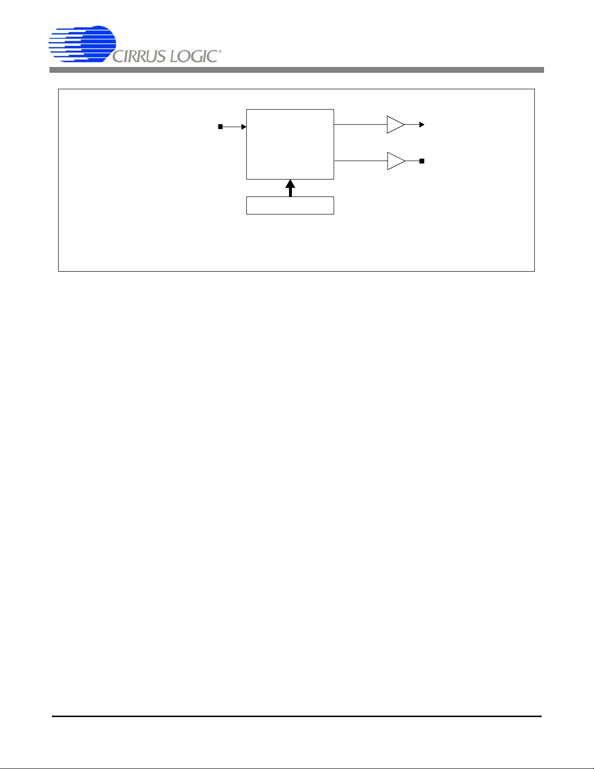
Figure 11. Reset Control Block Diagram
Self-Tests
SELFTEST
Register
5. RESET CONTROL
The CS5376A reset signal is active low. When released, a series of self-tests are performed and the
device either actively boots from an external EEPROM or enters an idle state waiting for microcontroller configuration.
5.1 Pin Descriptions
RESET - Pin 55
Reset input, active low.
BOOT - Pin 56
Boot mode select, latched following a RESET rising edge.
BOOT = 1 = EEPROM boot
BOOT = 0 = Microcontroller boot
5.2 Reset Self-Tests
After RESET is released but before booting, a series of digital filter self-tests are run. Results are
Self-Test
Type
Program ROM 0x00000A 0x00000F
Data ROM 0x0000A0 0x0000F0
Program RAM 0x000A00 0x000F00
Data RAM 0x00A000 0x00F000
Execution Unit 0x0A0000 0x0F0000
Pass
Code
Fail
Code
BOOT
Pin
1
EEPROM
Boot
0
µController
Boot
combined into the SELFTEST register (0x2F),
with 0x0AAAAA indicating all passed. Self-tests
require 60 ms to complete, after which configuration commands are serviced.
5.3 Boot Configurations
The logic state of the BOOT pin after reset determines if the CS5376A actively reads configuration
information from EEPROM or enters an idle state
waiting for a microcontroller to write configuration
commands.
EEPROM Boot
When the BOOT pin is high after reset, the
CS5376A actively reads data from an external serial EEPROM and then begins operation in the specified configuration. Configuration commands and
data are encoded in the EEPROM as specified in
the ‘Configuration By EEPROM’ section of this
data sheet, starting on page 26.
Microcontroller Boot
When the BOOT pin is low after reset, the
CS5376A enters an idle state waiting for a microcontroller to write configuration commands and
initialize filter operation. Configuration commands
and data are written as specified in the ‘Configuration By Microcontroller’ section of this data sheet,
starting on page 32.
DS612F4 23
Page 24
CS5376A
Clock DividerCLK
MCLK
Generator
DSPCFG Register
Figure 12. Clock Generation Block Diagram
6. CLOCK GENERATION
The CS5376A requires a 32.768 MHz master clock
input, which is used to generate internal digital filter clocks and external modulator clocks.
6.1 Pin Description
CLK - Pin 58
Clock input, nominal frequency 32.768 MHz.
Internal
and
Clocks
MCLK
Output
ensure recovered clocks have identical phase, system PLL designs should use a phase/frequency detector architecture.
6.3 Master Clock Jitter and Skew
Care must be taken to minimize jitter and skew in
the received master clock as both parameters affect
measurement performance.
6.2 Synchronous Clocking
To guarantee synchronous measurements throughout a sensor network, the CS5376A master clock
should be distributed to arrive at all nodes in phase.
The 32.768 MHz master clock can either be directly distributed through the system telemetry, or reconstructed locally using a VCXO based PLL. To
Jitter in the master clock causes jitter in the generated modulator clocks, resulting in sample timing
errors and increased noise.
Skew in the master clock from node to node creates
a sample timing offset, resulting in systematic measurement errors in the reconstructed signal.
24 DS612F4
Page 25
CS5376A
0
SYNC
1
MSEN
MSYNC
Generator
Figure 13. Synchronization Block Diagram
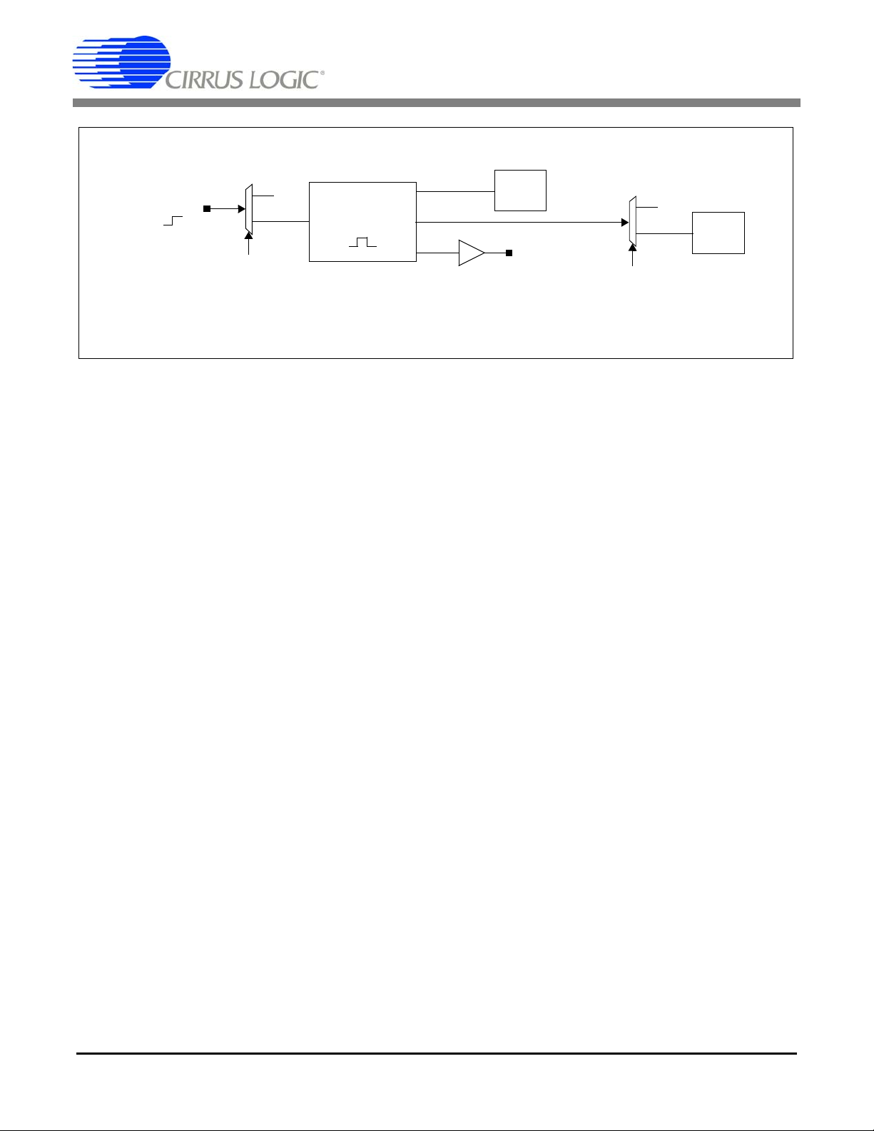
7. SYNCHRONIZATION
The CS5376A has a dedicated SYNC input that
aligns the internal digital filter phase and generates
an external signal for synchronizing modulator analog sampling. By providing simultaneous rising
edges to the SYNC pins of multiple CS5376A devices, synchronous sampling across a network can
be guaranteed.
7.1 Pin Description
SYNC - Pin 59
Synchronization input, rising edge triggered.
7.2 MSYNC Generation
Digital
Filter
MSYNC
Output
0
1
TSYNC
Tes t Bit
Stream
phase. Filter convolutions restart, and the next output word is available one full sample period later.
Repetitive synchronization is supported when
SYNC events occur at exactly the selected output
word rate. In this case, re-synchronization occurs at
the start of a convolution cycle when the digital filter state machine is already reset.
7.4 Modulator Synchronization
The external MSYNC signal phase aligns modulator analog sampling when connected to the
CS5371A/72A MSYNC input. This ensures synchronous analog sampling relative to MCLK.
The SYNC signal rising edge is used to generate a
retimed synchronization signal, MSYNC. The
MSYNC signal reinitializes internal digital filter
phase and is driven onto the MSYNC output pin to
Repetitive synchronization of the modulators is
supported when SYNC events occur at exactly the
selected output word rate. In this case, synchronization will occur at the start of analog sampling.
phase align modulator analog sampling.
The MSEN bit in the digital filter CONFIG register
(0x00) enables MSYNC generation. See “Modulator Interface” on page 39 for more information
about MSYNC.
7.5 Test Bit Stream Synchronization
When the test bit stream generator is enabled, an
MSYNC signal can reset the internal data pointer.
This restarts the test bit stream from the first data
point to establish a known output signal phase.
7.3 Digital Filter Synchronization
The internal MSYNC signal resets the digital filter
state machine to establish a known digital filter
The TSYNC bit in the digital filter TBSCFG register (0x2A) enables synchronization of the test bit
stream by MSYNC. When TSYNC is disabled, the
test bit stream phase is not affected by MSYNC.
DS612F4 25
Page 26
GPIO11:EECS
CS5376A AT25640
Figure 14. EEPROM Configuration Block Diagram
8. CONFIGURATION BY EEPROM
SCK1
MISO
MOSI
CS5376A
VD
387
46
48
50
51
WP VCC HOLD
1
CS
6
SCK
2
SO
5
SI
4
GND
After reset, the CS5376A reads the state of the
BOOT pin to determine a source for configuration
commands. If BOOT is high, the CS5376A initiates serial transactions through the SPI 1 port to
read configuration information from an external
EEPROM.
8.1 Pin Descriptions
Pins required for EEPROM boot are listed here,
other SPI 1 pins are inactive.
GPIO11:EECS - Pin 46
EEPROM chip select output, active low.
SCK1 - Pin 48
Serial clock output, nominally 1.024 MHz.
MOSI - Pin 51
Serial data output pin. Valid on rising edge of
SCK1, transition on falling edge.
MISO - Pin 50
Serial data input pin. Valid on rising edge of SCK1,
transition on falling edge.
8.2 EEPROM Hardware Interface
When booting from EEPROM the CS5376A SPI 1
port actively performs serial transactions, as shown
in Figure 15, to read configuration commands and
data. 8-bit SPI opcodes and 16-bit addresses are
combined to read back 8-bit configuration commands and 24-bit configuration data.
System design should include a connection to the
configuration EEPROM for in-circuit reprogramming. The CS5376A SPI 1 pins go high impedance
when inactive to support external connections to
the serial bus.
8.3 EEPROM Organization
The boot EEPROM holds the 8-bit commands and
24-bit data required to initialize the CS5376A into
an operational state. Configuration information
starts at memory location 0x10, with addresses
0x00 to 0x0F free for use as manufacturing header
information.
The first serial transaction reads a 1-byte command
from memory location 0x10 and then, depending
on the command type, reads multiple 3-byte data
words to complete the command. Command and
data reads continue until the ‘Filter Start’ command
is recognized.
The maximum number of bytes that can be written
for a single configuration is approximately
26 DS612F4
Page 27
CS5376A
Instruction Opcode Address Definition
Read 0x03 ADDR[15:0] Read data beginning at the address given in ADDR.
SPI 1 Read from EEPROM
SSI
MOSI
MISO
EECS
Cycle
SCK1
MOSI
READ
CMD
0x03 ADDR
2 BYTE
ADDR
ADDR
DATA1 DATA3DATA2
1 BYTE / 3 BYTE
DATA
18276543
MSB LSB
612345
MISO
EECS
MSB LSB612345
Figure 15. SPI 1 EEPROM Read Transactions
X
DS612F4 27
Page 28
Write DF Register - 0x01
CS5376A
0000h
Mfg Header
0010h
EEPROM
Manufacturing
Information
8-bit Command
N x 24-bit Data
EEPROM
Command and
8-bit Command
Data Values
N x 24-bit Data
. . .
1FFFh
Figure 16. 8 Kbyte EEPROM Memory Organization
5 KByte (40 Kbit), which includes command overhead:
Memory Requirement Bytes
Digital Filter Registers (22) 154
FIR Coefficients (255+255) 1537
IIR Coefficients (3+5) 25
Test Bit Stream Data (1024) 3076
This EEPROM command writes a data value to the
specified digital filter register. Digital filter registers control hardware peripherals and filtering
functions. See “Digital Filter Registers” on page 86
for the bit definitions of the digital filter registers.
Sample Command:
Write digital filter register 0x00 with data value
0x070431. Then write 0x20 with data 0x000240.
01 00 00 00 07 04 31
01 00 00 20 00 02 40
Write FIR Coefficients - 0x02
This EEPROM command writes custom coefficients for the FIR1 and FIR2 filters. The first two
data words set the number of FIR1 and FIR2 coefficients to be written. The remaining data words are
the concatenated FIR1 and FIR2 coefficients.
A maximum of 255 coefficients can be written for
each FIR filter, though the available digital filter
computation cycles will limit their practical size.
See “FIR Filter” on page 47 for more information
about FIR filter coefficients.
‘Filter Start’ Command 1
Sample Command:
Total Bytes 4793
Write FIR1 coefficients 0x00022E, 0x000771 then
Table 4. Maximum EEPROM Configuration
FIR2 coefficients 0xFFFFB9, 0xFFFE8D.
02 00 00 02 00 00 02
00 02 2E 00 07 71 FF FF B9 FF FE 8D
Supported serial configuration EEPROMs are
Write IIR Coefficients - 0x03
SPI mode 0 (0,0) compatible, 16-bit addresses, 8bit data, larger than 5 KByte (40 KBit). ATMEL
AT25640, AT25128, or similar serial EEPROMs
are recommended.
This EEPROM command writes custom coefficients for the two stage IIR filter. The IIR architecture and number of coefficients is fixed, so eight
data words containing coefficient values always
8.4 EEPROM Configuration Commands
immediately follow the command byte. The IIR coefficient write order is: a11, b10, b11, a21, a22,
b20, b21, and b22. See “IIR Filter” on page 55 for
A summary of available EEPROM commands is
more information about IIR filter coefficients.
shown in Table 5.
28 DS612F4
Page 29
CS5376A
Sample Command:
Write IIR1 coefficients 0x84BC9D, 0x7DA1B1,
0x825E4F, and IIR2 coefficients 0x83694F,
0x3CAD5F, 0x3E5104, 0x835DF8, 0x3E5104.
03
84 BC 9D 7D A1 B1 82 5E 4F 83 69 4F
3C AD 5F 3E 51 04 83 5D F8 3E 51 04
Write ROM Coefficients - 0x04
This EEPROM command selects the on-chip coefficients for the FIR1, FIR2, IIR 1st order, and IIR
2nd order filters for use by the digital filter. One
data word is required to select which internal coefficient sets to use. See “Filter Coefficient Selection” on page 41 for information about selecting
on-chip FIR and IIR coefficient sets.
Sample Command:
Select IIR1 and IIR2 3 Hz @ 500 SPS low-cut coefficients, with FIR1 and FIR2 linear phase highcut coefficients. Data word 0x002200.
04 00 22 00
Write TBS Data - 0x05
This EEPROM command writes a custom data set
for the test bit stream (TBS) generator. This command, along with the ability to program the test bit
stream generator interpolation and clock rate, can
create custom frequency test signals.
The first data word sets the number of TBS data to
be written and the remaining data words are the
TBS data values. See “Test Bit Stream Generator”
on page 64 for information about using custom test
bit stream data sets.
Name CMD
8-bit
NOP 00 - No Operation
WRITE DF REGISTER 01 REG
WRITE FIR COEFFICIENTS 02 NUM FIR1
WRITE IIR COEFFICIENTS 03 a11
WRITE ROM COEFFICIENTS 04 COEF SEL Use On-Chip Coefficients
WRITE TBS DATA 05 NUM TBS
WRITE ROM TBS 06 - Use On-Chip TBS Data
FILTER START 07 - Start Digital Filter Operation
DATA
24-bit
DATA
NUM FIR2
(FIR COEF)
b10
b11
a21
a22
b20
b21
b22
(TBS DATA)
Description
Write Digital Filter Register
Write Custom FIR Coefficients
Write Custom IIR Coefficients
Write Custom Test Bit Stream Data
(DATA) indicates multiple words of this type are to be written.
Table 5. EEPROM Boot Configuration Commands
DS612F4 29
Page 30

CS5376A
Sample Command:
Write test bit stream data 0x000000, 0x0007DA,
0x000FB5, 0x00178F.
05 00 00 04
00 00 00 00 07 DA 00 0F B5 00 17 8F
Write TBS ROM Data - 0x06
This EEPROM command selects the on-chip test
bit stream (TBS) data for use by the TBS generator.
No data words are required for this EEPROM command. See “Test Bit Stream Generator” on page 64
for more information about the on-chip test bit
stream data set.
Sample Command:
06
Filter Start - 0x07
This EEPROM command initializes and starts the
digital filter. Measurement data becomes available
one full sample period after this command is received. No data words are required for this EEPROM command.
Sample Command:
07
8.5 Example EEPROM Configuration
Table 6 shows an example EEPROM file for a minimal CS5376A configuration.
30 DS612F4
Page 31

CS5376A
Addr Data Description
00 00 Mfg header
01 00
02 00
03 00
04 00
05 00
06 00
07 00
08 00
09 00
0A 00
0B 00
0C 00
0D 00
0E 00
0F 00
10 04 Write ROM Coefficients
11 00
12 22
13 00
14 06 Write TBS ROM Data
15 01 Write CONFIG Register
16 00
17 00
18 00
19 07
1A 04
1B 31
1C 01 Write FILTCFG Register
1D 00
1E 00
1F 20
Addr Data Description
20 00
21 02
22 40
23 01 Write TBSCFG Register
24 00
25 00
26 2A
27 07
28 40
29 40
2A 01 Write TBSGAIN Register
2B 00
2C 00
2D 2B
2E 04
2F B0
30 00
31 07 Filter Start
Table 6. Example EEPROM File
DS612F4 31
Page 32

CS5376A
Digital Filter
Command
Interpreter
Figure 17. Serial Peripheral Interface 1 (SPI 1) Blo ck Diagram
SPI 1
Registers
9. CONFIGURATION BY MICROCONTROLLER
After reset, the CS5376A reads the state of the
BOOT pin to determine a source for configuration
commands. If BOOT is low, the CS5376A receives
configuration commands from a microcontroller.
9.1 Pin Descriptions
Pins required for microcontroller boot are listed
here, other SPI 1 pins are inactive.
SSI - Pin 49
Slave select input pin, active low. Serial chip select
input from a microcontroller.
SCK1 - Pin 48
9.2 Microcontroller Hardware Interface
When booting from a microcontroller the
CS5376A SPI 1 port receives configuration commands and configuration data through serial transactions, as shown in Figure 18. 8-bit SPI opcodes
and 8-bit addresses are combined to read and write
24-bit configuration commands and data.
Microcontroller serial transactions require toggling
the SSI pin as the CS5376A chip select and writing
a serial clock to the SCK1 input. Serial data is input
to the CS5376A on the MOSI pin, and output from
the CS5376A on the MISO pin.
SPI 1
Pin Logic
SSI
SCK1
MOSI
MISO
SINT
Serial clock input pin. Serial clock input from microcontroller, maximum 4.096 MHz.
MOSI - Pin 51
Serial data input pin. Valid on rising edge of SCK1,
transition on falling edge.
9.3 Microcontroller Serial Transactions
Microcontroller configuration commands are written to the digital filter through the SPI 1 registers.
A 24-bit command and two 24-bit data words can
be written to the SPI 1 registers in any single serial
transaction. Some commands require additional
MISO - Pin 50
Serial data output pin. Valid on rising edge of
data words through additional serial transactions to
complete.
SCK1, transition on falling edge. Open drain output requiring a 10 kΩ pull-up resistor.
SINT - Pin 52
Serial interrupt output pin, active low. 1 uS active
low pulse output when ready for next serial transaction.
32 DS612F4
9.3.1 SPI opcodes
A microcontroller communicates with the
CS5376A SPI 1 port using standard 8-bit SPI op-
codes and an 8-bit SPI address. The standard SPI
‘Read’ and ‘Write’ opcodes are listed in Figure 18.
Page 33

CS5376A
Instruction Opcode Address Definition
Write 0x02 ADDR[7:0] Write SPI1 registers beginning at the address in ADDR.
Read 0x03 ADDR[7:0] Read SPI 1 registers beginning at the address in ADDR.
Microcontroller Write to SPI 1
SSI
MOSI 0x02 ADDR Data1
MISO
Microcontroller Read from SP I 1
SSI
MOSI
MISO
Cycle
SCK1
18276543
0x03 ADDR
DataNData2
Data1 DataNData2
MOSI
MISO
SSI
MSB LSB
MSB LSB612345
612345
X
Figure 18. Microcontroller Serial Transac tions
DS612F4 33
Page 34

CS5376A
9.3.2 SPI 1 registers
The SPI 1 registers are shown in Figure 19 and are
24-bit registers mapped into an 8-bit register space
as high, mid, and low bytes. See “SPI 1 Registers”
on page 81 for the bit definitions of the SPI 1 registers.
9.3.3 SPI 1 transactions
A serial transaction to the SPI 1 registers starts with
an SPI opcode, followed by an address, and then
some number of data bytes written or read starting
at that address.
Typical serial write transactions require sending
groups of 5, 8, or 11 total bytes to the SPI1CMD or
SPI1DAT1 registers.
Example 5-byte write transaction to SPI1CMD
02 03 12 34 56
Example 5-byte write transaction to SPI1DAT1
02 06 12 34 56
Example 8-byte write transaction to SPI1CMD
02 03 12 34 56 AB CD EF
MOSI: 03 01 00
MISO: xx xx 12
5-byte read transaction of SPI1DAT1
MOSI: 03 06 00 00 00
MISO: xx xx 12 34 56
9.3.4 Multiple serial transactions
Some configuration commands require multiple se-
rial transactions to complete. There must be a small
delay between transactions for the CS5376A to
process the incoming data. Three methods can be
used to ensure the CS5376A is ready to receive the
next configuration command.
1) Delay a fixed 1 ms period to guarantee enough
time for the command to be completed.
2) Monitor the SINT pin for a 1 us active low pulse.
This pulse output occurs once the CS5376A com-
pletes processing the current command.
3) Verify the status of the E2DREQ bit by reading
the SPI1CTRL register. When low, the CS5376A is
ready for the next command.
Example 8-byte write transaction to SPI1DAT1
02 06 12 34 56 AB CD EF
Example 11-byte write transaction to SPI1CMD
02 03 12 34 56 AB CD EF 65 43 21
Typical serial read transactions require groups of 3
or 5 bytes, split between writing into MOSI and
reading from MISO.
3-byte read transaction of mid-byte of SPI1CTRL
Name Addr. Type # Bits Description
SPI1CTRL 00 - 02 R/W 8, 8, 8 SPI 1 Control
SPI1CMD 03 - 05 R/W 8, 8, 8 SPI 1 Command
SPI1DAT1 06 - 08 R/W 8, 8, 8 SPI 1 Data 1
SPI1DAT2 09 - 0B R/W 8, 8, 8 SPI 1 Data 2
Figure 19. SPI 1 Registers
9.3.5 Polling E2DREQ
One transaction type that can always be performed
no matter the delay from the previous configuration
command is reading E2DREQ in the mid-byte of
the SPI1CTRL register. A 3-byte read transaction.
MOSI: 03 01 00
MISO: xx xx 01 <- E2DREQ bit high
MISO: xx xx 00 <- E2DREQ bit low
34 DS612F4
Page 35

CS5376A
The E2DREQ bit reads high while a configuration
command is being processed. When low, the digital
filter is ready to receive a new configuration command.
9.4 Microcontroller Configuration Commands
A summary of available microcontroller configuration commands is listed in Table 7.
Write DF Register - 0x01
This configuration command writes a specified
digital filter register. Digital filter registers control
hardware peripherals and filtering functions. See
“Digital Filter Registers” on page 86 for the bit definitions of the digital filter registers.
Sample Command:
Write digital filter register 0x00 with data value
0x070431. Then write 0x20 with data 0x000240.
02 03 00 00 01 00 00 00 07 04 31
Delay 1 ms, monitor SINT, or poll E2DREQ
02 03 00 00 01 00 00 20 00 02 40
Delay 1 ms, monitor SINT, or poll E2DREQ
Read DF Register - 0x02
This command reads a specified digital filter register. The register value is requested in the first SPI
transaction, with the register value copied to
SPI1DAT1 and read in a subsequent SPI transaction.
Sample Command:
Read digital filter registers 0x00 and 0x20.
02 03 00 00 02 00 00 00
Name CMD
24-bit
NOP 000000 - - No Operation
WRITE DF REGISTER 000001 REG DATA Write Digital Filter Register
READ DF REGISTER 000002 REG
WRITE FIR COEFFICIENTS 000003 NUM FIR1
WRITE IIR COEFFICIENTS 000004 a11
WRITE ROM COEFFICIENTS 000005 COEF SEL - Use On-Chip Coefficients
WRITE TBS DATA 000006 NUM TBS
WRITE ROM TBS 000007 - - Use On-Chip TBS Data
FILTER START 000008 - - Start Digital Filter Operation
FILTER STOP 000009 - - Stop Digital Filter Operation
DAT1
24-bit
[DATA]
(FIR COEF)
b11
a22
b21
(TBS DATA)-(TBS DATA)
DAT2
24-bit
-
-
NUM FIR2
(FIR COEF)
b10
a21
b20
b22
Description
Read Digital Filter Register
Write Custom FIR Coefficients
Write Custom IIR Coefficients
Write Custom Test Bit Stream Data
[DATA] indicates data word returned from digital filter.
(DATA) indicates multiple words of this type are to be written.
Table 7. Microcontroller Boot Configuration Commands
DS612F4 35
Page 36

CS5376A
Delay 1 ms, monitor SINT, or poll E2DREQ
MOSI: 03 06 00 00 00
MISO: xx xx 07 04 31
02 03 00 00 02 00 00 20
Delay 1 ms, monitor SINT, or poll E2DREQ
MOSI: 03 06 00 00 00
MISO: xx xx 00 02 40
Write FIR Coefficients - 0x03
This command writes custom coefficients for the
FIR1 and FIR2 filters. The first two data words set
the number of FIR1 and FIR2 coefficients to be
written. The remaining data words are the concatenated FIR1 and FIR2 coefficients.
A maximum of 255 coefficients can be written for
each FIR filter, though the available digital filter
computation cycles will limit their practical size.
See “FIR Filter” on page 47 for more information
about FIR filter coefficients.
Sample Command:
Write FIR1 coefficients 0x00022E, 0x000771 then
FIR2 coefficients 0xFFFFB9, 0xFFFE8D.
02 03 00 00 03 00 00 02 00 00 02
Delay 1 ms, monitor SINT
02 06 00 02 2E 00 07 71
Delay 1 ms, monitor SINT
02 06 FF FF B9 FF FE 8D
, or poll E2DREQ
, or poll E2DREQ
Sample Command:
Write IIR1 coefficients 0x84BC9D, 0x7DA1B1,
0x825E4F, and IIR2 coefficients 0x83694F,
0x3CAD5F, 0x3E5104, 0x835DF8, 0x3E5104.
02 03 00 00 04 84 BC 9D 7D A1 B1
Delay 1 ms, monitor SINT, or poll E2DREQ
02 06 82 5E 4F 83 69 4F
Delay 1 ms, monitor SINT, or poll E2DREQ
02 06 3C AD 5F 3E 51 04
Delay 1 ms, monitor SINT
02 06 83 5D F8 3E 51 04
Delay 1 ms, monitor SINT
Write ROM Coefficients - 0x05
This configuration command selects the on-chip
coefficients for FIR1, FIR2, IIR 1st order, and IIR
2nd order filters for use by the digital filter. One
data word is required to select which internal coefficient sets to use. See “Filter Coefficient Selection” on page 41 for information about selecting
on-chip FIR and IIR coefficient sets.
, or poll E2DREQ
, or poll E2DREQ
Sample Command:
Select IIR1 and IIR2 3 Hz @ 500 SPS low-cut coefficients, with FIR1 and FIR2 linear phase highcut coefficients. Data word 0x002200.
02 03 00 00 05 00 22 00
Delay 1 ms, monitor SINT, or poll E2DREQ
Delay 1 ms, monitor SINT, or poll E2DREQ
Write IIR Coefficients - 0x04
This command writes custom coefficients for the
two stage IIR filter. The IIR architecture and number of coefficients is fixed, so eight coefficient values immediately follow this command. The IIR
coefficient write order is: a11, b10, b11, a21, a22,
b20, b21, and b22. See “IIR Filter” on page 55 for
more information about IIR filter coefficients.
36 DS612F4
Write TBS Data - 0x06
This command writes a custom data set for the test
bit stream (TBS) generator. This command, along
with the ability to program the test bit stream generator interpolation and clock rate, can create custom frequency test signals.
The first data word sets the number of TBS data to
be written and the remaining data words are the
TBS data values. See “Test Bit Stream Generator”
Page 37

CS5376A
on page 64 for information about using custom test
bit stream data sets.
Sample Command:
Write test bit stream data 0x000000, 0x0007DA,
0x000FB5, 0x00178F.
02 03 00 00 06 00 00 04
Delay 1 ms, monitor SINT, or poll E2DREQ
02 06 00 00 00 00 07 DA
Delay 1 ms, monitor SINT, or poll E2DREQ
02 06 00 0F B5 00 17 8F
Delay 1 ms, monitor SINT, or poll E2DREQ
Write TBS ROM Data - 0x07
This command selects the on-chip test bit stream
(TBS) data for use by the TBS generator. No data
words are required for this configuration command. See “Test Bit Stream Generator” on page 64
for information about the on-chip test bit stream
data set.
Sample Command:
02 03 00 00 07
Delay 1 ms, monitor SINT, or poll E2DREQ
Filter Start - 0x08
This command initializes and starts the digital filter. Measurement data becomes available one full
sample period after this command is issued. No
data words are required for this configuration command.
Sample Command:
02 03 00 00 08
Delay 1 ms, monitor SINT, or poll E2DREQ
Filter Stop - 0x09
This command disables the digital filter. Measurement data output stops immediately after this command is issued. No data words are required for this
configuration command.
Sample Command:
02 03 00 00 09
Delay 1 ms, monitor SINT, or poll E2DREQ
9.5 Example Microcontroller Configuration
Table 6 shows example microcontroller transactions for a minimal CS5376A configuration.
DS612F4 37
Page 38

Transaction SPI Data Description
01 02 03 00 00 05 00 22 00 Write ROM coefficients
02 Delay 1ms, monitor SINT
03 02 03 00 00 07 Write ROM TBS Data
04 Delay 1ms, monitor SINT
05 02 03 00 00 01 00 00 00 07 04 31 Write CONFIG Register
06 Delay 1ms, monitor SINT
07 02 03 00 00 01 00 00 20 00 02 40 Write FILTCFG Register
08 Delay 1ms, monitor SINT
09 02 03 00 00 01 00 00 2A 07 40 40 Write TBSCFG Register
10 Delay 1ms, monitor SINT
11 02 03 00 00 01 00 00 2B 04 B0 00 Write TBSGAIN Register
12 Delay 1ms, monitor SINT
13 02 03 00 00 08 Filter Start
, or poll E2DREQ
, or poll E2DREQ
, or poll E2DREQ
, or poll E2DREQ
, or poll E2DREQ
, or poll E2DREQ
CS5376A
Table 8. Example Microcontroller Configuration
DS612F4 38
Page 39

CS5376A
MCLK
MCLK/2
MSYNC
MDATA[4:1]
MFLAG[4:1]
DC Offset
& Gain
Correction
MCLK /
MSYNC
Generate
MDI Input
512 kHz
CLK
SYNC
SINC
Filter
Output to High Speed Serial Data Port (SD Port)
Figure 20. Modulator Data Interface
10.MODULATOR INTERFACE
The CS5376A performs digital filtering for up to
four ∆Σ modulators. Signals from the modulators
are connected through the modulator data interface
(MDI).
FIR
Filters
Output Rate 4000 SPS ~ 1 SPS
IIR
Filter
10.2Modulator Clock Generation
The MCLK and MCLK/2 outputs are low-jitter,
low-skew modulator clocks generated from the
32.768 MHz master clock.
10.1Pin Descriptions
MCLK, MCLK/2 - Pins 13, 12
Modulator clock outputs. Nominally 2.048 MHz
and 1.024 MHz.
MSYNC - Pin 14
Modulator synchronization signal output. Generated from the SYNC input.
MDATA1 - MDATA4 - Pins 15, 17, 19, 21
Modulator data inputs, nominally 512 kbit/s.
MFLAG1 - MFLAG4 - Pins 16, 18, 20, 22
Modulator flag inputs. Driven high when modulator is unstable due to an analog over-range signal.
MCLK typically operates at 2.048 MHz unless analog low-power modes require a 1.024 MHz modulator clock. MCLK/2 always produces a clock at
half the selected MCLK rate.
The MCLK rate is selected and the MCLK and
MCLK/2 outputs are enabled by bits in the digital
filter CONFIG register (0x00). By default MCLK
and MCLK/2 are disabled and driven low.
10.3Modulator Synchronization
The MSYNC output signal follows an input on the
SYNC pin. MSYNC phase aligns the modulator
sampling instant to guarantee synchronous analog
sampling across a measurement network.
MSYNC is enabled by a bit in the CONFIG register
(0x00). By default SYNC inputs do not cause an
MSYNC output.
DS612F4 39
Page 40

CS5376A
10.4Modulator Data Inputs
The MDATA input expects 1-bit ∆Σ data at a
512 kHz or 256 kHz rate. The input rate is selected
by a bit in the CONFIG register (0x00). By default,
MDATA is expected at 512 kHz.
The MDATA input one’s density is designed for
full scale positive at 86% and full scale negative at
14%, with absolute maximum over-range capability to 93% and 7%. These raw ∆Σ inputs are decimated and filtered by the digital filter to create 24bit samples at the output rate.
10.5Modulator Flag Inputs
A high MFLAG input signal indicates the corresponding ∆Σ modulator has become unstable due
to an analog over-range input signal. Once the
over-range signal is reduced, the modulator recovers stability and the MFLAG signal is cleared.
The MFLAG inputs are mapped to status bits in the
SD port, and are associated with each sample when
written. See “Serial Data Port” on page 61 for more
information on the MFLAG error bits in the SD
port status byte.
40 DS612F4
Page 41

CS5376A
Modulator
Input
512 kHz
SINC Filter
2 - 64000
DC Offset
& Gain
Correction
FIR1
4
Output to High Speed Serial Data Port (SD Port)
Figure 21. Digital Filter Stages
11.DIGITAL FILTER INITIALIZATION
The CS5376A digital filter consists of three multistage sections: a three stage SINC filter, a two stage
FIR filter, and a two stage IIR filter.
To initialize the digital filter, FIR and IIR coefficient sets are selected using configuration commands and the FILTCFG register (0x20) is written
to select the output filter stage, the output word
rate, and the number of enabled channels. The digital filter clock rate is selected by writing the CONFIG register (0x00).
11.1Filter Coefficient Selection
FIR2
2
Output Rate 4000 SPS ~ 1 SPS
IIR1 IIR2
1st Order
2nd Order
word, and the available coefficient sets for each selection.
Characteristics of the on-chip digital filter coefficients are discussed in the ‘SINC Filter’, ‘FIR Filter’, and ‘IIR Filter’ sections of this data sheet.
11.2Filter Configuration Options
Digital filter parameters are selected by bits in the
FILTCFG register (0x20), and the digital filter
clock rate is selected by bits in the CONFIG register (0x00).
Selection of SINC filter coefficients is not required
as they are selected automatically based on the programmed output word rate.
Digital filter FIR and IIR coefficients are selected
using the ‘Write FIR Coefficients’ and ‘Write IIR
Coefficients’, or the ‘Write ROM Coefficients’
configuration commands. When writing the FIR
and IIR coefficients from ROM, a data word selects
an on-chip coefficient set for each filter stage. Fig-
11.2.1 Output Filter Stage
The digital filter can output data following any
stage in the filter chain. The output filter stage is selected by the FSEL bits in the FILTCFG register.
Taking data from the SINC or FIR1 filter stages reduces the overall decimation of the filter chain and
increases the output rate, as discussed in the following section. Taking data from FIR2, IIR1, IIR2,
or IIR3 results in data at the selected rate.
ure 22 shows the format of the coefficient selection
DS612F4 41
Page 42

CS5376A
Bits 23:20 19:16 15:12 11:8 7:4 3:0
Selection 0000 0000 IIR2 IIR1 FIR2 FIR1
Bits 15:12 IIR2 Coefficients
0000 3 Hz @ 2000 SPS
0001 3 Hz @ 1000 SPS
0010 3 Hz @ 500 SPS
0011 3 Hz @ 333 SPS
0100 3 Hz @ 250 SPS
Figure 22. FIR and IIR Coefficient Set Selection Word
Bits 11:8 IIR1 Coefficients
0000 3 Hz @ 2000 SPS
0001 3 Hz @ 1000 SPS
0010 3 Hz @ 500 SPS
0011 3 Hz @ 333 SPS
0100 3 Hz @ 250 SPS
11.2.2 Output Word Rate
The CS5376A digital filter supports output word
rates (OWRs) between 4000 SPS and 1 SPS. The
output word rate is selected by the DEC bits in the
FILTCFG register.
When taking data directly from the SINC filter, the
decimation of the FIR1 and FIR2 stages is bypassed and the actual output word rate is multiplied
by a factor of eight compared with the register selection. When taking data directly from FIR1, the
decimation of the FIR2 stage is bypassed and the
actual output word rate is multiplied by a factor of
two. Data taken from the FIR2, IIR1, IIR2, or IIR3
filtering stages is output at the selected rate.
11.2.3 Channel Enable
Digital filtering can be performed simultaneously
for up to four ∆Σ modulators. The number of enabled channels is selected by the CH bits in the
FILTCFG register.
Channels are enabled sequentially. Selecting one
channel operation enables channel 1 only, selecting
two channel operation enables channels 1 and 2, se-
Bits 3:0 FIR1 Coefficients
0000 Linear Phase
0001 Minimum Phase
Bits 7:4 FIR2 Coefficients
0000 Linear Phase
0001 Minimum Phase
lecting three channel operation enables channels 1,
2, and 3, and selecting four channel operation enables all four channels.
11.2.4 Digital Filter Clock
The digital filter clock rate is programmable between 16.384 MHz and 32 kHz by bits in the CONFIG register.
Computation Cycles
The minimum digital filter clock rate for a configuration depends on the computation cycles required
to complete digital filter convolutions at the selected output word rate. All configurations work for a
maximum digital filter clock, but lower clock rates
consume less power.
Standby Mode
The CS5376A can be placed in a low-power standby mode by sending the ‘Filter Stop’ configuration
command and programming the digital filter clock
to 32 kHz. In this mode the digital filter idles, consuming minimal power until re-enabled by later
configuration commands.
42 DS612F4
Page 43

CS5376A
4th order
sinc3
stage3
5
1-bit
∆−Σ
Input
5th order
sinc1
4th order
sinc3
stage1
5
8
4th order
4th order
sinc3
stage2
5
sinc2
stage1
2
4th order
Figure 23. SINC Filter Block Diagram
12.SINC FILTER
The SINC filters primary purpose is to attenuate
out-of-band noise components from the ∆Σ modulators. While doing so, they decimate 1-bit ∆Σ data
into lower frequency 24-bit data suitable for the
FIR and IIR filters.
The SINC filter has three cascaded sections,
SINC1, SINC2, and SINC3, which are each made
up of the smaller stages shown in Figure 23.
sinc2
stage2
2
5th order
sinc3
stage4
2
4th order
sinc2
stage3
2
6th order
sinc3
stage5
4th order
2
sinc2
stage4
2
6th order
sinc3
stage6
3
12.2SINC2 Filter
The second section is SINC2, a multi-stage, variable order, variable decimation SINC filter. Depending on the selected output word rate in the
FILTCFG register, different cascaded SINC2 stages are enabled, as shown in Table 9.
12.3SINC3 Filter
24-bit
Output
The selected output word rate in the FILTCFG register automatically determines the coefficients and
decimation ratios selected for the SINC filters.
Once the SINC filter configuration is set, all enabled channels are filtered and decimated using an
identical hardware algorithm.
The last section is SINC3, a flexible multi-stage
variable order, variable decimation SINC filter.
Depending on the selected output word rate in the
FILTCFG register, different SINC3 stages are enabled, as shown in Table 9.
12.4SINC Filter Synchronization
12.1SINC1 Filter
The first section is SINC1, a single stage 5th order
fixed decimate by 8 SINC filter. This SINC filter
decimates the incoming 1-bit ∆Σ bit stream from
the modulators down to a 64 kHz rate.
DS612F4 43
The SINC filter is synchronized to the external system by the MSYNC signal, which is generated
from the SYNC input. The MSYNC signal sets a
reference time (time 0) for all filter operations, and
the SINC filter is restarted to phase align with this
reference time.
Page 44

SINC1 – Single stage, fixed decimate by 8
th
5
order decimate by 8, 36 coefficients
SINC2 – Multi-stage, variable decimation
Stage 1: 4
Stage 2: 4
Stage 3: 5
Stage 4: 6
th
order decimate by 2, 5 coefficients
th
order decimate by 2, 5 coefficients
th
order decimate by 2, 6 coefficients
th
order decimate by 2, 7 coefficients
SINC3 – Multi-stage, variable decimation
Stage 1: 4
Stage 2: 4
Stage 3: 4
Stage 4: 5
Stage 5: 6
Stage 6: 6
th
order decimate by 5, 17 coefficients
th
order decimate by 5, 17 coefficients
th
order decimate by 5, 17 coefficients
th
order decimate by 2, 6 coefficients
th
order decimate by 2, 7 coefficients
th
order decimate by 3, 13 coefficients
CS5376A
Figure 24. SINC Filter Stages
SINC filters
FIR2
Output
Word
Rate
4000 0111 8 2 4 - 2000 0110 8 4 3,4 - 1000 0101 8 8 2,3,4 - -
500 0100 8 16 1,2,3,4 - 333 0011 8 8 2,3,4 3 6
250 0010 8 16 1,2,3,4 2 5
200 0001 8 2 4 20 3,4,5
125 0000 8 16 1,2,3,4 4 4,5
100 1111 8 4 3,4 20 3,4,5
50 1110 8 8 2,3,4 20 3,4,5
40 1101 8 2 4 100 2,3,4,5
25 1100 8 16 1,2,3,4 20 3,4,5
20 1011 8 4 3,4 100 2,3,4,5
10 1010 8 8 2,3,4 100 2,3,4,5
5 1001 8 16 1,2,3,4 100 2,3,4,5
1 1000 8 16 1,2,3,4 500 1,2,3,4,5
DEC Bit
Setting
SINC1
Decimation
SINC2
Decimation
SINC2
Stages
SINC3
Decimation
SINC3
Stages
Ta ble 9. SINC Filter Configurations
DS612F4 44
Page 45

CS5376A
Filter Type
SINC1
th
5
order decimate by 8
36 coefficients
Filter Type
SINC2 (Stage 1)
SINC2 (Stage 2)
th
4
order decimate by 2
5 coefficients
SINC2 (Stage 3)
th
5
order decimate by 2
6 coefficients
SINC2 (Stage 4)
th
6
order decimate by 2
7 coefficients
System Function Filter Coefficients
5
8
−
⎛
1
⎜
)(
zH
=
⎜
1
⎝
⎞
z
−
⎟
1
−
⎟
z
−
⎠
= 1 h18 = 2460
h
0
h
= 5 h19 = 2380
1
= 15 h20 = 2226
h
2
h
= 35 h21 = 2010
3
= 70 h22 = 1750
h
4
h
= 126 h23 = 1470
5
h
= 210 h24 = 1190
6
= 330 h25 = 926
h
7
h
= 490 h26 = 690
8
= 690 h27 = 490
h
9
h
= 926 h28 = 330
10
h
= 1190 h29 = 210
11
= 1470 h30 = 126
h
12
h
= 1750 h31 = 70
13
= 2010 h32 = 35
h
14
h
= 2226 h33 = 15
15
h
= 2380 h34 = 5
16
= 2460 h35 = 1
h
17
System Function Filter Coefficients
4
2
−
⎛
1
⎜
)(
zH
=
⎜
1
⎝
⎞
z
−
⎟
1
−
⎟
z
−
⎠
= 1
h
0
h
= 4
1
= 6
h
2
h
= 4
3
= 1
h
4
5
2
−
⎛
1
⎜
)(
zH
=
⎜
1
⎝
⎞
z
−
⎟
1
−
⎟
z
−
⎠
h
h
h
h
h
h
0
1
2
3
4
5
= 1
= 5
= 10
= 10
= 5
= 1
6
2
−
⎛
1
⎜
)(
zH
=
⎜
1
⎝
⎞
z
−
⎟
1
−
⎟
z
−
⎠
h
h
h
h
h
h
h
0
1
2
3
4
5
6
= 1
= 6
= 15
= 20
= 15
= 6
= 1
Table 10. SINC1 and SINC2 Filter Coefficients
DS612F4 45
Page 46

CS5376A
Filter Type
SINC3 (Stage 1)
SINC3 (Stage 2)
SINC3 (Stage 3)
th
4
order decimate by 5
17 coefficients
SINC3 (Stage 4)
th
order decimate by 2
5
6 coefficients
SINC3 (Stage 5)
th
order decimate by 2
6
7 coefficients
SINC3 (Stage 6)
th
6
order decimate by 3
13 coefficients
System Function Filter Coefficients
4
h
= 1
5
−
⎛
1
⎜
)(
zH
=
⎜
1
⎝
⎞
z
−
⎟
1
−
⎟
z
−
⎠
0
h
= 4
1
h
h
h
h
h
h
h
h
h
h
h
h
h
h
h
2
3
4
5
6
7
8
9
10
11
12
13
14
15
16
= 10
= 20
= 35
= 52
= 68
= 80
= 85
= 80
= 68
= 52
= 35
= 20
= 10
= 4
= 1
5
h
= 1
2
−
⎛
1
⎜
)(
zH
=
⎜
1
⎝
⎞
z
−
⎟
1
−
⎟
z
−
⎠
0
= 5
h
1
h
= 10
2
= 10
h
3
h
= 5
4
h
= 1
5
6
h
= 1
2
−
⎛
1
⎜
)(
zH
=
⎜
1
⎝
⎞
z
−
⎟
1
−
⎟
z
−
⎠
0
= 6
h
1
h
= 15
2
= 20
h
3
h
= 15
4
h
= 6
5
= 1
h
6
6
h
= 1
3
−
⎛
1
⎜
)(
zH
=
⎜
1
⎝
⎞
z
−
⎟
1
−
⎟
z
−
⎠
0
h
= 6
1
h
h
h
h
h
h
h
h
h
h
h
2
3
4
5
6
7
8
9
10
11
12
= 21
= 50
= 90
= 126
= 141
= 126
= 90
= 50
= 21
= 6
= 1
Table 11. SINC3 Filter Coefficients
DS612F4 46
Page 47

FIR1 Filter - decimate by 4 FIR2 Filter - decimate by 2
13.FIR FILTER
CS5376A
Figure 25. FIR Filter Block Diagram
The finite impulse response (FIR) filter block consists of two cascaded stages, FIR1 and FIR2. It
compensates for SINC filter droop and creates a
low-pass corner to block aliased components of the
input signal.
On-chip linear phase or minimum phase coefficients can be selected using a configuration command, or the coefficients can be programmed for a
custom filter response.
13.1FIR1 Filter
The FIR1 filter stage has a decimate by four architecture. It compensates for SINC filter droop and
flattens the magnitude response of the pass band.
The on-chip linear and minimum phase coefficient
sets are 48-tap, with a maximum 255 programmable coefficients. All coefficients are normalized to
24-bit two’s complement full scale, 0x7FFFFF.
The characteristic equation for FIR1 is a convolution of the input values, X(n), and the filter coefficients, h(k), to produce an output value, Y.
Y = [h(k)*X(n-k)] + [h(k+1)*X(n-(k+1))] + ...
13.2FIR2 Filter
The FIR2 filter stage has a decimate by two architecture. It creates a low-pass brick wall filter to
block aliased components of the input signal.
The on-chip linear and minimum phase coefficient
sets are 126-tap, with a maximum 255 programmable coefficients. All coefficients are normalized to
24-bit two’s complement full scale, 0x7FFFFF.
The characteristic equation for FIR2 is a convolution of the input values, X(n), and the filter coefficients, h(k), to produce an output value, Y.
Y = [h(k)*X(n-k)] + [h(k+1)*X(n-(k+1))] + ...
13.3On-Chip FIR Coefficients
Two sets of on-chip linear phase and minimum
phase coefficients are available for FIR1 and FIR2.
Performance of the on-chip coefficient sets is very
good, with excellent ripple and stop band characteristics as described in Figure 26 and Table 12.
Which on-chip coefficient set to use is selected by
a data word following the ‘Write ROM Coefficients’ configuration command. See “Filter Coefficient Selection” on page 41 for information about
selecting on-chip coefficient sets.
DS612F4 47
Page 48

CS5376A
13.4Programmable FIR Coefficients
A maximum of 255 + 255 coefficients can be programmed into FIR1 and FIR2 to create a custom
filter response. The total number of coefficients for
the FIR filter is fundamentally limited by the available computation cycles in the digital filter, which
itself is determined by the digital filter clock rate.
Custom filter sets should normalize the maximum
coefficient value to 24-bit two’s complement full
scale, 0x7FFFFF, and scale all other coefficients
accordingly. To maintain maximum internal dynamic range, the CS5376A FIR filter performs
double precision calculations with an automatic
gain correction to scale the final output.
Custom FIR coefficients are uploaded using the
‘Write FIR Coefficients’ configuration command.
See “EEPROM Configuration Commands” on
page 28 or “Microcontroller Configuration Commands” on page 35 for information about writing
custom FIR coefficients.
13.5FIR Filter Synchronization
The FIR1 and FIR2 filters are synchronized to the
external system by the MSYNC signal, which is
generated from the SYNC input. The MSYNC signal sets a reference time (time 0) for all filter operations, and the FIR filters are restarted to phase
align with this reference time.
48 DS612F4
Page 49

FIR1 – Single stage, fixed decimate by 4
Coefficient set 0: linear phase decimate by 4, 48 coefficients
Coefficient set 1: minimum phase decimate by 4, 48 coefficients
SINC droop compensation filter
FIR2 – Single stage, fixed decimate by 2
Coefficient set 0: linear phase decimate by 2, 126 coefficients
Coefficient set 1: minimum phase decimate by 2, 126 coefficients
Brick wall low-pass filter, flat to 40% f
Combined SINC + FIR digital filter specifications
Passband ripple less than +/- 0.01 dB below 40% f
Transition band -3 dB frequency at 42.89% f
Stopband attenuation greater than 130 dB above 50% f
Figure 26. FIR Filter Stages
CS5376A
s
s
s
s
SINC + FIR filters
FIR2
Output
Word
Rate
4000 16 4 2 128 0.0042 130.38
2000 32 4 2 256 0.0045 130.38
1000 64 4 2 512 0.0040 130.42
500 128 4 2 1024 0.0041 130.42
333 192 4 2 1536 0.0080 130.45
250 256 4 2 2048 0.0064 130.43
200 320 4 2 2560 0.0041 130.43
125 512 4 2 4096 0.0046 130.42
100 640 4 2 5120 0.0040 130.43
50 1280 4 2 10240 0.0040 130.43
40 1600 4 2 12800 0.0036 130.43
25 2560 4 2 20480 0.0040 132.98
20 3200 4 2 25600 0.0036 130.43
10 6400 4 2 51200 0.0036 130.43
5 12800 4 2 102400 0.0036 130.43
1 64000 4 2 512000 0.0029 134.31
SINC
Decimation
FIR1
Decimation
T able 12. FIR Filter Characteristics
FIR2
Decimation
Total
Decimation
Passband
Ripple
±
(
dB)
Stopband
Attenuation
(dB)
DS612F4 49
Page 50

CS5376A
Individual filter stage group delay (no IIR)
Decimation
Ratios
SINC1
SINC2
Stage 4 2 7 3.0
Stages 3,4 2,2 6,7 8.5
Stages 2,3,4 2,2,2 5,6,7 19.0
Stages 1,2,3,4 2,2,2,2 5,5,6,7 40.0
SINC3
Stage 6 3 13 6.0
Stage 5 2 7 3.0
Stages 4,5 2,2 6,7 8.5
Stages 3,4,5 5,2,2 17,6,7 50.5
Stages 2,3,4,5 5,5,2,2 17,17,6,7 260.5
Stages 1,2,3,4,5 5,5,5,2,2 17,17,17,6,7 1310.5
FIR1
Coefficient Set 0 4 48 23.5
Coefficient Set 1 4 48 See Figure
FIR2
Coefficient Set 0 2 126 62.5
Coefficient Set 1 2 126 See Figure
8 36 17.5
Cumulative linear phase group delay (no IIR)
FIR2
Output
Word
Rate
4000 41.5 417.5 4417.5 34.5117
2000 85.5 837.5 8837.5 34.5215
1000 169.5 1673.5 17673.5 34.5186
500 337.5 3345.5 35345.5 34.5171
333 553.5 5065.5 53065.5 34.5479
250 721.5 6737.5 70737.5 34.5398
200 849.5 8369.5 88369.5 34.5193
125 1425.5 13457.5 141457.5 34.5355
100 1701.5 16741.5 176741.5 34.5198
50 3401.5 33481.5 353481.5 34.5197
40 4209.5 41809.5 441809.5 34.5164
25 6801.5 66961.5 706961.5 34.5196
20 8421.5 83621.5 883621.5 34.5165
10 16841.5 167241.5 1767241.5 34.5164
5 33681.5 334481.5 3534481.5 34.5164
1 168081.5 1672081.5 17672081.5 34.5158
SINC Output
Group Delay
(SINC Filter
Input Rate)
FIR1 Output
Group Delay
(SINC Filter
Input Rate)
Table 13. SINC + FIR Group Delay
Number of
Coefficients
FIR2 Output
Group Delay
(SINC Filter
Input Rate)
Group Delay
(Filter Stage
Input Rate)
FIR2 Output
Group Delay
(FIR2 Output
Word Rate)
DS612F4 50
Page 51

Minimum phase group delay
FIR1
Minimum
Phase Group
Delay
(Normalized
frequency)
CS5376A
FIR2
Minimum
Phase Group
Delay
(Normalized
frequency)
Figure 27. Minimum Phase Group Delay
DS612F4 51
Page 52

Filter Type Filter Coefficients
(normalized 24-bit)
FIR1 (Coefficient set 0)
Low pass, SINC compensation
Linear phase decimate by 4
48 coefficients
= 558 h24 = 8388607
h
0
= 1905 h25 = 7042723
h
1
= 3834 h26 = 4768946
h
2
= 5118 h27 = 2266428
h
3
= 365 h28 = 189436
h
4
= -14518 h29 = -1053303
h
5
= -39787 h30 = -1392827
h
6
= -67365 h31 = -1084130
h
7
= -69909 h32 = -496361
h
8
= -19450 h33 = 39864
h
9
= 97434 h34 = 332367
h
10
= 258881 h35 = 375562
h
11
= 375562 h36 = 258881
h
12
= 332367 h37 = 97434
h
13
= 39864 h38 = -19450
h
14
= -496361 h39 = -69909
h
15
= -1084130 h40 = -67365
h
16
= -1392827 h41 = -39787
h
17
= -1053303 h42 = -14518
h
18
= 189436 h43 = 365
h
19
= 2266428 h44 = 5118
h
20
= 4768946 h45 = 3834
h
21
= 7042723 h46 = 1905
h
22
= 8388607 h47 = 558
h
23
FIR1 (Coefficient set 1)
Low pass, SINC compensation
Minimum phase decimate by 4
48 coefficients
= 3337 h24 = 555919
h
0
= 22258 h25 = -165441
h
1
= 88284 h26 = -581479
h
2
= 266742 h27 = -617500
h
3
= 655747 h28 = -388985
h
4
= 1371455 h29 = -99112
h
5
= 2502684 h30 = 114761
h
6
= 4031988 h31 = 186557
h
7
= 5783129 h32 = 141374
h
8
= 7396359 h33 = 58582
h
9
= 8388607 h34 = -12664
h
10
= 8325707 h35 = -42821
h
11
= 6988887 h36 = -35055
h
12
= 4531706 h37 = -16792
h
13
h
= 1507479 h38 = 367
14
= -1319126 h39 = 7929
h
15
= -3207750 h40 = 5926
h
16
= -3736028 h41 = 2892
h
17
= -2980701 h42 = 23
h
18
= -1421498 h43 = -1164
h
19
= 237307 h44 = -538
h
20
= 1373654 h45 = -238
h
21
= 1711919 h46 = 18
h
22
= 1322371 h47 = 113
h
23
Table 14. FIR1 Coefficients
CS5376A
DS612F4 52
Page 53

Filter Type Filter Coefficients
(normalized 24-bit)
FIR2 (Coefficient set 0)
Low pass, passband to 40% f
Linear phase decimate by 2
126 coefficients
s
h0 = -71 h63 = 8388607
h
= -371 h64 = 3875315
1
h
= -870 h65 = -766230
2
= -986 h66 = -1854336
h
3
h
= 34 h67 = -137179
4
= 1786 h68 = 1113788
h
5
h
= 2291 h69 = 454990
6
= 291 h70 = -642475
h
7
h
= -2036 h71 = -553873
8
= -943 h72 = 298975
h
9
h
= 2985 h73 = 533334
10
= 3784 h74 = -49958
h
11
h
= -1458 h75 = -443272
12
h
= -5808 h76 = -116005
13
h
= -1007 h77 = 318763
14
= 7756 h78 = 208018
h
15
h
= 5935 h79 = -187141
16
= -7135 h80 = -238025
h
17
h
= -11691 h81 = 68863
18
= 3531 h82 = 221211
h
19
h
= 17500 h83 = 22850
20
= 4388 h84 = -174452
h
21
h
= -20661 h85 = -81993
22
= -15960 h86 = 114154
h
23
h
= 18930 h87 = 109009
24
= 29808 h88 = -54172
h
25
= -9795 h89 = -109189
h
26
h
= -42573 h90 = 4436
27
= -7745 h91 = 90744
h
28
h
= 49994 h92 = 29702
29
= 33021 h93 = -62651
h
30
h
= -47092 h94 = -47092
31
= -62651 h95 = 33021
h
32
h
= 29702 h96 = 49994
33
= 90744 h97 = -7745
h
34
h
= 4436 h98 = -42573
35
= -109189 h99 = -9795
h
36
h
= -54172 h
37
= 109009 h
h
38
h
= 114154 h
39
= -81993 h
h
40
h
= -174452 h
41
= 22850 h
h
42
h
= 221211 h
43
= 68863 h
h
44
h
= -238025 h
45
= -187141 h
h
46
h
= 208018 h
47
= 318763 h
h
48
h
= -116005 h
49
= -443272 h
h
50
= -49958 h
h
51
h
= 533334 h
52
= 298975 h
h
53
h
= -553873 h
54
= -642475 h
h
55
h
= 454990 h
56
= 1113788 h
h
57
h
= -137179 h
58
= -1854336 h
h
59
h
= -766230 h
60
= 3875315 h
h
61
h
= 8388607 h
62
= 29808
100
= 18930
101
= -15960
102
= -20661
103
= 4388
104
= 17500
105
= 3531
106
= -11691
107
= -7135
108
= 5935
109
= 7756
110
= -1007
111
= -5808
112
= -1458
113
= 3784
114
= 2985
115
= -943
116
= -2036
117
= 291
118
= 2291
119
= 1786
120
= 34
121
= -986
122
= -870
123
= -371
124
= -71
125
Table 15. FIR2 Linear Phase Coefficients
CS5376A
DS612F4 53
Page 54

Filter Type Filter Coefficients
(normalized 24-bit)
FIR2 (Coefficient set 1)
Low pass, passband to 40% f
Minimum phase decimate by 2
126 coefficients
s
h0 = 4019 h63 = 67863
h
= 43275 h64 = -190800
1
h
= 235427 h65 = -128546
2
= 848528 h66 = 114197
h
3
h
= 2240207 h67 = 147750
4
h
= 4525758 h68 = -46352
5
h
= 7077833 h69 = -143269
6
h
= 8388607 h70 = -13290
7
h
= 6885673 h71 = 114721
8
h
= 2483461 h72 = 51933
9
h
= -2538963 h73 = -75952
10
h
= -4800543 h74 = -68746
11
h
= -2761696 h75 = 38171
12
h
= 1426109 h76 = 68492
13
h
= 3624338 h77 = -7856
14
h
= 1820814 h78 = -57526
15
h
= -1695825 h79 = -12540
16
= -2885148 h80 = 41717
h
17
h
= -605252 h81 = 23334
18
h
= 2135021 h82 = -25516
19
h
= 1974197 h83 = -26409
20
h
= -630111 h84 = 11717
21
h
= -2168177 h85 = 24246
22
h
= -750147 h86 = -1620
23
h
= 1516192 h87 = -19248
24
h
= 1550127 h88 = -4610
25
h
= -508445 h89 = 13356
26
h
= -1686937 h90 = 7526
27
h
= -437822 h91 = -7887
28
h
= 1308705 h92 = -8016
29
h
= 1069556 h93 = 3559
30
h
= -657282 h94 = 7023
31
h
= -1301014 h95 = -598
32
h
= -30654 h96 = -5350
33
h
= 1173754 h97 = -1097
34
h
= 579643 h98 = 3579
35
h
= -803111 h99 = 1806
36
h
= -895851 h
37
h
= 328399 h
38
h
= 962522 h
39
h
= 124678 h
40
h
= -820948 h
41
h
= -466657 h
42
h
= 545674 h
43
= 652827 h
h
44
h
= -220448 h
45
h
= -680495 h
46
h
= -80886 h
47
h
= 578844 h
48
= 306445 h
h
49
h
= -395302 h
50
= -431004 h
h
51
h
= 181900 h
52
= 454403 h
h
53
h
= 15856 h
54
= -395525 h
h
55
h
= -166123 h
56
h
= 284099 h
57
h
= 253485 h
58
h
= -152407 h
59
h
= -277888 h
60
h
= 28526 h
61
h
= 250843 h
62
= -2058
100
= -1859
101
= 936
102
= 1558
103
= -224
104
= -1129
105
= -152
106
= 718
107
= 290
108
= -395
109
= -290
110
= 178
111
= 227
112
= -53
113
= -151
114
= -5
115
= 86
116
= 23
117
= -42
118
= -22
119
= 17
120
= 14
121
= -5
122
= -7
123
= 1
124
= 3
125
Table 16. FIR2 Minimum Phase Coefficients
CS5376A
DS612F4 54
Page 55

CS5376A
1st Order IIR1
b
10
-1
Z
-a
11
b
11
3rd Order IIR3 implemented by
running both IIR1 and IIR2 stages
Figure 28. IIR Filter Block Diagram
14.IIR FILTER
The infinite impulse response (IIR) filter block
consists of two cascaded stages, IIR1 and IIR2. It
creates a high-pass corner to block very low-frequency and DC components of the input signal.
2nd Order IIR2
b
-a
-a
21
22
20
-1
Z
b
21
-1
Z
b
22
The characteristic equations for the 1st order IIR
include an input value, X, an output value, Y, and
two intermediate values, W1 and W2, separated by
a delay element (z
-1
).
On-chip IIR1 and IIR2 coefficients can be selected
using a configuration command, or the coefficients
can be programmed for a custom filter response.
14.1IIR Architecture
The architecture of the IIR filter is automatically
determined when the output filter stage is selected
in the FILTCFG register. Selecting the 1st order
IIR1 filter bypasses the 2nd order stage, while selecting the 2nd order IIR2 filter bypasses the 1st order stage. Selection of the 3rd order IIR3 filter
enables both the 1st and 2nd order stages.
14.2IIR1 Filter
The 1st order IIR filter stage is a direct form filter
with three coefficients: a11, b10, and b11. Coefficients of a 1st order IIR are inherently normalized
to one, and should be scaled to 24-bit two’s complement full scale, 0x7FFFFF.
W2 = W1
W1 = X + (-a11 * W2)
Y = (W1 * b10) + (W2 * b11)
14.3IIR2 Filter
The 2nd order IIR filter stage is a direct form filter
with five coefficients: a21, a22, b20, b21, and b22.
Coefficients of a 2nd order IIR are inherently normalized to two, and should be scaled to 24-bit
two’s complement full scale, 0x7FFFFF. Normalization effectively divides the 2nd order coefficients in half relative to the input, and requires
modification of the characteristic equations.
The characteristic equations for the 2nd order IIR
include an input value, X, an output value, Y, and
three intermediate values, W3, W4, and W5, each
separated by a delay element (z-1). The following
DS612F4 55
Page 56

CS5376A
characteristic equations model the operation of the
2nd order IIR filter with unnormalized coefficients.
W5 = W4
W4 = W3
W3 = X + (-a21 * W4) + (-a22 * W5)
Y = (W3 * b20) + (W4 * b21) + (W5 * b22)
Internally, the CS5376A uses normalized coeffi-
cients to perform the 2nd order IIR filter calculation, which changes the algorithm slightly. The
following characteristic equations model the operation of the 2nd order IIR filter when using normalized coefficients.
W5 = W4
W4 = W3
W3 = 2 * [(X / 2) + (-a21 * W4) + (-a22 * W5)]
Y = 2 * [(W3 * b20) + (W4 * b21) + (W5 * b22)]
14.4IIR3 Filter
The 3rd order IIR filter is implemented by running
both the 1st order and 2nd order IIR filter stages. It
can be modeled by cascading the characteristic
equations of the 1st order and 2nd order IIR stages.
14.5On-Chip IIR Coefficients
Five sets of on-chip coefficients are available for
IIR1 and IIR2, each providing a 3 Hz high-pass
Butterworth response at different output word
rates. Characteristics of the on-chip coefficient sets
are described in Figure 29 and Table 17.
Which on-chip coefficient set to use is selected by
a data word following the ‘Write ROM Coefficients’ configuration command. See “Filter Coefficient Selection” on page 41 for information about
selecting on-chip coefficient sets.
14.6Programmable IIR Coefficients
A maximum of 3 + 5 coefficients can be programmed into IIR1 and IIR2 to create a custom filter response. Custom filter sets should normalize
the coefficients to 24-bit two’s complement full
scale, 0x7FFFFF. To maintain maximum internal
dynamic range, the CS5376A IIR filter performs
double precision calculations with an automatic
gain correction to scale the final output.
Custom IIR coefficients are uploaded using the
‘Write IIR Coefficients’ configuration command.
See “EEPROM Configuration Commands” on
page 28 or “Microcontroller Configuration Commands” on page 35 for information about writing
custom IIR coefficients.
14.7IIR Filter Synchronization
The IIR filter is not synchronized to the external
system directly, only indirectly through the synchronization of the SINC and FIR filters. Because
IIR filters have ‘infinite’ memory, a discontinuity
in the input data stream from a synchronization
event can require significant time to settle out. The
exact settling time depends on the size of the discontinuity and the filter coefficient characteristics.
56 DS612F4
Page 57

IIR1 – Single stage, no decimation
st
order no decimation, 3 coefficients
1
Coefficient set 0: high-pass, corner 0.15% f
Coefficient set 1: high-pass, corner 0.30% f
Coefficient set 2: high-pass, corner 0.60% f
Coefficient set 3: high-pass, corner 0.90% f
Coefficient set 4: high-pass, corner 1.20% f
IIR2 – Single stage, no decimation
nd
order no decimation, 5 coefficients
2
Coefficient set 0: high-pass, corner 0.15% f
Coefficient set 1: high-pass, corner 0.30% f
Coefficient set 2: high-pass, corner 0.60% f
Coefficient set 3: high-pass, corner 0.90% f
Coefficient set 4: high-pass, corner 1.20% f
IIR3 – Two stage, no decimation
rd
order no decimation, 8 coefficients
3
(Combined IIR1 and IIR2 filter responses)
Coefficient set 0,0: high-pass, corner 0.20% f
Coefficient set 1,1: high-pass, corner 0.41% f
Coefficient set 2,2: high-pass, corner 0.82% f
Coefficient set 3,3: high-pass, corner 1.22% f
Coefficient set 4,4: high-pass, corner 1.63% f
CS5376A
(3 Hz at 2000 SPS)
s
(3 Hz at 1000 SPS)
s
(3 Hz at 500 SPS)
s
(3 Hz at 333 SPS)
s
(3 Hz at 250 SPS)
s
(3 Hz at 2000 SPS)
s
(3 Hz at 1000 SPS)
s
(3 Hz at 500 SPS)
s
(3 Hz at 333 SPS)
s
(3 Hz at 250 SPS)
s
(4 Hz at 2000 SPS)
s
(4 Hz at 1000 SPS)
s
(4 Hz at 500 SPS)
s
(4 Hz at 333 SPS)
s
(4 Hz at 250 SPS)
s
Figure 29. IIR Filter Stages
IIR filters
IIR1 Coeff
Selection
0 0.15% fs 0 0.15% fs 0,0 0.2041% fs
1 0.30% fs 1 0.30% fs 1,1 0.4074% fs
2 0.60% fs 2 0.60% fs 2,2 0.8152% fs
3 0.90% fs 3 0.90% fs 3,3 1.2222% fs
4 1.20% fs 4 1.20% fs 4,4 1.6293% fs
DS612F4 57
IIR1
Corner
Frequency
IIR2 Coeff
Selection
IIR2
Corner
Frequency
Table 17. IIR Filter Characteristics
IIR3 Coeff
Selection
IIR3
Corner
Frequency
Page 58

CS5376A
Filter Type System Function Filter Coefficients
(normalized 24-bit)
IIR1 (Coefficient set 0)
st
1
order, high pass
Corner at 0.15% f
3 coefficients
IIR1 (Coefficient set 1)
st
1
order, high pass
Corner at 0.30% f
3 coefficients
IIR1 (Coefficient set 2)
st
1
order, high pass
Corner at 0.60% f
3 coefficients
IIR1 (Coefficient set 3)
st
1
order, high pass
Corner at 0.90% f
3 coefficients
IIR1 (Coefficient set 4)
st
1
order, high pass
Corner at 1.20% f
3 coefficients
Filter Type System Function Filter Coefficients
IIR2 (Coefficient set 0)
nd
2
order, high pass
Corner at 0.15% f
5 coefficients
IIR2 (Coefficient set 1)
nd
2
order, high pass
Corner at 0.30% f
5 coefficients
IIR2 (Coefficient set 2)
nd
2
order, high pass
Corner at 0.60% f
5 coefficients
IIR2 (Coefficient set 3)
nd
2
Order, high pass
Corner at 0.90% f
5 coefficients
IIR2 (Coefficient set 4)
nd
2
order, high pass
Corner at 1.20% f
5 coefficients
s
s
s
s
s
s
s
s
s
s
⎛
+
⎜
=
)(
zH
⎜
+
1
⎝
⎛
+
⎜
=
)(
zH
⎜
+
1
⎝
⎛
+
⎜
=
)(
zH
⎜
+
1
⎝
⎛
+
⎜
=
)(
zH
⎜
+
1
⎝
⎛
+
⎜
=
)(
zH
⎜
+
1
⎝
⎛
⎜
=
zH
)(
⎜
1
⎝
⎛
⎜
=
)(
zH
⎜
1
⎝
⎛
⎜
=
)(
zH
⎜
1
⎝
⎛
⎜
=
)(
zH
⎜
1
⎝
⎛
⎜
=
zH
)(
⎜
1
⎝
1
⎞
zbb
1110
⎟
−−1
⎟
za
11
⎠
1
⎞
zbb
1110
⎟
−−1
⎟
za
11
⎠
1
⎞
zbb
1110
⎟
−−1
⎟
za
11
⎠
1
⎞
zbb
1110
⎟
−−1
⎟
za
11
⎠
1
⎞
zbb
1110
⎟
−−1
⎟
za
11
⎠
1
++
2120
1
++
21
1
++
2120
1
++
21
1
++
2120
1
++
21
1
++
2120
1
++
21
1
++
2120
1
++
21
1
−−
⎞
zbzbb
22
⎟
−−
1
⎟
zaza
22
⎠
−−
1
⎞
zbzbb
22
⎟
−−
1
⎟
zaza
22
⎠
1
−−
⎞
zbzbb
22
⎟
−−
1
⎟
zaza
22
⎠
−−
1
⎞
zbzbb
22
⎟
−−
1
⎟
zaza
22
⎠
1
−−
⎞
zbzbb
22
⎟
−−
1
⎟
zaza
22
⎠
Table 18. IIR Filter Coefficients
= -8309916
a
11
b
= 8349262
10
b
= -8349262
11
= -8231957
a
11
b
= 8310282
10
b
= -8310282
11
= -8078179
a
11
b
= 8233393
10
b
= -8233393
11
= -7927166
a
11
b
= 8157887
10
b
= -8157887
11
= -7778820
a
11
b
= 8083714
10
b
= -8083714
11
(normalized 24-bit)
a
= -8332704
21
a
= 4138771
22
b
= 4166445
20
= -8332890
b
21
b
= 4166445
22
a
= -8276806
21
a
= 4083972
22
b
= 4138770
20
= -8277540
b
21
b
= 4138770
22
a
= -8165041
21
a
= 3976543
22
b
= 4083972
20
= -8167944
b
21
b
= 4083972
22
a
= -8053350
21
a
= 3871939
22
b
= 4029898
20
= -8059796
b
21
b
= 4029898
22
a
= -7941764
21
a
= 3770088
22
b
= 3976539
20
= -7953078
b
21
b
= 3976539
22
58 DS612F4
Page 59

CS5376A
4
Gain
Correction
MDI Input
512 kHz
4
Offset
Calibration
Offset
Correction
4
SINC
Filter
4
Figure 30. Gain and Offset Correction
15.GAIN AND OFFSET CORRECTION
The CS5376A digital filter can apply independent
gain and offset corrections to the data of each measurement channel. Also, an offset calibration algorithm can automatically calculate offset correction
values for each channel.
Gain correction values are written to the GAINx
registers (0x21-0x24), while offset correction values are written to the OFFSETx registers (0x250x28). Gain and offset corrections are enabled by
the USEGR and USEOR bits in the FILTCFG register (0x20).
FIR
Filters
Output to High Speed Serial Data Port (SD Port)
Output Rate 4000 SPS ~ 1 SPS
IIR
Filter
nally calculated correction values to be written into
the GAINx registers (0x21-0x24).
Gain correction values are 24-bit two’s complement with unity gain defined as full scale,
0x7FFFFF. Gain correction always scales to a fractional value, and can never gain the digital filter
data greater than one.
Output Value = Data * (GAIN / 0x7FFFFF)
Unity Gain: GAIN = 0x7FFFFF
50% Gain: GAIN = 0x3FFFFF
When enabled, the offset calibration algorithm will
automatically calculate offset correction values for
each channel and write them into the OFFSETx
registers. Offset calibration is enabled by writing
Zero Gain: GAIN = 0x000000
Once the GAIN registers are written, the USEGR
bit in the FILTCFG register enables gain correction.
the EXP and ORCAL bits in FILTCFG.
15.2Offset Correction
15.1Gain Correction
Offset correction in the CS5376A cancels the DC
Gain correction in the CS5376A normalizes sensor
gains in multi-sensor networks. It requires exter-
DS612F4 59
bias of a measurement channel by subtracting the
Page 60

CS5376A
value in the OFFSETx registers (0x25-0x28) from
the digital filter output data word.
Offset correction values are 24-bit two’s complement with a maximum positive value of 0x7FFFFF,
and a maximum negative value of 0x800000. If applying an offset correction causes the final result to
exceed a 24-bit two’s complement maximum, the
output data will saturate to that maximum value.
Output Data = Input Data - Offset Correction
Max Positive Output Value = 0x7FFFFF
Max Negative Output Value = 0x800000
Once the OFFSET registers are written, the USEOR bit in the FILTCFG register enables offset correction.
15.3Offset Calibration
An offset calibration algorithm in the CS5376A
can automatically calculate offset correction values. When using the offset calibration algorithm,
background noise data should be used as the basis
for calculating the offset value of each measurement channel.
The offset calibration algorithm is an exponential
averaging function that places increased weight on
more recent digital filter data. The exponential
weighting factor is set by the EXP bits in the
FILTCFG register, with larger exponent values
producing a smoother averaging function that requires a longer settling time, and smaller values
producing a noisier averaging function that requires a shorter settling time. Typical exponential
values range from 0x05 to 0x0F, depending on the
available settling time.
The characteristic equations of the offset calibration algorithm include an input value, X, an output
value, Y, a summation value, YSUM, a sample index, n, and an exponential value, EXP.
Y(n) = X(n) - [YSUM(n-1) >> EXP]
YSUM(n) = Y(n) + YSUM(n-1)
Offset Correction = YSUM >> EXP
Once the EXP bits are written, the ORCAL bit in
the FILTCFG register is set to enable offset calibration. When enabled, updated offset correction values are automatically written to the OFFSETx
registers. When the offset calibration algorithm is
fully settled, the ORCAL bit is cleared to maintain
the final values in the OFFSETx registers.
60 DS612F4
Page 61

CS5376A
System Telemetry
Token Out
Data Ready
Clock Out
Data In
Token In
Figure 31. Serial Data Port Block Diagram
16.SERIAL DATA PORT
Once digital filtering is complete, each 24-bit output sample is combined with an 8-bit status byte.
These 32-bit data words are written to an 8-deep
FIFO buffer and then transmitted to the communications channel through a high speed serial data
port (SD port).
16.1Pin Descriptions
SDTKI - Pin 64
Token input, requests an SD port transaction.
SDRDY - Pin 61
Data ready output signal, active low. Open drain
output requiring a 10 kΩ pull-up resistor.
CS5376A
SDTKI
SDRDY
SDCLK
SDDAT
SDTKO
16.2SD Port Data Format
Serial data transactions transfer 32-bit words. Each
word consists of an 8-bit status byte followed by a
24-bit output sample. The status byte, shown in
Figure 32, has an MFLAG bit, channel bits, a time
break bit, and a FIFO overflow bit.
MFLAG Bit - MFLAG
The MFLAG bit is set when an MFLAG signal is
received on the MFLAG1-MFLAG4 pins. When
received, that channel MFLAG bit is set in the next
output word. See “Modulator Interface” on page 39
for more information about MFLAG.
Channel Bits - CH[1:0]
SDCLK - Pin 62
Serial clock input.
Channel bits indicate from which conversion channel the data word is from. The channel number,
CH[1:0], is zero based.
SDDAT - Pin 60
CH[1:0] = 00 = Channel 1
Serial data output. Data valid on rising edge of
SDCLK, transition on falling edge.
SDTKO - Pin 63
Token output, ends an SD port transaction. Passes
through the SDTKI signal when no data is available
in the SD port output FIFO.
CH[1:0] = 01 = Channel 2
CH[1:0] = 10 = Channel 3
CH[1:0] = 11 = Channel 4
Time Break Bit - TB
The time break bit marks a timing reference based
on a rising edge into the TIMEB pin. After a programmed delay, the TB bit in the status byte is set
for one output sample in all channels. The TIME-
DS612F4 61
Page 62

CS5376A
Word 1 Word 4
Status Data
MFLAG
31 2930 28 27 26 25 24
0 - Modulator Ok
1 - Modulator Error
--
Word 2
128 bits
Status
CH[1] CH[0]
00 - Channel 1
01 - Channel 2
10 - Channel 3
11 - Channel 4
Figure 32. SD Port Data Format
Word 3
--
0 - No Time Break
1 - Time Break
Data
TB
--
02331
W
0 - FIFO Ok
1 - FIFO Overflow
BRK digital filter register (0x29) programs the
sample delay for the TB bit output. See “Time
Break Controller” on page 67 for more information
about time break.
FIFO Overflow Bit - W
The FIFO overflow bit indicates an error condition
in the SD port data FIFO, and is set if new digital
filter data overwrites a FIFO location containing
data which has not yet been sent.
The W bit is sticky, meaning it persists indefinitely
once set. Clearing the W bit requires sending the
‘Filter Stop’ and ‘Filter Start’ configuration commands to reinitialize the data FIFO.
Conversion Data Word
The lower 24-bits of the SD port output data word
is the conversion sample for the specified channel.
Conversion data is 24-bit two’s complement format.
16.3SD Port Transactions
The SD port can operate in two modes depending
how the SDTKI pin is connected: request mode
where data is output when requested by the communications channel, or continuous mode where
data is output immediately when ready.
16.3.1Request Mode
To initiate SD port transactions on request, SDTKI
is connected to an active high polling signal from
the communications channel. A rising edge into
SDTKI when new data is available in the SD port
FIFO causes the CS5376A to initiate an SD port
transaction by driving SDRDY
yet available in the SD port FIFO, the SDTKI signal is passed through to the SDTKO output.
Once an SD port transaction is initiated, serial
clocks into SDCLK cause data to be output to
SDDAT, as shown in Figure 33. When all available
low. If data is not
62 DS612F4
Page 63

SDTKI
SDTKO
SDRDY
SDCLK
CS5376A
SDDAT
MSB
Figure 33. SD Port Transaction
data is read from the SD port data FIFO, SDRDY is
released and SDTKO is pulsed high for 100 nS.
16.3.2Continuous Mode
To have the CS5376A automatically initiate SD
port transactions whenever data becomes available,
connect SDTKI to a 4 MHz or slower clock source
such as MCLK/2. The first rising edge into SDTKI
after data becomes available in the SD port FIFO
LSB
causes the CS5376A to initiate an SD port transaction by driving SDRDY
low. If data is not available
in the SD port FIFO, the SDTKI signal is passed
through to the SDTKO output.
Once an SD port transaction is initiated, serial
clocks into SDCLK cause data to be output to
SDDAT, as shown in Figure 33. When all available
data is read from the SD port data FIFO, SDRDY
is
released and SDTKO is pulsed high for 100 nS.
DS612F4 63
Page 64

Digital Filter
Data Bus
CS5376A
24-bit
TBSGAIN Register
24-bit
Digital ∆Σ Modulator
1-bit
TBSDATA
Figure 34. Test Bit Stream Generator Block Diagram
17.TEST BIT STREAM GENERATOR
The CS5376A test bit stream (TBS) generator creates sine wave ∆Σ bit stream data to drive an external test DAC. The TBS digital output can also be
internally connected to the MDATA inputs for
loopback testing of the digital filter.
17.1Pin Descriptions
TBSDATA - Pin 9
Test bit stream 1-bit ∆Σ data output.
TBSCLK - Pin 8
Test bit stream clock output. Not used by the
CS4373A test DAC.
17.2TBS Architecture
The test bit stream generator consists of a data interpolator and a digital ∆Σ modulator. It receives
periodic 24-bit data from the digital filter to create
a 1-bit ∆Σ data output on the TBSDATA pin. It also
creates a clock signal at the data rate, output to the
TBSCLK pin.
The TBS input data from the digital filter is scaled
by the TBSGAIN register (0x2B). Maximum stable
amplitude is 0x04FFFF, with 0x04B8F2 approximately full scale for the CS4373A test DAC. The
TBSCFG Register
Clock Generation
TBSCLK
full scale 1-bit ∆Σ output from the TBS generator is
defined as 25% minimum and 75% maximum
one’s density.
17.3TBS Configuration
Configuration options for the TBS generator are set
through the TBSCFG register (0x2A). Gain scaling
of the TBS generator output is set by the TBSGAIN
register (0x2B).
Interpolation Factor - INTP[7:0]
Selects how many times the interpolator uses a data
point when generating the output bit stream. Interpolation is zero based and represents one greater
than the programmed register value.
Clock Rate - RATE[2:0]
Selects the TBSDATA and TBSCLK output rate.
Synchronization - TSYNC
Enables synchronization of the TBS output phase
to the MSYNC signal.
Clock Delay - CDLY[2:0]
Programs a fractional delay for TBSCLK with a 1/8
clock period resolution.
64 DS612F4
Page 65

Test Bit Stream Characteristic Equation:
(Signal Freq) * (# TBS Data) * (Interpolation + 1) = Output Rate
Example: (31.25 Hz) * (1024) * (0x07 + 1) = 256 kHz
CS5376A
Signal
Frequency
(TBSDATA)
10.00 Hz 256 kHz 0x4 0x18
10.00 Hz 512 kHz 0x5 0x31
25.00 Hz 256 kHz 0x4 0x09
25.00 Hz 512 kHz 0x5 0x13
31.25 Hz 256 kHz 0x4 0x07
31.25 Hz 512 kHz 0x5 0x0F
50.00 Hz 256 kHz 0x4 0x04
50.00 Hz 512 kHz 0x5 0x09
125.00 Hz 256 kHz 0x4 0x01
125.00 Hz 512 kHz 0x5 0x03
Table 19. TBS Configurations Using On-chip Data
Output
Rate
(TBSCLK)
Loopback - LOOP
Enables digital loopback from the TBS output to
the MDATA inputs.
Run - RUN
Enables the test bit stream generator.
Data Delay - DDLY[5:0]
Programs full period delays for TBSDATA, up to a
maximum of 63 bits.
Gain - TBSGAIN[23:0]
Scales the amplitude of the sine wave output. Maximum 0x04FFFF, nominal 0x04B8F2.
17.4TBS Data Source
Data to create test signals is loaded into digital filter memory by configuration commands. The onchip sine wave data is suitable for most tests,
Output Rate
Selection
(RATE)
Interpolation
Selection
(INTP)
though custom data is required to support custom
signal frequencies. See “EEPROM Configuration
Commands” on page 28 or “Microcontroller Configuration Commands” on page 35 for information
about programming TBS data.
TBS ROM Data
An on-chip 24-bit 1024 point digital sine wave is
stored on the CS5376A. When selected by the
‘Write TBS ROM Data’ configuration command,
the TBS generator can produce the test signal frequencies listed in Table 19. Additional discrete test
frequencies and output rates can be programmed
with the on-chip data by varying the interpolation
factor and output rate.
Custom TBS Data
If a required test frequency cannot be generated using the on-chip test bit stream data, a custom data
DS612F4 65
Page 66

CS5376A
set can be written into the CS5376A. The number
of data points to write, up to a maximum of 1024,
depends on the required test signal frequency, output rate, and available interpolation factors. Custom data sets must be continuous on the ends; i.e.
when copied end-to-end the data set must produce
a smooth curve.
17.5TBS Sine Wave Output
The TBS generator uses data from digital filter
memory to create a sine wave test signal that can
drive a test DAC. Sine wave frequency and output
data rate are calculated as shown by the characteristic equation of Table 19.
The sine wave maximum ∆Σ one’s density output
from the TBS generator is set by the TBSGAIN
register. TBSGAIN can be programmed up to a
maximum of 0x04FFFF, with the TBS generator
unstable for higher amplitudes. For the CS4373A
test DAC, a gain value of 0x04B8F2 produces an
approximately full scale sine wave output (5 V
differential).
pp
MDATA inputs. This loopback mode provides a
fully digital signal path to test the TBS generator,
digital filter, and data collection interface. Digital
loopback testing expects 512 kHz ∆Σ data for the
MDATA inputs.
A mismatch of the TBS generator full scale output
and the MDATA full scale input results in an amplitude mismatch when testing in loopback mode.
The TBS generator outputs a 75% maximum one’s
density, while the MDATA inputs expect an 86%
maximum one’s density from a ∆Σ modulator, resulting in a measured full scale error of -3.6 dB.
17.7TBS Synchronization
When the TSYNC bit is set in the TBSCFG register, the MSYNC signal resets the sine wave data
pointer and phase aligns the TBS signal output.
Once the digital filter is settled, all CS5376A devices receiving the SYNC signal will have identical
TBS signal phase. See “Synchronization” on
page 25 for more information about the SYNC and
MSYNC signals.
17.6TBS Loopback Testing
Included as part of the CS5376A test bit stream
generator is a feedback path to the digital filter
If TSYNC is clear, MSYNC has no effect on the
TBS data pointer and no change in the TBS output
phase will occur during synchronization.
66 DS612F4
Page 67

CS5376A
TIMEB
Figure 35. Time Break Block Diagram
TIMEBRK
Delay Counter
18.TIME BREAK CONTROLLER
A time break signal is used to mark timing events
that occur during measurement. An external signal
sets a flag in the status byte of an output sample to
mark when the external event occurred.
A rising edge input to the TIMEB pin causes the
TB timing reference flag to be set in the SD port
status byte. When set, the TB flag appears for only
one output sample in the status byte of all enabled
channels. The TB flag output can be delayed by
programming a sample delay value into the TIMEBRK digital filter register.
TB Flag
in SD Port
Status Byte
18.3Time Break Delay
The TIMEBRK register (0x29) sets a sample delay
between a received rising edge on the TIMEB pin
and writing the TB flag into the SD port status byte.
The programmable sample counter can compensate
for group delay through the digital filters. When the
proper group delay value is programmed into the
TIMEBRK register, the TB flag will be set in the
status byte of the measurement sample taken when
the timing reference signal was received.
18.1Pin Description
TIMEB - Pin 57
Time break input pin, rising edge triggered.
18.2Time Break Operation
An externally generated timing reference signal applied to the TIMEB pin initiates an internal sample
counter. After a number of output samples have
passed, programmed in the TIMEBRK digital filter
register (0x29), the TB flag is set in the status byte
of the SD port output word for all enabled channels.
The TB flag is automatically cleared for subsequent data words, and appears for only one output
sample in each channel.
18.3.1Step Input and Group Delay
A simple method to empirically measure the step
response and group delay of a CS5376A measurement channel is to use the time break signal as both
a timing reference input and an analog step input.
When a rising edge is received on the TIMEB pin
with no delay programmed into the TIMEBRK register, the TB flag is set in the next SD port status
byte. The same rising edge can act as a step input to
the analog channel, propagating through the digital
filter to appear as a rising edge in the measurement
data. By comparing the timing of the TB status flag
output and the rising edge in the measurement data,
the measurement channel group delay can be determined.
DS612F4 67
Page 68
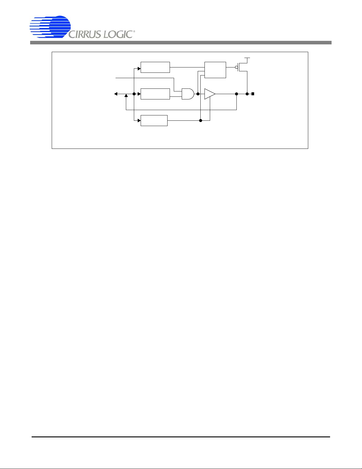
CS5376A
GP_PULL
CS output from SPI
Data bit
GP_DATA
GP_DIR
Figure 36. GPIO Bi-directional Structure
19.GENERAL PURPOSE I/O
The General Purpose I/O (GPIO) block provides 12
general purpose pins to interface with external
hardware.
19.1Pin Descriptions
GPIO[4:0]:CS[4:0] - Pins 32 - 36
Standard GPIO pins also used as SPI 2 chip selects.
GPIO[5:10] - Pins 37, 41 - 45
Standard GPIO pins.
GPIO11:EECS - Pin 46
Standard GPIO pin also used as an SPI 1 chip select
when booting from an external EEPROM.
Pull Up
Logic
R
GPIO/CS
sponding GPIO pin should be initialized as output
mode and logical 1 to produce the chip select falling edge.
19.3GPIO Registers
When used as standard GPIO pins, settings are programmed in the GPCFG0 and GPCFG1 registers.
GP_DIR bits set the input/output mode, GP_PULL
bits enable/disable the internal pull-up resistor, and
GP_DATA bits set the output data value. After reset, GPIO pins default as inputs with pull-up resistors enabled.
19.4GPIO Input Mode
19.2GPIO Architecture
Each GPIO pin can be configured as input or output, high or low, with a weak (~200 kΩ) internal
pull-up resistor enabled or disabled. Several GPIO
pins also double as chip selects for the SPI 1 and
When reading a value from the GP_DATA bits, the
returned data reports the current state of the pins. If
a pin is externally driven high it reads a logical 1, if
externally driven low it reads a logical 0. When a
GPIO pin is used as an input, the pull-up resistor
should be disabled to save power if it isn’t required.
SPI 2 serial ports. Figure 36 shows the structure of
a bi-directional GPIO pin with SPI chip select func-
19.5GPIO Output Mode
tionality.
When a GPIO pin is programmed as an output with
When the CS5376A is used as an SPI master, either
when booting from EEPROM using SPI 1 or performing master mode transactions using SPI 2, the
chip select signals from SPI 1 and SPI 2 are logically AND-ed with the GPIO data bit. The corre-
68 DS612F4
a data value of 0, the pin is driven low and the internal pull-up resistor is automatically disabled.
When programmed as an output with a data value
of 1, the pin is driven high and the pull-up resistor
is inconsequential.
Page 69

CS5376A
Any GPIO pin can be used as an open-drain output
by setting the data value to 0, enabling the pull-up,
and using the GP_DIR direction bits to control the
pin value. This open-drain output configuration
uses the internal pull-up resistor to hold the pin
high when GP_DIR is set as an input, and drives the
pin low when GP_DIR is set as an output.
19.5.1GPIO Reads in Output Mode
When reading GPIO pins the GP_DATA register
value always reports the current state of the pins, so
a value written in output mode does not necessarily
read back the same value. If a pin in output mode is
written as a logical 1, the CS5376A attempts to
drive the pin high. If an external device forces the
pin low, the read value reflects the pin state and returns a logical 0. Similarly, if an output pin is written as a logical 0 but forced high externally, the
read value reflects the pin state and returns a logical
1. In both cases the CS5376A is in contention with
the external device resulting in increased power
consumption.
DS612F4 69
Page 70

Digital
Filter
SCKFS[2:0] / SCKPO / SCKPH
SPI2EN[4:1] / RCH[1:0]
Pin logic
4:1
CS5376A
SCK2
SO
SI1
SI2
SI3
SI4
CS[4:0]
Figure 37. Serial Peripheral Interface 2 (SPI 2) Block Diagram
20.SERIAL PERIPHERAL INTERFACE 2
The Serial Peripheral Interface 2 (SPI 2) port is a
master mode SPI port designed to interface with serial peripherals. By writing the SPI2 digital filter
registers, multiple serial slave devices can be controlled through the CS5376A.
20.1Pin Descriptions
CS[4:0] - Pins 32 - 36
Serial chip selects. Multiplexed with GPIO pins.
SCK2 - Pin 31
Serial clock output, common to all channels.
SO - Pin 30
Serial data output, common to all channels.
SI[4:1] - Pins 26 - 29
CS0
Select
logic
CS1
CS2
CS3
CS4
To GPIO Block
is selected by bits in the SPI2CTRL digital filter
register.
SPI 2 chip select outputs are multiplexed with
GPIO pins, which cannot perform both functions
simultaneously. When used as a chip select, the
GPIO output must be programmed high to permit
the chip select to operate as an active low signal.
See “General Purpose I/O” on page 68 for information about programming the GPIO pins.
The SPI 2 interface transfers data from the SPI 2
registers to a slave serial device and back through a
bi-directional 8-bit shift register. Serial transactions are automatic once control, command, and
data values are written into the SPI 2 digital filter
registers.
Serial data inputs.
20.3SPI 2 Registers
SPI 2 transactions are initiated by first writing
20.2SPI 2 Architecture
The SPI 2 pin interface has multiple chip selects
and serial data inputs, but a common serial clock
and serial data output. Which chip select and serial
input to use for a particular slave serial transaction
command, address, and data values to the
SPI2CMD and SPI2DAT digital filter registers,
and then writing the SPI2CTRL register to set the
D2SREQ bit. The D2SREQ bit initiates a serial
transaction using the programmed SPI2CTRL configuration.
70 DS612F4
Page 71

CS5376A
20.3.1SPI 2 Control Register
The SPI 2 hardware is configured by the
SPI2CTRL digital filter register (0x10).
Bits in this register select the serial input pin and
chip select pin used for a transaction, set the total
number of bytes in a transaction, initiate a serial
transaction, and report status information about a
transaction. Other bits in SPI2CTRL set hardware
configuration options such as the serial clock rate,
the SPI mode, and the state of internal pull-up resistors.
Chip Select Enable - CS[4:0]
The chip select pin to use during a transaction is selected by the CS0, CS1, CS2, CS3, and CS4 bits.
Multiple chip selects can be enabled to send a
transaction to more than one serial peripheral.
Serial Input Select - SPI2EN[4:1], RCH[1:0]
Which serial input pin will receive data is selected
using the SPI2EN bits and the RCH bits. The
SPI2EN bits enable the serial input, while the RCH
bits select it for the SPI 2 transaction.
A channel’s SPI2EN bit should always be enabled,
even when transactions do not expect to receive
data from the slave device.
Transaction Bytes - DNUM[2:0]
ports all four SPI modes, with mode 0 and mode 3
the most commonly used. Supported modes are:
SPI Mode 0 (0,0): SCKPO = 0, SCKPH = 0
SPI Mode 1 (0,1): SCKPO = 0, SCKPH = 1
SPI Mode 2 (1,0): SCKPO = 1, SCKPH = 0
SPI Mode 3 (1,1): SCKPO = 1, SCKPH = 1
Wired-Or Mode - WOM
The SPI 2 pins can operate in two modes depending on the WOM bit. A default push-pull configuration drives output signals both high and low.
Wired-Or mode only drives low, relying on a weak
internal pull-up resistor to pull the output high.
Wired-Or mode permits multiple serial controllers
to access the same bus without contention.
Initiating Serial Transactions - D2SREQ
Writing the D2SREQ bit starts an SPI 2 serial
transaction. When complete, the D2SREQ bit is automatically cleared by the SPI 2 hardware.
Status and Error Bits - D2SOP, SWEF, TM
Three bits in the SPI2CTRL register report status
and error information.
D2SOP is set when the SPI 2 port is busy performing a transaction. It is automatically cleared when
the transaction is completed.
DNUM bits specify the total number of bytes to
transfer during a serial transaction, including command and address bytes. DNUM is zero based and
represents one greater than the number programmed.
Serial Clock Rate - SCKFS[2:0]
The serial clock rate output from the SCK2 pin is
selected by the SCKFS bits. Serial clock rates
range from 32 kHz to 4.096 MHz.
SPI Mode - SCKPO, SCKPH
The serial mode used for a transaction depends on
the SCKPO and SCKPH bits. The SPI 2 port sup-
DS612F4 71
SWEF is set if a request to initiate a new transaction occurs during the current transaction. This flag
is latched and must be cleared manually.
TM is set to indicate the SPI 2 port timed out on the
requested transaction. This flag is latched and must
be cleared manually.
20.3.2SPI 2 Command Register
The SPI2CMD register (0x11) is a 16-bit digital filter register with the high byte designated as an SPI
command and the low byte designated as an address. The high byte holds an 8-bit SPI ‘write’ or
‘read’ opcode, as shown in Figure 38, and the low
byte holds an 8-bit serial address.
Page 72

CS5376A
During a transaction, bits in SPI2CMD are output
MSB first, with data in SPI2DAT written or read
following.
20.3.3SPI 2 Data Register
The SPI2DAT register (0x12) is a 24-bit digital filter register containing three SPI data bytes. Data in
SPI2DAT is always LSB aligned, with 1-byte data
written or received using the low byte, 2-byte data
written or received using the middle and low bytes,
and 3-byte data written or received using all three
bytes.
Data in SPI2DAT is written or read after writing
the command and address bytes from the
SPI2CMD register.
20.4SPI 2 Transactions
The SPI 2 port operates as an SPI master to perform
write and read transactions with serial slave peripherals. The exact format of the SPI transactions depends on the SPI mode, selected using the SCKPO
and SCKPH bits in the SPI2CTRL register.
Write Transactions
Write transactions start by writing an SPI ‘write’
(0x02) opcode and an 8-bit destination address into
the SPI2CMD register and the output data value to
the SPI2DAT register. Writing the D2SREQ bit in
the SPI2CTRL register initiates the SPI 2 transaction based on the SPI2CTRL configuration.
A write transaction outputs 1 or 2 bytes from the
SPI2CMD register followed by 1, 2, or 3 bytes
from the SPI2DAT register. Write transactions are
therefore a minimum of 1 byte (DNUM = 0) and a
maximum of 5 bytes (DNUM = 4). The SPI 2 port
uses the DNUM bits in the SPI2CTRL register to
determine the total number of bytes to send during
a write transaction.
Write transactions are not required to use standard
SPI commands. If serial peripherals use non-stan-
dard write commands they can be written into
SPI2CMD and SPI2DAT as required.
Read Transactions
Read transactions start by writing an SPI ‘read’
(0x03) opcode and an 8-bit source address to the
SPI2CMD register. Writing the D2SREQ bit in the
SPI2CTRL register initiates the SPI 2 transaction
based on the SPI2CTRL configuration, with the
data value automatically received into the
SPI2DAT register.
A read transaction outputs 2 bytes from the
SPI2CMD register and can receive 1, 2, or 3 bytes
into the SPI2DAT register. Read transactions are a
minimum of 3 bytes (DNUM = 2) and a maximum
of 5 bytes (DNUM = 4). The SPI 2 port uses the
DNUM bits in the SPI2CTRL register to determine
the total number of bytes to send and receive during
a read transaction.
Read transactions are not required to use standard
SPI commands. If serial peripherals use non-standard read commands they can be written to the
SPI2CMD register, as long as they conform to the
format of 2 bytes out with 1, 2, or 3 bytes in.
SPI Modes
The SPI mode for the SPI 2 port is selected in the
SPI2CTRL register using the SCKPO and SCKPH
bits. The most commonly used SPI modes are
mode 0 and mode 3, both of which define the serial
clock with data valid on rising edges and transitioning on falling edges.
In SPI mode 0, the SCK2 serial clock is defined initially in a low state. Output data on the SO pin is
valid immediately after the chip select pin goes
low, and the first rising edge of SCK2 latches valid
data.
In SPI mode 3, the SCK2 serial clock is defined initially in a high state. Output data on the SO pin is
invalid until the initial falling edge of SCK2, and
the first rising edge of SCK2 latches valid data.
72 DS612F4
Page 73

CS5376A
Instruction Opcode Address Definition
Write 0x02 SPI2CMD[7:0] Write serial peripheral beginning at the address
given in SPI2CMD[7:0].
Read 0x03 SPI2CMD[7:0] Read serial peripheral beginning at the address
given in SPI2CMD[7:0].
SPI 2 Write to External Slave
SPI2CMD[15:8]
SPI2CMD[7:0]
SPI2DAT
SO
0x02 ADDR Data1
SI
CS
SPI 2 Read from External Slave
SO
SI
CS
SPI2CMD[15:8]
0x03 ADDR
Figure 38. SPI 2 Master Mode Transactions
SPI2CMD[7:0]
Data2
Data1 Data3Data2
SPI2DAT
Data3
SPI modes 1 and 4 work similarly to modes 0 and
3, with the serial clock defined to have data valid on
falling edges and transitioning on rising edges.
DS612F4 73
Page 74

SPI 2 Transaction with SCKPH=0
CS5376A
Cycle
SCK2
SCK2
SCKPO = 0
SCKPO = 1
SO
SI
Slave devices only drive SI after being selected and responding to a read command.
18276543
MSB LSB
MSB LSB612345
612345
CS
SPI 2 Transaction with SCKPH=1
Cycle
18276543
X
SCK2
SCK2
SO
SI
Slave devices only drive SI after being selected and responding to a read command.
SCKPO = 0
SCKPO = 1
MSB LSB
X
612345
CS
Figure 39. SPI 2 Transaction Details
LSBMSB 6 12345
DS612F4 74
Page 75

TRST
TMS
TCK
TDI
TAP
Controller
Boundary Scan Cells
Figure 40. JTAG Block Diagram
CS5376A
TDO
21.BOUNDARY SCAN JTAG
The CS5376A includes an IEEE 1149.1 boundary scan JTAG port to test PCB interconnections. Refer to
the IEEE 1149.1 specification for more information about boundary scan testing.
21.1Pin Descriptions
TRST - Pin 1
Reset input for the test access port (TAP) controller and all boundary scan cells, active low. Connect to
GND to disable the JTAG port.
TMS - Pin 2
Serial input to select the JTAG test mode.
TCK - Pin 3
Clock input to the TAP controller.
TDI - Pin 4
Serial input to the scan chain or TAP controller.
TDO - Pin 5
Serial output from the scan chain or TAP controller.
21.2JTAG Architecture
The JTAG test circuitry consists of a test access port (TAP) controller and boundary scan cells connected
to each pin. The boundary scan cells are linked together to create a scan chain around the CS5376A.
DS612F4 75
Page 76

21.2.1JTAG Reset
As required by the IEEE 1149.1 specification, the
JTAG TRST
RESET
TRST
should be connected to ground. In systems
using the JTAG port, TRST
signal is independent of the CS5376A
signal. In systems not using the JTAG port,
and RESET should be
independently driven to provide reset capability
during boundry scan.
21.2.2TAP Controller
The test access port (TAP) controller manages
commands and data through the boundary scan
chain. It supports the four JTAG instructions and
contains the IDCODE listed in Table 20.
The TAP controller also implements the 16 JTAG
state assignments from the IEEE 1149.1 specification, which are sequenced using TMS and TCK.
21.2.3Boundary Scan Cells
The CS5376A JTAG test port provides access to all
device pins via internal boundary scan cells. When
the JTAG port is disabled, boundary scan cells are
transparent and do not affect CS5376A operation.
CS5376A
JTAG Instructions Encoding
BYPASS 11
EXTEST 00
IDCODE 01
SAMPLE / PRELOAD 10
JTAG IDCODE
Components
Revision 0x10000000
Device ID 0x05376000
Manufacturer ID 0x000000C9
CS5376A IDCODE 0x153760C9
Table 20. JTAG Instructions and IDCODE
When the JTAG port is enabled, boundary scan
cells can write and read each pin independent of
CS5376A operation.
Boundary scan cells are serially linked to create a
scan chain around the CS5376A controlled by the
TAP controller. Table 21 lists the scan cell mapping of the CS5376A.
Encoding
76 DS612F4
Page 77

CS5376A
BRC Pin Function BRC Pin Function BRC Pin Function
1 TBSCLK data out 36 GPIO3 data in 68 GPIO11 data in
2 TBSDATA data out 37 data out 69 data out
3 DNC data out 38 output enable 70 output enable
4 MCLK/2 data out 39 pullup 71 pullup
5 MCLK data out 40 GPIO4 data in 72 SSO
6 MSYNC data out 41 data out 73 output enable
7 MDATA4 data in 42 output enable 74 WOM
8 MFLAG4 data in 43 pullup 75 SCK1 data in
9 MDATA3 data in 44 GPIO5 data in 76 data out
10 MFLAG3 data in 45 data out 77 output enable
11 MDATA2 data in 46 output enable 78 WOM
12 MFLAG2 data in 47 pullup 79 pullup
13 MDATA1 data in 48 GPIO6 data in 80 SSI
14 MFLAG1 data in 49 data out 81 MISO data in
15 GND data in 50 output enable 82 data out
16 SI4 data in 51 pullup 83 output enable
17 SI3 data in 52 GPIO7 data in 84 WOM
18 SI2 data in 53 data out 85 pullup
19 SI1 data in 54 output enable 86 MOSI data in
20 SO data out 55 pullup 87 data out
21 WOM 56 GPIO8 data in 88 output enable
22 SCK2 data out 57 data out 89 WOM
23 WOM 58 output enable 90 pullup
24 GPIO0 data in 59 pullup 91 SINT
25 data out 60 GPIO9 data in 92 RESET
26 output enable 61 data out 93 BOOT data in
27 pullup 62 output enable 94 TIMEB data in
28 GPIO1 data in 63 pullup 95 CLK data in
29 data out 64 GPIO10 data in 96 SYNC data in
30 output enable 65 data out 97 SDDAT data out
31 pullup 66 output enable 98 output enable
32 GPIO2 data in 67 pullup 99 SDRDY
33 data out
34 output enable 101 SDTKO data out
35 pullup 102 SDTKI data in
100 SDCLK data in
data out
data in
data out
data in
data out
Table 21. JTAG Scan Cell Mapping
DS612F4 77
Page 78

22.DEVICE REVISION HISTORY
CS5376A
The CS5376A is a pin compatible upgrade to the
CS5376. The part family has had three revisions:
CS5376 rev A
CS5376 rev B
CS5376A rev A
The part number change for CS5376A reflects additional functionality built into the device.
22.1Changes from CS5376 rev A to CS5376 rev B
New Sinc Filter, SINC3
Added a new sinc filter, SINC3, between the previous sinc filters and FIR1. Will permit higher decimation rates for seismology applications. Not used
for 0.25 ms, 0.5 ms, 1 ms, or 2 ms output rates to
maintain backward compatibility.
Added FIR1 Coefficients
Modified ROM Coefficient Selection Method
Changed the ROM coefficient selection routines
(SPI and EEPROM) to require a 24 bit data word.
Previously no data word was required, only the
command byte. The data word is parsed to select
the FIR1, FIR2, IIR1, and IIR2 coefficient sets.
Modified ROM TBS Data Selection Method
Changed the ROM test bit stream selection routine
(SPI and EEPROM) to require a 24 bit data word.
Previously no data word was required, only the
command byte. The data word scales the ROM test
bit stream data to a user selected amplitude.
Modified SPI port to strobe SINT pin
The SPI port now pulses the SINT pin whenever
data is received. Can be used by a microcontroller
to trigger additional data writes. Eliminates the
need to poll the e2dreq bit.
Included an improved FIR1 filter to compensate for
sinc filter droop. Previous filter had stop band frequency components up to -100 dB not removed by
the FIR2 brick wall filter. Required stop band attenuation is 130 dB minimum. Previous FIR1 filter
coefficients still included to maintain backwards
compatibility.
Added IIR Coefficients
Included 3 Hz IIR1 and IIR2 filter coefficients for
the 0.5 ms, 1 ms, 2 ms, 3 ms, and 4 ms configurations (5 sets IIR1, 5 sets IIR2). Previous
2 Hz @ 1 ms coefficient set was removed.
Modified Output Word Rate Selection
Changed the DEC bit settings in the FILTCFG register used to select an output word rate. Re-numbered to include the new 120 Hz, 60 Hz, 30 Hz,
15 Hz, and 7.5 Hz output rates. Other settings the
same for backward compatibility.
Fixed continuous synchronization operation
The synchronization operation was modified to
permit continuous re-sync. The SD port FIFO is no
longer reset by the SYNC interrupt.
Corrected EEPROM loader bug
The EEPROM loader bug is fixed. A preamble to
write required constants into memory is no longer
required.
22.2Changes from CS5376 rev B to CS5376A rev A
Fixed synchronization repeatability bug
Identical synchronization signals previously
caused different impulse responses from multiple devices. Synchronization is now repeatable.
DS612F4 78
Page 79

CS5376A
Modified SINC2 filter to correct gain and
timing errors
Corrected SINC2 decimate by 2 gain error
which affected 4000 SPS operation. Also modified SINC2 decimate by 16 output timing to
match output of other SINC2 rates. Previous
SINC2 decimate by 16 output was one sample
later than expected.
Corrected gain error of 333 SPS output rate
SINC architecture was modified to correct gain
error in SINC2 decimate by 12 by moving decimate by 3 stage into SINC3.
Modified SINC3 filter for new low bandwidth rates.
Newly supported output word rates are 200,
125, 100, 50, 40, 25, 20, 10, 5, 1 SPS. Older low
bandwidth rates of 120, 60, 30, 15, 7.5 SPS
were removed. No changes to 4000, 2000,
1000, 500, 333, 250 SPS rates for backwards
compatibility to CS5376 revision A/B.
Added minimum phase FIR coefficients
Minimum phase FIR1 coefficient set 1 and
FIR2 coefficient set 1 are newly available as selections for the SPI and EEPROM 'Write ROM
Coefficients' command.
Corrected IIR2/IIR3 channels 2, 3, 4 bug
When selecting IIR2 or IIR3 output, data from
channels 2, 3, and 4 were corrupted. IIR2 and
IIR3 now operate correctly for these channels.
Corrected IIR2 coefficient DC offset
IIR2 coefficient sets 0, 1, and 3 did not perfectly cancel DC due to coefficient b20, b21, b22
mismatch. New b21 IIR2 coefficients correct
this offset error.
Removed gain scale factor from 'Write TBS
ROM' command
TBS data was previously scaled during configuration by a data word following the 'Write
TBS ROM' command. Added a new TBSGAIN
register (0x2B, replacing WD_CFG) that scales
the TBS amplitude and can be modified during
normal operation.
Removed watchdog timer
The watchdog timer was removed. Replaced
WD_CFG register (0x2B) with TBSGAIN register.
Set GPIO11 as tri-state when EEPROM boot
completed
After stand-alone boot from EEPROM,
GPIO11 (acting as EEPROM chip select) was
previously driven high. This pin now tri-states
with an internal pull-up to hold it high.
Modified Test Bit Stream (TBS) to disable
loopback when TBS disabled.
If TBS loopback mode was enabled, the external MDATA inputs were disconnected from the
SINC filter even if the TBS was disabled. Now
when the TBS is disabled, loopback mode is
automatically disabled also.
DS612F4 79
Page 80

CS5376A
Added Test Bit Stream (TBS) synchronization in sine wave mode.
The TBS sine wave phase will reset if bit 11 of
the TBSCFG register is set (TBSCFG bit 11 =
1) and a rising edge is received on the SYNC
pin. When TBSCFG bit 11 is set low (TBSCFG
bit 11 = 0), TBS phase is unaffected by the
SYNC input similar to CS5376 revision A/B.
Modified Time Break delay function.
The timing delay between receiving a rising
edge on the TIMEB pin and asserting the
TIMEB flag in the output word status bits is
corrected. In CS5376 revision A/B a '0' value in
the TIMEBREAK register (0x29) disabled the
TIMEB status bit write, and a '1' value set the
status bit in the current output word. Now, a '0'
value sets the TIMEB status bit in the current
output word, and a '1' value delays until the following word.
80 DS612F4
Page 81

23.REGISTER SUMMARY
23.1SPI 1 Registers
The CS5376A SPI 1 registers interface the serial port to the digital filter.
Name Addr. Type # Bits Description
SPI1CTRLH 00 R/W 8 SPI 1 Control Register, High Byte
SPI1CTRLM 01 R/W 8 SPI 1 Control Register, Middle Byte
SPI1CTRLL 02 R/W 8 SPI 1 Control Register, Low Byte
SPI1CMDH 03 R/W 8 SPI 1 Command, High Byte
SPI1CMDM 04 R/W 8 SPI 1 Command, Middle Byte
SPI1CMDL 05 R/W 8 SPI 1 Command, Low Byte
SPI1DAT1H 06 R/W 8 SPI 1 Data 1, High Byte
SPI1DAT1M 07 R/W 8 SPI 1 Data 1, Middle Byte
SPI1DAT1L 08 R/W 8 SPI 1 Data 1, Low Byte
SPI1DAT2H 09 R/W 8 SPI 1 Data 2, High Byte
SPI1DAT2M 0A R/W 8 SPI 1 Data 2, Middle Byte
SPI1DAT2L 0B R/W 8 SPI 1 Data 2, Low Byte
CS5376A
DS612F4 81
Page 82

23.1.1 SPI1CTRL : 0x00, 0x01, 0x02
CS5376A
(MSB) 23 22 21 20 19 18 17 16
-- -- -- -- -- -- -- --
R/W R/W1 R/W R/W R/W R/W R/W R/W
00001011
Figure 41. SPI 1 Control Register SPI1CTRL
-- Not defined;
15 14 13 12 11 10 9 8
SMODF----EMOPSWEF----E2DREQ
R R/W R R R R/W R/W R/W
00000010
7654321(LSB) 0
-- -- -- -- -- -- -- --
R/WR/WR/WR/WR/WR/WR/WR/W
00100000
R Readable
W Writable
R/W Readable and
Bits in bottom rows
are reset condition
Bit definitions:
23:16 -- reserved 15 SMODF SPI 1 mode fault flag 7:0 -- reserved
14:13 -- reserved
12 EMOP External master to SPI 1
operation in progress
flag
SPI 1 Address: 0x00
0x01
0x02
read as 0
Writable
11 SWEF SPI 1 write collision
10:9 -- reserved
8 E2DREQ External master to digital
error flag
filter request flag
82 DS612F4
Page 83

23.1.2 SPI1CMD : 0x03, 0x04, 0x05
CS5376A
(MSB) 23 22 21 20 19 18 17 16
S1CMD23 S1CMD22 S1CMD21 S1CMD20 S1CMD19 S1CMD18 S1CMD17 S1CMD16
R/WR/WR/WR/WR/WR/WR/WR/W
00000000
15 14 13 12 11 10 9 8
S1CMD15 S1CMD14 S1CMD13 S1CMD12 S1CMD11 S1CMD10 S1CMD9 S1CMD8
R/WR/WR/WR/WR/WR/WR/WR/W
00000000
7654321(LSB) 0
S1CMD7 S1CMD6 S1CMD5 S1CMD4 S1CMD3 S1CMD2 S1CMD1 S1CMD0
R/WR/WR/WR/WR/WR/WR/WR/W
00000000
Figure 42. SPI 1 Command Register SPI1CMD
Bit definitions:
23:16 S1CMD[23:16] SPI 1 Command
High Byte
15:8 S1CMD[15:8] SPI 1 Command
Middle Byte
15:8 S1CMD[7:0] SPI 1 Command
SPI 1 Address: 0x03
0x04
0x05
-- Not defined;
read as 0
R Readable
W Writable
R/W Readable and
Writable
Bits in bottom rows
are reset condition
Low Byte
DS612F4 83
Page 84

23.1.3 SPI1DAT1 : 0x06, 0x07, 0x08
CS5376A
(MSB) 23 22 21 20 19 18 17 16
S1DAT23 S1DAT22 S1DAT21 S1DAT20 S1DAT19 S1DAT18 S1DAT17 S1DAT16
R/WR/WR/WR/WR/WR/WR/WR/W
00000000
15 14 13 12 11 10 9 8
S1DAT15 S1DAT14 S1DAT13 S1DAT12 S1DAT11 S1DAT10 S1DAT9 S1DAT8
R/WR/WR/WR/WR/WR/WR/WR/W
00000000
7654321(LSB) 0
S1DAT7 S1DAT6 S1DAT5 S1DAT4 S1DAT3 S1DAT2 S1DAT1 S1DAT0
R/WR/WR/WR/WR/WR/WR/WR/W
00000000
Figure 43. SPI 1 Data Register SPI1DAT1
Bit definitions:
23:16 S1DAT[23:16] SPI 1 Data
High Byte
15:8 S1DAT[15:8] SPI 1 Data
Middle Byte
15:8 S1DAT[7:0] SPI 1 Data
SPI 1 Address: 0x06
0x07
0x08
-- Not defined;
read as 0
R Readable
W Writable
R/W Readable and
Writable
Bits in bottom rows
are reset condition
Low Byte
84 DS612F4
Page 85

23.1.4 SPI1DAT2 : 0x09, 0x0A, 0x0B
CS5376A
(MSB) 23 22 21 20 19 18 17 16
S1DAT23 S1DAT22 S1DAT21 S1DAT20 S1DAT19 S1DAT18 S1DAT17 S1DAT16
R/WR/WR/WR/WR/WR/WR/WR/W
00000000
15 14 13 12 11 10 9 8
S1DAT15 S1DAT14 S1DAT13 S1DAT12 S1DAT11 S1DAT10 S1DAT9 S1DAT8
R/WR/WR/WR/WR/WR/WR/WR/W
00000000
7654321(LSB) 0
S1DAT7 S1DAT6 S1DAT5 S1DAT4 S1DAT3 S1DAT2 S1DAT1 S1DAT0
R/WR/WR/WR/WR/WR/WR/WR/W
00000000
Figure 44. SPI 1 Data Register SPI1DAT2
Bit definitions:
23:16 S1DAT[23:16] SPI 1 Data
High Byte
15:8 S1DAT[15:8] SPI 1 Data
Middle Byte
15:8 S1DAT[7:0] SPI 1 Data
SPI 1 Address: 0x09
0x0A
0x0B
-- Not defined;
read as 0
R Readable
W Writable
R/W Readable and
Writable
Bits in bottom rows
are reset condition
Low Byte
DS612F4 85
Page 86

23.2 Digital Filter Registers
The CS5376A digital filter registers control hardware peripherals and filtering functions.
Name Addr. Type # Bits Description
CONFIG 00 R/W 24 Hardware Configuration
RESERVED 01-0D R/W 24 Reserved
GPCFG0 0E R/W 24 GPIO[7:0] Direction, Pull-Up Enable, and Data
GPCFG1 0F R/W 24 GPIO[11:8] Direction, Pull-Up Enable, and Data
SPI2CTRL 10 R/W 24 SPI2 Control
SPI2CMD 11 R/W 16 SPI2 Command
SPI2DAT 12 R/W 24 SPI2 Data
RESERVED 13-1F R/W 24 Reserved
FILTCFG 20 R/W 24 Digital Filter Configuration
GAIN1 21 R/W 24 Gain Correction Channel 1
GAIN2 22 R/W 24 Gain Correction Channel 2
GAIN3 23 R/W 24 Gain Correction Channel 3
GAIN4 24 R/W 24 Gain Correction Channel 4
OFFSET1 25 R/W 24 Offset Correction Channel 1
OFFSET2 26 R/W 24 Offset Correction Channel 2
OFFSET3 27 R/W 24 Offset Correction Channel 3
OFFSET4 28 R/W 24 Offset Correction Channel 4
TIMEBRK 29 R/W 24 Time Break Delay
TBSCFG 2A R/W 24 Test Bit Stream Configuratio n
TBSGAIN 2B R/W 24 Test Bit Stream Gain
SYSTEM1 2C R/W 24 User Defined System Register 1
SYSTEM2 2D R/W 24 User Defined System Register 2
VERSION 2E R/W 24 Hardware Version ID
SELFTEST 2F R/W 24 Self-Test Result Code
CS5376A
86 DS612F4
Page 87

23.2.1 CONFIG : 0x00
Figure 45. Hardware Configuration Register CONFIG
(MSB)2322212019181716
-- -- -- -- -- DFS2 DFS1 DFS0
R/W R/W R/W R/W R/W R/W R/W R/W
00000101
15 14 13 12 11 10 9 8
-- -- -- -- -- MCKFS2 MCKFS1 MCKFS0
R/W R/W R/W R/W R/W R/W R/W R/W
00000100
7654321(LSB)0
-- -- MCKEN2 MCKEN MDIFS -- BOOT MSEN
R/W R/W R/W R/W R/W R/W R R/W
00000001
Bit definitions:
CS5376A
DF Address: 0x00
-- Not defined;
read as 0
R Readable
W Writable
R/W Readable and
Writable
Bits in bottom rows
are reset condition
23:19 -- reserved 15:11 -- reserved 7:6 -- reserved
18:16 DFS
[2:0]
Digital filter
frequency select
111: 16.384 MHz
110: 8.192 MHz
101: 4.096 MHz
100: 2.048 MHz
011: 1.024 MHz
010: 512 kHz
001: 256 kHz
000: 32 kHz
10:8 MCKFS
[2:0]
MCLK frequency select
111: reserved
110: reserved
101: 4.096 MHz
100: 2.048 MHz
011: 1.024 MHz
010: 512 kHz
001: reserved
000: reserved
5 MCKEN2 MCLK/2 output enable
1: Enabled
0: Disabled
4 MCKEN MCLK output enable
1: Enabled
0: Disabled
3 MDIFS MDATA input frequency
select
1: 256 kHz
0: 512 kHz
2 -- reserved
1 BOOT Boot source indicator
1: Booted from EEPROM
0: Booted from Micro
0 MSEN MSYNC enable
1: MSYNC generated
0: MSYNC remains low
DS612F4 87
Page 88

23.2.2 GPCFG0 : 0x0E
CS5376A
(MSB) 23 22 21 20 19 18 17 16
GP_DIR7 GP_DIR6 GP_DIR5 GP_DIR4 GP_DIR3 GP_DIR2 GP_DIR1 GP_DIR0
R/WR/WR/WR/WR/WR/WR/WR/W
00000000
15 14 13 12 11 10 9 8
GP_PULL7 GP_PULL6 GP_PULL5 GP_PULL4 GP_PULL3 GP_PULL2 GP_PULL1 GP_PULL0
R/WR/WR/WR/WR/WR/WR/WR/W
11111111
7654321(LSB) 0
GP_DATA7 GP_DA TA6 GP_DATA5 GP_DATA4 GP_DATA3 GP_DATA2 GP_DATA1 GP_DATA0
R/WR/WR/WR/WR/WR/WR/WR/W
11111111
Figure 46. GPIO Configuration Register GPCFG0
Bit definitions:
23:16 GP_DIR
[7:0]
GPIO pin direction
1: Output
0: Input
15:8 GP_PULL
[7:0]
GPIO pullup resistor
1: Enabled
0: Disabled
7:0 GP_DATA
[7:0]
Note: GPIO[4:0] also used as SPI 2 chip selects CS[4:0].
DF Address: 0x0E
-- Not defined;
read as 0
R Readable
W Writable
R/W Readable and
Writable
Bits in bottom rows
are reset condition
GPIO data value
1: VDD
0: GND
88 DS612F4
Page 89

23.2.3 GPCFG1 : 0x0F
CS5376A
(MSB) 23 22 21 20 19 18 17 16
-- -- -- --
R/W R/W R/W R/W R/W R/W R/W R/W
00000000
15 14 13 12 11 10 9 8
-- -- -- --
R/W R/W R/W R/W R/W R/W R/W R/W
00001111
Figure 47. GPIO Configuration Register GPCFG1
GP_DIR11 GP_DIR10 GP_DIR9 GP_DIR8
GP_PULL11 GP_PULL10 GP_PULL9 GP_PULL8
DF Address: 0x0F
-- Not defined;
R Readable
WWritable
R/W Readable and
Bits in bottom rows
7654321(LSB) 0
-- -- -- --
R/W R/W R/W R/W R/W R/W R/W R/W
00001111
GP_DATA11 GP_DATA10 GP_DATA9 GP_DATA8
are reset condition
Bit definitions:
23:20 -- reserved 15:12 -- reserved 7:4 -- reserved
19:16 GP_DIR
[11:8]
GPIO pin direction
1: Output
0: Input
11:8 GP_PULL
[11:8]
GPIO pullup resistor
1: Enabled
0: Disabled
3:0 GP_DATA
[11:8]
GPIO data value
1: VDD
0: GND
read as 0
Writable
Note: GPIO11 also used as boot EEPROM chip select EECS.
DS612F4 89
Page 90
23.2.4 SPI2CTRL : 0x10
Figure 48. SPI 2 Control Reg ister SPI2CTRL
CS5376A
(MSB) 23 22 21 20 19 18 17 16
WOM SCKFS2 SCKFS1 SCKFS0 SPI2EN3 SPI2EN2 SPI2EN1 SPI2EN0
R/WR/WR/WR/WR/WR/WR/WR/W
00111111
15 14 13 12 11 10 9 8
RCH1 RCH0 D2SOP SCKPH SWEF SCKPO TM D2SREQ
R/WR/W R R/WR/WR/WR/WR/W
00000000
7654321(LSB) 0
DNUM2 DNUM1 DNUM0 CS4 CS3 CS2 CS1 CS0
R/WR/WR/WR/WR/WR/WR/WR/W
11100000
Bit definitions:
23 WOM Wired-or mode
1: Enabled (open drain)
0: Disabled (push-pull)
22:20 SCKFS
[2:0]
SCK2 frequency select
111: reserved
110: reserved
101: 4.096 MHz
100: 2.048 MHz
011: 1.024 MHz
010: 512 kHz
001: 128 kHz
000: 32 kHz
15:14 RCH
[1:0]
13 D2SOP Digital filter to SPI2
12 SCKPH SO output timing
Read channel
11: SI4
10: SI3
01: SI2
00: SI1
operation in progress
flag
1: Data becomes valid
on first SCK2 edge
0: Data becomes valid
before first SCK2 edge
7:5 DNUM
[2:0]
4 CS4 Chip Select 4 Enable
3 CS3 Chip Select 3 Enable
2 CS2 Chip Select 2 Enable
DF Address: 0x10
-- Not defined;
read as 0
R Readable
W Writable
R/W Readable
and Writable
Bits in bottom rows
are reset condition.
Number of bytes in
serial transaction
11 SWEF SPI2 write collision flag 1 CS1 Chip Select 1 Enable
19:16 SPI2EN
[3:0]
SI[4:1] input enable
1111: All enabled
0000: All disabled
10 SCKPO SCK2 data polarity
1: Valid on falling edge,
transition on rising edge
0: Valid on rising edge,
transition on falling edge
9 TM SPI2 timeout flag
1: SPI2 timed out
0: not timed out
8 D2SREQ Digital filter to SPI2
serial transaction request
1: Request operation
0: Operation complete
(cleared by hardware)
0 CS0 Chip Select 0 Enable
90 DS612F4
Page 91

23.2.5 SPI2CMD : 0x11
CS5376A
(MSB) 23 22 21 20 19 18 17 16
-- -- -- -- -- -- -- --
R/W R/W R/W R/W R/W R/W R/W R/W
00000000
15 14 13 12 11 10 9 8
SCMD15 SCMD14 SCMD13 SCMD12 SCMD11 SCMD10 SCMD9 SCMD8
R/W R/W R/W R/W R/W R/W R/W R/W
00000000
7654321(LSB) 0
SCMD7 SCMD6 SCMD5 SCMD4 SCMD3 SCMD2 SCMD1 SCMD0
R/W R/W R/W R/W R/W R/W R/W R/W
00000000
Figure 49. SPI 2 Command Register SPI2CMD
Bit definitions:
23:16 -- reserved 15:8 SCMD[15:8] SPI2 Upper Command
Byte
15:8 SCMD[7:0] SPI2 Lower Command
DF Address: 0x11
-- Not defined;
read as 0
R Readable
W Writable
R/W Readable and
Writable
Bits in bottom rows
are reset condition
Byte
DS612F4 91
Page 92

23.2.6 SPI2DAT : 0x12
CS5376A
(MSB) 23 22 21 20 19 18 17 16
SDAT23 SDAT22 SDAT21 SDAT20 SDAT19 SDAT18 SDAT17 SDAT16
R/WR/WR/WR/WR/WR/WR/WR/W
00000000
15 14 13 12 11 10 9 8
SDAT15 SDAT14 SDAT13 SDAT12 SDAT11 SDAT10 SDAT9 SDAT8
R/WR/WR/WR/WR/WR/WR/WR/W
00000000
7654321(LSB) 0
SDAT7 SDA T6 SDAT5 SDAT4 SDAT3 SDAT2 SDAT1 SDAT0
R/WR/WR/WR/WR/WR/WR/WR/W
00000000
Figure 50. SPI 2 Data Register SPI2DAT
Bit definitions:
23:16 SDAT[23:16] SPI2 Upper Data
Byte
15:8 SDAT[15:8] SPI2 Middle Data
Byte
15:8 SDAT[7:0] SPI2 Lower Data
DF Address: 0x12
-- Not defined;
read as 0
R Readable
W Writable
R/W Readable and
Writable
Bits in bottom rows
are reset condition
Byte
92 DS612F4
Page 93

23.2.7 FILTCFG : 0x20
CS5376A
(MSB) 23 22 21 20 19 18 17 16
-- -- -- EXP4 EXP3 EXP2 EXP1 EXP0
R/WR/WR/WR/WR/WR/WR/WR/W
00000000
Figure 51. Filter Configuration Register FILTCFG
DF Address: 0x20
-- Not defined;
read as 0
R Readable
15 14 13 12 11 10 9 8
-- ORCAL USEOR USEGR -- FSEL2 FSEL1 FSEL0
R/WR/WR/WR/WR/WR/WR/WR/W
00000000
W Writable
R/W Readable and
Writable
Bits in bottom rows
7654321(LSB) 0
DEC3 DEC2 DEC1 DEC0 -- -- CH1 CH0
R/WR/WR/WR/WR/WR/WR/WR/W
00000000
are reset condition
Bit definitions:
23:21 -- reserved 15 -- reserved 7:4 DEC[3:0] Decimation selection
(Output word rate)
20:16 EXP[4:0] OFFSET calibration
exponent
14 ORCAL Run OFFSET calibration
1: Enable
0: Disable
13 USEOR Use OFFSET correction
1: Enable
0: Disable
12 USEGR Use GAIN correction
1: Enable
0: Disable
0111: 4000 SPS
0110: 2000 SPS
0101: 1000 SPS
0100: 500 SPS
0011: 333 SPS
0010: 250 SPS
0001: 200 SPS
0000: 125 SPS
1111: 100 SPS
1110: 50 SPS
1101: 40 SPS
1100: 25 SPS
1011: 20 SPS
1010: 10 SPS
1001: 5 SPS
1000: 1 SPS
11 -- reserved 3:2 -- reserved
10:8 FSEL[2:0] Output filter stage select
111: reserved
110: reserved
101: IIR 3rd Order
100: IIR 2nd Order
011: IIR 1st Order
010: FIR2 Output
001: FIR1 Output
000: SINC Output
1:0 CH[1:0] Channel Enable
11: 3 Channel (1, 2, 3)
10: 2 Channel (1, 2)
01: 1 Channel (1 only)
00: 4 Channel (1, 2, 3, 4)
DS612F4 93
Page 94

23.2.8 GAIN1 - GAIN4 : 0x21 - 0x24
CS5376A
(MSB) 23 22 21 20 19 18 17 16
GAIN23 GAIN22 GAIN21 GAIN20 GAIN19 GAIN18 GAIN17 GAIN16
R/WR/WR/WR/WR/WR/WR/WR/W
00000000
15 14 13 12 11 10 9 8
GAIN15 GAIN14 GAIN13 GAIN12 GAIN11 GAIN10 GAIN9 GAIN8
R/WR/WR/WR/WR/WR/WR/WR/W
00000000
7654321(LSB) 0
GAIN7 GAIN6 GAIN5 GAIN4 GAIN3 GAIN2 GAIN1 GAIN0
R/WR/WR/WR/WR/WR/WR/WR/W
00000000
Figure 52. Gain Correction Register GAIN1
Bit definitions:
23:16 GAIN[23:16] Gain Correction
Upper Byte
15:8 GAIN[15:8] Gain Correction
Middle Byte
15:8 GAIN[7:0] Gain Correction
DF Address: 0x21
-- Not defined;
read as 0
R Readable
W Writable
R/W Readable and
Writable
Bits in bottom rows
are reset condition
Lower Byte
94 DS612F4
Page 95

23.2.9 OFFSET1 - OFFSET4 : 0x25 - 0x28
CS5376A
(MSB) 23 22 21 20 19 18 17 16
OFST23 OFST22 OFST21 OFST20 OFST19 OFST18 OFST17 OFST16
R/WR/WR/WR/WR/WR/WR/WR/W
00000000
15 14 13 12 11 10 9 8
OFST15 OFST14 OFST13 OFST12 OFST11 OFST10 OFST9 OFST8
R/WR/WR/WR/WR/WR/WR/WR/W
00000000
7654321(LSB) 0
OFST7 OFST6 OFST5 OFST4 OFST3 OFST2 OFST1 OFST0
R/WR/WR/WR/WR/WR/WR/WR/W
00000000
Figure 53. Offset Correction Register OFFSET1
Bit definitions:
23:16 OFST[23:16] Offset Correction
Upper Byte
15:8 OFST[15:8] Offset Correction
Middle Byte
15:8 OFST[7:0] Offset Correction
DF Address: 0x25
-- Not defined;
read as 0
R Readable
W Writable
R/W Readable and
Writable
Bits in bottom rows
are reset condition
Lower Byte
DS612F4 95
Page 96

23.2.10 TIMEBRK : 0x29
CS5376A
(MSB) 23 22 21 20 19 18 17 16
TBRK23 TBRK22 TBRK21 TBRK20 TBRK19 TBRK18 TBRK17 TBRK16
R/WR/WR/WR/WR/WR/WR/WR/W
00000000
15 14 13 12 11 10 9 8
TBRK15 TBRK14 TBRK13 TBRK12 TBRK11 TBRK10 TBRK9 TBRK8
R/WR/WR/WR/WR/WR/WR/WR/W
00000000
7654321(LSB) 0
TBRK7 TBRK6 TBRK5 TBRK4 TBRK3 TBRK2 TBRK1 TBRK0
R/WR/WR/WR/WR/WR/WR/WR/W
00000000
Figure 54. Time Break Counter Register TIMEBRK
Bit definitions:
23:16 TBRK[23:16] Time Break Counter
Upper Byte
15:8 TBRK[15:8] Time Break Coun ter
Middle Byte
15:8 TBRK[7:0] T ime Break Counter
DF Address: 0x29
-- Not defined;
read as 0
R Readable
W Writable
R/W Readable and
Writable
Bits in bottom rows
are reset condition
Lower Byte
96 DS612F4
Page 97

23.2.11 TBSCFG : 0x2A
CS5376A
(MSB) 23 22 21 20 19 18 17 16
INTP7 INTP6 INTP5 INTP4 INTP3 INTP2 INTP1 INTP0
R/WR/WR/WR/WR/WR/WR/WR/W
00000000
15 14 13 12 11 10 9 8
-- RATE2 RATE1 RATE0 TSYNC CDL Y 2 CDLY1 CDLY0
R/WR/WR/WR/WR/WR/WR/WR/W
00000000
7654321(LSB) 0
LOOP RUN DDLY5 DDLY4 DDLY3 DDLY2 DDLY1 DDLY0
R/WR/WR/WR/WR/WR/WR/WR/W
00000000
Figure 55. Test Bit Stream Configuration Register TBSCFG
Bit definitions:
23:16 INTP[7:0] Interpolation factor
0xFF: 256
0xFE: 255
...
0x01: 2
0x00: 1 (use once)
15 -- Reserved 7 LOOP Loopback
14:12 RATE[2:0] TBSDATA and
TBSCLK output
rate.
111: 2.048 MHz
110: 1.024 MHz
101: 512 kHz
100: 256 kHz
011: 128 kHz
010: 64 kHz
001: 32 kHz
000: 4 kHz
6 RUN Run Test Bit Stream
DF Address: 0x2A
-- Not defined;
read as 0
R Readable
W Writable
R/W Readable and
Writable
Bits in bottom rows
are reset condition
TBSDATA output
to MDATA inputs
1: Enabled
0: Disabled
1: Enabled
0: Disabled
11 TSYNC Synchronization
1: Sync enabled
0: No sync
10:8 CDLY[2:0] TBSCLK output
phase delay
111: 7/8 period
110: 3/4 period
101: 5/8 period
100: 1/2 period
011: 3/8 period
010: 1/4 period
001: 1/8 period
000: none
5:0 DDLY[5:0] TBSDATA output
delay
0x3F: 63 bits
0x3E: 62 bits
...
0x01: 1 bit
0x00: 0 bits ( no
delay)
DS612F4 97
Page 98

23.2.12 TBSGAIN : 0x2B
CS5376A
(MSB) 23 22 21 20 19 18 17 16
TGAIN23 TGAIN22 TGAIN21 TGAIN20 TGAIN19 TGAIN18 TGAIN17 TGAIN16
R/WR/WR/WR/WR/WR/WR/WR/W
00000000
15 14 13 12 11 10 9 8
TGAIN15 TGAIN14 TGAIN13 TGAIN12 TGAIN11 TGAIN10 TGAIN9 TGAIN8
R/WR/WR/WR/WR/WR/WR/WR/W
00000000
7654321(LSB) 0
TGAIN7 TGAIN6 TGAIN5 TGAIN4 TGAIN3 TGAIN2 TGAIN1 TGAIN0
R/WR/WR/WR/WR/WR/WR/WR/W
00000000
Figure 56. Test Bit Stream Gain Register TBSGAIN
Bit definitions:
23:16 TGAIN[23:16] Test Bit S tream Gain
Upper Byte
15:8 TGAIN[15:8] Test Bit Stream
Gain Middle Byte
15:8 TGAIN[7:0] Test Bit Stream
DF Address: 0x2B
-- Not defined;
read as 0
R Readable
W Writable
R/W Readable and
Writable
Bits in bottom rows
are reset condition
Gain Lower Byte
98 DS612F4
Page 99

23.2.13 SYSTEM1, SYSTEM2 : 0x2C, 0x2D
CS5376A
(MSB) 23 22 21 20 19 18 17 16
SYS23 SYS22 SYS21 SYS20 SYS19 SYS18 SYS17 SYS16
R/WR/WR/WR/WR/WR/WR/WR/W
00000000
15 14 13 12 11 10 9 8
SYS15 SYS14 SYS13 SYS12 SYS11 SYS10 SYS9 SYS8
R/WR/WR/WR/WR/WR/WR/WR/W
00000000
7654321(LSB) 0
SYS7 SYS6 SYS5 SYS4 SYS3 SYS2 SYS1 SYS0
R/WR/WR/WR/WR/WR/WR/WR/W
00000000
Figure 57. User Defined System Register SYSTEM1
Bit definitions:
23:16 SYS[23:16] System Register
Upper Byte
15:8 SYS[15:8] System Register
Middle Byte
15:8 SYS[7:0] System Register
DF Address: 0x2C
-- Not defined;
read as 0
R Readable
W Writable
R/W Readable and
Writable
Bits in bottom rows
are reset condition
Lower Byte
DS612F4 99
Page 100

23.2.14 VERSION : 0x2E
CS5376A
(MSB) 23 22 21 20 19 18 17 16
TYPE7 TYPE6 TYPE5 TYPE4 TYPE3 TYPE2 TYPE1 TYPE0
R/WR/WR/WR/WR/WR/WR/WR/W
01110110
15 14 13 12 11 10 9 8
HW7 HW6 HW5 HW4 HW3 HW2 HW1 HW0
R/WR/WR/WR/WR/WR/WR/WR/W
00000011
7654321(LSB) 0
ROM7 ROM6 ROM5 ROM4 ROM3 ROM2 ROM1 ROM0
R/WR/WR/WR/WR/WR/WR/WR/W
00000011
Figure 58. Hardware Version ID Register VERSION
Bit definitions:
23:16 TYPE
[7:0]
Chip Type
76 - CS5376, CS5376A
15:8 HW
[7:0]
Hardware Revision
01 - CS5376 Rev A
02 - CS5376 Rev B
03 - CS5376A Rev A
7:4 ROM
[7:0]
DF Address: 0x2E
-- Not defined;
read as 0
R Readable
W Writable
R/W Readable and
Writable
Bits in bottom rows
are reset condition
ROM Version
01 - Ver 1.0
02 - Ver 2.0
03 - Ver 3.0
100 DS612F4
 Loading...