

Page 1
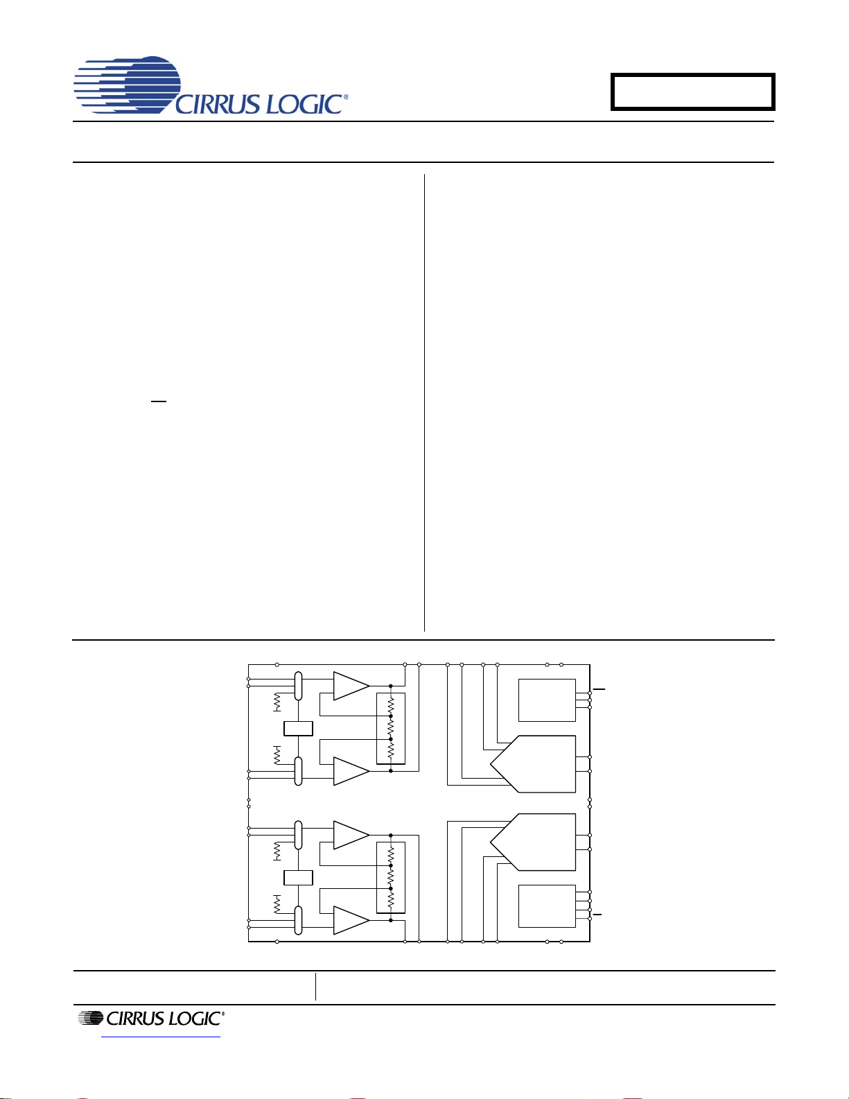
INA1+
INB1+
MUX1
MUX2
INB1-
INA1-
GUARD1
+
-
+
400 Ω 400 Ω
INA2+
INB2+
INB2-
INA2-
+
-
+
400 Ω 400 Ω
Reset, Clock,
and
Synchronization
INR1- VA+
MFLAG1
MCLK
MSYNC
MFLAG2
MDATA2
GAIN1GAIN2
GUARD2 INR2- INR2+
4th Order
Modulator
4
th
Order
Modulator
INF1- INF1+INR1+
RST
SPITM Serial
Interface
SDI
SDO
SCLK
CS
INF2+INF2-OUT2-OUT2+
OUT1+ OUT1-
CS5374
VA-
GND
VD
VREF-VREF+
VA+
VA-
MDATA1
CS5374
Dual High-performance Amplifier &
Features
High Input Impedance Differential Amplifier
• Ultra-low input bias: < 1 pA
• Max signal amplitude: 5 Vpp differential
Fourth Order Delta-Sigma (ΔΣ) Modulator
• Signal Bandwidth: DC to 2 kHz
• Common mode rejection: 110 dB CMRR
Differential Analog Input, Digital ΔΣ Output
• Multiplexed inputs: INA, INB, 800Ω termination
• Selectable Gain: 1x, 2x, 4x, 8x, 16x, 32x, 64x
Excellent Amplifier Noise Performance
•1.5 μVpp between 0.1 Hz and 10 Hz
• 11 nV /
High Modulator Dynamic Range
• 126 dB SNR @ 215 Hz BW (2 ms sampling)
• 123 dB SNR @ 430 Hz BW (1 ms sampling)
Low Total Harmonic Distortion
• –118 dB THD typical (0.000126%)
• –108 dB THD maximum (0.0004%)
Low Power Consumption
• Normal operation: 6.5 mA per channel
• Power down: 15 μA per channel max
Dual Power Supply Configuration
• VA+ = +2.5 V; VA– = –2.5 V; VD = +3.3 V
√Hz from 200 Hz to 2 kHz
Description
The CS5374 combines two marine seismic analog mea surement channels into one 7 mm x 7 mm QFN
package. Each measurement channel consists of a high
input impedance programmable gain differential amplifier that buffers analog signals into a high-performance,
fourth-order ΔΣ modulator. The low-noise ΔΣ modulator
converts the analog signal into a one-bit serial bit stream
suitable for the CS5376A digital filter.
Each amplifier has two sets of external inputs, INA and
INB, to simplify system design as inputs from a hydrophone sensor or the CS4373A test DAC. An internal
800Ω termination can also be selected for noise tests.
Gain settings are binary weighted (1x, 2x, 4x, 8x, 16x,
32x, 64x) and match the CS4373A test DAC output attenuation settings for full-scale testing at all gain ranges.
Both the input multiplexer and gain are set by registers
accessed through a standard SPI™ port.
Each fourth-order ΔΣ modulator has very high dynamic
range combined with low total harmonic distortion and
low power consumption. It converts differential analog
signals from the amplifier to an oversampled ΔΣ serial bit
stream which is decimated by the CS5376A digital filter
to a 24-bit output at the final output word rate.
ORDERING INFORMATION
See page 43.
ΔΣ
Modulator
Preliminary Product Information
http://www.cirrus.com
This document contains information for a new product.
Cirrus Logic reserves the right to modify this product without notice.
Copyright Cirrus Logic, Inc. 2010
(All Rights Reserved)
SEP '10
DS862F2
Page 2

TABLE OF CONTENTS
1. CHARACTERISTICS AND SPECIFICATIONS ....................................................................... 4
SPECIFIED OPERATING CONDITIONS ................................................................................ 4
ABSOLUTE MAXIMUM RATINGS .......................................................................................... 4
THERMAL CHARACTERISTICS ........................... ... .... ... ... ... ....................................... ........... 5
ANALOG CHARACTERISTICS ....................... ................................ ................................ ........ 5
PERFORMANCE SPECIFICATIONS ...................................................................................... 7
CHANNEL PERFORMANCE PLOTS ...................................................................................... 9
DIGITAL CHARACTERISTICS ........................ ................................ ................................ ...... 10
SPI™ INTERFACE TIMING (EXTERNAL MASTER) ............................................................ 12
POWER SUPPLY CHARACTERISTICS ......................... ...................................................... 13
2. GENERAL DESCRIPTION..................................................................................................... 14
3. AMPLIFIER OPERATION ...................................................................................................... 16
3.1 Amplifier Inputs — INA, INB.......................................................................................... 16
3.1.1 Multiplexer Settings — MUX............................................................................... 16
3.1.2 Gain Settings — GAIN........................................................................................ 16
3.2 Amplifier Outputs — OUTR, OUTF............................................................................... 16
3.2.1 Guard Output — GUARD.................................................................................... 16
3.3 Differential Signals . .... ... ... ... .... ... ....................................... ... ...................................... ... 17
4. MODULATOR OPERATION .................................................................................................. 18
4.1 Modulator Anti-Alias Filter............................................................................................. 18
4.2 Modulator Inputs — INR, INF........................................................................................ 19
4.2.1 Modulator Input Impedance ................................................................................ 19
4.2.2 Modulator Idle Tones — OFST.............. .... ... ... ... .... ... ...................................... ... 19
4.3 Modulator Output — MDATA ........................................................................................ 19
4.3.1 Modulator One’s Density............................... ... ... .... ... ...................................... ... 19
4.3.2 Decimated 24-bit Output..................................................................................... 19
4.4 Modulator Stability — MFLAG.... ... ... ....................................... ...................................... 20
4.5 Modulator Clock Input — MCLK.................................................................................... 20
4.6 Modulator Synchronization — MSYNC......................................................................... 20
5. SPI
6. POWER MODES .................................................................................................................... 29
7. VOLTAGE REFERENCE ....................................................................................................... 30
8. POWER SUPPLIES .............................................................................................................. 32
TM
SERIAL PORT ............................................................................................................. 21
5.1 SPI Pin Descriptions ..................................................................................................... 21
5.2 SPI Serial Transactions................................................................................................. 21
5.3 SPI Registers ................................................................................................................23
5.3.1 VERSION — 0x00............................................................................................... 23
5.3.2 AMP1CFG — 0x01 ............................................................................................. 23
5.3.3 AMP2CFG — 0x02 ............................................................................................. 23
5.3.4 ADCCFG — 0x03................................................................................................ 24
5.3.5 PWRCFG — 0x04............................................................................................... 24
5.4 Example: CS5374 Configuration by an External SPI Master........................................ 24
5.5 Example: CS5374 Configuration by the CS5376A SPI 2 Port ...................................... 25
5.5.1 CS5376A SPI 1 Transactions ............................................................................. 25
6.1 Normal Operation.......................................................................................................... 29
6.2 Power Down, MCLK Enabled........................................................................................ 29
6.3 Power Down, MCLK Disabled....................................................................................... 29
7.1 VREF Power Supply ..................................................................................................... 30
7.2 VREF RC Filter ............................................................................................................. 30
7.3 VREF PCB Routing....................................................................................................... 30
7.4 VREF Input Impedance................................................................................................. 30
7.5 VREF Accuracy............................................................................................................. 31
8.1 Analog Power Supplies................................................................................................. 32
8.2 Digital Power Supply..................................................................................................... 32
8.3 Power Supply Bypassing .............................................. .... ... ...................................... ... 32
CS5374
CS5374
2
Page 3

8.4 PCB Layers and Routing............................................................................................... 33
8.5 Power Supply Rejection............................................................................. ................... 33
8.6 SCR Latch-up Considerations....................................................................................... 33
8.7 DC-DC Converters........................................................................................................ 33
9. SPI
10. PIN DESCRIPTIONS ............................................................................................................. 40
11. PACKAGE DIMENSIONS ...................................................................................................... 42
12. ORDERING INFORMATION ................................................................................................. 43
13. ENVIRONMENTAL, MANUFACTURING, & HANDLING INFORMATION ........................... 43
14. REVISION HISTORY ............................................................................................................44
TM
REGISTER SUMMARY................................................................................................ 34
9.1 VERSION: 0x00 ................................................................... ... ...................................... 35
9.2 AMP1CFG: 0x01........................................................................................................... 36
9.3 AMP2CFG: 0x02........................................................................................................... 37
9.4 ADCCFG: 0x03 ............................................................................................................. 38
9.5 PWRCFG: 0x04 ............................................................................................................ 38
LIST OF FIGURES
Figure 1. External Anti-alias Filter Components.............................................................................. 6
Figure 2. CS5374 Amplifier Noise Performance........... ... .... ........................................................... 7
Figure 3. CS5374 Noise Performance (1x Gain) ........................................................................... 9
Figure 4. CS5374 + CS4373A Test DAC Dynamic Performance ................................................... 9
Figure 5. Digital Rise and Fall Times SYNC from external system............................................... 10
Figure 6. System Synchronization Diagram.................................................................................. 10
Figure 7. MCLK / MSYNC Timing Detail....................................................................................... 11
Figure 8. SDI Write Timing in SPI Slave Mode ............................................................................. 12
Figure 9. SDO Read Timing in SPI Slave Mode........................................................................... 12
Figure 10. CS5374 System Block Diagram................................................................................... 14
Figure 11. CS5374 Connection Diagram...................................................................................... 15
Figure 12. CS5374 to CS5376A Digital Interface.......................................................................... 15
Figure 13. CS5374 Amplifier Block Diagram................................................................................. 16
Figure 14. CS5374 Modulator Block Diagram............................................................................... 18
Figure 15. SPI Interface Block Diagram........................................................................................ 21
Figure 16. CS5374 (Slave) Serial Transactions with CS5376A (Master)...................................... 22
Figure 17. Power Mode Diagram.................................................................................................. 29
Figure 18. Voltage Reference Circuit............................................................................................30
Figure 19. Power Supply Diagram................................................................................................ 32
Figure 20. Hardware Version ID Register VERSION................................. ... .... ............................ 35
Figure 21. Amplifier 1 Configuration Register AMP1CFG............................................................. 36
Figure 22. Amplifier 2 Configuration Register AMP2CFG............................................................. 37
Figure 23. Modulator 1 & 2 Configuration Register ADCCFG....................................................... 38
Figure 24. Power Configuration Register PWRCFG..................................................................... 39
CS5374
CS5374
LIST OF TABLES
Table 1. 24-bit Output Coding ...................................................................................................... 20
Table 2. SPI Configuration Registers ...........................................................................................23
Table 3. Digital Selections for Gain and Input Mux Control ................................... ... .... ............... 23
Table 4. Example SPI Transactions to Write and Read the CS5374 Configuration Registers .... 24
Table 5. Example CS5376A SPI 1 Transactions to Write and Read the GPCFG0 Register ....... 25
Table 6. Example CS5376A SPI 1 Transactions to Write the CS5374 AMP1CFG Register .......26
Table 7. Example CS5376A SPI 1 Transactions to Write AMP2CFG and ADCCFG .................. 27
Table 8. Example CS5376A SPI 1 Transactions to Write the CS5374 PWRCFG Register ......... 28
3
Page 4
CS5374
CS5374
1. CHARACTERISTICS AND SPECIFICATIONS
• Min/Max characteristics and specifications are guaranteed over the Specified Operating Conditions.
• Typical performance characteristics and specifications are derived from measurements taken at nominal supply voltages and T
= 25°C.
A
• GND = 0 V, all voltages with respect to 0 V.
• Device connected as shown in Figure 11 and Figure 12 unless otherwise noted.
SPECIFIED OPERATING CONDITIONS
Parameter Symbol Min Nom Max Unit
Bipolar Power Supplies
Positive Analog +
Negative Analog (Note 1) +
Positive Digital +
Voltage Reference
[VREF+] - [VREF-] (Note 2, 3) VREF - 2.500 - V
VREF- (Note 4)VREF- - VA- - V
Thermal
Ambient Operating Temperature -CNZ T
2% VA+ 2.45 2.50 2.55 V
2% VA- -2.45 -2.50 -2.55 V
3% VD 3.20 3.30 3.40 V
A
-10 25 70 °C
Notes: 1. VA- must always be the most-negative input voltage to avoid potential SCR latch-up conditions.
2. By design, a 2.500 V voltage reference input results in the best signal-to-noise performance.
3. Channel-to-channel gain accuracy is directly proportional to the voltage reference absolute accuracy.
4. VREF inputs must satisfy: VA- ≤ VREF- < VREF+ ≤ VA+.
ABSOLUTE MAXIMUM RATINGS
Parameter Symbol Min Max Unit
DC Power Supplies Positive Analog
Negative Analog
Digital
Analog Supply Differential [(VA+) - (VA-)] VA
Digital Supply Differential [(VD) - (VA-)] VD
Input Current, Any Pin Except Supplies (Note 5, 6)I
Input Current, Power Supplies (Note 5)I
Output Current (Note 5)I
Power Dissipation PD - 500 mW
Analog Input Voltages V
Digital Input Voltages V
Storage Temperature Range T
WARNING: Operation at or beyond these limits may result in permanent damage to the device.
Normal operation is not guaranteed at these extremes.
Notes: 5. Transient currents up to 100mA will not cause SCR latch-up.
6. Includes continuous over-voltage conditions on the analog input pins.
VA+
VA-
VD
DIFF
DIFF
IN
PWR
OUT
INA
IND
STG
-0.3
-6.8
-0.3
-6.8V
-6.8V
-+10 mA
-+50 mA
-+25 mA
(VA-)-0.5 (VA+)+0.5 V
-0.5 (VD)+0.5 V
-65 150 °C
6.8
0.3
6.8
V
V
V
4
Page 5
CS5374
CS5374
THERMAL CHARACTERISTICS
Parameter Symbol Min Typ Max Unit
Ambient Operating Temperature T
Storage Temperature Range T
Allowable Junction Temperature T
Junction to Ambient Thermal Impedance (4-layer PCB) θ
A
STR
JCT
JA
-10 - 70 °C
-65 - 150 °C
--125°C
-26-°C/W
ANALOG CHARACTERISTICS
Parameter Symbol Min Typ Max Unit
Amplifier Inputs
Signal Frequencies BW DC - 2000 Hz
Differential Gain GAIN x1 - x 64
Common Mode Gain (Note 7) GAIN
Common Mode Voltage V
Voltage Range (Signal + Vcm) x1
CM
cm
V
IN
x2 - x64
Full Scale Differential Input x1
x2
x4
x8
V
INFS
x16
x32
x64
Differential Input Impedance Z
Common Mode Input Impedance Z
Input Bias Current I
INDIFF
INCM
IN
Amplifier Outputs
Full Scale Output, Differential V
Output Voltage Range (Signal + Vcm) V
Output Impedance (Note 8)Z
Output Impedance Drift (Note 8)Z
Output Current I
Load Capacitance C
OUT
RNG
OUT
TC
OUT
L
Guard Outputs
Guard Output Voltage V
Guard Output Impedance (Note 8)ZG
Guard Output Current IG
Guard Load Capacitance CG
GUARD
OUT
OUT
L
-x1-
(VA-)+2.5
-
(VA-)+0.7
(VA-)+0.7
-
-
-
-
-
-
-
-
-
-
-
-
-
-
-
-
-V
(VA+)-1.25
(VA+)-1.75
5
2.5
1.25
625
312.5
156.25
78.125
V
V
V
mV
mV
mV
mV
-1, 20- TΩ, pF
- 0.5, 40 - TΩ, pF
-140pA
--5V
(VA-)+0.5
-
(VA+)-0.5
-40- Ω
-0.38- Ω/°C
--+25 mA
--100nF
-Vcm-V
-500- Ω
--40μA
--100pF
V
pp
pp
pp
pp
pp
pp
pp
pp
V
Notes: 7. Common mode signals pass thro ug h th e diff er en tial amplifier architecture and are rejected by the
modulator CMRR.
8. Output impedance characteristics are approximate and can vary up to ±30% depending on process
parameters.
5
Page 6
CS5374
MODULATOR
INR+
INF+
INFINR-
20nF
C0G
20nF
C0G
680
AMPLIFIER
OUT+
OUT-
680
680
680
CS5374
Figure 1. External Anti-alias Filter Components
CS5374
ANALOG CHARACTERISTICS (CONT.)
Parameter Symbol Min Typ Max Unit
Modulator Inputs
Input Signal Frequencies (Note 9) V
Full-scale Differential AC Input V
Full-scale Differential DC Input V
Input Common Mode Voltage V
Input Voltage Range (V
±Signal) V
cm
Differential Input Impedance INR±
INF±
Single-ended Input Impedance INR±
INF±
External Anti-alias Filter Series Resistance
(Note 10) Differential Capacitance
RNG
ZDIF
ZDIF
ZSE
ZSE
R
C
DIFF
BW
AC
DC
CM
INR
INF
INR
INF
AA
VREF Inputs
[VREF+] - [VREF-] (Note 2, 3) VREF - 2.500 - V
VREF- (Note 4)VREF- - VA- - V
VREF Input Current VREF
VREF Input Noise (Note 11)VREF
II
IN
DC - 2000 Hz
--5V
-2.5 - 2.5 V
(VA-)+2.5
-
(VA-)+0.7
-
-
-
-
-
-
-
20
1
40
2
680
20
-V
(VA+)-1.25
-
-
-
-
-
-
pp
DC
V
kΩ
MΩ
kΩ
MΩ
Ω
nF
-120- µA
--1µV
rms
Notes: 9. The upper bandwidth limit is determined by the selected digital filter cut-off frequency.
10. Anti-alias capacitors are discrete exte rnal components and must be of good quality (C0G, NPO, po ly).
Poor-quality capacitors will degrade total harmonic distortion (THD) performance. See Figure 1 for
external anti-alias filter connections.
11. Maximum integrated noise over the mea surement bandwidth for the voltage reference device attached
to the VREF inputs.
6
Page 7
CS5374
nV/ Hz
fA/ Hz
0
5
10
15
20
0 200 400 600 800 1000 1200 1400 1600 1800 2000
Frequency (Hz)
CS5374 Amplifier In-Band Noise
Noise Density (nV/rtHz)
0
100
200
300
400
0.1
1 10 100 1k
Frequency (Hz)
CS5374 Amplifier Wide Band Noise
Noise Density (nV/rtHz)
10k 100k 1M
Figure 2. CS5374 Amplifier Noise Performance
PERFORMANCE SPECIFICATIONS
Parameter Symbol Min Typ Max Unit
Amplifier Noise
Voltage Noise f
Voltage Noise Density f0 = 200 Hz to 2 kHz VN
Current Noise Density IN
Channel Dynamic Range
Dynamic Range (1/4 ms) DC to 1720 Hz
(1x Gain, Multiple OWRs) (1/2 ms) DC to 860 Hz
(Note 9, 12) (1ms)DCto 430Hz
Dynamic Range 1x
(Multiple Gains, 1 ms OWR) 2x
(Note 9, 12)3x
Channel Distortion
Total Harmonic Distortion 1x
(Note 13)2x
= 0.1 Hz to 10 Hz VN
0
(2 ms) DC to 215 Hz
(4 ms) DC to 108 Hz
(8 ms) DC to 54 Hz
(16 ms) DC to 27 Hz
8x
16x
32x
64x
4x
8x
16x
32x
64x
PP
D
D
-1.5 3 μV
-11 14
-20 -
SNR -
-
121
-
-
-
-
SNR 121
-
-
-
-
-
-
-
-
-
THD
-
-
-
-
105
120
123
126
129
131
135
123
122
120
116
111
105
98
-118
-119
-119
-119
-118
-115
-112
-
-
-
-
-
-
-
-
-
-
-
-
-
-
-108
-
-
-
-
-
-
CS5374
pp
dB
dB
dB
dB
dB
dB
dB
dB
dB
dB
dB
dB
dB
dB
dB
dB
dB
dB
dB
dB
dB
Notes: 12. Dynamic Range defined as 20 log [(RMS full scale) / (RMS idle noise)] where idle noise is measured
with the amplifier input terminated. Dynamic Range is dominated by high-frequency quantization noise
at the 1/4 ms rate and amplifier noise at high gain.
13. Tested with a 31.25 Hz sine wave at 1 ms sampling rate and -1dB amplitude.
7
Page 8
CS5374
CS5374
PERFORMANCE SPECIFICATIONS (CONT.)
CS5374
Parameter Symbol
Channel Gain Accuracy
Channel Gain, Offset Corrected (Note 3, 14)GAIN
Absolute Gain Accuracy (Note 3, 15)GAIN
Relative Gain Accuracy 2x
(Note 16)4x
8x
GAIN
16x
32x
64x
Gain Drift (Note 17) GAIN
LSB
ABS
REL
TC
-6101194
0xA2E736
-±1+2%
-0.3
-
-
-
-
-
-25-ppm/°C
-
-
-0.1
-0.1
0.1
0.4
0.4
0.3
6101194
0x5D18CA
0.1
-
-
-
-
-
Channel Offset Accuracy
Amplifier Offset Voltage, Input Referred (Note 18)OFST
Amplifier Offset Drift, Input Referred (Note 17)OFST
Modulator Offset Voltage, Differential (OFST
Modulator Offset Voltage, Channel 1 (OFST
Modulator Offset Voltage, Channel 2 (OFST
=1) OFST
=0) OFST
=0) OFST
Modulator Offset Drift (Note 17)OFST
Offset After Calibration (Note 19)OFST
Offset Calibration Range (Note 20)OFST
AMP
ATC
MOD
MOD1
MOD2
MTC
CAL
RNG
- ±250 ±750 µV
-0.3-µV/°C
-±1- mV
--60- mV
--35- mV
-1-µV/°C
-±1- μV
-100- %FS
Channel CMRR and Crosstalk
Common Mode Rejection Ratio CMRR - 110 - dB
Crosstalk, Amplifier Multiplexed Inputs CXT
Crosstalk, Channel-to-Channel CXT
MI
CC
--130- dB
--130- dB
UnitMin Typ Max
LSB
LSB
%
%
%
%
%
%
Notes: 14. Channel Gain is the nominal full-scale 24-bit output code from the CS5376A digital filter for a 5 VPP
differential signal into the CS5374 analog inputs at 1x gain. Value is offset corrected.
15. Absolute gain accuracy tests the matching of 1x gain across multiple CS5374 channels in a system.
16. Relative gain accuracy tests the tra cking of 2x, 4x, 8x, 16x, 32x, 64x gain re lative to 1x gain on a single
CS5374 channel.
17. Specification is for the parameter over the specified temperature range and is for the CS5374 device
only. It does not include the effects of external components.
18. Offset voltage is tested with the amplifier inputs connected to the internal 800 Ω termination.
19. The offset after calibration specification is measured from the digitally calibrated output codes of the
CS5376A digital filter.
20. Offset calibration is performed in the CS5376A digital filter and includes the full-scale sig nal range.
8
Page 9
CHANNEL PERFORMANCE PLOTS
Figure 3. CS5374 Noise Performance (1x Gain)
Figure 4. CS5374 + CS4373A Test DAC Dynamic Performance
CS5374
CS5374
9
Page 10
CS5374
0.9 * VD
0.1 * VD
t
fall
t
rise
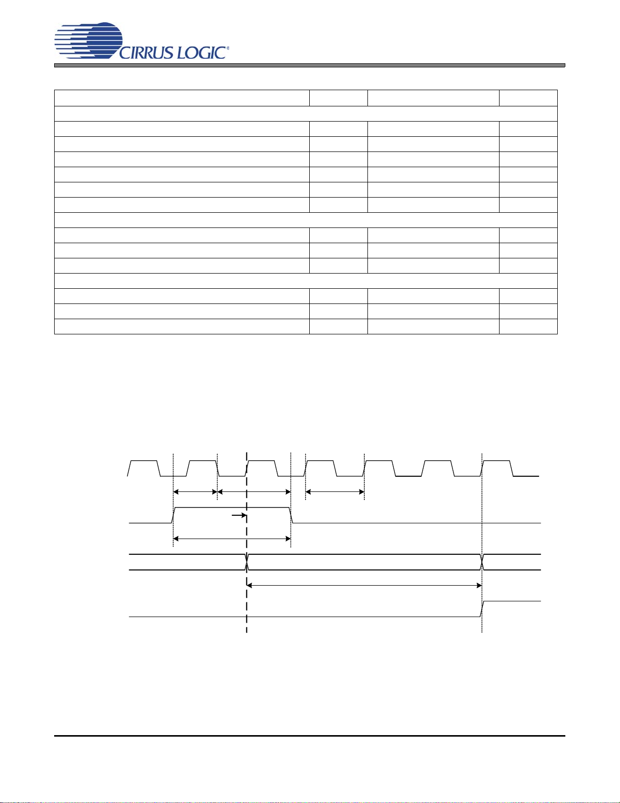
Figure 5. Digital Rise and Fall Times SYNC from external system.
MCLK
MSYNC
t
MDATA
TDATA
0
SYNC
MFLAG
Figure 6. System Synchronization Diagram
SYNC from External. MCLK, MSYNC, TDATA from CS5376A. MDATA, MFLAG from CS5374.
DIGITAL CHARACTERISTICS
Parameter Symbol Min Typ Max Unit
Digital Inputs
High-level Input Voltage (Note 21)V
Low-level Input Voltage (Note 21)V
Input Leakage Current I
Digital Input Capacitance C
Input Rise Times Except MCLK t
Input Fall Times Except MCLK t
Digital Outputs
High-level Output Voltage, I
Low-level Output Voltage, I
=-40μAV
out
=40μAV
out
High-Z Leakage Current I
Digital Output Capacitance C
Output Rise Times (Note 22) t
Output Fall Times (Note 22) t
IH
IL
IN
IN
RISE
FALL
OH
OL
OZ
OUT
RISE
FALL
CS5374
0.6*VD - VD V
0.0 - 0.8 V
-±1±10μA
-9- pF
--100ns
--100ns
VD - 0.3 - - V
--0.3V
-±1±10μA
-9- pF
--100ns
--100ns
Notes: 21. Device is intended to be driven with CMOS logic levels.
22. Guaranteed by design and/or characterization.
10
Page 11
CS5374
MCLK
MSYNC
t
0
t
MSS
1 / f
MCLK
t
MSYNC
t
MSH
MDATA
MFLAG
1 / f
MDATA
Figure 7. MCLK / MSYNC Timing Detail
DIGITAL CHARACTERISTICS (CONT.)
Parameter Symbol Min Typ Max Unit
Master Clock Input
MCLK Frequency (Note 23)f
MCLK Duty Cycle MCLK
MCLK Rise Time t
MCLK Fall Time t
MCLK Jitter (in-band or aliased in-band) MCLK
MCLK Jitter (out-of-band) MCLK
Master Sync Input
MSYNC Setup Time to MCLK Falling (Note 24)t
MSYNC Period (Note 24)t
MSYNC Hold Time after MCLK Falling (Note 24)t
MDATA Output
MDATA Output Bit Rate f
MDATA Output One’s Density Range (Note 22)MDAT
Full-scale Output Code, Offset Corrected (Note 25)MDAT
MCLK
DTC
RISE
FALL
IBJ
OBJ
MSS
MSYNC
MSH
MDATA
1D
FS
CS5374
- 2.048 - MHz
40 - 60 %
- - 50 ns
- - 50 ns
--300ps
--1ns
20 366 - ns
40 976 - ns
20 610 - ns
-512-kbits/s
14 - 86 %
0xA2E736 - 0x5D18CA
Notes: 23. MCLK is generated by the CS5376A digital filter. If MCLK is disabl ed, the CS5374 device automatically
enters a power-down state. See Power Supply Characteristics for typical power-down timing.
24. MSYNC is generated by the CS5376A digital filter and is latched by CS5374 on MCLK falling edge,
synchronization instant (t
) is on the next MCLK rising edge.
0
25. Decimated, filtered, and offset-corrected 24-bit output word from the CS5376A digital filter.
11
Page 12
CS5374
MSB MSB - 1 LSB
t
6
t
5
t
4
t
3
t
2
t
1
CS
SDI
SCK
Figure 8. SDI Write Timing in SPI Slave Mode
MSB MSB - 1 LSB
t
9
t
8
t
7
CS
SDO
SCK
t
10
Figure 9. SDO Read Timing in SPI Slave Mode
SPI™ INTERFACE TIMING (EXTERNAL MASTER)
Parameter Symbol Min Typ Max Unit
SDI Write Timing
CS
Enable to Valid Latch Clock t
Data Set-up Time Prior to SCK Rising t
Data Hold Time After SCK Rising t
SCK High Time t
SCK Low Time t
SCK Falling Prior to CS
Disable t
1
2
3
4
5
6
SDO Read Timing
SCK Falling to New Data Bit t
SCK High Time t
SCK Low Time t
SCK Falling Hold Time Prior to CS
Disable t
7
8
9
10
CS5374
60 - - ns
60 - - ns
60 - - ns
120 - - ns
120 - - ns
60 - - ns
- - 90 ns
120 - - ns
120 - - ns
60 - - ns
12
Page 13
CS5374
CS5374
POWER SUPPLY CHARACTERISTICS
Parameter Symbol Min Typ Max Unit
Power Supply Current, ch1 + ch2 combined
Analog Power Supply Current (Note 26)I
Digital Power Supply Current (Note 26)I
A
D
Power Supply Current, ch1 or ch2 only
Analog Power Supply Current (Note 26)I
Digital Power Supply Current (Note 26)I
A
D
Power Down Current, MCLK enabled
Analog Power Supply Current (Note 26)I
Digital Power Supply Current (Note 26)I
A
D
Power Down Current, MCLK disabled
Analog Power Supply Current (Note 26)I
Digital Power Supply Current (Note 26)I
Power Down Timing (after MCLK disabled) (Note 22)PD
A
D
TC
Power Supply Rejection
Power Supply Rejection Ratio (Note 22)PSRR - 100 - dB
-1316mA
-50100μA
-6.58 mA
-2550 μA
- 150 250 μA
-1075 μA
-215μA
-115μA
-40- μS
Notes: 26. All outputs unloaded. Digital inputs forced to VD or GND respectively. Amplifier inputs connected to the
800 Ω internal termination.
13
Page 14
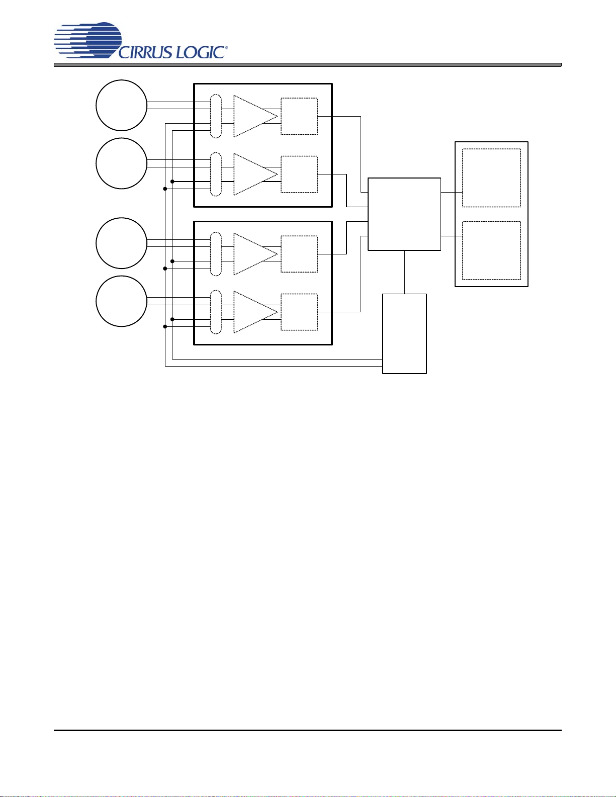
CS5374
Hydrophone
Sensor
Hydrophone
Sensor
Hydrophone
Sensor
Hydrophone
Sensor
DS
Modulator
Digital Filter
CS5376A
Test
DAC
Microcontroller
or
Configuration
EEPROM
System
Telemetry
AMP
CS4373A
CS5374
DS
Modulator
AMP
M
U
X
DS
Modulator
AMP
M
U
X
CS5374
DS
Modulator
AMP
M
U
X
M
U
X
Figure 10. CS5374 System Block Diagram
CS5374
2. GENERAL DESCRIPTION
The CS5374 combines two marine seismic analog
measurement channels into one 7 mm x 7 mm QFN
package. Each measurement channel consists of a
high input impedance programmable gain differential amplifier that buffers analog signals into a
high-performance, fourth-order ΔΣ modulator. The
low-noise ΔΣ modulator converts the analog signal
into a one-bit serial bit stream suitable for the
CS5376A digital filter.
Each amplifier has two sets of external inputs, INA
and INB, to simplify system design as inputs from
a hydrophone sensor or the CS4373A test DAC. An
internal 800 Ω termination can also be selected for
noise tests. Gain settings are binary weighted (1x,
2x, 4x, 8x, 16x, 32x, 64x) and match the CS4373A
test DAC output attenuation settings for full-scale
testing at all gain ranges. Both the input multiplex-
er and gain are set by registers accessed through a
standard SPI™ port.
Each fourth-order ΔΣ modulator has very high dynamic range combined with low total harmonic distortion and low power consumption. It converts
differential analog signals from the amplifier to an
oversampled ΔΣ serial bit stream which is decimated by the CS5376A digital filter to a 24-bit output
at the final output word rate.
Figure 10 shows the system-level architecture of a
4-channel acquisition system using two CS5374,
one CS5376A digital filter and one CS4373A test
DAC.
Figure 11 and Figure 12
grams for the CS5374 device when connected to
shows connection dia-
the CS5376A digital filter.
14
Page 15

CS5374
Figure 11. CS5374 Connection Diagram
A
INA1+
INA1-
MUX1
MUX2
INB1-
INB1+
GUAR D1
+
-
+
400 Ω 400 Ω
INB2+
INB2-
INA2-
INA2+
+
-
-
+
400 Ω 400 Ω
Reset, Clock, and
Synchronization
INR1-
VA+
MFLAG1
MDATA1
MCLK
MSYNC
MFLAG2
MDATA2
GAIN1GAIN2
GUARD2
INR2-
INR2+
4th Order
ΔΣ Modulato r
4
th
Order
ΔΣ Modulato r
INF1-
INF1+ INR1+
RST
SPITM Serial
Communications
Interface
SDI
SDO
SCLK
CS
INF2+
INF2-
OUT2-OUT2+
OUT1 + OUT1 -
CS5374
VA-
GND
VD+
VREF-VREF+
VA+
VA-
Hydrophone
Sensor
Hydrophone
Sensor
VA-
0.1
VA+
0.1 μF
μF
Test
DAC
CS4373A
0.02
C0G
0.02
C0G
680
680
680
680
μF μ
Ω
Ω
Ω
Ω
F
0.02
C0G
0.02
C0G
680
680
680
680
μF μ
Ω
Ω
Ω
F
Ω
VA-
0.1
VA+
0.1
μF
μF
0.01μF
2.5V
Precision
Voltage
Reference
To CS5376A
Digital Control
Figure 12. CS5374 to CS5376A Digital Interface
Reset, Clock, and
Synchronization
MFLAG1
MDATA1
MCLK
MSYNC
MFLAG2
MDATA2
4th Order
ΔΣ Modulator
4
th
Order
ΔΣ Modulator
RST
SPITM Serial
Communications
Interface
SDI
SDO
SCLK
CS
CS5374
MSYNC
MCLK
Clock an d
Synchronization
Modulator Data
Interface
SPI 2
Serial Pe riph eral
Interface 2
RESET
MFLAG1
MDATA1
MFLAG2
MDATA2
SI1
SO
SCK2
CS0
CS5376A
EXTERN AL R ESET
CONTROLLER
CS5374
15
Page 16

3. AMPLIFIER OPERATION
INA1+
INB1+
MUX1
INB1-
INA1-
GUARD1
+
-
+
400 Ω 400 Ω
GAIN1
OUT1+ OUT1-
Figure 13. CS5374 Amplifier Block Diagram
CS5374
CS5374
The CS5374 high-impedance, low-noise CMOS
differential input, differential output amplifiers are
optimized for precision analog signals between DC
and 2 kHz. They have multiplexed inputs and programmable gains of 1x, 2x, 4x, 8x, 16x, 32x, and
64x. The performance of this amplifier makes it
ideal for low-frequency, high-dynamic-range applications requiring low distortion and minimal
power consumption.
3.1 Amplifier Inputs — INA, INB
The amplifier analog inputs are designed for highimpedance differential hydrophone sensors and so
have very low input bias below 1 pA.
3.1.1 Multiplexer Settings — MUX
Input multiplexing simplifies system connections
by providing separate inputs for a sensor and test
DAC (INA, INB) as well as an internal termination
for noise tests. The multiplexer determines which
input is connected to the amplifier, and is set
through internal configuration registers accessed
through the SPI port, see the “SPI
mary” on page 34 for more information.
Although a mux selection is provided to enable the
INA and INB switches simultaneously, significant
current should not be driven through them in this
16
TM
Register Sum-
mode. The CS5374 mux switches will maintain
good linearity only with minimal signal current.
3.1.2 Gain Settings — GAIN
The CS5374 supports gain ranges of 1x, 2x, 4,x 8x,
16x, 32x, and 64x. Amplifier gain is selected using
internal configuration registers accessed through
the SPI port, see the “SPITM Register Summary”
on page 34 for more information.
3.2 Amplifier Outputs — OUTR, OUTF
The amplifier analog outputs are externally separated into rough / fine charge signals to connect
into the modulator inputs. Each differential output
requires two series resistors and a differential capacitor to create the modulator anti-alias RC filter.
3.2.1 Guard Output — GUARD
The GUARD pin outputs the common mode voltage of the selected analog signal input. It can be
used to drive the cable shield between a high-impedance sensor and the amplifier inputs. Driving
the cable shield with the analog signal common
mode voltage minimizes leakage and improves signal integrity from high-impedance sensors.
The GUARD output is defined as the midpoint
voltage between the + and – halves of the currently
Page 17

selected differential input signal, and will vary as
the signal common mode varies. The GUARD output will not drive a significant load, as it can only
provide a shielding voltage.
3.3 Differential Signals
Analog signals into and out of the amplifiers are
differential, consisting of two halves with equal but
opposite magnitude varying about a common mode
voltage.
A full-scale 5 Vpp differential signal centered on a
–0.15 V common mode can have:
SIG+ = –0.15 V + 1.25 V = 1.1 V
SIG– = –0.15 V – 1.25 V = –1.4 V
SIG+ is +2.5 V relative to SIG-
CS5374
CS5374
For the reverse case:
SIG+ = –0.15 V – 1.25 V = –1.4 V
SIG– = –0.15 V + 1.25 V = 1.1 V
SIG+ is –2.5 V relative to SIG-
The total swing for SIG+ relative to SIG– is
(+2.5 V) – (–2.5 V) = 5 Vpp. A similar calculation
can be done for SIG– relative to SIG+. Note that a
5Vpp differential signal centered on a –0.15 V
common mode voltage never exceeds 1.1 V and
never drops below –1.4 V on either half of the signal.
By definition, differential voltages are to be measured with respect to the opposite half, not relative
to ground. A multi-meter differentially measuring
between SIG+ and SIG– in the above example
would properly read 1.767 V
, or 5 Vpp.
rms
17
Page 18

4. MODULATOR OPERATION
Reset, Clock,
and
Synchronization
INR1- VREF-
MFLAG1
MCLK
MSYNC
4th Order
Modulator
INF1- INF1+INR1+
RST
VREF+
MDATA1
Figure 14. CS5374 Modulator Block Diagram
• MCLK Frequency = 2.048 MHz
• Sampling Frequency = MCLK / 4 = 512 kHz
• –3 dB Filter Corner = Sampling Freq / 64 = 8 kHz
• RC filter = 1 / [ 2π x(2xR
series
)xC
diff
] ~ 8 kHz
CS5374
CS5374
The CS5374 modulators are fourth-order ΔΣ type
optimized for extremely high-resolution measurement of signals between DC and 2000 Hz. When
combined with the internal differential amplifiers,
the CS4373A test DAC and CS5376A digital filter,
a small, low-power, self-testing, high-accuracy,
multi-channel measurement system results.
The modulators have high dynamic range and low
total harmonic distortion with very low power consumption. They are optimized for extremely highresolution measurement of 5 V
ential signals. They convert analog input signals
from the differential amplifiers to an oversampled
serial bit stream which is then passed to the digital
filter.
The companion CS5376A digital filter generates
the clock and synchronization inputs for the modulators while receiving the one-bit data and overrange flag outputs. The digital filter decimates the
modulator’s oversampled output bit stream to a
high-resolution, 24-bit output at the final selected
output word rate.
4.1 Modulator Anti-Alias Filter
The modulator inputs are required to be bandwidth
limited to ensure modulator loop stability and pre-
or smaller differ-
p-p
vent high-frequency signals from aliasing into the
measurement bandwidth. The use of simple, single-pole, differential, low-pass RC filters across
the INR± and INF± inputs ensures high-frequency
signals are rejected before they can alias into the
measurement bandwidth.
The approximate –3 dB corner of the input antialias filter is nominally set to the internal analog
sampling rate divided by 64, which itself is a division by 4 of the MCLK rate.
Figure 1 on page 6 illustrates the CS5374 amplifier-to-modulator analog connections with input
anti-alias filter components. Filter components on
the rough and fine pins should be identical values
for optimum performance, with the capacitor values a minimum of 0.02 μF. The rough input can use
either X7R or C0G-type capacitors, while the fine
input requires C0G-type capacitors for optimal linearity. Using X7R-type capacitors on the fine analog inputs will significantly degrade total harmonic
distortion performance.
18
Page 19

CS5374
• MCLK = 2.048 MHz
• INR± Internal Input Capacitor = 20 pF
• Impedance = [1 / (2.048 MHz * 20 pF)] = 24 kΩ
CS5374
4.2 Modulator Inputs — INR, INF
The modulator analog inputs are separated into differential rough and fine signals (INR±, INF±) to
maximize sampling accuracy. The positive half of
the differential input signal is connected to INR+
and INF+, while the negative half is attached to
INF– and INR–. The INR± pins are switched-capacitor ‘rough charge’ inputs that pre-charge the
internal analog sampling capacitor before it is connected to the INF± fine input pins.
4.2.1 Modulator Input Impedance
The modulator inputs have a dynamic switched-capacitor architecture and so have a rough charge input impedance that is inversely proportional to the
input master clock frequency and the input capacitor size, [1 / (f · C)].
Internal to the modulator, the rough inputs (INR±)
pre-charge the sampling capacitor used by the fine
inputs (INF±), therefore the input current to the
fine inputs is typically very low and the effective
input impedance is an order of magnitude above
the impedance of the rough inputs.
4.2.2 Modulator Idle Tones — OFST
The modulators are delta-sigma-type and so can
produce “idle tones” in the measurement bandwidth when the differential input signal is a steadystate DC signal near mid-scale. Idle tones result
from low-frequency patterns in the output data
stream and appear in the measurement spectrum as
small tones about -135 dB down from full scale.
By default the OFST bit in the ADCCFG register is
low and idle tones are eliminated within the modulator by adding –60 mV (channel 1) and –35 mV
(channel 2) of internal differential offset during
conversion to push idle tones out of the measurement bandwidth. Care should be taken to ensure
external offset voltages do not negate the internally
added differential offset, or idle tones will reappear.
4.3 Modulator Output — MDATA
The CS5374 modulators are designed to operate
with the CS5376A digital filter. The digital filter
generates the modulator clock and synchronization
signals (MCLK and MSYNC) while receiving
back the modulator one-bit ΔΣ conversion data and
over-range flag (MDATA and MFLAG).
4.3.1 Modulator One’s Density
During normal operation the CS5374 modulators
output a ΔΣ serial bit stream to the MDATA pin,
with a one’s density proportional to the differential
amplitude of the analog input signal. The output bit
rate from the MDATA output is a divide-by-four of
the input MCLK, and so is nominally 512 kHz.
The MDATA output has a 50% one’s density for a
mid-scale analog input, approximately 86% one’s
density for a positive full-scale analog input, and
approximately 14% one’s density for a negative
full-scale analog input. One’s density of the MDATA output is defined as the ratio of ‘1’ bits to total
bits in the serial bit stream output; i.e. an 86% one’s
density has, on average, a ‘1’ value in 86 of every
100 output data bits.
4.3.2 Decimated 24-bit Output
When the CS5374 modulators operate with the
CS5376A digital filter, the final decimated, 24-bit,
full-scale output code range depends if digital offset correction is enabled. With digital offset correction enabled within the digital filter, amplifier
19
Page 20

CS5374
Table 1. 24-bit Output Coding
Modulator
Differential
Analog Input
Signal
CS5376A Digital Filter
24-Bit Output Code
Offset
Corrected
CH1
–60 mV
Offset
CH2
–35 mV
Offset
> + (VREF+5%) Error Flag Possible
+ VREF 5D18CA 5ADCCE 5BCB22
0 V 000000 FDC404 FEB258
– VREF A2E736 A0AB3A A1998E
> – (VREF+5%) Error Flag Possible
for the CS5374 Modulator and
CS5376A Digital Filter Combination
CS5374
offset and the modulator internal offset are removed from the final conversion result.
4.4 Modulator Stability — MFLAG
The CS5374 ΔΣ modulators have a fourth-order architecture which is conditionally stable and may go
into an oscillatory condition if the analog inputs are
over-ranged more than 5% past either positive or
negative full scale.
If an unstable condition is detected, the modulator
collapses to a first-order system to regain stability
and transitions the MFLAG output low-to-high to
signal an error condition to the CS5376A digital
filter. The MFLAG output connects to a dedicated
input on the digital filter, causing an error flag to be
set in the status byte of the next output data word.
The analog input signal must be reduced to within
the full-scale range for at least 32 MCLK cycles for
the modulator to recover from an oscillatory condition. If the analog input remains over-ranged for an
extended period, the modulator will cycle between
fourth-order and first- order operation and the
MFLAG output will be seen to pulse.
4.5 Modulator Clock Input — MCLK
The CS5376A digital filter generates the master
clock for the CS5374, typically 2.048 MHz, from a
synchronous clock input from the external system.
If MCLK is disabled during operation, the CS5374
will enter a power down state after approximately
40 µS. By default, MCLK is disabled at reset and
is enabled by writing the digital filter CONFIG register.
MCLK must have low jitter to guarantee full analog performance, requiring a crystal- or VCXObased system clock input to the digital filter. Clock
jitter on the digital filter CLK input directly translates to jitter on MCLK.
4.6 Modulator Synchronization — MSYNC
The CS5374 modulators are designed to operate
synchronously with other modulators in a distributed measurement network, so a rising edge on the
MSYNC input resets the internal conversion state
machine to synchronize analog sample timing.
MSYNC is automatically generated by the
CS5376A digital filter after receiving a synchronization signal from the external system, and is chipto-chip accurate within ± 1 MCLK period. The input SYNC signal to the CS5376A digital filter sets
a common reference time t
events, thereby synchronizing analog sampling
across a measurement network. By default,
MSYNC generation is disabled at reset and is enabled by writing the digital filter CONFIG register.
The CS5374 MSYNC input is rising-edge triggered and resets the internal MCLK counter/divider to guarantee synchronous operation with other
system devices. While the MSYNC signal synchronizes the internal operation of the modulators,
by default, it does not synchronize the phase of the
sine wave from the CS4373A test DAC unless enabled in the digital filter TBSCFG register.
for measurement
0
20
Page 21

5. SPITM SERIAL PORT
SCLK
SDO
SDI
Pin Logic
SPI
Figure 15. SPI Interface Block Diagram
Configuration
CS
Registers
Hardware
Serial
RST
CS5374
CS5374
The CS5374 SPI interface is a slave serial port designed to interface with the CS5376A SPI 2 port.
SPI commands from the CS5376A write and read
the CS5374 configuration registers to control hardware operation.
A block diagram of the CS5374 SPI serial interface
is shown in Figure 15, and connections to the
CS5376A SPI 2 port are shown in Figure 12 on
page 15.
5.1 SPI Pin Descriptions
RST — Pin 37
Hardware reset input pin, active low. Defaults the
configuration registers and SPI state machine.
— Pin 25
CS
Chip select input pin, active low.
SCLK — Pin 26
Serial clock input pin. Maximum 4.096 MHz.
SDI — Pin 27
Serial data input pin. Data expected valid on rising
edge of SCLK, transition on falling edge.
SDO — Pin 28
Serial data output pin. Data valid on rising edge of
SCLK, transition on falling edge.
5.2 SPI Serial Transactions
Following reset, master mode serial transactions to
CS5374 assert CS and write serial clocks to SCLK
while writing serial data into SDI or reading serial
data out from SDO.
The CS5374 serial port operates in SPI mode 0
(0,0) and reads or writes configuration registers using standard 8-bit SPI opcodes. Each individual serial transaction is 24-bits long and is generated by
concatenating an 8-bit SPI command opcode, an 8bit register address, and an 8-bit data byte as shown
in Figure 16 on page 22.
The CS5374 SPI state machine requires 24 clocks
with CS
else SPI clock synchronization can be lost. The
CS5376A SPI 2 hardware generates 24 clocks per
transaction and will keep the CS5374 serial port
synchronized at all times. However, if another SPI
master is used and clock synchronization is lost,
two methods are available to recover:
1. Hold CS
shift out any cached SPI data bits. This method retains the existing CS5374 register configuration.
... or ...
2. Apply a hardware reset (toggle RST) and then
rewrite all CS5374 register configuration values.
asserted to fully shift out the SPI data or
high (inactive) and apply 24 clocks to
21
Page 22

CS5374
SCLK
SDI
Figure 16. CS5374 (Slave) Serial Transactions with CS5376A (Master)
CS
SDO
Cycle
SDI
0x02 ADDR DATA
SDO
SDI
SDO
CS5374 SPI Write from CS5376A SPI2
CS5374 SPI Read from CS5376A SPI2
CS
CS
0x03
ADDR
DATA
Instruction Opcode Address Definition
Write 0x02 ADDR[7:0] Write SPI register specified by the address in ADDR.
Read 0x03 ADDR[7:0] Read SPI register specified by the address in ADDR.
MSB LSB
X
612345
MSB LSB612345
18276543
SPI Mode 0 Transaction Details
SPI2CMD[15:8] SPI2CMD[7:0] SPI2DAT[23:16]
SPI2CMD[15:8] SPI2CMD[7:0]
SPI2DAT[23:16]
CS5374
22
Page 23

CS5374
Name Addr. Type # Bits Description
VERSION
0x00 R 8
Device Version ID
AMP1CFG
0x01 R/W 8
Amplifier 1 configuration
AMP2CFG
0x02 R/W 8
Amplifier 2 configuration
ADCCFG
0x03 R/W 8
Modulator 1 & 2 configuration
PWRCFG
0x04 R/W 8
Power configuration
Table 2. SPI Configuration Registers
Gain Selection GAIN2 GAIN1 GAIN0
1x 0 0 0
2x 0 0 1
4x 0 1 0
8x 0 1 1
16x 1 0 0
32x 1 0 1
64x 1 1 0
reserved 1 1 1
Input Selection MUX1 MUX0
800 Ω termination 0 0
INA only 1 0
INB only 0 1
INA + INB 1 1
Table 3. Digital Selections for Gain and Input Mux Control
CS5374
5.3 SPI Registers
The CS5374 SPI registers are 8-bit registers that
control the CS5374 hardware configuration. See
“SPITM Register Summary” on page 34 for detailed bit definitions of the SPI registers listed in
Table 2.
5.3.1 VERSION — 0x00
The VERSION register indicates the hardware revision of the CS5374 device. Read only.
Reset Condition : 0100_0001 (0x41)
Normal Operation : 0100_0001 (0x41)
Power Down Operation : 0100_0001 (0x41)
5.3.2 AMP1CFG — 0x01
The AMP1CFG register controls the amplifier
MUX and GAIN settings for channel 1. It also enables PWDN mode for the channel 1 amplifier plus
enables the GUARD output for channels 1 & 2.
Reset Condition : 0000_0000
Normal Operation : 00MM_0GGG
Power Down Operation : 1000_0000
5.3.3 AMP2CFG — 0x02
The AMP2CFG register controls the amplifier
MUX and GAIN settings for channel 2. It also enables PWDN mode for the channel 2 amplifier.
Reset Condition : 0000_0000
Normal Operation : 00MM_0GGG
Power Down Operation : 1000_0000
23
Page 24

CS5374
SPI Write Transactions
Transaction CS5374 SPI Write Description
01 SI: 02 | 01 | 20
SO: -----------------
Write AMP1CFG register (0x01).
CH1 INA enabled, 1x gain (0x20).
02 SI: 02 | 02 | 20
SO: -----------------
Write AMP2CFG register (0x02).
CH2 INA enabled, 1x gain (0x20).
03 SI: 02 | 03 | 40
SO: -----------------
Write ADCCFG register (0x03).
Normal operation (0x40).
04 SI: 02 | 04 | 8F
SO: -----------------
Write PWRCFG register (0x04).
Normal operation (0x8F).
SPI Read Transactions
Transaction CS5374 SPI Read Description
01 SI: 03 | 00 | 00
SO: ---------- | 41
Read VERSION register (0x00).
Returned data byte on the SO pin.
02 SI: 03 | 01 | 00
SO: ---------- | 20
Read AMP1CFG register (0x01).
Returned data byte on the SO pin.
03 SI: 03 | 02 | 00
SO: ---------- | 20
Read AMP2CFG register (0x02).
Returned data byte on the SO pin.
04 SI: 03 | 03 | 00
SO: ---------- | 40
Read ADCCFG register (0x03).
Returned data byte on the SO pin.
05 SI: 03 | 04 | 00
SO: ---------- | 8F
Read PWRCFG register (0x04).
Returned data byte on the SO pin.
Table 4. Example SPI Transactions to Write and Read the CS5374 Configuration Registers
CS5374
5.3.4 ADCCFG — 0x03
The ADCCFG register can disable modulator
OFST and enable HP mode. It also enables PWDN
mode for the channel 1 & 2 modulators.
Reset Condition : 0000_0000
Normal Operation : 0100_0000
Power Down Operation : 0011_0000
5.3.5 PWRCFG — 0x04
The PWRCFG register can vary bias currents for
the amplifier and modulator to minimize power
consumption.
Reset Condition : 0000_0000
Normal Operation : 1000_1111
Power Down Operation : 0000_0000
5.4 Example: CS5374 Configuration by an External SPI Master
Any SPI master that supports mode 0 (0,0) communication can write and read the configuration registers and control CS5374.
The following example SPI read and write transactions show how to configure the CS5374 for normal operation.
24
Page 25

CS5374
Table 5. Example CS5376A SPI 1 Transactions to Write and Read the GPCFG0 Register
Transaction CS5376A Primary SPI 1 Write Description
01 MOSI: 02 | 03 | 00 00 01 | 00 00 0E | 03 FF FF
MISO: -----------------------------------------------------------
SPI Command : 0x02 : Write
SPI Address : 0x03 : SPICMD
SPICMD : 0x000001 : Write Register
SPIDAT1 : 0x00000E : GPCFG0
SPIDAT2 : 0x03FFFF : CS as Output
02 Delay 1ms, monitor SINT, or poll E2DREQ
See the CS5376A data sheet.
03 MOSI: 02 | 03 | 00 00 02 | 00 00 0E | 00 00 00
MISO: -----------------------------------------------------------
SPI Command : 0x02 : Write
SPI Address : 0x03 : SPICMD
SPICMD : 0x000002: Read Register
SPIDAT1 : 0x00000E : GPCFG0
SPIDAT2 : 0x000000 : Dummy
04 Delay 1ms, monitor SINT, or poll E2DREQ
See the CS5376A data sheet.
05 MOSI: 03 | 06 |---------------|
MISO: -------------| 03 FF FF |
SPI Command : 0x03 : Read
SPI Address : 0x06 : SPIDAT1
SPIDAT1 : 0x03FFFF : GPCFG0
5.5 Example: CS5374 Configuration by the CS5376A SPI 2 Port
CS5374
The CS5374 SPI port was designed to connect to
the CS5376A secondary SPI 2 port as shown in
Figure 12 on page 15.
The CS5376A SPI 2 hardware is controlled by
writing internal digital filter registers SPI2CTRL,
SPI2CMD, and SPI2DAT through a primary SPI 1
port. Chip selects are enabled by writing the
GPCFG0 digital filter register prior to initiating
SPI 2 transactions.
Configuring CS5374 using SPI 2 is more complex
than using an external SPI master, but has the advantage of a single standardized hardware interface
(the primary SPI 1 port on CS5376A) to control
the entire chipset.
5.5.1 CS5376A SPI 1 Transactions
The CS5376A primary SPI 1 port is controlled by
an external SPI master writing commands and data
into the SPI 1 registers (SPICMD, SPIDAT1, and
SPIDAT2). Serial transactions into the CS5376A
primary SPI 1 port start with an SPI opcode, followed by an SPI address, and then data bytes written starting at that SPI address. These data bytes
contain internal commands to write the CS5376A
digital filter registers that control the SPI 2 hardware and enable the chip selects.
A full description of how to write the CS5376A internal digital filter registers using the primary SPI 1
port is described in the CS5376A data sheet.
GPIO Register
Certain GPIO pins on the CS5376A have dual-use
as chip selects for the SPI 2 port. The GPIO0:CS0
and GPIO1:CS1 pins are recommended as dedicated chip selects when connecting two CS5374 devices to the CS5376A SPI 2 port. To operate the
CS0 and CS1 pins as SPI 2 chip selects they must
be programmed as outputs in the GPCFG0 digital
filter register, as shown in Table 5.
SPI2 Registers
Three digital filter registers control the CS5376A
SPI 2 hardware. The SPI2CMD register is 16-bits
wide and contains the first two bytes of the SPI 2
transaction, the SPI opcode and SPI address, in the
lower two bytes (i.e. 0x000204).
25
Page 26

CS5374
Table 6. Example CS5376A SPI 1 Transactions to Write the CS5374 AMP1CFG Register
Transaction CS5376A Primary SPI 1 Write Description
01 MOSI: 02 | 03 | 00 00 01 | 00 00 11 | 00 02 01
MISO: -----------------------------------------------------------
SPI Command : 0x02 : Write
SPI Address : 0x03 : SPICMD
SPICMD : 0x000001 : Write Register
SPIDAT1 : 0x000011 : SPI2CMD
SPIDAT2 : 0x000201 : Write AMP1CFG
02 Delay 1ms, monitor SINT, or poll E2DREQ
See the CS5376A data sheet.
03 MOSI: 02 | 03 | 00 00 01 | 00 00 12 | 20 00 00
MISO: -----------------------------------------------------------
SPI Command : 0x02 : Write
SPI Address : 0x03 : SPICMD
SPICMD : 0x000001: Write Register
SPIDAT1 : 0x000012 : SPI2DAT
SPIDAT2 : 0x200000 : INA, x1 Gain
04 Delay 1ms, monitor SINT, or poll E2DREQ
See the CS5376A data sheet.
05 MOSI: 02 | 03 | 00 00 01 | 00 00 10 | 3F 01 61
MISO: -----------------------------------------------------------
SPI Command : 0x02 : Write
SPI Address : 0x03 : SPICMD
SPICMD : 0x000001: Write Register
SPIDAT1 : 0x000010 : SPI2CTRL
SPIDAT2 : 0x3F0161 : CS0 Transaction
06 Delay 1ms, monitor SINT, or poll E2DREQ
See the CS5376A data sheet.
07 MOSI: 02 | 03 | 00 00 01 | 00 00 10 | 3F 41 62
MISO: -----------------------------------------------------------
SPI Command : 0x02 : Write
SPI Address : 0x03 : SPICMD
SPICMD : 0x000001: Write Register
SPIDAT1 : 0x000010 : SPI2CTRL
SPIDAT2 : 0x3F4162 : CS1 Transaction
CS5374
The SPI2DAT register is 24-bits wide and can contain up to three bytes of data to follow the SPI opcode and address. For configuring the CS5374,
however, only one data byte per register address is
required and is written aligned with the upper byte
(i.e. 0x8F0000).
The SPI2CTRL register is 24-bits wide and configures/controls the SPI 2 hardware, with bit assignments detailed in the CS5376A data sheet. If the
GPIO:CS0 and GPIO1:CS1 pins are used as chip
selects, separate SPI2CTRL values can initiate serial transactions to each device (i.e. 0x3F0161,
0x3F4162).
Tables 6, 7, and 8 show the CS5376A primary
SPI 1 transactions required to write the SPI 2 digital filter registers and configure two CS5374 devices for normal operation using the CS0 and CS1
chip selects.
26
Page 27

CS5374
Transaction CS5376A Primary SPI 1 Write Description
01 MOSI: 02 | 03 | 00 00 01 | 00 00 11 | 00 02 02
MISO: -----------------------------------------------------------
SPI Command : 0x02 : Write
SPI Address : 0x03 : SPICMD
SPICMD : 0x000001 : Write Register
SPIDAT1 : 0x000011 : SPI2CMD
SPIDAT2 : 0x000202 : Write AMP2CFG
02 Delay 1ms, monitor SINT, or poll E2DREQ
See the CS5376A data sheet.
03 MOSI: 02 | 03 | 00 00 01 | 00 00 12 | 20 00 00
MISO: -----------------------------------------------------------
SPI Command : 0x02 : Write
SPI Address : 0x03 : SPICMD
SPICMD : 0x000001: Write Register
SPIDAT1 : 0x000012 : SPI2DAT
SPIDAT2 : 0x200000 : INA, x1 Gain
04 Delay 1ms, monitor SINT, or poll E2DREQ
See the CS5376A data sheet.
05 MOSI: 02 | 03 | 00 00 01 | 00 00 10 | 3F 01 61
MISO: -----------------------------------------------------------
SPI Command : 0x02 : Write
SPI Address : 0x03 : SPICMD
SPICMD : 0x000001: Write Register
SPIDAT1 : 0x000010 : SPI2CTRL
SPIDAT2 : 0x3F0161 : CS0 Transaction
06 Delay 1ms, monitor SINT, or poll E2DREQ
See the CS5376A data sheet.
07 MOSI: 02 | 03 | 00 00 01 | 00 00 10 | 3F 41 62
MISO: -----------------------------------------------------------
SPI Command : 0x02 : Write
SPI Address : 0x03 : SPICMD
SPICMD : 0x000001: Write Register
SPIDAT1 : 0x000010 : SPI2CTRL
SPIDAT2 : 0x3F4162 : CS1 Transaction
Table 7. Example CS5376A SPI 1 Transactions to Write AMP2CFG and ADCCFG
Transaction CS5376A Primary SPI 1 Write Description
01 MOSI: 02 | 03 | 00 00 01 | 00 00 11 | 00 02 03
MISO: -----------------------------------------------------------
SPI Command : 0x02 : Write
SPI Address : 0x03 : SPICMD
SPICMD : 0x000001 : Write Register
SPIDAT1 : 0x000011 : SPI2CMD
SPIDAT2 : 0x000203 : Write ADCCFG
02 Delay 1ms, monitor SINT, or poll E2DREQ
See the CS5376A data sheet.
03 MOSI: 02 | 03 | 00 00 01 | 00 00 12 | 40 00 00
MISO: -----------------------------------------------------------
SPI Command : 0x02 : Write
SPI Address : 0x03 : SPICMD
SPICMD : 0x000001: Write Register
SPIDAT1 : 0x000012 : SPI2DAT
SPIDAT2 : 0x400000 : Normal Operation
04 Delay 1ms, monitor SINT, or poll E2DREQ
See the CS5376A data sheet.
05 MOSI: 02 | 03 | 00 00 01 | 00 00 10 | 3F 01 61
MISO: -----------------------------------------------------------
SPI Command : 0x02 : Write
SPI Address : 0x03 : SPICMD
SPICMD : 0x000001: Write Register
SPIDAT1 : 0x000010 : SPI2CTRL
SPIDAT2 : 0x3F0161 : CS0 Transaction
06 Delay 1ms, monitor SINT, or poll E2DREQ
See the CS5376A data sheet.
07 MOSI: 02 | 03 | 00 00 01 | 00 00 10 | 3F 41 62
MISO: -----------------------------------------------------------
SPI Command : 0x02 : Write
SPI Address : 0x03 : SPICMD
SPICMD : 0x000001: Write Register
SPIDAT1 : 0x000010 : SPI2CTRL
SPIDAT2 : 0x3F4162 : CS1 Transaction
CS5374
27
Page 28

CS5374
Table 8. Example CS5376A SPI 1 Transactions to Write the CS5374 PWRCFG Register
Transaction CS5376A Primary SPI 1 Write Description
01 MOSI: 02 | 03 | 00 00 01 | 00 00 11 | 00 02 04
MISO: -----------------------------------------------------------
SPI Command : 0x02 : Write
SPI Address : 0x03 : SPICMD
SPICMD : 0x000001 : Write Register
SPIDAT1 : 0x000011 : SPI2CMD
SPIDAT2 : 0x000204 : Write PWRCFG
02 Delay 1ms, monitor SINT, or poll E2DREQ
See the CS5376A data sheet.
03 MOSI: 02 | 03 | 00 00 01 | 00 00 12 | 8F 00 00
MISO: -----------------------------------------------------------
SPI Command : 0x02 : Write
SPI Address : 0x03 : SPICMD
SPICMD : 0x000001: Write Register
SPIDAT1 : 0x000012 : SPI2DAT
SPIDAT2 : 0x8F0000 : Normal Operation
04 Delay 1ms, monitor SINT, or poll E2DREQ
See the CS5376A data sheet.
05 MOSI: 02 | 03 | 00 00 01 | 00 00 10 | 3F 01 61
MISO: -----------------------------------------------------------
SPI Command : 0x02 : Write
SPI Address : 0x03 : SPICMD
SPICMD : 0x000001: Write Register
SPIDAT1 : 0x000010 : SPI2CTRL
SPIDAT2 : 0x3F0161 : CS0 Transaction
06 Delay 1ms, monitor SINT, or poll E2DREQ
See the CS5376A data sheet.
07 MOSI: 02 | 03 | 00 00 01 | 00 00 10 | 3F 41 62
MISO: -----------------------------------------------------------
SPI Command : 0x02 : Write
SPI Address : 0x03 : SPICMD
SPICMD : 0x000001: Write Register
SPIDAT1 : 0x000010 : SPI2CTRL
SPIDAT2 : 0x3F4162 : CS1 Transaction
CS5374
28
Page 29

6. POWER MODES
NORMAL OPERATION
MCLK = ON
PWDN registers = disabled
POWER DOWN MODE
MCLK = ON
PWDN registers = enabled
POWER DOWN MODE
MCLK = OFF
PWDN registers = X
Figure 17. Power Mode Diagram
CS5374
CS5374
The CS5374 amplifiers and modulators have three
power modes. Normal operation, power down with
MCLK enabled, and power down with MCLK disabled.
Power down mode is controlled by PWDN bits in
the SPI registers, and are active high. When PWDN
is enabled, internal circuitry is disabled, the analog
inputs and outputs go high-impedance, and the device enters a micro-power state.
6.1 Normal Operation
With MCLK active and the amplifiers and modulators enabled (PWDN = 0) the CS5374 performs
normal data acquisition. A differential analog input
signal is converted to an oversampled 1-bit ΔΣ bit
stream at 512 kHz. This ΔΣ bit stream is then digitally filtered and decimated by the CS5376A device to a high-precision 24-bit output.
6.2 Power Down, MCLK Enabled
With MCLK active and all amplifiers and modulators disabled (PWDN = 1) the CS5374 is placed
into a power-down state. During this power-down
state the amplifiers and modulators are disabled
and all outputs are high impedance. In this mode
power consumption is reduced, but not reduced as
low as with MCLK inactive, as sections of the digital state machine are kept awake to support SPI
communications. Any unused amplifier/modulator
channels can be turned off individually through the
configuration registers.
6.3 Power Down, MCLK Disabled
If MCLK is stopped, an internal loss-of-clock detection circuit automatically places the CS5374
into a power-down state. This power-down state is
independent of the amplifier and modulator internal configuration registers, and is automatically invoked after approximately 40 μs without receiving
an incoming MCLK edge.
During this power-down state, the amplifiers and
modulators are disabled and all outputs are high
impedance. The entire digital state machine goes
inactive but configuration register values are retained, with a reset required to clear them. When
used with the CS5376A digital filter, the CS5374 is
in this lowest power-down state immediately after
reset since MCLK is disabled by default.
29
Page 30

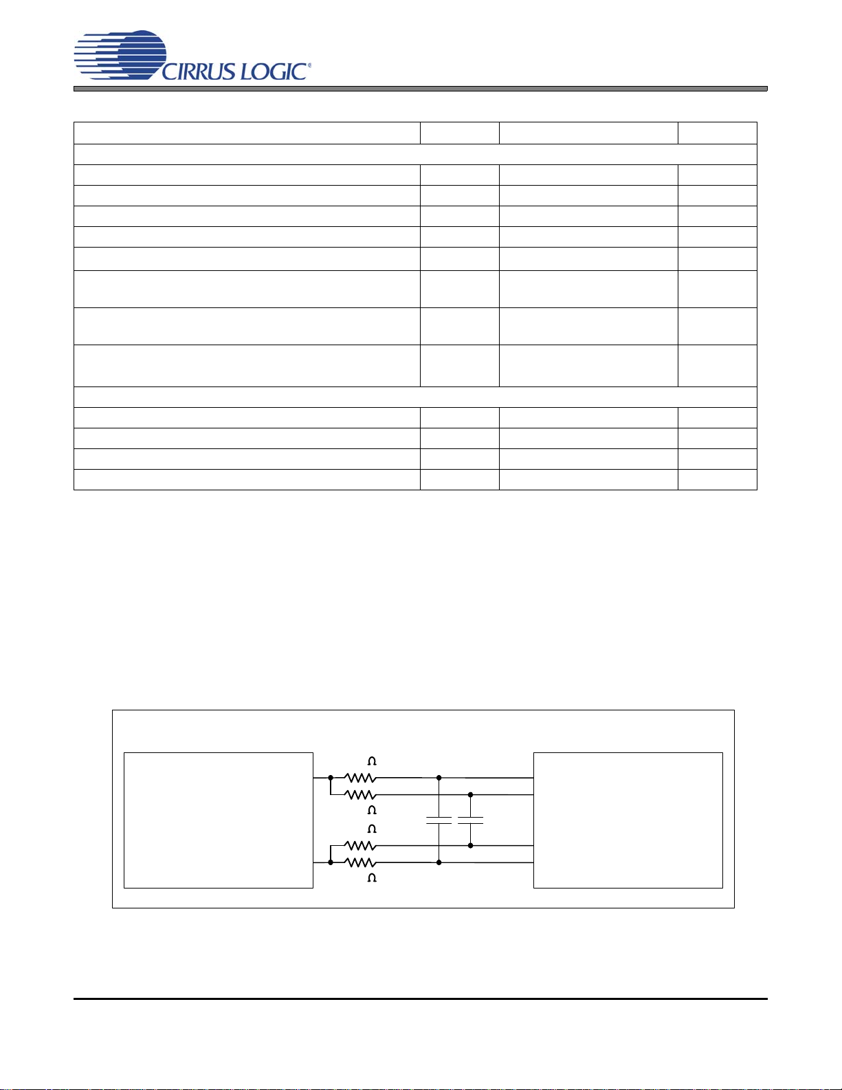
7. VOLTAGE REFERENCE
10
Ω
To VREF+
+
From VA+
Regulator
2.500 V
VREF
0.1 μF
To VREF-
0.1 μF
100 μF
0.1 μF
0.1 μF
0.1 μF
100 μF
100 μF
From VARegulator
Route VREF± as a differential pair
from the 100uF RC filter capacitor
Figure 18. Voltage Reference Circuit
CS5374
CS5374
The CS5374 modulators require a 2.500 V precision voltage reference to be supplied to the VREF±
pins.
7.1 VREF Power Supply
To guarantee proper regulation headroom for the
voltage reference device, the voltage reference
GND pin should be connected to VA– instead of
system ground, as shown in Figure 18. This connection results in a VREF– voltage equal to VA–
and a VREF+ voltage very near ground potential
[(VA–) + 2.500 VREF].
Power supply inputs to the voltage reference device
should be bypassed to system ground with 0.1 μF
capacitors placed as close as possible to the power
and ground pins. In addition to 0.1 μF local bypass
capacitors, at least 100 μF of bulk capacitance to
system ground should be placed on each power
supply near the voltage regulator outputs. Bypass
capacitors should be X7R, C0G, tantalum, or other
high-quality dielectric type.
A separate RC filter is required for each device
connected to the voltage reference output. Signaldependent sampling of the voltage reference by one
system device could cause unwanted tones to appear in the measurement bandwidth of another system device if a single VREF RC filter is common
to both.
7.3 VREF PCB Routing
To minimize the possibility of outside noise coupling into the CS5374 voltage reference input, the
VREF± traces should be routed as a differential
pair from the large capacitor of the voltage reference RC filter. Careful control of the voltage reference source and return currents by routing VREF±
as a differential pair will significantly improve immunity from external noise.
To further improve noise rejection of the VREF
differential route,
tors to system ground as close as possible to the
VREF+ and VREF– pins of the CS5374.
include 0.1 μF bypass capaci-
±
7.2 VREF RC Filter
A primary concern in selecting a precision voltage
reference device is noise performance in the measurement bandwidth. The Linear Technology
LT1019AIS8-2.5 voltage reference yields accept-
able noise levels if the output is filtered with a lowpass RC filter.
30
7.4 VREF Input Impedance
The switched-capacitor input architecture of the
VREF± inputs results in an input impedance that
depends on the internal capacitor size and the
MCLK frequency. With a 15 pF internal capacitor
and a 2.048 MHz MCLK, the VREF input impedance is approximately
Page 31

1 / [(2.048 MHz) x (15 pF)] = 32 kΩ. While the
size of the internal capacitor is fixed, the voltage
reference input impedance can vary with MCLK.
The voltage reference external RC filter series resistor creates a voltage divider with the VREF input impedance to reduce the effective applied input
voltage. To minimize gain error resulting from this
voltage divider effect, the RC filter series resistor
should be the minimum size recommended in the
voltage reference device data sheet.
7.5 VREF Accuracy
The nominal voltage reference input is specified as
2.500 V across the VREF± pins, and all CS5374
gain accuracy specifications are measured using a
nominal voltage reference input. Any variation
from a nominal VREF input will proportionally
vary the analog full-scale gain accuracy.
CS5374
CS5374
Since temperature drift of the voltage reference results in gain drift of the analog full-scale amplitude,
care should be taken to minimize temperature drift
effects through careful selection of passive components and the voltage reference device itself. Gain
drift specifications of the CS5374 do not include
the temperature drift effects of external passive
components or of the voltage reference device itself.
31
Page 32

8. POWER SUPPLIES
CS5374
VA+
VD+
VA- GND
0.01 uF 1 00 uF0.1 uF100 uF
100 uF
0.1 uF
To VA+
Regulator
To VA-
Regulator
To VD
Regulator
VA+
VA-
0.1 uF
0.1 uF
Figure 19. Power Supply Diagram
CS5374
CS5374
The CS5374 has two positive analog power supply
pins (VA+), two negative analog power supply
pins (VA–), a digital power supply pin (VD+), and
a ground pin (GND).
For proper operation, power must be supplied to all
power supply pins, and the ground pin must be connected to system ground. The CS5374 digital power supply (VD+) and the CS5376A digital power
supply (VD) must share a common voltage.
8.1 Analog Power Supplies
The analog power pins of the CS5374 are to be supplied with a total of 5 V between VA+ and VA–
from a bipolar ±2.5 V supply. When using bipolar
supplies the analog signal common mode voltage
should be biased to 0 V. The analog power supplies
are recommended to be bypassed to system ground
using 0.1 μF X7R type capacitors.
The VA– supply is connected to the CMOS substrate and as such must remain the most negative
applied voltage to prevent potential latch-up conditions. It is recommended to clamp the VA– supply
to system ground using a reverse biased Schottky
diode to prevent possible latch-up conditions related to mismatched supply rail initialization.
32
Care should be taken to connect the CS5374 thermal pad on the bottom of the package to VA–, not
system ground (GND), since it internally connects
to VA– and is expected to be the most negative applied voltage.
8.2 Digital Power Supply
The digital power supply across the VD and GND
pins is specified for a +3.3 V power supply. The
digital power supply should be bypassed to system
ground using a 0.01 μF X7R type capacitor. The
digital power supply across the VD+ and GND pins
is specified to be +3.3 V.
8.3 Power Supply Bypassing
The VA+ and VA– power supplies should be bypassed to system ground with 0.1 μF capacitors
placed as close as possible to the power pins of the
device. The VD+ power supply should be bypassed
to system ground with 0.1 μF capacitors placed as
close as possible to the power pins of the device.
Bypass capacitors should be X7R, C0G, tantalum,
or other high-quality dielectric type.
In addition to the local bypass capacitors, at least
100 μF bulk capacitance to system ground should
be placed on each power supply near the voltage
Page 33

CS5374
CS5374
regulator output, with additional power supply
bulk capacitance placed among the analog component route if space permits.
8.4 PCB Layers and Routing
The CS5374 is a high-performance device, and
special care must be taken to ensure power and
ground routing is correct. Power can be supplied either through dedicated power planes or routed traces. When routing power traces, it is recommended
to use a “star” routing scheme with the star point either at the voltage regulator output or at a local
power supply bulk capacitor.
It is also recommended to dedicate a full PCB layer
to a solid ground plane, without splits or routing.
All bypass capacitors should connect between the
power supply circuit and the solid ground plane as
near as possible to the device power supply pins.
The CS5374 analog signals are differentially routed and do not normally require connection to a separate analog ground. However, if a separate analog
ground is required, it should be routed using a
“star” routing scheme on a separate layer from the
solid ground plane and connected to the ground
plane only at a single point. Be sure all active devices and passive components connected to the
separate analog ground are included in the “star”
route to ensure sensitive analog currents do not return through the ground plane.
8.5 Power Supply Rejection
Power supply rejection of the CS5374 is frequency
dependent. The CS5376A digital filter fully rejects
power supply noise for frequencies above the selected digital filter corner frequency. Power supply
noise frequencies between DC and the digital filter
corner frequency are rejected as specified in the
“Power Supply Characteristics” on page 13.
8.6 SCR Latch-up Considerations
It is recommended to connect the VA– power supply to system ground (GND) through a reverse-biased Schottky diode. At power up, if the VA+
power supply ramps up before the VA– supply is
established, the VA- pin voltage could be pulled
above ground potential through the CS5374 device. If the VA– supply is pulled 0.7 V or more
above GND, SCR latch-up can occur. A reverse-biased Schottky diode will clamp the VA– voltage a
maximum of 0.3 V above ground to ensure SCR
latch-up does not occur at power up.
For similar reasons, care should be taken to connect
the CS5374 thermal pad on the bottom of the package to VA–, not system ground (GND), since it internally connects to VA– and is expected to be the
most negative applied voltage.
8.7 DC-DC Converters
Many low-frequency measurement systems are
battery powered and utilize DC-DC converters to
efficiently generate power supply voltages. To
minimize interference effects, operate the DC-DC
converter at a frequency which is rejected by the
digital filter, or operate it synchronous to the
MCLK rate.
A synchronous DC-DC converter whose operating
frequency is derived from MCLK will theoretically
minimize the potential for “beat frequencies” to appear in the measurement bandwidth. However this
requires the source clock to remain jitter free within the DC-DC converter circuitry. If clock jitter can
occur within the DC-DC converter (as in a PLLbased architecture), it’s better to use a non-synchronous DC-DC converter whose switching frequency is rejected by the digital filter.
During PCB layout, do not place high-current DCDC converters near sensitive analog components.
Carefully routing a separate DC-DC “star” ground
will help isolate noisy switching currents away
from the sensitive analog components.
33
Page 34

9. SPITM REGISTER SUMMARY
The CS5374 Configuration Registers contain
the hardware configuration settings.
Name Addr. Type # Bits Description
VERSION
AMP1CFG
AMP2CFG
ADCCFG
PWRCFG
0x00 R 8
0x01 R/W 8
0x02 R/W 8
0x03 R/W 8
0x04 R/W 8
CS5374
CS5374
Device Version ID
Amplifier 1 configuration
Amplifier 2 configuration
Modulator 1 & 2 configuration
Power configuration
34
Page 35

9.1 VERSION: 0x00
(MSB)7654321(LSB)0
VER7 VER6 VER5 VER4 VER3 VER2 VER1 VER0
RRRRRRRR
01000001
Figure 20. Hardware Version ID Register VERSION
Bit definitions:
7:0 VERS Hardware revision ID register
0x41: Revision A
Address: 0x00
-- Not defined
(read as 0)
R Readable
WWritable
R/W Readable
and Writable
Bits in bottom rows
are reset condition
Reset Condition : 0100_0001 (0x41) : Default value
Normal Operation : 0100_0001 (0x41) : Default value
Power Down Operation : 0100_0001 (0x41) : Default value
CS5374
CS5374
35
Page 36

CS5374
(MSB)7654321(LSB)0
PWDN1 HP1 MUX1_1 MUX1_0 GUARD GAIN1_2 GAIN1_1 GAIN1_0
R/W R/W R/W R/W R/W R/W R/W R/W
00000000
Figure 21. Amplifier 1 Configuration Register AMP1CFG
Bit definitions:
7 PWDN1 Amplifier 1 Power Down
1: enable
0: disable
6 HP1 Amplifier 1 High Precision
1: enable
0: disable
5:4 MUX1[1:0] Input Multiplexer
11: INA1 + INB1
10: INA1 only
01: INB1 only
00: 800 ohm termination
3 GUARD GUARD Output
1: disable
0: enable
2:0 GAIN1[2:0] Amplifier 1 Gain
111: reserved
110: 64x
101: 32x
100: 16x
011: 8x
010: 4x
001: 2x
000: 1x
Address: 0x01
-- Not defined
(read as 0)
R Readable
WWritable
R/W Readable
and Writable
Bits in bottom rows
are reset condition
Reset Condition : 0000_0000 (0x00) : Default value
Normal Operation : 00MM_GGGG : MUX, GUARD and GAIN select
Power Down Operation : 1000_0000 (0x80) : PWDN enabled
9.2 AMP1CFG: 0x01
CS5374
36
Page 37

CS5374
(MSB)7654321(LSB)0
PWDN2 HP2 MUX2_1 MUX2_0 --- GAIN2_2 GAIN2_1 GAIN2_0
R/W R/W R/W R/W R/W R/W R/W R/W
00000000
Figure 22. Amplifier 2 Configuration Register AMP2CFG
Bit definitions:
7 PWDN2 Amplifier 2 Power Down
1: enable
0: disable
6 HP2 Amplifier 2 High Precision
1: enable
0: disable
5:4 MUX2[1:0] Input Multiplexer
11: INA2 + INB2
10: INA2 only
01: INB2 only
00: 800 ohm termination
3--- Reserved
2:0 GAIN2[2:0] Amplifier 2 Gain
111: reserved
110: 64x
101: 32x
100: 16x
011: 8x
010: 4x
001: 2x
000: 1x
Address: 0x02
-- Not defined
(read as 0)
R Readable
WWritable
R/W Readable
and Writable
Bits in bottom rows
are reset condition
Reset Condition : 0000_0000 (0x00) : Default value
Normal Operation : 00MM_0GGG : MUX and GAIN select
Power Down Operation : 1000_0000 (0x80) : PWDN enabled
9.3 AMP2CFG: 0x02
CS5374
37
Page 38

CS5374
(MSB)7654321(LSB)0
OFST
HP PWDN2 PWDN1 --- --- --- ---
R/W R/W R/W R/W R/W R/W R/W R/W
00000000
Figure 23. Modulator 1 & 2 Configuration Register ADCCFG
Bit definitions:
7OFSTModulator Offset
(add -60mV to Channel 1,
add -35mV to Channel 2)
1: disable
0: enable
6 HP Modulator High Precision
1: enable
0: disable
5 PWDN2 Modulator 2 Power Down
1: enable
0: disable
4 PWDN1 Modulator 1 Power Down
1: enable
0: disable
3:0 --- Reserved
Address: 0x03
-- Not defined
(read as 0)
R Readable
WWritable
R/W Readable
and Writable
Bits in bottom rows
are reset condition
Reset Condition : 0000_0000 (0x00) : Default value
Normal Operation : 0100_0000 (0x40) : HP mode enabled
Power Down Operation : 0011_0000 (0x30) : PWDN enabled
9.4 ADCCFG: 0x03
CS5374
38
9.5 PWRCFG: 0x04
Page 39

CS5374
(MSB)7654321(LSB)0
adc_lpwr --- amp_i1_1 amp_i1_0 rough i1_tail amp_i5_1 amp_i5_0
R/W R/W R/W R/W R/W R/W R/W R/W
00000000
Figure 24. Power Configuration Register PWRCFG
Bit definitions:
7 adc_lpwr Modulator Bias
1: reduced current
0: nominal current
6 --- reserved
5:4 amp_i1 Amplifier i1 Bias
11: 2/3
10: 1/3
01: 4/3
00: nominal current
3 rough Modulator Rough Phase
1: reduced current
0: nominal current
2 i1_tail Amplifier i1 Tail Current
1: reduced current
0: nominal current
1:0 amp_i5 Amplifier i5 Bias
11: 7/11
10: 9/13
01: 15/13
00: nominal current
Address: 0x04
--- Not defined
(read as 0)
R Readable
WWritable
R/W Readable
and Writable
Bits in bottom rows
are reset condition.
Reset Condition : 0000_0000 (0x00) : Default value
Normal Operation : 1000_1111 (0x8F) : Reduced power
Power Down Operation : 0000_0000 (0x00) : Default value
CS5374
39
Page 40

10. PIN DESCRIPTIONS
INA2-
INA2+
11
12
Top-Down
(Though Package)
View
Pin 1 Location
Indicators
INA1+
INA1INB1-
INB1+
DNC
VA+
VA-
DNC
INB2+
INB2-
1
2
3
4
5
6
7
MCLK
MSYNC
MDATA1
MFLAG1
36
35
34
33
VD+
GND
MDATA2
32
31
30
GUARD2
OUT2+
OUT2-
INR2-
INF2-
INF2+
INR2+
19
18
17
16
15
14
13
GUARD1
OUT1+
OUT1-
INR1-
INF1-
INF1+
INR1+
48
47
46
45
44
43
42
8
9
10
NC
VREF+
VREF-
22
21
20
NC
NC
24
23
MFLAG2
SDO
SDI
29
28
27
SCLK
CS
26
25
NC
VA-
VA+
41
40
39
NC
RST
38
37
THERMAL
PAD
CONNECT
TO VA-
CS5374
CS5374
40
Pin
Name
VA+
VA–
VD+,
GND
INA1+
INA1–
INB1–,
INB1+
INB2+,
INB2–
INA2–,
INA2+
Pin
Number
6, 39
7, 40
32,
31
1
2
3
4
9
10
11
12
Pin
Type
I
I
Differential Amplifier Analog Inputs
I
I
I
I
Power Supplies
Analog power supply.
Refer to the Specified Operating Conditions.
Digital power supply.
Refer to the Specified Operating Conditions.
Channel 1 differential analog input A.
Selected via Serial Communications Interface.
Channel 1 differential analog input B.
Selected via Serial Communications Interface.
Channel 2 differential analog input B.
Selected via Serial Communications Interface.
Channel 2 differential analog input A.
Selected via Serial Communications Interface.
Pin
Description
Page 41

Differential Amplifier Analog Outputs
OUT1–,
OUT1+
46
47
GUARD1 48 O
GUARD2 13 O
OUT2+,
OUT2–
14
15
Modulator Analog Inputs
INR1+,
INF1+,
INF1–,
INR1–
INR2–,
INF2–,
INF2+,
INR2+
VREF+,
VREF–
42
43
44
45
16
17
18
19
21
22
CS 25 I
SCLK 26 I
SDI 27 I
SDO 28 O
MCLK 36 I
MSYNC 35 I
MFLAG1 33 O
MDATA1 34 O
MFLAG2 29 O
MDATA2 30 O
CS5374
O
O
I
I
I
Modulator Interface
Channel 1 differential analog output.
Guard output voltage for analog input Channel 1.
Guard output voltage for analog input Channel 2.
Channel 2 differential analog output.
Channel 1 analog differential rough and fine inputs.
From the Channel 1 differential anti-alias filter.
Channel 2 analog differential rough and fine inputs.
From the Channel 2 differential anti-alias filter.
Volta g e Re f er e n c e
Voltage reference input.
Refer to the Specified Operating Conditions.
Serial Interface
Chip select. Active low.
Serial clock.
Serial data in to device.
Serial data out of device.
Modulator clock input.
Modulator sync input.
Channel 1 modulator flag output.
Channel 1 modulator data output.
Channel 2 modulator flag output.
Channel 2 modulator data output.
CS5374
RST 37 I
NC 20, 23, 24,
38, 41
DNC 5, 8 ---
Thermal Pad 49 I
---
Device Reset
Reset. Active low.
Other
No connect.
Do Not Connect.
Connect to VA–. Do not connect to GND.
41
Page 42

11. PACKAGE DIMENSIONS
48-PIN QFN (7MM X 7MM)
CS5374
CS5374
42
Page 43

CS5374
CS5374
12. ORDERING INFORMATION
Model Number Temperature Package
CS5374-CNZ, lead (Pb) free -10 to +70 °C 48-Pin QFN
13. ENVIRONMENTAL, MANUFACTURING, & HANDLING INFORMATION
Model Number Peak Reflow Temp MSL Rating* Max Floor Life
CS5374-CNZ, lead (Pb) free 260 °C 3 7 Days
* MSL (Moisture Sensitivity Level) as specified by
IPC/JEDEC J-STD-020.
43
Page 44

CS5374
Contacting Cirrus Logic Support
For all product questions and inquiries contact a Cirrus Logic Sales Representative.
To find one nearest you go to www.cirrus.com
IMPORTANT NOTI CE
"Preliminary" product information describes products that are in production, but for which full characterization data is not yet available.
Cirrus Logic, Inc. and its subsidiaries (“Cirrus”) believe that the information contained i n thi s doc ument is ac cur ate an d rel i able. However, the information is subject
to change without not ice and is prov ided “AS IS” wit hout warra nty of any ki nd (express or implied) . Customers are advised to obt ain the lat est vers ion of relev ant
information to verify, before placing orders, that information being relied on is current and complete. All products are sold subject to the terms and conditions of sale
supplied at the time of order acknowledgment, including those pertaining to warranty, indemnification, and limitation of liability. No responsibility is assu med by Cirrus
for the use of this information, inclu ding u se of this in form ation as the basis for ma nufactur e or sale of a ny item s, or for in fringement of patents or other rights of third
parties. This document is the property of Cir ru s and by furnishing this information, Cirrus grants no license, express or implied under any patents, mask work rights,
copyrights, trademarks, trade secrets or other intellectual property rights. Cirrus owns the copyrights associated with the information contained herein and gives consent for copies to be made of t he information only for use within your organization with respect to Cirrus integrated circuit s or other products of Cirrus. This consent
does not extend to other copying such as copying for gen e ral distribu tion , advertising or promotional purposes, or for creating an y work for re sale.
CERTAIN APPLICATIONS USING SEMICONDUCTOR PRODUCTS MAY INVOLVE POTENTIAL RISKS OF DEATH, PERSONAL INJURY, OR SEVERE PROPERTY OR ENVIRONMENTAL DAM AGE (“CRITICAL APPLICATIONS”). CIRRUS PRODUCTS ARE NOT DESIGNED, AUTHORIZED OR WARRANTED FOR USE
IN PRODUCTS SURGICALLY IMPLANTED INTO THE BODY, A UTOMOTIVE SA FETY, S ECURITY DEVI CES, L IFE SUP PORT PRODUCTS OR OTHE R CRITICAL APPLICATIONS. INCLUSION OF CIRRUS PRODUCTS IN SUCH APPLICATIONS IS UNDERSTOOD T O BE FULLY AT THE C USTOM ER'S R ISK AND CIRRUS DISCLAIMS AND MAKES NO WARRANTY, EXPRESS, STATUTORY OR IMPLIED, INCLUDING THE IMPLIED WARRANTIES OF MERCHANTABILITY AND
FITNESS FOR PARTICULAR PURPOSE, WITH REGARD TO ANY CIRRUS PRODUCT THAT IS USED IN SUCH A MANNER. IF THE CUSTOM ER OR CUSTOMER'S CUSTOMER USES OR PERMITS THE USE OF CIRRUS PRODUCTS IN CRITICAL APPLICATIONS, CUSTOMER AGREES, BY SUCH USE, TO FULLY
INDEMNIFY CIRRUS, ITS OFF ICER S, DI RECTOR S, EMPL OYEES, DISTR IBUTO RS AND OTHER AGENTS FROM ANY AND ALL LIABILI TY, I NCLUDING AT TORNEYS' FEES AND COSTS, THAT MAY RESULT FROM OR ARISE IN CONNECTION WITH THESE USES.
Cirrus Logic, Cirrus, and the Cirrus Logic logo designs are trademarks of Cirrus Logic, Inc. All other brand and product names in this document may be trademarks
or service marks of their respective owners.
SPI is a trademark of Motorola, Inc.
14. REVISION HISTORY
Revision Date Changes
T1 AUG 2008 Initial release of Target data sheet.
A1 DEC 2008 Initial release of Advanced data sheet.
A2 JAN 2009 Update to include more complete characterization data.
PP1 APR 2009 Specify operation for 2.048 MHz MCLK and HP mode. Add PWRCFG register.
Update to include more complete characterization data.
F1 OCT 2009 Update to include final characterization data.
F2 SEP 2010 Corrected VERSION register default value to 0100 0001 (0x41) — CS5374, Rev A.
CS5374
44
 Loading...