

Page 1
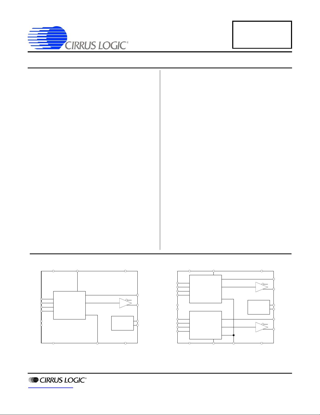
CS5371A
Clock
Generator
INF1+
VREF+
VREF-
VA+
VA-
VD
GND
PWDN1
MFLAG1
MDATA1
MCLK
MSYNC
MFLAG2
MDATA2
PWDN2
INF1INR1-
INR1+
INF2+
INF2INR2-
INR2+
4th Order
ΔΣ Modulator
4th Order
ΔΣ Modulator
OFST
CS5372A
Clock
Generator
INF+
VREF+
VREF-
VA+
VA-
VD
GND
PWDN
MFLAG
MDATA
MCLK
MSYNC
INFINR-
INR+
4th Order
ΔΣ Modulator
OFST
CS5371A
CS5372A
Low-power, High-performance
Features
Fourth-order ΔΣ Architecture
Clock-jitter-tolerant Architecture
Input Voltage: 5 V
Input Signal Bandwidth: DC to 2 kHz
High Dynamic Range
• 127 dB SNR @ 215 Hz BW (2 ms sampling)
• 124 dB SNR @ 430 Hz BW (1 ms sampling)
Low Total Harmonic Distortion
• -118 dB THD typical (0.000126%)
Low Power Consumption
• Normal operation: 25 mW per channel
• Power down: 10 µW per channel
Small Footprint, 24-pin SSOP package
Multi-channel System Support
• 1-channel System: CS5371A
• 2-channel System: CS5372A
• 3-channel System: CS5371A + CS5372A
• 4-channel System: CS5372A + CS5372A
Bipolar Power Supply Configuration
• VA+ = +2.5 V; VA- = -2.5 V; VD = +3.3 V
Fully Differential
pp
ΔΣ
Modulators
Description
The CS5371A and CS5372A are one- and two-channel,
high-dynamic-range, fourth-order ΔΣ modulators intended for geophysical and sonar applications. When
combined with CS3301A / CS3302A differential amplifiers, the CS4373A test DAC and CS5376A digital filter, a
small, low-power, self-testing, high-accuracy, multichannel measurement system results.
The modulators have high dynamic range and low total
harmonic distortion with very low power consumption.
They convert differential analog input signals from the
CS3301A / CS3302A amplifiers to an oversampled serial bit stream at 512 kbits per second. This oversampled
bit stream is then decimated by the CS5376A digital filter
to a 24-bit output at the selected output word rate.
In normal operation, power consumption is 5 mA per
channel. Each modulator can be independently powered
down to 500 µA per channel, and by halting the input
clock they will enter a micro-power state using only 2 µA
per channel.
The CS5371A and CS5372A modulators are available in
small 24-pin SSOP packages, providing exceptional performance in a very small footprint.
ORDERING INFORMATION
See page 30.
http://www.cirrus.com
Copyright Cirrus Logic, Inc. 2010
(All Rights Reserved)
SEP ‘10
DS748F3
Page 2

TABLE OF CONTENTS
1. CHARACTERISTICS AND SPECIFICATIONS ........................................................................ 4
SPECIFIED OPERATING CONDITIONS.................................................................................4
ABSOLUTE MAXIMUM RATINGS ........................................................................................... 4
TEMPERATURE CONDITIONS ...............................................................................................5
ANALOG INPUT CHARACTERISTICS ................................................................................... 5
PERFORMANCE CHARACTERISTICS..................................... ......................................... .... . 6
PERFORMANCE CHARACTERISTICS (CONT.) .................. .... ... ... ... ... .... ... ... ... .... ... ... ... ... .... . 7
PERFORMANCE PLOTS.................... ... ... .......................................... ... .... ... ........................... 8
DIGITAL CHARACTERISTICS ................................................................................................9
DIGITAL CHARACTERISTICS (CONT.) ...............................................................................10
DIGITAL CHARACTERISTICS (CONT.) ............................................................................11
POWER SUPPLY CHARACTERISTICS................................................................................ 12
2. SYSTEM DIAGRAM ............................................................................................................13
3. MODULATOR OPERATION ................................................................................................... 14
3.1 One’s Density ...................................... ... .... ... ... ... .......................................... ...................14
3.2 Decimated 24-bit Output ..................................................................................................15
3.3 Synchronization .................................. ... .... ... .......................................... .........................15
3.4 Idle Tones ........................ ... ... .... ...................................... .... ... ... ... ... .... ... .........................15
3.5 Stability ...................................... ... ... ....................................... ... ... ... .... ... ... ... ...................15
4. ANALOG SIGNALS ................................................................................................................ 16
4.1 INR±, INF± Modulator Inputs ........... ... ... .......................................................................... 16
4.2 Input Impedance ........................ ... ... ... ... .... ... ... ... .......................................... ...................16
4.3 Anti-alias Filter .................... ....................................... ... ... .... ... ... ... ... ................................ 17
4.4 Analog Differential Signals ......... ... ... ... ... .... .......................................... ... ... ... .... ... ... ... ... ... 17
5. DIGITAL SIGNALS .................................................................................................................18
5.1 MCLK Connection .. ... .... ... ... ... .... ... ....................................... ... ... ... ... .... ... ... ......................18
5.2 MSYNC Connection ................................... ... ... ... ....................................... ... .... ... ... ... ... ... 18
5.3 MDATA Connection ......................... ... ... .... ... ... ... .......................................... .... ... ... .........19
5.4 MFLAG Connection ...................................... ... ... .... ... ... ...................................................19
5.5 OFST Connection ...................... ... ... ... .......................................... ...................................19
6. POWER MODES ..................................................................................................................... 20
6.1 Normal Operation ................................... .... ... ... ... .... .........................................................20
6.2 Power Down, MCLK Enabled .......................................................................................... 20
6.3 Power Down, MCLK Disabled .................................... ... ... .... ... ... ... ... .... ... ... ... .... ... ... ... ......20
7. VOLTAGE REFERENCE ........................................................................................................21
7.1 VREF Power Supply ........................... ... .... ... ... ... .... .........................................................21
7.2 VREF RC Filter ................................................................................................................21
7.3 VREF PCB Routing ..........................................................................................................21
7.4 VREF Input Impedance ....................................................................................................21
7.5 VREF Accuracy ................................... ... .... ... ... ................................................................22
8. POWER SUPPLIES ................................................................................................................23
8.1 Power Supply Bypassing .................... ... .... ... ... ... .... ... .......................................... ... ... ... ... 23
8.2 PCB Layers and Routing ........................................... ... ... .... ... ... ... ... .... ... ... ... ...................23
8.3 Power Supply Rejection ... ... ... .... .......................................... ... ... ...................................... 23
8.4 SCR Latch-up Considerations ......................................................................................... 24
8.5 DC-DC Converters . ... .... ... ... .............................................................................................24
9. PIN DESCRIPTION - CS5371A ............................................................................................. 25
10. PIN DESCRIPTION - CS5372A ........................................................................................... 27
11. PACKAGE DIMENSIONS ..................................................................................................... 29
12. ORDERING INFORMATION ................................................................................................ 30
13. ENVIRONMENTAL, MANUFACTURING, & HANDLING INFORMATION ....... ................... 31
14. REVISION HISTORY ........................................................................................................... 32
CS5371A CS5372A
2 DS748F3
Page 3

LIST OF FIGURES
Figure 1. Anti-alias Filter Components............................................................................................ 5
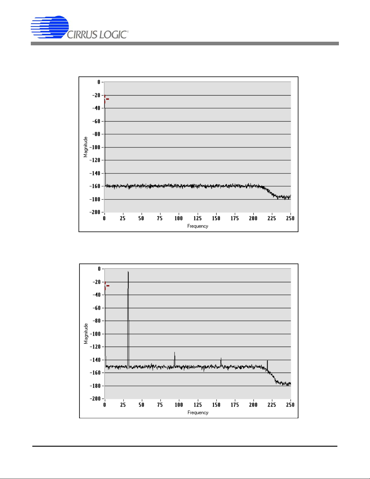
Figure 2. Modulator Noise Performance......................................................................................... 8
Figure 3. Modulator + CS4373A Test DAC Dynamic Performance ............................... ... ... ... ... .... . 8
Figure 4. Digital Input Rise and Fall Times .....................................................................................9
Figure 5. Digital Output Rise and Fall Times .................................................................................. 9
Figure 6. System Timing Diagram.................................................................................................11
Figure 7. MCLK / MSYNC Timing Detail....................................................................................... 11
Figure 9. Connection Diagram...................................................................................................... 13
Figure 8. System Block Diagram................................................................................................... 13
Figure 10. CS5371A and CS5372A Block Diagrams.................................................................... 14
Figure 11. Analog Signals............................................................................................................. 16
Figure 12. Digital Signals.............................................................................................................. 18
Figure 13. Power Mode Diagram.................................................................................................. 20
Figure 14. Voltage Reference Circuit............................................................................................21
Figure 15. Power Supply Diagram................................................................................................ 23
LIST OF TABLES
Table 1. 24-Bit Output Coding for the CS5371A and CS5372A Modulator and
CS5376A Digital Filter Combination ............................................................................. 15
CS5371A CS5372A
DS748F3 3
Page 4
CS5371A CS5372A
1. CHARACTERISTICS AND SPECIFICATIONS
• Min / Max characteristics and specifications are guaranteed over the Specified Operating Conditions.
• Typical performance characteristics and specifications are measured at nominal supply voltages and T
• GND = 0 V. Single-ended voltages with respect to GND, differential voltages with respect to opposite half.
• Device is connected as shown in Figure 9 on page 13 unless otherwise noted.
SPECIFIED OPERATING CONDITIONS
Parameter Symbol Min Nom Max Unit
Bipolar Power Supplies
Positive Analog ± 2% VA+ 2.45 2.50 2.55 V
Negative Analog (Note 1) ± 2% VA- -2.45 -2.50 -2.55 V
Positive Digital ± 3% VD 3.20 3.30 3.40 V
Voltage Reference
[VREF+] - [VREF-] (Note 2, 3) VREF - 2.500 - V
VREF- (Note 4)VREF- - VA- - V
Thermal
Ambient Operating Temperature Industrial (-ISZ) T
A
-40 25 85 °C
= 25°C.
A
Notes: 1. VA- must always be the most-negative input voltage to avoid potential SCR latch-up conditions.
2. By design, a 2.500 V voltage reference input results in the best signal-to-noise performance.
3. Channel-to-channel gain accuracy is directly proportional to the voltage reference absolute accuracy.
4. VREF inputs must satisfy: VA- ≤ VREF- < VREF+ ≤ VA+.
ABSOLUTE MAXIMUM RATINGS
Parameter Symbol Min Max Parameter
DC Power Supplies Positive Analog
Negative Analog
Digital
Analog Supply Differential (VA+) - (VA-) VA
Digital Supply Differential (VD) - (VA-) VD
Input Current, Power Supplies (Note 5)I
Input Current, Any Pin Except Supplies (Note 5, 6)I
Output Current (Note 5)I
VA+
VA-
VD
DIFF
DIFF
PWR
IN
OUT
-0.5
-6.8
-0.5
-6.8V
-6.8V
-±50mA
-±10mA
-±25mA
6.8
0.5
6.8
Power Dissipation PDN - 500 mW
Analog Input Voltages V
Digital Input Voltages V
Storage Temperature Range T
INA
IND
STG
(VA-) - 0.5 (VA+) + 0.5 V
-0.5 (VD) + 0.5 V
-65 150 ºC
V
V
V
WARNING: Operation at or beyond these limits may result in permanent damage to the device.
Normal operation is not guaranteed at these extremes.
Notes: 5. Transient currents up to ±100 mA will not cause SCR latch-up.
6. Includes continuous over-voltage conditions at the modulator analog input pins.
4 DS748F3
Page 5
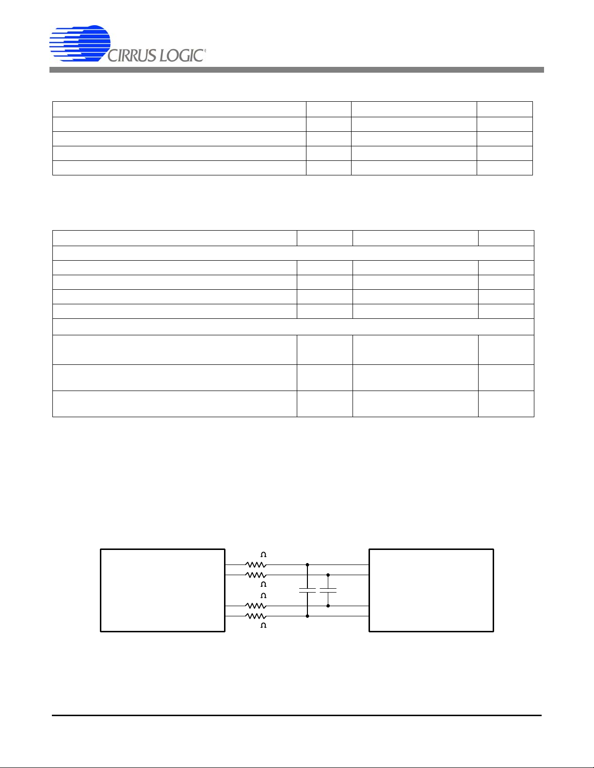
TEMPERATURE CONDITIONS
CS5371A / CS5372A
MODULATOR
INR+
INF+
INFINR-
20nF
C0G
20nF
C0G
680
CS3301A / CS3302A
AMPLIFIER
OUTR+
OUTF+
OUTFOUTR-
680
680
680
Figure 1. Anti-alias Filter Components
Parameter Symbol Min Typ Max Unit
Ambient Operating Temperature T
Storage Temperature Range T
Allowable Junction Temperature T
Junction to Ambient Thermal Impedance (4-layer PCB) θ
A
STR
JCT
JA
CS5371A CS5372A
-40 - 85 ºC
-65 - 150 ºC
--125ºC
-65-ºC/W
ANALOG INPUT CHARACTERISTICS
Parameter Symbol Min Typ Max Unit
VREF Input
[VREF+] - [VREF-] (Note 2, 3) VREF - 2.500 - V
VREF- (Note 4)VREF- - VA- - V
VREF Input Current VREF
VREF Input Noise (Note 7)VREF
IMOD
IN
-120- µA
--1µV
rms
Modulator INR±, INF± Inputs
External Anti-alias Filter Series Resistance
(Note 8) Differential Capacitance
Differential Input Impedance INR±
INF±
Single-ended Input Impedance INR±
INF±
R
C
DIFF
ZDIF
ZDIF
ZSE
ZSE
AA
INR
INF
INR
INF
-
-
-
-
-
-
680
20
20
1
40
2
-
-
-
-
-
-
Ω
nF
kΩ
MΩ
kΩ
MΩ
Notes: 7. Maximum integrated noise over the measurement bandwidth for the voltage reference device attached
to the VREF± inputs.
8. Anti-alias capacitors are discrete external components and must be of good qu ality (C0G, NPO, poly).
Poor quality capacitors will degrade total harmonic distortion (THD) performance. See Figure 1 on
page 5
DS748F3 5
Page 6
CS5371A CS5372A
PERFORMANCE CHARACTERISTICS
Parameter Symbol Min Typ Max Unit
Signal Characteristics
Input Signal Frequencies (Note 9, 10) V
Full-scale Differential AC Input (Note 9)V
Full-scale Differential DC Input (Note 9)V
Input Common Mode Voltage (Note 11) V
Input Voltage Range (V
±Signal) (Note 9) V
cm
BW
AC
DC
CM
RNG
Dynamic Performance
Dynamic Range (1/4 ms) DC to 1720 Hz
SNR -
(Note 10, 12) (1/2 ms) DC to 860 Hz
(1 ms) DC to 430 Hz
(2 ms) DC to 215 Hz
(4 ms) DC to 108 Hz
(8 ms) DC to 54 Hz
(16 ms) DC to 27 Hz
Signal-dependent Noise (1 ms) DC to 430 Hz
SDN 100 110 - dB
(Note 13, 14)
Total Harmonic Distortion (Note 14) THD - -118 -112 dB
Linearity (Note 14)LIN Total Harmonic Distortion (Note 15)THD - -110 - dB
Linearity (Note 15)LIN Common Mode Rejection Ratio CMRR - 110 - dB
Channel Crosstalk (CS5372A only) CXT - -150 - dB
DC - 2000 Hz
--5V
pp
-2.5 - 2.5 V
- (VA-)+2.5 -V
(VA-)+0.7
-
121
-
-
-
-
- (VA+)-1.25 V
109
121
124
127
130
133
136
0.000126 0.000251
0.000316
-
-
-
-
-
-
-
-%
dB
dB
dB
dB
dB
dB
dB
%
Notes: 9. Guaranteed by design and/or characterization.
10. The upper bandwidth limit is determined by the digital filter cut-off frequency.
11. Common mode voltage is defined as the mid-point of the differential signal.
12. Dynamic Range defined as 20 log [ (RMS full scale) / (RMS idle noise) ] where idle noise is measured
from a CS3301A / CS3302A amplifier terminated input at 1x gain.
13. Signal-dependent Noise defined as 20 log [ (RMS full scale) / (RMS signal noise) ] where signal noise
is measured by subtracting out the signal power at the fundamental and harmonic frequencies.
14. Tested with a 31.25 Hz sine wave at -1 dB amplitude and Vcm = (VA-) + 2.50V.
15. Characterized with a 31.25 Hz sine wave at -1 dB amplitude and Vcm = (VA-) + 2.35V. This
corresponds to the output Vcm of the CS4373A test DAC.
6 DS748F3
Page 7
CS5371A CS5372A
PERFORMANCE CHARACTERISTICS (CONT.)
Parameter Symbol Min Typ Max Unit
Gain Accuracy
Channel to Channel Gain Accuracy (Note 3) GA - ±1 ±2 %
Channel Gain Drift (Note 16)GA
Offset
Offset Voltage, Differential (OFST = 0) OFST - ±1 - mV
Offset Voltage, CS5371A (OFST = 1) OFST - -60 - mV
Offset Voltage, CS5372A channel 1 (OFST = 1) OFST - -60 - mV
Offset Voltage, CS5372A channel 2 (OFST = 1) OFST - -35 - mV
Offset after Calibration (Note 17)OFST
Offset Calibration Range (Note 18)OFST
Offset Voltage Drift (Note 16)OFST
Notes: 16. Specification is for the parameter over the sp ecified temperature range and is for the device only. It does
not include the effects of external comp o nents.
17. Specification applies to the effective off set voltag e calculated from the output codes of the digital filter
following offset calibration and correction.
18. Offset calibration is performed in the digital filter and includes the full-scale signal range.
TC
CAL
RNG
TC
- 22 - ppm/°C
-±1- μV
-100- %FS
-300- nV/°C
DS748F3 7
Page 8
PERFORMANCE PLOTS
Figure 2. Modulator Noise Performance
Figure 3. Modulator + CS4373A Test DAC Dynamic Performance
CS5371A CS5372A
8 DS748F3
Page 9

DIGITAL CHARACTERISTICS
0.9 * VD
0.1 * VD
t
fall
t
rise
Figure 4. Digital Input Rise and Fall Times
0.9 * VD
0.1 * VD
t
fall
t
rise
Figure 5. Digital Output Rise and Fall Times
Parameter Symbol Min Typ Max Unit
Digital Inputs
High-level Input Voltage (Note 9, 19)V
Low-level Input Voltage (Note 9, 19)V
Input Leakage Current I
Digital Input Capacitance (N ot e 9) C
Input Rise Times Except MCLK (Note 9) t
Input Fall Times Except MCLK (Note 9) t
Digital Outputs
High-level Output Voltage, I
Low-level Output Voltage, I
=-40μA(Note 9)VOHVD - 0.3 - - V
out
=40μA(Note 9)V
out
High-Z Leakage Current I
Digital Output Capacitance (Note 9) C
Output Rise Times (Note 9) t
Output Fall Times (Note 9) t
IH
IL
IN
IN
RISE
FALL
OL
OZ
OUT
RISE
FALL
CS5371A CS5372A
0.6*VD - VD V
0.0 - 0.8 V
-±1±10μA
-9- pF
--100ns
--100ns
--0.3V
--±10μA
-9- pF
--100ns
--100ns
Notes: 19. Device is intended to be driven with CMOS logic levels.
DS748F3 9
Page 10
DIGITAL CHARACTERISTICS (CONT.)
Parameter Symbol Min Typ Max Unit
Master Clock Input
MCLK Frequency (Note 20)f
MCLK Period (Note 20)t
MCLK Duty Cycle (Note 9)MCLK
MCLK Rise Time (Note 9)t
MCLK Fall Time (Note 9)t
MCLK Jitter (in-band or aliased in-band) (Note 9)MCLK
MCLK Jitter (out-of-band) (Note 9)MCLK
Master Sync Input
MSYNC Setup Time to MCLK Falling (Note 9, 21)t
MSYNC Period (Note 9, 21)t
MSYNC Hold Time after MCLK Falling (Note 9, 21)t
MDATA Output
MDATA Output Bit Rate f
MDATA Output Bit Period t
MDATA Output One’s Density Range (Note 9)MDAT
Full-scale Output Code (Note 22)MDAT
CLK
mclk
RISE
FALL
OBJ
mss
msync
msh
mdata
mdata
OD
DC
IBJ
FS
CS5371A CS5372A
-2.048- MHz
-488- ns
40 - 60 %
--50ns
--50ns
--300ps
--1ns
20 122 - ns
40 976 - ns
20 122 - ns
- 512 - kbits/s
- 1953 - ns
14 - 86 %
0xA2EBE0
-
0x5D1420
Notes: 20. MCLK is generated by the digital filter. If MCLK is disabled, the device automatically enters a power-
down state.
21. MSYNC is generated by the digital filter and is latched on MCLK falling edge, synchronization instant
) is on the next MCLK rising edge.
(t
0
22. Decimated, filtered, and offset-corrected 24-bit output word from the digital filter.
10 DS748F3
Page 11

DIGITAL CHARACTERISTICS (CONT.)
MCLK
MSYNC
t
MDATA
TDATA
0
(2.048 MHz)
(512 kHz)
(256 kHz)
SYNC
MFLAG
Figure 6. System Timing Diagram
MCLK
MSYNC
t
0
(2.048 MHz)
t
mss
t
mclk
t
msync
t
msh
MDATA
(512 k Hz)
MFLAG
t
mdata
Figure 7. MCLK / MSYNC Timing Detail
CS5371A CS5372A
DS748F3 11
Page 12

CS5371A CS5372A
POWER SUPPLY CHARACTERISTICS
Parameter Symbol Min Typ Max Unit
Power Supply Current, CS5371A
Analog Power Supply Current (Note 23)I
Digital Power Supply Current (Note 23)I
A
D
Power Supply Current, CS5372A ch1 + ch2
Analog Power Supply Current (Note 23)I
Digital Power Supply Current (Note 23)I
A
D
Power Supply Current, CS5372A ch1 or ch2 only
Analog Power Supply Current (Note 23)I
Digital Power Supply Current (Note 23)I
A
D
Power Down Current, MCLK enabled
Analog Power Supply Current (Note 23)I
Digital Power Supply Current (Note 23)I
A
D
Power Down Current, MCLK disabled
Analog Power Supply Current (Note 23)I
Digital Power Supply Current (Note 23)I
Power Down Timing (after MCLK disabled) (Note 9)PD
A
D
TC
Power Supply Rejection
Power Supply Rejection Ratio (Note 24) PSRR - 100 - dB
-56mA
-75125μA
-911mA
-75125μA
-56mA
-75125μA
-0.5- mA
-75- μA
-1- μA
-1- μA
-40- μS
Notes: 23. All outputs unloaded. Digital inputs forced to VD or GND respectively.
24. Power supply rejection is characterized by applying a 100 mVp-p 50 Hz sine wave to each supply.
12 DS748F3
Page 13
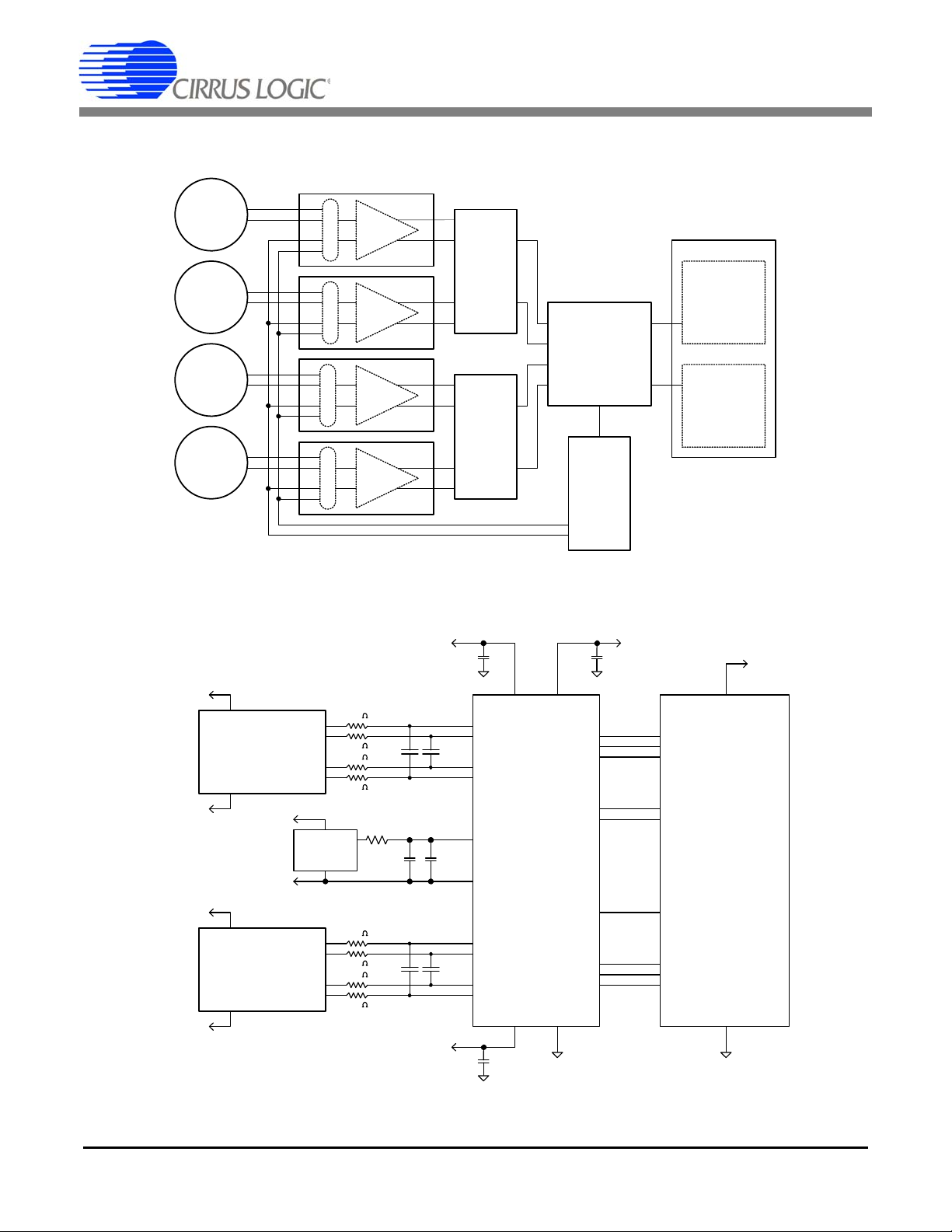
2. SYSTEM DIAGRAM
CS5372A
ΔΣ Modulator
INF+
INR+
INFINR-
INF-
INR-
INF+
INR+
VREF+
VREF-
VA+
VA-VDGND
MDATA1
MFLAG1
MDATA2
MFLAG2
MCLK
MSYNC
PWDN1
OFST
PWDN2
VREF
2.5 V
VA+
VA-
10 Ω
0.01μF
VD
CS5376A
Digital Filter
VDD2
GND
MDATA1
MFLAG1
MDATA2
MFLAG2
MCLK
MSYNC
GPIO
GPIO
GPIO
VA+
0.1μF 0.01μF
VD
VA-
0.1μF
20nF
C0G
20nF
C0G
680
CS3301A
CS3302A
AMPLIFIER
OUTR+
OUTF+
OUTFOUTR-
680
680
680
20nF
C0G
20nF
C0G
680
CS3301A
CS3302A
AMPLIFIER
OUTR+
OUTF+
OUTFOUTR-
680
680
680
VA+
VA+
VA-
VA-
VA+
VA+
VA-
VA-
100μF
Figure 9. Connection Diagram
Differential
Sensor
Differential
Sensor
Differential
Sensor
Differential
Sensor
ΔΣ
Modulator
CS5371A
ΔΣ
Modulator
CS5371A
Digital Filter
CS5376A
Test
DAC
μController
or
Configuration
EEPROM
System
Telemetry
AMP
M
U
X
CS3301A
CS3302A
AMP
M
U
X
AMP
M
U
X
AMP
M
U
X
CS4373A
CS3301A
CS3302A
CS3301A
CS3302A
CS3301A
CS3302A
CS5372A
CS5372A
Figure 8. System Block Diagram
CS5371A CS5372A
DS748F3 13
Page 14

CS5371A CS5372A
Clock
Generator
INF1+
VREF+
VREF-
VA+
VA-
VD
GND
PWDN1
MFLAG1
MDATA1
MCLK
MSYNC
MFLAG2
MDATA2
PWDN2
INF1INR1-
INR1+
INF2+
INF2INR2-
INR2+
4th Order
ΔΣ Modulator
4th Order
ΔΣ Modulator
OFST
CS5372A
Clock
Generator
INF+
VREF+
VREF-
VA+
VA-
VD
GND
PWDN
MFLAG
MDATA
MCLK
MSYNC
INFINR-
INR+
4th Order
ΔΣ Modulator
OFST
CS5371A
Figure 10. CS5371A and CS5372A Block Diagrams
3. MODULATOR OPERATION
The CS5371A and CS5372A are one- and
two-channel, fourth-order ΔΣ modulators optimized for extremely high-resolution measurement of signals between DC and 2000 Hz.
When combined with CS3301A / CS3302A differential amplifiers, the CS4373A test DAC
and CS5376A digital filter, a small, low-power,
self-testing, high-accuracy, multi-channel
measurement system results.
The CS5371A and CS5372A modulators have
high dynamic range and low total harmonic
distortion with very low power consumption
and are optimized for extremely high-resolution measurement of 5 V
tial signals. They convert analog input signals
from the CS3301A / CS3302A differential amplifiers to an oversampled serial bit stream at
512 kbits per second which is then passed to
the digital filter.
The companion CS5376A digital filter generates the clock and synchronization inputs for
14 DS748F3
or smaller differen-
p-p
the CS5371A / CS5372A modulators while receiving the one-bit data and over-range flag
outputs. The digital filter decimates the modulator’s oversampled output bit stream to a
high-resolution, 24-bit output at the selected
output word rate.
3.1 One’s Density
In normal operation a differential analog input
signal is converted to an oversampled ΔΣ serial bit stream on the MDATA output, with a
one’s density proportional to the differential
amplitude of the analog input signal.
One’s density of the MDATA output is defined
as the ratio of ‘1’ bits to total bits in the serial
bit stream output, i.e. an 86% one’s density
has, on average, a ‘1’ value in 86 of every 100
output data bits. The MDATA output has a
nominal 50% one’s density for a mid-scale differential input, approximately 86% one’s density for a positive full-scale input signal, and
approximately 14% one’s density for a negative full-scale input signal.
Page 15

3.2 Decimated 24-bit Output
Table 1. 24-Bit Output Coding for the CS5371A
and CS5372A Modulator and CS5376A Digita l
Filter Combination
Modulator
Differential
Analog Input
Signal
CS5376A Digital Filter
24-Bit Output Code
Offset
Corrected
-60 mV
Offset
-35 mV
Offset
> + (VREF+5%) Error Flag Possible
+ VREF 5D1420 5AD840 5BC688
0 V 000000 FDC420 FEB268
- VREF A2EBE0 A527C0 A43978
> - (VREF+5%) Error Flag Possible
When the CS5371A and CS5372A modulator
operates with the CS5376A digital filter, the final decimated, 24-bit, full-scale output code
range depends if digital offset correction is enabled. With digital offset correction enabled
within the digital filter, amplifier offset and the
modulator internal offset are removed from the
final conversion result.
3.3 Synchronization
The modulator is designed to operate synchronously with other modulators in a distributed
measurement network, so a rising edge on the
MSYNC input resets the internal conversion
state machine to synchronize analog sample
timing. MSYNC is automatically generated by
the CS5376A digital filter after receiving a synchronization signal from the external system,
and is chip-to-chip accurate within ± 1 MCLK
period.
CS5371A CS5372A
3.4 Idle Tones
The CS5371A and CS5372A are delta-sigmatype modulators and so can produce “idle
tones” in the measurement bandwidth when
the differential input signal is a steady-state
DC signal near mid-scale. Idle tones result
from low-frequency patterns in the output data
stream and appear in the measurement spectrum as small tones about -13 5 dB do wn f ro m
full scale.
If the OFST pin is pulled high, idle tones are
eliminated within the modulator by adding
-60 mV (channel 1 of CS5371A and CS5372A)
or -35 mV (channel 2 of CS5372A) of internal
differential offset during conversion to push
idle tones out of the measurement bandwidth.
Care should be taken to ensure external offset
voltages do not negate the internally added
differential offset, or idle tones will re-appear.
3.5 Stability
The CS5371A and CS5372A ΔΣ modulators
have a fourth-order architecture which is conditionally stable and may go into an oscillatory
condition if the analog inputs are over-ranged
more than 5% past either positive or negative
full scale.
If an unstable condition is detected, the modulator collapses to a first-order system and transitions the MFLAG output low-to-high to signal
an error condition to the CS5376A digital filter.
The analog input signal must be reduced to
within the full-scale range for at least 32 MCLK
cycles for the modulator to recover from an oscillatory condition. If the analog input remains
over-ranged for an extended period, the modulator will cycle between fourth-order and firstorder operation and the MFLAG output will be
seen to pulse.
DS748F3 15
Page 16

CS5371A CS5372A
CS5372A
ΔΣ Modulator
INF+
INR+
INFINR-
INF-
INR-
INF+
INR+
VREF+
VREF-
VA+
VA-VDGND
MDATA1
MFLAG1
MDATA2
MFLAG2
MCLK
MSYNC
PWDN1
OFST
PWDN2
VREF
2.5 V
VA+
VA-
10 Ω
0.01μF
VD
CS5376A
Digital Filter
VDD2
GND
MDATA1
MFLAG1
MDATA2
MFLAG2
MCLK
MSYNC
GPIO
GPIO
GPIO
VA+
0.1μF 0.01μF
VD
VA-
0.1μF
20nF
C0G
20nF
C0G
680
CS3301A
CS3302A
AMPLIFIER
OUTR+
OUTF+
OUTFOUTR-
680
680
680
20nF
C0G
20nF
C0G
680
CS3301A
CS3302A
AMPLIFIER
OUTR+
OUTF+
OUTFOUTR-
680
680
680
VA+
VA+
VA-
VA-
VA+
VA+
VA-
VA-
100μF
Figure 11. Analog Signals
• MCLK = 2.048 MHz
• INR± Internal Input Capacitor = 20 pF
• Impedance = [1 / (2.048 MHz * 20 pF)] = 24 kΩ.
4. ANALOG SIGNALS
The CS5371A and CS5372A modulators have
differential analog inputs which are separated
into rough and fine charge differential pairs
(INR±, INF±) to maximize sampling accuracy.
Both sets of modulator inputs require a simple
differential anti-alias RC filter to ensure highfrequency signals do not alias into the measurement bandwidth.
4.1 INR±, INF± Modulator Inputs
The modulator analog inputs are separated
into differential rough and fine signals (INR±,
INF±). The positive half of the differential input
signal is connected to INR+ and INF+, while
the negative half is attached to INF- and INR-.
The INR± pins are switched-capacitor ‘rough
charge’ inputs that pre-charge the internal analog sampling capacitor before it is connected
to the INF± fine input pins.
16 DS748F3
4.2 Input Impedance
The modulator inputs have a dynamic
switched-capacitor architecture and so have a
rough charge input impedance that is inversely
proportional to the input master clock frequency and the input capacitor size, [1 / (f x C)].
Internal to the modulator, the rough inputs
(INR±) pre-charge the sampling capacitor
used by the fine inputs (INF±), therefore the input current to the fine inputs is typically very
low and the effective input impedance is orders of magnitude above the impedance of the
rough inputs.
Page 17

CS5371A CS5372A
• MCLK Frequency = 2.048 MHz
• Sampling Frequency = MCLK / 4 = 512 kHz
• -3 dB Filter Corner = Sampling Freq / 64 = 8 kHz
• RC filter = 1 / [ 2π x(2xR
series
)xC
diff
] ~ 8 kHz
4.3 Anti-alias Filter
The modulator inputs are required to be bandwidth limited to ensure modulator loop stability
and prevent high-frequency signals from aliasing into the measurement bandwidth. The use
of simple, single-pole, differential, low-pass
RC filters across the INR± and INF± inputs ensures high-frequency signals are rejected before they can alias into the measurement
bandwidth.
The CS3301A / CS3302A differential amplifiers are designed with separate rough and fine
analog outputs (OUTR±, OUTF±) that match
the modulator rough and fine inputs (INR±,
INF±). External anti-alias series resistors and
external differential capacitors are required to
create the anti-alias RC filters.
The approximate -3 dB corner of the input antialias filter is nominally set to the internal analog sampling rate divided by 64, which itself is
a division by 4 of the MCLK rate.
ing X7R-type capacitors on the fine analog inputs will significantly degrade total harmonic
distortion performance.
4.4 Analog Differential Signals
Differential analog signals into the CS5371A
and CS5372A consist of two halves with equal
but opposite magnitude varying about a common mode voltage. A full-scale, 5 V
P-P
, differential signal centered on a -0.15 V common
mode voltage will have:
SIG+ = -0.15 V + 1.25 V = +1.1 V
SIG- = -0.15 V - 1.25 V = -1.4 V
SIG+ is +2.5 V relative to SIG-
For the opposite case:
SIG+ = -0.15 V - 1.25 V = -1.4 V
SIG- = -0.15 V + 1.25 V = +1.1 V
SIG+ is -2.5 V relative to SIG-
So the total swing for SIG+ relative to SIG- is
(+2.5 V) – (-2.5 V) = 5 V
differential. A simi-
p-p
lar calculation can be done for SIG- relative to
SIG+.
Figure 9 on page 13 illustrates the CS5371A and
CS5372A modulator analog connections with
input anti-alias filter components. Filter components on the rough and fine pins should be
identical values for optimum performance, with
the capacitor values a minimum of 0.02 μF.
The rough input can use either X7R- or C0Gtype capacitors, while the fine input requires
C0G-type capacitors for optimal linearity. Us-
DS748F3 17
It’s important to note that a 5 V
differential
p-p
signal centered on a -0.15 V common mode
voltage never exceeds +1.1 V with respect to
ground and never drops below -1.4 V with respect to ground on either half. By definition,
differential voltages are measured with respect to the opposite half, not relative to
ground. A voltmeter differentially measuring
between SIG+ and SIG- in the above example
would correctly read 1.767 V
rms
, or 5 V
p-p
.
Page 18

CS5371A CS5372A
CS5372A
ΔΣ Modulator
INF+
INR+
INFINR-
INF-
INR-
INF+
INR+
VREF+
VREF-
VA+
VA-VDGND
MDATA1
MFLAG1
MDATA2
MFLAG2
MCLK
MSYNC
PWDN1
OFST
PWDN2
VREF
2.5 V
VA+
VA-
10 Ω
0.01μF
VD
CS5376A
Digital Filter
VDD2
GND
MDATA1
MFLAG1
MDATA2
MFLAG2
MCLK
MSYNC
GPIO
GPIO
GPIO
VA+
0.1μF 0.01μF
VD
VA-
0.1μF
20nF
C0G
20nF
C0G
680
CS3301A
CS3302A
AMPLIFIER
OUTR+
OUTF+
OUTFOUTR-
680
680
680
20nF
C0G
20nF
C0G
680
CS3301A
CS3302A
AMPLIFIER
OUTR+
OUTF+
OUTFOUTR-
680
680
680
VA+
VA+
VA-
VA-
VA+
VA+
VA-
VA-
100μF
Figure 12. Digital Signals
5. DIGITAL SIGNALS
The CS5371A and CS5372A modulators are
designed to operate with the CS5376A digital
filter. The digital filter generates the modulator
clock and synchronization signals (MCLK and
MSYNC) while receiving back the modulator
one-bit ΔΣ conversion data and over-range
flag (MDATA and MFLAG).
5.1 MCLK Connection
The CS5376A digital filter generates the master clock for CS5371A and CS5372A, typically
2.048 MHz, from a synchronous clock input
from the external system. If MCLK is disabled
during operation, the modulators will enter a
power down state after approximately 40 µS.
By default, MCLK is disabled at reset and is
enabled by writing the digital filter CONFIG
register.
MCLK must have low jitter to guarantee full analog performance, requiring a crystal- or
VCXO-based system clock input to the digital
18 DS748F3
filter. Clock jitter on the digital filter CLK input
directly translates to jitter on MCLK.
5.2 MSYNC Connection
The CS5376A digital filter also provides a synchronization signal to the CS5371A and
CS5372A modulators. The MSYNC signal is
automatically generated following a rising
edge received on the digital filter SYNC input.
By default, MSYNC generation is disabled at
reset and is enabled by writing the digital filter
CONFIG register.
The input SYNC signal to the CS5376A digital
filter sets a common reference time t0 for measurement events, thereby synchronizing analog sampling across a measurement network.
The timing accuracy of the received SYNC signal from measurement node to measurement
node must be ±1 MCLK to maximize the
MSYNC analog sample synchronization accuracy.
Page 19

CS5371A CS5372A
The CS5371A and CS5372A MSYNC input is
rising-edge triggered and resets the internal
MCLK counter/divider to guarantee synchronous operation with other system devices.
While the MSYNC signal synchronizes the internal operation of the modulators, by default,
it does not synchronize the phase of the sine
wave from the CS4373A test DAC unless enabled in the digital filter TBSCFG register.
5.3 MDATA Connection
During normal operation the CS5371A and
CS5372A modulators output a ΔΣ serial bit
stream to the MDATA pin, with a one’s density
proportional to the differential amplitude of the
analog input signal. The output bit rate from
the MDATA output is a divide-by-four of the input MCLK, and so is nominally 512 kHz.
The MDATA output has a 50% one’s density
for a mid-scale analog input, approximately
86% one’s density for a positive full-scale analog input, and approximately 14% one’s density for a negative full-scale analog input. One’s
density of the MDATA output is defined as the
ratio of ‘1’ bits to total bits in the serial bit
stream output; i.e. an 86% one’s density has,
on average, a ‘1’ value in 86 of every 100 output data bits.
5.4 MFLAG Connection
The CS5371A and CS5372A ΔΣ modulators
have a fourth-order architecture which is conditionally stable and may go into an oscillatory
condition if the analog inputs are over-ranged
more than 5% past either positive or negative
full-scale.
When an unstable condition is detected, the
modulator automatically collapses to a first-order system to regain stability and then transitions the MFLAG output low-to-high to signal
an error condition to the CS5376A digital filter.
The MFLAG output connects to a dedicated input on the digital filter, causing an error flag to
be set in the status byte of the next output data
word.
For the modulator to recover from an unstable
condition, the analog input signal must be reduced to within the full-scale input range for at
least 32 MCLK cycles. If the analog input remains over-ranged for an extended period, the
modulator will cycle between fourth-order and
first-order operation and the MFLAG output
will be seen to pulse.
5.5 OFST Connection
The CS5376A controls 12 general-purpose input output (GPIO) pins through the digital filter
GPCFG register. These GPIO pins can be assigned to operate the CS5371A and CS5372A
OFST and PWDN pins.
If the OFST pin is pulled high, idle tones are
eliminated within the modulator by adding
-60 mV (channel 1 of CS5371A and CS5372A)
or -35 mV (channel 2 of CS5372A) of internal
differential offset during conversion to push
idle tones out of the measurement bandwidth.
Care should be taken to ensure external offset
voltages do not negate the internally added
differential offset, or idle tones will re-appear.
DS748F3 19
Page 20

6. POWER MODES
NORMAL OPERATION
MCLK = ON
PWDN = 0
POWER DOWN
MCLK = ON
PWDN = 1
POWER DOWN
MCLK = OFF
PWDN = X
Figure 13. Power Mode Diagram
CS5371A CS5372A
The CS5371A and CS5372A modulators have
three power modes. Normal operation, power
down with MCLK enabled, and power down
with MCLK disabled.
6.1 Normal Operation
With MCLK active and the PWDN pin driven
low, the CS5371A and CS5372A modulators
perform normal data acquisition. A differential
analog input signal is converted to an oversampled 1-bit ΔΣ bit stream at 512 kHz. This ΔΣ
bit stream is then digitally filtered and decimated by the CS5376A device to a high-precision
24-bit output.
6.2 Power Down, MCLK Enabled
With MCLK active and the PWDN pin driven
high, the CS5371A and CS5372A modulators
are placed into a power-down state. During
this power-down state the modulators are disabled and all outputs are high impedance.
6.3 Power Down, MCLK Disabled
If MCLK is stopped, an internal loss-of-clock
detection circuit automatically places the
CS5371A and CS5372A into a power-down
state. This power-down state is independent of
the PWDN pin setting and is automatically invoked after approximately 40 μs without receiving an incoming MCLK edge.
During this power-down state, the modulators
are disabled and all outputs are high impedance. When used with the CS5376A digital filter, the CS5371A and CS5372A are in this
power-down state immediately after reset
since MCLK is disabled by default.
20 DS748F3
Page 21

7. VOLTAGE REFERENCE
10
Ω
To VREF+
+
From VA+
Regulator
2.500 V
VREF
0.1 μF
To VREF-
0.1 μF
100 μF
0.1 μF
0.1 μF
0.1 μF
100 μF
100 μF
From VARegulator
Route VREF± as a differential pair
from the 100uF RC filter capacitor
Figure 14. Voltage Reference Circuit
CS5371A CS5372A
The CS5371A and CS5372A modulators require a 2.500 V precision voltage reference to
be supplied to the VREF± pins.
7.1 VREF Power Supply
To guarantee proper regulation headroom for
the voltage reference device, the voltage reference GND pin should be connected to VA- instead of system ground, as shown in
Figure 14. This connection results in a VREF-
voltage equal to VA- and a VREF+ voltage
very near ground [(VA-) + 2.500 VREF].
Power supply inputs to the voltage reference
device should be bypassed to system ground
with 0.1 μF capacitors placed as close as possible to the power and ground pins. In addition
to 0.1 μF local bypass capacitors, at least
100 μF of bulk capacitance to system ground
should be placed on each power supply near
the voltage regulator outputs. Bypass capacitors should be X7R, C0G, tantalum, or other
high-quality dielectric type.
ence output. By sharing a common RC filter,
signal-dependent sampling of the voltage reference by one system device could cause unwanted tones to appear in the measurement
bandwidth of another system device via common impedance coupling.
7.3 VREF PCB Routing
To minimize the possibility of outside noise
coupling into the CS5371A and CS5372A voltage reference input, the VREF± traces should
be routed as a differential pair from the large
capacitor of the voltage reference RC filter.
Careful control of the voltage reference source
and return currents by routing VREF± as a differential pair will significantly improve immunity from external noise.
To further improve noise rejection of the
VREF
pass
± differential route, include 0.1 μF by-
capacitors to system ground as close as
possible to the VREF+ and VREF- pins of the
CS5371A and CS5372A.
7.2 VREF RC Filter
A primary concern in selecting a precision voltage reference device is noise performance in
the measurement bandwidth. The Linear
Technology LT1019AIS8-2.5 voltage refer-
ence yields acceptable noise levels if the output is filtered with a low-pass RC filter.
A separate RC filter is required for each system device connected to a given voltage refer-
DS748F3 21
7.4 VREF Input Impedance
The switched-capacitor input architecture of
the VREF
± inputs results in an input imped-
ance that depends on the internal capacitor
size and the MCLK frequency. With a 15 pF internal capacitor and a 2.048 MHz MCLK, the
VREF input impedance is approximately
1 / [(2.048 MHz) x (15 pF)] = 32 kΩ. While the
size of the internal capacitor is fixed, the volt-
Page 22

CS5371A CS5372A
age reference input impedance will vary with
MCLK.
The voltage reference external RC filter series
resistor creates a voltage divider with the
VREF input impedance to reduce the effective
applied input voltage. To minimize gain error
resulting from this voltage divider effect, the
RC filter series resistor should be the minimum
size recommended in the voltage reference
device data sheet.
7.5 VREF Accuracy
The nominal voltage reference input is specified as 2.500 V across the VREF
CS5371A and CS5372A gain accuracy speci-
± pins, and all
fications are measured using a nominal voltage reference input. Any variation from a
nominal VREF input will proportionally vary the
analog full-scale gain accuracy.
Since temperature drift of the voltage reference results in gain drift of the analog full-scale
amplitude, care should be taken to minimize
temperature drift effects through careful selection of passive components and the voltage
reference device itself. Gain drift specifications
of the CS5371A and CS5372A do not include
the temperature drift effects of external passive components or of the voltage reference
device itself.
22 DS748F3
Page 23

8. POWER SUPPLIES
CS5371A
CS5372A
VA+ VD
VA- GND
0.1 uF 100 uF0.1 uF100 uF
100 uF
0.1 uF
To VA+
Regulator
To VA-
Regulator
To VD
Regulator
Figure 15. Power Supply Diagram
CS5371A CS5372A
The CS5371A and CS5372A modulators have
a positive analog power supply pin (VA+), a
negative analog power supply pin (VA-), a digital power supply pin (VD), and a ground pin
(GND).
For proper operation, power must be supplied
to all power supply pins, and the ground pin
must be connected to system ground. The
CS5371A and CS5372A digital power supply
(VD) and the CS5376A digital power supply
(VDD) must share a common voltage.
8.1 Power Supply Bypassing
The VA+, VA-, and VD power supplies should
be bypassed to system ground with 0.1 μF capacitors placed as close as possible to the
power pins of the device. In addition to the
0.1 μF local bypass capacitors, at least 100 μF
bulk capacitance to system ground should be
placed on each power supply near the voltage
regulator output, with additional power supply
bulk capacitance placed among the analog
component route if space permits. Bypass capacitors should be X7R, C0G, tantalum, or
other high-quality dielectric type.
8.2 PCB Layers and Routing
The CS5371A and CS5372A are high-performance devices, and special care must be taken to ensure power and ground routing is
correct. Power can be supplied either through
dedicated power planes or routed traces.
DS748F3 23
When routing power traces, it is recommended
to use a “star” routing scheme with the star
point either at the voltage regulator output or at
a local power supply bulk capacitor.
It is also recommended to dedicate a full PCB
layer to a solid ground plane, without splits or
routing. All bypass capacitors should connect
between the power supply circuit and the solid
ground plane as near as possible to the device
power supply pins.
The CS5371A and CS5372A analog signals
are differentially routed and do not normally require connection to a separate analog ground.
However, if a separate analog ground is required, it should be routed using a “star” routing scheme on a separate layer from the solid
ground plane and connected to the ground
plane only at a single point. Be sure all active
devices and passive components connected
to the separate analog ground are included in
the “star” route to ensure sensitive analog currents do not return through the ground plane.
8.3 Power Supply Rejection
Power supply rejection of the CS5371A and
CS5372A is frequency dependent. The
CS5376A digital filter fully rejects power supply noise for frequencies above the selected
digital filter corner frequency. Power supply
noise frequencies between DC and the digital
filter corner frequency are rejected as specified in the Power Supply Characteristics table.
Page 24

CS5371A CS5372A
8.4 SCR Latch-up Considerations
It is recommended to connect the VA- power
supply to system ground (GND) with a reverse-biased Schottky diode. At power up, if
the VA+ power supply ramps up before the
VA- supply is established, the VA- pin voltage
could be pulled above ground potential
through the CS5371A and CS5372A device. If
the VA- supply is pulled 0.7 V or more above
GND, SCR latch-up can occur. A reverse-biased Schottky diode will clamp the VA- voltage
a maximum of 0.3 V above ground to ensure
SCR latch-up does not occur at power up.
8.5 DC-DC Converters
Many low-frequency measurement systems
are battery powered and utilize DC-DC converters to efficiently generate power supply
voltages. To minimize interference effects, operate the DC-DC converter at a frequency
which is rejected by the digital filter, or operate
it synchronous to the MCLK rate.
A synchronous DC-DC converter whose operating frequency is derived from MCLK will theoretically minimize the potential for “beat
frequencies” to appear in the measurement
bandwidth. However this requires the source
clock to remain jitter free within the DC-DC
converter circuitry. If clock jitter can occur within the DC-DC converter (as in a PLL-based architecture), it’s better to use a nonsynchronous DC-DC converter whose switching frequency is rejected by the digital filter.
During PCB layout, do not place high-current
DC-DC converters near sensitive analog components. Carefully routing a separate DC-DC
“star” ground will help isolate noisy switching
currents away from the sensitive analog components.
24 DS748F3
Page 25

9. PIN DESCRIPTION - CS5371A
1
2
3
4
5
6
7
817
18
19
20
21
22
23
24
9
10
11
12 13
14
15
16
Rough Non-Inverting Input INR+
Fine Non-Inverting Input INF+
Fine Inverting Input INF-
Rough Inverting Input INR-
Positive Voltage Reference Input VREF+
Negative Voltage Reference Input VREF-
Negative Analog Power Supply VA-
Positive Analog Power Supply VA+
No Internal Connection NC
No Internal Connection NC
No Internal Connection NC
No Internal Connection NC
PWDN Power-down Enable
GND Digital Ground
MFLAG Modulator Flag Output
MDATA Modulator Data Output
MSYNC Modulator Sync Input
MCLK Modulator Clock Input
VD Positive Digital Power Supply
GND Digital Ground
NC No Internal Connection
NC No Internal Connection
OFST Offset Mode Select
VD Positive Digital Power Supply
CS5371A CS5372A
Power Supplies
VA+ _ Positive Analog Power Supply, pin 8
VA- _ Negative Analog Power Supply, pin 7
VD _ Positive Digital Power Supply, pin 13, 18
GND _ Ground, pin 17, 23
Analog Inputs
INR+ _ Rough Non-Inverting Input, pin 1
Rough non-inverting analog input. The rough input settles non-linear currents to improve
linearity on the fine input and reduce harmonic distortion.
INF+ _ Fine Non-Inverting Input, pin 2
INF- _ Fine Inverting Input, pin 3
INR- _ Rough Inverting Input, pin 4
DS748F3 25
Fine non-inverting analog input.
Fine inverting analog input.
Rough inverting analog input. The rough input settles non-linear currents to improve linearity
on the fine input and reduce harmonic distortion.
Page 26

VREF+ _ Positive Voltage Reference Input, pin 5
Input for an external +2.500 V voltage reference relative to VREF-.
VREF- _ Negative Voltage Reference Input, pin 6
This pin should be tied to VA- near the voltage reference output.
Digital Inputs
MCLK _ Modulator Clock Input, pin 19
A CMOS compatible clock input for the modulator internal master clock, nominally 2.048 MHz
with an amplitude equal to the VD digital power supply.
MSYNC _ Modulator Sync Input, pin 20
A low to high transition resets the internal clock phasing of the modulator. This assures the
sampling instant and modulator data output are synchronous to the external system.
OFST _ Offset Mode Select, pin 14
When high, adds approximately -60 mV or -35 mV of internal differential offset to the analog
input signal to guarantee any ΔΣ idle tones are removed. When low, no offset is added.
CS5371A CS5372A
PWDN _ Power-down Mode, pin 24
When high, the modulator is in power-down mode. Halting MCLK while in power down mode
reduces modulator power dissipation further.
Digital Outputs
MDATA _ Modulator Data Output, pin 21
Modulator data is output as a 1-bit serial data stream at 512 kHz with an MCLK input of
2.048 MHz.
MFLAG _ Modulator Flag Output, pin 22
A high level output indicates the modulator is unstable due to an over-range on the analog
inputs.
26 DS748F3
Page 27

10. PIN DESCRIPTION - CS5372A
1
2
3
4
5
6
7
817
18
19
20
21
22
23
24
9
10
11
12 13
14
15
16
Ch. 1 Rough Non-Inverting Input INR1+
Ch. 1 Fine Non-Inverting Input INF1+
Ch. 1 Fine Inverting Input INF1-
Ch. 1 Rough Inverting Input INR1-
Positive Voltage Reference Input VREF+
Negative Voltage Reference Input VREF-
Negative Analog Power Supply VA-
Positive Analog Power Supply VA+
Ch. 2 Rough Inverting Input INR2-
Ch. 2 Fine Inverting Input INF2-
Ch. 2 Fine Non-Inverting Input INF2+
Ch. 2 Rough Non-Inverting Input INR2+
PWDN1 Ch. 1 Power-down Enable
GND Digital Ground
MFLAG1 Ch. 1 Modulator Flag Output
MDATA1 Ch. 1 Modulator Data Output
MSYNC Modulator Sync Input
MCLK Modulator Clock Input
VD Positive Digital Power Supply
GND Digital Ground
MDATA2 Ch. 2 Modulator Data Output
MFLAG2 Ch. 2 Modulator Flag Output
OFST Offset Mode Select
PWDN2 Ch. 2 Power-down Enable
CS5371A CS5372A
Power Supplies
VA+ _ Positive Analog Power Supply, pin 8
VA- _ Negative Analog Power Supply, pin 7
VD _ Positive Digital Power Supply, pin 18
GND _ Ground, pin 17, 23
Analog Inputs
INR1+, INR2+ _ Channel 1 & 2 Rough Non-Inverting Inputs, pin 1, 12
Rough non-inverting analog inputs. The rough inputs settle non-linear currents to improve
linearity on the fine inputs and reduce harmonic distortion.
INF1+, INF2+ _ Channel 1 & 2 Fine Non-Inverting Input, pin 2, 11
INF1-, INF2- _ Channel 1 & 2 Fine Inverting Input, pin 3, 10
INR1-, INR2- _ Channel 1 & 2 Rough Inverting Inputs, pin 4, 9
DS748F3 27
Fine non-inverting analog inputs.
Fine inverting analog inputs.
Rough inverting analog inputs. The rough inputs settle non-linear currents to improve linearity
on the fine inputs and reduce harmonic distortion.
Page 28

VREF+ _ Positive Voltage Reference Input, pin 5
Input for an external +2.5 V voltage reference relative to VREF-.
VREF- _ Negative Voltage Reference Input, pin 6
This pin should be tied to VA- near the voltage reference output.
Digital Inputs
MCLK _ Modulator Clock Input, pin 19
A CMOS compatible clock input for the modulator internal master clock, nominally 2.048 MHz
with an amplitude equal to the VD digital power supply.
MSYNC _ Modulator Sync Input, pin 20
A low to high transition resets the internal clock phasing of the modulator. This assures the
sampling instant and modulator data output are synchronous to the external system.
OFST _ Offset Mode Select, pin 14
When high, adds approximately -60 mV or -35 mV of internal differential offset to the analog
input signal to guarantee any ΔΣ idle tones are removed. When low, no offset is added.
CS5371A CS5372A
PWDN1, PWDN2 _ Channel 1 & 2 Power-down Mode, pin 24, 13
When high, the modulator is in power down mode. Halting MCLK while in power down mode
reduces modulator power dissipation further.
Digital Outputs
MDATA1, MDATA2 _ Modulator Data Output, pin 21, 16
Modulator data is output as a 1-bit serial data stream at 512 kHz with an MCLK input of
2.048 MHz.
MFLAG1, MFLAG2 _ Modulator Flag, pin 22, 15
A high level output indicates the modulator is unstable due to an over-range on the analog
inputs.
28 DS748F3
Page 29
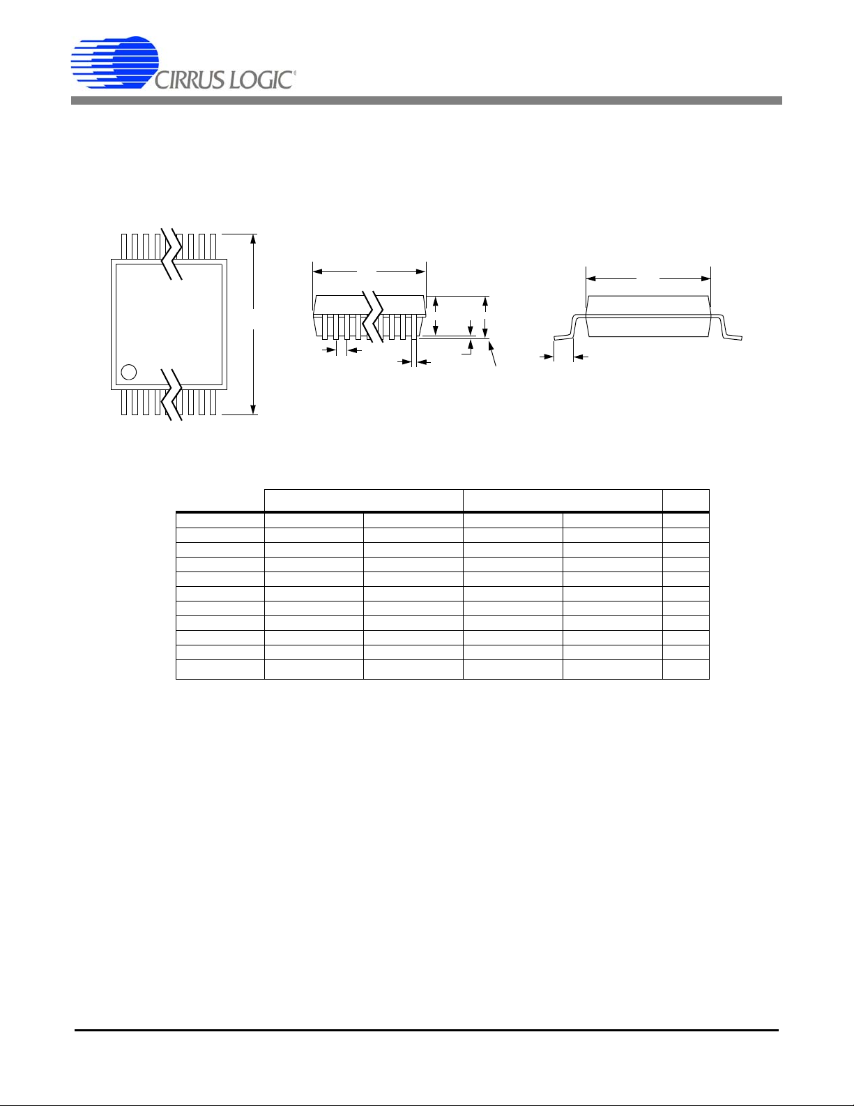
11.PACKAGE DIMENSIONS
24 PIN SSOP PACKAGE DRAWING
E
N
1
23
e
b
2
A1
A2
A
D
SEATING
PLANE
E1
1
L
SIDE VIEW
END VIEW
TOP VIEW
CS5371A CS5372A
INCHES MILLIMETERS
DIM MIN MAX MIN MAX
A -- 0.084 -- 2.13
A1 0.002 0.010 0.05 0.25
A2 0.064 0.074 1.62 1.88
b 0.009 0.015 0.22 0.38 2,3
D 0.311 0.335 7.90 8.50 1
E 0.291 0.323 7.40 8.20
E1 0.197 0.220 5.00 5.60 1
e 0.024 0.027 0.61 0.69
L 0.025 0.040 0.63 1.03
∝
0° 8° 0° 8°
NOTE
Notes: 1. “D” and “E1” are reference datums and do not in cluded mold flash or protrusions, but do include mold
mismatch and are measured at the parting line, mold flash or protrusions shall not exceed 0.20 mm per
side.
2. Dimension “b” does not include dambar protrusion/intrusion. Allowable dambar protrusion shall be
0.13 mm total in excess of “b” dimension at maximum material condition. Dambar intrusion shall not
reduce dimension “b” by more than 0.07 mm at least material condition.
3. These dimensions apply to the flat section of the lead between 0.10 and 0.25 mm from lead tips.
DS748F3 29
Page 30

12. ORDERING INFORMATION
Model Temperature Package
CS5371A-ISZ (lead free)
-40 to +85 °C 24-pin SSOP
CS5372A-ISZ (lead free)
CS5371A CS5372A
30 DS748F3
Page 31

CS5371A CS5372A
13.ENVIRONMENTAL, MANUFACTURING, & HANDLING INFORMATION
Model Number Peak Reflow Temp MSL Rating* Max Floor Li fe
CS5371A-ISZ (lead free)
CS5372A-ISZ (lead free)
* MSL (Moisture Sensitivity Level) as specified by IPC/JEDEC J-STD-020.
260 °C 3 7 Days
DS748F3 31
Page 32

CS5371A CS5372A
Contacting Cirrus Logic Support
For all product questions and inquiries contact a Cirrus Logic Sales Representative.
To find the one nearest to you go to www.cirrus.com
IMPORTANT NOTICE
Cirrus Logic, Inc. and its subsidiaries ("Cirrus") believe that the information contained in this document is accur at e and rel i a b l e. Howeve r, th e inf ormat i on is sub jec t
to change without noti ce and is p rovided " AS IS" wi thout war ranty of any kind (express or impli ed). Cust omers are advised to obtain the latest version of relevant
information to verify, before placing orders, that information being relied on is current and complete. All products are sold subject to the terms and conditions of sale
supplied at the time of order acknowledgm ent, including tho se pertaining to war ranty, indemn ification, and lim itation of liability. No responsibility is assumed by Cirrus
for the use of this information, including use of this information as the basis for manufacture or sale of any items, or for infringement of patents or other rights of third
parties. This document is the property of Cirrus and by furnishing this information, Cirrus grants no license, express or implied under any patents, mask work rights,
copyrights, trademarks, trade secrets or other intellectual property rights. Cirrus owns the copyrights associated with the information contained herein and gives consent for copies to be made of the info rmation only for use within your organization with respect to Cirrus integrated circuits or other products of Cirrus. This consent
does not extend to other copying such as copying for general distribution, advertising or promotional purposes, or for creating any work for resale.
CERTAIN APPLICATIONS USING SEMICONDUCTOR PRODUCTS MAY INVOLVE POTENTIAL RISK S OF DEA TH, PERSONAL INJURY, OR SEVERE PROPERTY OR ENVIRONMENTAL DAMAGE ("CRITICAL APPLICATIONS"). CIRRUS PRODUCTS ARE NOT DESIGNED, AUTHORIZED OR WARRANTED FOR USE
IN AIRCRAFT SYSTEMS, MILITARY APPLICATIONS, PRODUCTS SURGICALLY IMPLANTED INTO THE BODY, AUTOMOTIVE SAFETY OR SECURITY DE-
VICES, LIFE SUPPORT PRODUCTS OR OTHER CRITICAL APPLICATIONS. INCLUSION OF CIRRUS PRODUCTS IN SUCH APPLICATIONS IS UNDERSTOOD
TO BE FULLY AT THE CUSTOMER'S RISK AND CIRRUS DISCLAIMS AND MAKES NO WARRANTY, EXPRESS, STATUTORY OR IMPLIED, INCLUDING THE
IMPLIED WARRANTIES OF MERCHANTABILITY AND FITNESS FOR PARTICULAR PURPOSE, WITH REGARD TO ANY CIRRUS PRODUCT THAT IS USED
IN SUCH A MANNER. IF THE CUSTOMER OR CUSTOMER'S CUSTOMER USES OR PERMITS THE USE OF CIRRUS PRODUCTS IN CRITICAL APPLICATIONS, CUSTOMER AGREES, BY SUCH USE, TO FULLY INDEMNI FY CIRRUS, ITS OFFICERS, DIRECTORS, EMPLOYEES, DISTRIBUTORS AND OTHER
AGENTS FROM ANY AND ALL LIABILITY, IN CLUDING ATTORNEYS' FEES AND COSTS, THAT MAY RESULT F ROM OR ARISE IN CONNECTION WITH
THESE USES.
Cirrus Logic, Cirrus, and the Cirrus Logic logo designs are trademarks of Cirrus Logic, Inc. All other brand and product names in this document may be trademarks
or service marks of their respective owners.
14.REVISION HISTORY
Revision Date Changes
PP1 OCT 2006 Preliminary release.
F1 DEC 2006 Updated to final status with most-recent characterization data for Cirrus QPL pro-
cess.
F2 SEP 2009 P.1 Remove “-112dB THD Maximum” bullet.
P.7 Add typical THD specification for Vcm = (VA-) + 2.35V.
P.7 Add typical Linearity specification for Vcm = (VA-) + 2 .35V.
P.7 Modify note 14 to specify THD at Vcm = (VA-) + 2.50V.
P.7 Add note 15 to specify THD at Vcm = (VA-) + 2.35V.
F3 SEP 2010 Removed references to CS3301/CS3302 as it is EOL.
Removed lead-containing device ordering information.
32 DS748F3
 Loading...