

Page 1
Features
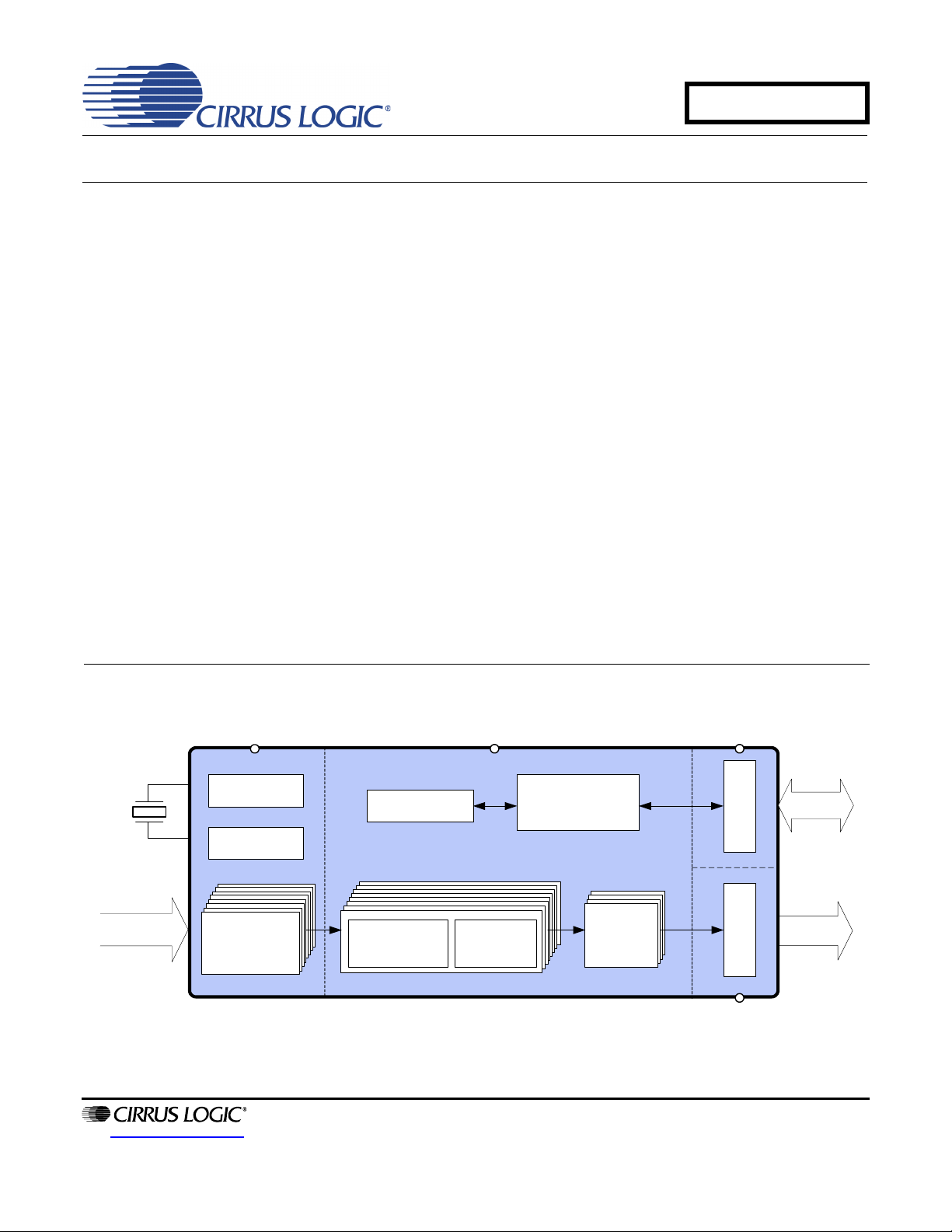
Digital
Audio
Voltage
Reference
Level
Translator
Level
Translator
Internal
Oscillator
VD
3.3 - 5V
Control Interface
I2C, SPI
or Pins
Configuration
Registers
VA
5V
VLC
1.8 - 5V
VLS
1.8 - 5V
8 Differential
Analog Inputs
Device
Control
Serial
Audio Out
PCM or
TDM
Decimation
Filter
High Pass
Filter
Multi-bit
ADC
CS5368
114 dB, 192 kHz, 8-Channel A/D Converter
Advanced Multi-bit Delta-Sigma Architecture
24-Bit Conversion
114 dB Dynamic Range
-105 dB THD+N
Supports Audio Sample Rates up to 216 kHz
Selectable Audio Interface Formats
– Left-Justified, I²S, TDM
– 8-Channel TDM Interface Formats
Low Latency Digital Filter
Less than 680 mW Power Consumption
On-Chip Oscillator Driver
Operation as System Clock Master or Slave
Auto-Detect Speed in Slave Mode
Differential Analog Architecture
Separate 1.8 V to 5 V Logic Supplies for
Control and Serial Ports
High-Pass Filter for DC Offset Calibration
Overflow Detection
Footprint Compatible with the 4-Channel
CS5364 and 6-Channel CS5366
Additional Control Port Features
Supports I²C or SPI™ Control Interface per
specifications on page 17 and page 18
Individual Channel HPF Disable
Overflow Detection for Individual Channels
Mute Control for Individual Channels
Independent Power-Down Control per Channel
Pair
http://www.cirrus.com
Copyright Cirrus Logic, Inc. 2014
(All Rights Reserved)
JUL '14
DS624F5
Page 2

CS5368
Description
The CS5368 is a complete 8-channel analog-to-digital converter for digital audio systems. It performs sampling, analog-to-digital conversion, and anti-alias filtering, generating 24-bit values for all 8-channel inputs in serial form at
sample rates up to 216 kHz per channel.
The CS5368 uses a 5th-order, multi-bit delta sigma modulator followed by low latency digital filtering and decimation, which removes the need for an external anti-aliasing filter. The ADC uses a differential input architecture which
provides excellent noise rejection.
Dedicated level translators for the Serial Port and Control Port allow seamless interfacing between the CS5368 and
other devices operating over a wide range of logic levels. In addition, an on-chip oscillator driver provides clocking
flexibility and simplifies design.
The CS5368 is the industry’s first audio A/D to support a high-speed TDM interface which provides a serial output
of 8 channels of audio data with sample rates up to 216 kHz within a single data stream. It further reduces layout
complexity and relieves input/output constraints in digital signal processors.
The CS5368 is available in a 48-pin LQFP package in both Commercial (-40°C to 85°C) and Automotive grades
(-40°C to +105°C). The CDB5368 Customer Demonstration board is also available for device evaluation and
implementation suggestions. Please see “Ordering Information” on page 41 for complete ordering information.
The CS5368 is ideal for high-end and pro-audio systems requiring unrivaled sound quality, transparent conversion,
wide dynamic range and negligible distortion, such as A/V receivers, digital mixing consoles, multi-channel recorders, outboard converters, digital effect processors, and automotive audio systems.
2 DS624F5
Page 3

TABLE OF CONTENTS
1. PIN DESCRIPTION ................................................................................................................................. 6
2. TYPICAL CONNECTION DIAGRAM ................................................................................................... 9
3. CHARACTERISTICS AND SPECIFICATIONS .................................................................................... 10
RECOMMENDED OPERATING CONDITIONS ................................................................................. 10
ABSOLUTE RATINGS ....................................................................................................................... 10
SYSTEM CLOCKING ......................................................................................................................... 10
DC POWER ........................................................................................................................................ 11
LOGIC LEVELS ................................................................................................................................. 11
PSRR, VQ AND FILT+ CHARACTERISTICS .................................................................................... 11
ANALOG CHARACTERISTICS (COMMERCIAL) .............................................................................. 12
ANALOG CHARACTERISTICS (AUTOMOTIVE) ............................................................................... 13
DIGITAL FILTER CHARACTERISTICS ............................................................................................. 14
OVERFLOW TIMEOUT ...................................................................................................................... 14
SERIAL AUDIO INTERFACE - I²S/LJ TIMING ................................................................................... 15
SERIAL AUDIO INTERFACE - TDM TIMING ..................................................................................... 16
SWITCHING SPECIFICATIONS - CONTROL PORT - I²C TIMING ................................................... 17
SWITCHING SPECIFICATIONS - CONTROL PORT - SPI TIMING .................................................. 18
4. APPLICATIONS ................................................................................................................................... 19
4.1 Power ............................................................................................................................................. 19
4.2 Control Port Mode and Stand-Alone Operation .............................................................................. 19
4.2.1 Stand-Alone Mode ................................................................................................................. 19
4.2.2 Control Port Mode ................................................................................................................. 19
4.3 Master Clock Source ...................................................................................................................... 20
4.3.1 On-Chip Crystal Oscillator Driver .......................................................................................... 20
4.3.2 Externally Generated Master Clock ....................................................................................... 20
4.4 Master and Slave Operation ........................................................................................................... 21
4.4.1 Synchronization of Multiple Devices ......................................................................................21
4.5 Serial Audio Interface (SAI) Format ................................................................................................ 22
4.5.1 I²S and LJ Format .................................................................................................................. 22
4.5.2 TDM Format .......................................................................................................................... 23
4.5.3 Configuring Serial Audio Interface Format ............................................................................ 23
4.6 Speed Modes ................................................................................................................................. 23
4.6.1 Sample Rate Ranges ............................................................................................................ 23
4.6.2 Using M1 and M0 to Set Sampling Parameters .................................................................... 23
4.6.3 Master Mode Clock Dividers ................................................................................................. 24
4.6.4 Slave Mode Audio Clocking With Auto-Detect ...................................................................... 24
4.7 Master and Slave Clock Frequencies ............................................................................................. 25
4.8 Reset .............................................................................................................................................. 27
4.8.1 Power-Down Mode ................................................................................................................ 27
4.9 Overflow Detection ......................................................................................................................... 27
4.9.1 Overflow in Stand-Alone Mode .............................................................................................. 27
4.9.2 Overflow in Control Port Mode .............................................................................................. 27
4.10 Analog Connections ..................................................................................................................... 28
4.11 Optimizing Performance in TDM Mode ........................................................................................29
4.12 DC Offset Control ......................................................................................................................... 29
4.13 Control Port Operation .................................................................................................................. 30
4.13.1 SPI Mode ............................................................................................................................. 30
4.13.2 I²C Mode .............................................................................................................................. 31
5. REGISTER MAP ................................................................................................................................... 32
5.1 Register Quick Reference ............................................................................................................. 32
5.2 00h (REVI) Chip ID Code & Revision Register ............................................................................... 32
CS5368
DS624F5 3
Page 4

5.3 01h (GCTL) Global Mode Control Register ...................................................................................32
5.4 02h (OVFL) Overflow Status Register ........................................................................................... 33
5.5 03h (OVFM) Overflow Mask Register ............................................................................................ 33
5.6 04h (HPF) High-Pass Filter Register ............................................................................................. 34
5.7 05h Reserved ................................................................................................................................ 34
5.8 06h (PDN) Power Down Register .................................................................................................. 34
5.9 07h Reserved ................................................................................................................................ 34
5.10 08h (MUTE) Mute Control Register .............................................................................................. 34
5.11 09h Reserved .............................................................................................................................. 35
5.12 0Ah (SDEN) SDOUT Enable Control Register ............................................................................ 35
6. FILTER PLOTS ..................................................................................................................................... 36
7. PARAMETER DEFINITIONS ................................................................................................................ 39
8. PACKAGE DIMENSIONS ................................................................................................................... 40
THERMAL CHARACTERISTICS .......................................................................................................40
9. ORDERING INFORMATION ................................................................................................................ 41
10. REVISION HISTORY ......................................................................................................................... 41
LIST OF FIGURES
Figure 1. CS5368 Pinout ............................................................................................................................. 6
Figure 2. Typical Connection Diagram ........................................................................................................ 9
Figure 3. I²S/LJ Timing .............................................................................................................................. 15
Figure 4. TDM Timing ............................................................................................................................... 16
Figure 5. I²C Timing .................................................................................................................................. 17
Figure 6. SPI Timing ................................................................................................................................. 18
Figure 7. Crystal Oscillator Topology ........................................................................................................ 20
Figure 8. Master/Slave Clock Flow ........................................................................................................... 21
Figure 9. Master and Slave Clocking for a Multi-Channel Application ...................................................... 21
Figure 10. I²S Format ................................................................................................................................ 22
Figure 11. LJ Format ................................................................................................................................. 22
Figure 12. TDM Format ............................................................................................................................. 23
Figure 13. Master Mode Clock Dividers .................................................................................................... 24
Figure 14. Slave Mode Auto-Detect Speed ............................................................................................... 24
Figure 15. Recommended Analog Input Buffer ......................................................................................... 28
Figure 16. SPI Format ............................................................................................................................... 30
Figure 17. I²C Write Format ...................................................................................................................... 31
Figure 18. I²C Read Format ...................................................................................................................... 31
Figure 19. SSM Passband ........................................................................................................................ 36
Figure 20. DSM Passband ........................................................................................................................ 36
Figure 21. QSM Passband ........................................................................................................................ 36
Figure 22. SSM Stopband ......................................................................................................................... 37
Figure 23. DSM Stopband ......................................................................................................................... 37
Figure 24. QSM Stopband ........................................................................................................................ 37
Figure 25. SSM -1 dB Cutoff ..................................................................................................................... 38
Figure 26. DSM -1 dB Cutoff .................................................................................................................... 38
Figure 27. QSM -1 dB Cutoff ..................................................................................................................... 38
CS5368
4 DS624F5
Page 5

LIST OF TABLES
Table 1. Power Supply Pin Definitions ...................................................................................................... 19
Table 2. DIF1 and DIF0 Pin Settings ........................................................................................................ 23
Table 3. M1 and M0 Settings .................................................................................................................... 23
Table 4. Frequencies for 48 kHz Sample Rate using LJ/I²S ..................................................................... 25
Table 5. Frequencies for 96 kHz Sample Rate using LJ/I²S ..................................................................... 25
Table 6. Frequencies for 192 kHz Sample Rate using LJ/I²S ................................................................... 25
Table 7. Frequencies for 48 kHz Sample Rate using TDM ....................................................................... 25
Table 8. Frequencies for 48 kHz Sample Rate using TDM ....................................................................... 25
Table 9. Frequencies for 96 kHz Sample Rate using TDM ....................................................................... 26
Table 10. Frequencies for 96 kHz Sample Rate using TDM ..................................................................... 26
Table 11. Frequencies for 192 kHz Sample Rate using TDM ................................................................... 26
Table 12. Frequencies for 192 kHz Sample Rate using TDM ................................................................... 26
CS5368
DS624F5 5
Page 6
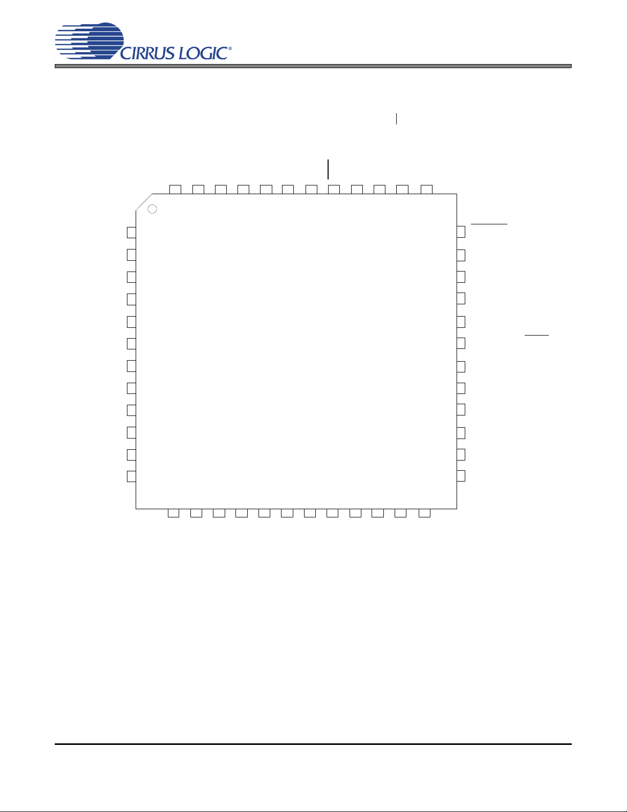
1. PIN DESCRIPTION
AIN3+
SDOUT1/TDM
VLS
SDOUT4
SDOUT3/TDM
GND
SDOUT2
M0/SDA/CDOUT
AIN5-
AIN1+
AIN5+
AIN6-
AIN6+
AIN3-
AIN7+
AIN7-
AIN8-
XTI
XTO
MCLK
AIN8+
VLC
DIF0/AD0/CS
DIF1/AD1/CDIN
AIN1-
M1/SCL/CCLK
VX
SCLK
LRCK/FS
OVFL
GND
MDIV
RST
6
2
4
8
10
1
3
5
7
9
11
12
13 14 15 16 17 18 19 20 21 22 23 24
31
35
33
29
27
36
34
32
30
28
26
25
48 47 46 45 44 43 42 41 40 39 38 37
CS5368
FILT+
AIN2-
VA
GND
GND
AIN2+
GND
REF_GND
VA
AIN4+
AIN4-
VQ
GND
VD
CLKMODE
CS5368
Figure 1. CS5368 Pinout
6 DS624F5
Page 7
Pin Name Pin # Pin Description
AIN2+, AIN2AIN4+, AIN4AIN3+, AIN3AIN7+, AIN7AIN8+, AIN8AIN6+, AIN6AIN5+, AIN5AIN1+, AIN1-
GND
VA 4, 9 Analog Power (Input) - Positive power supply for the analog section
REF_GND 5
FILT+ 6 Positive Voltage Reference (Output) - Reference voltage for internal sampling circuits.
VQ 7 Quiescent Voltage (Output) - Filter connection for the internal quiescent reference voltage.
VX 20
XTI
XTO
MCLK 23
LRCK/FS 24
SCLK 25
SDOUT4 26 Serial Audio Data (Output) - Channels 7,8.
SDOUT2 27 Serial Audio Data (
VLS 28 Serial Audio Interface Power (Input) - Positive power for the serial audio interface.
SDOUT1/TDM 30 Serial Audio Data (Output) - Channels 1,2.
SDOUT3/TDM
VD 33 Digital Power (Input) - Positive power supply for the digital section.
VLC 35 Control Port Interface Power(Input) - Positive power for the control port interface.
OVFL
RST
1,2
11,12
13,14
15,16
17,18
43,44
45,46
47,48
10,19
29,32
Differential Analog (Inputs) - Audio signals are presented differently to the delta sigma modula-
tors via the AIN+/- pins.
3,8
Ground (Input) - Ground reference. Must be connected to analog ground.
Reference Ground (Input) - For the internal sampling circuits. Must be connected to analog
ground.
Crystal Oscillator Power (Input) - Also powers control logic to enable or disable oscillator cir-
cuits.
2122Crystal Oscillator Connections (Input/Output) - I/O pins for an external crystal which may be
used to generate MCLK.
System Master Clock (Input/Output) - When a crystal is used, this pin acts as a buffered MCLK
Source (Output). When the oscillator function is not used, this pin acts as an input for the system
master clock. In this case, the XTI and XTO pins must be tied low.
Serial Audio Channel Clock (Input/Output)
In I²S Mode, Serial Audio Channel Select. When low, the odd channels are selected.
In LJ Mode, Serial Audio Channel Select. When high, the odd channels are selected.
In TDM Mode, a frame sync signal. When high, it marks the beginning of a new frame of serial
audio samples. In Slave Mode, this pin acts as an input pin.
Main timing clock for the Serial Audio Interface (Input/Output) - During Master Mode, this pin
acts as an output, and during Slave Mode it acts as an input pin.
Output) - Channels 3,4.
31 Serial Audio Data (Output) - Channels 5,6. TDM is complementary TDM data.
36 Overflow (Output, open drain) - Detects an overflow condition on both left and right channels.
41 Reset (Input) - The device enters a low power mode when low.
Stand-Alone Mode
CLKMODE 34
DIF1
DIF0
M1
M0
MDIV 42
CLKMODE (Input) - Setting this pin HIGH places a divide-by-1.5 circuit in the MCLK path to the
core device circuitry.
37
DIF1, DIF0 (Input) - Inputs of the audio interface format.
38
39
Mode Selection (Input) - Determines the operational mode of the device.
40
MCLK Divider (Input) - Setting this pin HIGH places a divide-by-2 circuit in the MCLK path to the
core device circuitry.
CS5368
DS624F5 7
Page 8
Control Port Mode
CLKMODE 34
AD1/CDIN 37
AD0/CS
SCL/CCLK 39
SDA/CDOUT 40
MDIV 42
CLKMODE (Input) - This pin is ignored in Control Port Mode and the same functionality is
obtained from the corresponding bit in the Global Control Register. Note: Should be connected
to GND when using the part in Control Port Mode.
I²C Format, AD1 (Input) - Forms the device address input AD[1].
SPI Format, CDIN (Input) - Becomes the input data pin.
I²C Format, AD0 (Input) - Forms the device address input AD[0].
38
SPI Format, CS
I²C Format, SCL (Input) – Serial clock for the serial control port. An external pull-up resistor is
required for I²C control port operation.
SPI Format, CCLK (Input) – Serial clock for the serial control port.
I²C Format SDA (Input/Output) - Acts as an input/output data pin. An external pull-up resistor is
required for I²C control port operation.
SPI Format CDOUT (Output) - Acts as an output only data pin.
MCLK Divider (Input) - This pin is ignored in Control Port Mode and the same functionality is
obtained from the corresponding bit in the Global Control Register.
Note: Should be connected to GND when using the part in Control Port Mode.
(Input) - Acts as the active low chip select input.
CS5368
8 DS624F5
Page 9
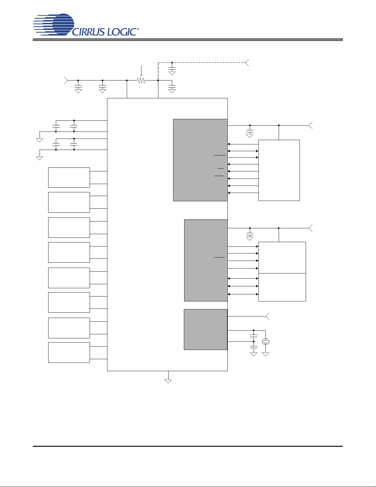
2. TYPICAL CONNECTION DIAGRAM
FILT+
D
+
VA V
+5V
5.1
1 F
+
SDOUT2
DIF0/AD0/CS
Power Down
and Mode
Settings
0.01
F
MODE0/SDA/CDOUT
MODE1/SCL/CCLK
REF_GND
VLC
F
AIN
+1
AIN
-
1
Channel 1 Analog
Input Buffer
AIN +2
AIN
-
2
Channel 2 Analog
Input Buffer
AIN +3
AIN
-
3
Channel 3 Analog
Input Buffer
AIN +4
AIN
-
4
Channel 4 Analog
Input Buffer
AIN
+5
AIN
-
5
Channel 5 Analog
Input Buffer
AIN
+6
AIN
-
6
Channel 6 Analog
Input Buffer
AIN
+7
AIN
-
7
Channel 7 Analog
Input Buffer
AIN
+8
AIN
-
8
Channel 8 Analog
Input Buffer
0.1 F
VQ
GND
220
F
0.1 F
+
1
F
GND
DIF1/AD1/CDIN
RST
OVFL
0.01
0.01F
+5V to 3.3V
1 F
+
A/D CONVERTER
CS5368
SDOUT1/ TDM
SDOUT4
SCLK
MCLK
Timing Logic
and Clock
Audio Data
Processor
MDIV
CLKMODE
39
40
36
37
38
41
42
34
27
31
30
26
24
25
23
LRCK/FS
+5V to 1.8V
6
5
7
8
47
48
1
2
13
14
11
12
45
46
43
44
15
16
17
18
3, 8, 10,
19, 29, 32
334, 9
35
VLS
F
0.01
28
XTI
XTO
21
22
+5V to 1.8V
+5V
VX
20
SDOUT3/ TDM
Resistor may only be used if
VD is derived from VA. If used,
do not drive any other logic
from VD.
CS5368
For analog buffer configurations, refer to Cirrus Application Note AN241. Also, a low-cost single-ended-to-differential solution is provided on the Customer Evaluation Board.
DS624F5 9
Figure 2. Typical Connection Diagram
Page 10
CS5368
3. CHARACTERISTICS AND SPECIFICATIONS
RECOMMENDED OPERATING CONDITIONS
GND = 0 V, all voltages with respect to 0 V.
Parameter Symbol Min Typ Max Unit
DC Power Supplies: Positive Analog
Positive Crystal
Positive Digital
Positive Serial Logic
Positive Control Logic
Ambient Operating Temperature (-CQZ)
(-DQZ)
VA
VX
VD
VLS
VLC
T
AC
T
AA
4.75
4.75
3.14
1.71
1.71
-40
-40
1
5.0
5.0
3.3
3.3
3.3
5.25 V
-
-
85
105
°C
1. TDM Quad-Speed Mode specified to operate correctly at VLS 3.14 V.
ABSOLUTE RATINGS
Operation beyond these limits may result in permanent damage to the device. Normal operation is not guaranteed
at these extremes. Transient currents up to ±100 mA on the analog input pins will not cause SCR latch-up.
Parameter Symbol Min Typ Max Units
DC Power Supplies: Positive Analog
Positive Crystal
Positive Digital
Positive Serial Logic
Positive Control Logic
Input Current I
Analog Input Voltage V
Digital Input Voltage V
Ambient Operating Temperature (Power Applied) T
Storage Temperature T
VA
VX
VD
VLS
VLC
in
IN
IND
A
stg
-0.3 - +6.0 V
-10
-0.3
-50 +125
-65 +150
-
10 mA
VA+ 0.3
VL+0.3
C
V
SYSTEM CLOCKING
Parameter Symbol Min Typ Max Unit
Input Master Clock Frequency MCLK 0.512 55.05 MHz
Input Master Clock Duty Cycle t
clkhl
10 DS624F5
40 60 %
Page 11
DC POWER
MCLK = 12.288 MHz; Master Mode; GND = 0 V.
Parameter Symbol Min Typ Max Unit
Power Supply Current VA = 5 V
(Normal Operation) VX = 5 V
VD = 5 V
VD = 3.3 V
VLS, VLC = 5 V
VLS, VLC = 3.3 V
Power Supply Current VA = VX = 5 V
(Power-Down) (Note 1) VLS, VLC, VD = 5 V
Power Consumption
Normal Operation All Supplies = 5 V
VA = VX = 5 V, VD = VLS = VLC = 3.3 V
(Power-Down) (Note 1)
I
A
I
X
I
D
I
D
I
L
I
L
I
A
I
D+L
--
-
-
100
4
70
42
12
5
50
500
930
675
2.75
CS5368
112
8
88
50
15
8
- A
1115
792
-
mA
mW
1. Power-Down is defined as RST
= LOW with all clocks and data lines held static at a valid logic level.
LOGIC LEVELS
Parameter Symbol Min Typ Max Units
High-Level Input Voltage %VLS/VLC V
Low-Level Input Voltage %VLS/VLC V
High-Level Output Voltage at 100 A load %VLS/VLC V
Low-Level Output Voltage at -100 A load %VLS/VLC V
SDA Low-Level Output Voltage at -2 mA load %VLC V
Current Sink
OVFL
Input Leakage Current logic pins only I
IH
IL
OH
OL
OL
in
70 - - %
--30%
85 - - %
--15%
--TBD%
-4 mA
-10 - 10 A
PSRR, VQ AND FILT+ CHARACTERISTICS
MCLK = 12.288 MHz; Master Mode. Valid with the recommended capacitor values on FILT+ and VQ as shown in
the “Typical Connection Diagram”.
Parameter Symbol Min Typ Max Unit
Power Supply Rejection Ratio at (1 kHz) PSRR - 65 - dB
V
Nominal Voltage
Q
Output Impedance
Maximum allowable DC current source/sink
Filt+ Nominal Voltage
Output Impedance
Maximum allowable DC current source/sink
-
-
VA/ 2
25
10
VA
4.4
10
V
-
-
k
A
V
k
A
DS624F5 11
Page 12
CS5368
ANALOG CHARACTERISTICS (COMMERCIAL)
Test Conditions (unless otherwise specified). VA = 5 V, VD = VLS = VLC 3.3 V, and TA = 25° C. Full-scale input
sine wave. Measurement Bandwidth is 10 Hz to 20 kHz.
Parameter Symbol Min Typ Max Unit
Single-Speed Mode Fs = 48 kHz
Dynamic Range A-weighted
unweighted
Total Harmonic Distortion + Noise -1 dB
referred to typical full scale -20 dB
-60 dB
Double-Speed Mode Fs = 96 kHz
Dynamic Range A-weighted
unweighted
40 kHz bandwidth unweighted
Total Harmonic Distortion + Noise -1 dB
referred to typical full scale -20 dB
-60 dB
40 kHz bandwidth -1dB
Quad-Speed Mode Fs = 192 kHz
Dynamic Range A-weighted
unweighted
40 kHz bandwidth unweighted
Total Harmonic Distortion + Noise -1 dB
referred to typical full scale -20 dB
-60 dB
40 kHz bandwidth -1dB
THD+N -
THD+N -
THD+N -
Dynamic Performance for All Modes
Interchannel Isolation - 110 - dB
DC Accuracy
Interchannel Gain Mismatch - 0.1 - dB
Gain Error -5 - 5 %
Gain Drift -
Offset Error HPF enabled
HPF disabled
Analog Input Characteristics
Full-scale Differential Input Voltage 1.07*VA 1.13*VA 1.19*VA Vpp
Input Impedance (Differential) - 250 - k
Common Mode Rejection Ratio CMRR - 82 - dB
108
105
108
105
-
108
105
-
0
-
114
111
-105
-91
-51
114
111
108
-105
-91
-51
-102
114
111
108
-105
-91
-51
-102
-
-
-99
-
-45
-dB
-99
-
-45
-
-dB
-99
-
-45
-
dB
dB
dB
dB
100 - ppm/°C
-
-
-
100
LSB
12 DS624F5
Page 13

CS5368
ANALOG CHARACTERISTICS (AUTOMOTIVE)
Test Conditions (unless otherwise specified). VA = 5.25 to 4.75 V, VD = 5.25 to 3.14 V, VLS = VLC = 5.25 to 1.71 V
and T
Single-Speed Mode Fs = 48 kHz
Dynamic Range A-weighted
Total Harmonic Distortion + Noise -1 dB
referred to typical full scale -20 dB
Double-Speed Mode Fs = 96 kHz
Dynamic Range A-weighted
Total Harmonic Distortion + Noise -1 dB
referred to typical full scale -20 dB
Quad-Speed Mode Fs = 192 kHz
Dynamic Range A-weighted
Total Harmonic Distortion + Noise -1 dB
referred to typical full scale -20 dB
Dynamic Performance for All Modes
Interchannel Isolation - 110 - dB
DC Accuracy
Interchannel Gain Mismatch - 0.1 - dB
Gain Error -7 - 7 %
Gain Drift -
Offset Error HPF enabled
Analog Input Characteristics
Full-scale Input Voltage 1.02*VA 1.13*VA 1.24*VA Vpp
Input Impedance (Differential) 250 - k
Common Mode Rejection Ratio CMRR - 82 - dB
= -40° to +85° C. Full-scale input sine wave. Measurement Bandwidth is 10 Hz to 20 kHz.
A
Parameter Symbol Min Typ Max Unit
unweighted
-60 dB
unweighted
40 kHz bandwidth unweighted
-60 dB
40 kHz bandwidth -1 dB
unweighted
40 kHz bandwidth unweighted
-60 dB
40 kHz bandwidth -1 dB
106
103
THD+N -
106
103
-
THD+N -
106
103
-
THD+N -
114
111
-105
-91
-51
114
111
108
-105
-91
-51
-102
114
111
108
-105
-91
-51
-102
100 - ppm/°C
HPF disabled
0
-
-
-
-dB
-97
-
-45
-dB
-97
-
-45
-
-dB
-97
-
-45
-
-
100
dB
dB
dB
LSB
DS624F5 13
Page 14

CS5368
DIGITAL FILTER CHARACTERISTICS
Parameter Symbol Min Typ Max Unit
Single-Speed Mode (2 kHz to 54 kHz sample rates)
Passband (Note 1) (-0.1 dB) 0
Passband Ripple -0.035 0.035 dB
Stopband (Note 1) 0.58
Stopband Attenuation -95 dB
Total Group Delay (Fs = Output Sample Rate) t
gd
-12/Fs s
-
Double-Speed Mode (54 kHz to 108 kHz sample rates)
Passband (Note 1) (-0.1 dB) 0
Passband Ripple -0.035 0.035 dB
Stopband (Note 1) 0.68
Stopband Attenuation -92 dB
Total Group Delay (Fs = Output Sample Rate) t
gd
-9/Fs s
-
Quad-Speed Mode (108 kHz to 216 kHz sample rates)
Passband (Note 1) (-0.1 dB) 0
Passband Ripple -0.035 0.035 dB
Stopband (Note 1) 0.78
Stopband Attenuation -92 dB
Total Group Delay (Fs = Output Sample Rate) t
gd
-5/Fs s
-
High-Pass Filter Characteristics
Frequency Response (Note 2) -3.0 dB
-0.13 dB
Phase Deviation
Passband Ripple -0dB
Filter Settling Time 10
(Note 2) @ 20 Hz
-
-
1
20
10 - Deg
5
/Fs - s
0.47 Fs
Fs
-
0.45 Fs
Fs
-
0.24 Fs
Fs
-
-Hz
Notes:
1. The filter frequency response scales precisely with Fs.
2. Response shown is for Fs equal to 48 kHz. Filter characteristics scale with Fs.
OVERFLOW TIMEOUT
Logic "0" = GND = 0 V; Logic "1" = VLS; CL = 30 pF, timing threshold is 50% of VLS.
Parameter Symbol Min Typ Max Unit
17
-1)/Fs
OVFL time-out on overrange condition
Fs = 44.1 kHz
Fs = 192 kHz
-
14 DS624F5
(2
2972
683
-ms
Page 15

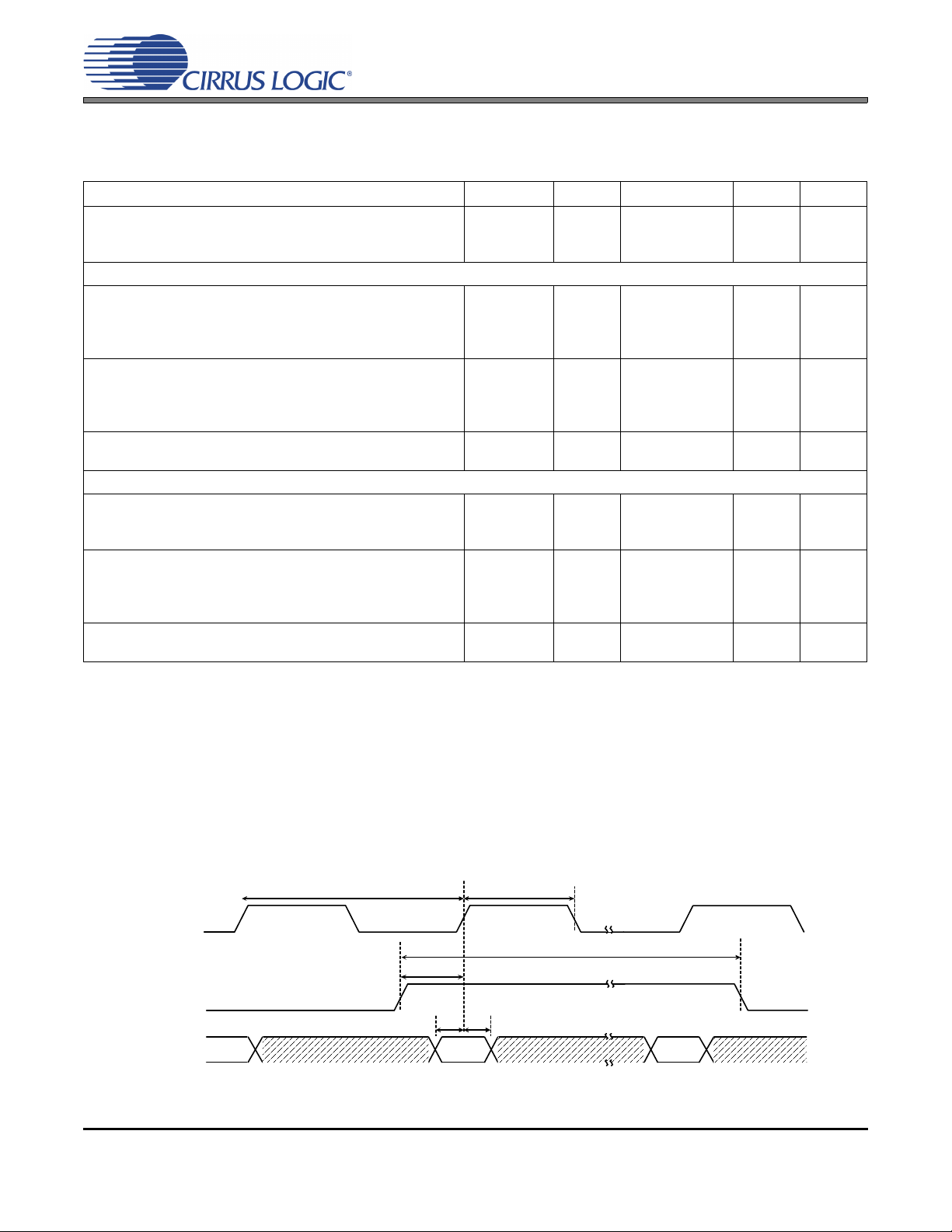
SERIAL AUDIO INTERFACE - I²S/LJ TIMING
LRCK
SDOUT
SCLK
data
channelchannel
data
t
HOLD2
t
SETUP2
t
HOLD1
t
SETUP1
t
PERIOD
t
HIGH
The serial audio port is a three-pin interface consisting of SCLK, LRCK and SDOUT.
Logic "0" = GND = 0 V; Logic "1" = VLS; C
Parameter Symbol Min Typ Max Unit
Sample Rates Single-Speed Mode
Double-Speed Mode
Master Mode
SCLK Frequency
SCLK Period 1/(64*216 kHz)
SCLK Duty Cycle (Note 1) (CLKMODE = 0)(Note 2)
(CLKMODE = 1)(Note 2)
LRCK setup before SCLK rising
LRCK hold after SCLK rising
SDOUT setup before SCLK rising
SDOUT hold after SCLK rising (VLS = 1.8 V)
after SCLK rising (VLS = 3.3 V)
after SCLK rising (VLS = 5 V)
Slave Mode
SCLK Frequency (Note 3)
SCLK Period 1/(64*216 kHz)
SCLK Duty Cycle
LRCK setup before SCLK rising
LRCK hold after SCLK rising
SDOUT setup before SCLK rising (VLS = 1.8 V)
before SCLK rising (VLS = 3.3 V)
before SCLK rising (VLS = 5 V)
SDOUT hold after SCLK rising (VLS = 1.8 V)
after SCLK rising (VLS = 3.3 V)
after SCLK rising (VLS = 5 V)
= 20 pF, timing threshold is 50% of VLS.
L
-
Quad-Speed Mode
-
t
PERIOD
t
HIGH
t
HIGH
t
SETUP1
t
HOLD1
t
SETUP2
t
HOLD2
t
HOLD2
t
HOLD2
64*Fs
72.3
-
t
PERIOD
t
HIGH
t
SETUP1
t
HOLD1
t
SETUP2
t
SETUP2
t
SETUP2
t
HOLD2
t
HOLD2
t
HOLD2
72.3
2
54
108
40
28
20
20
10
20
10
5
-
28
20
20
4
10
10
20
10
5
CS5368
54
-
-
50
33
--ns
--ns
64*Fs
-
-
--ns
--ns
108
216
64*Fs
60
38
-
65
kHz
Hz
ns
%
%
Hz
ns
%
Notes:
1. Duty cycle of generated SCLK depends on duty cycle of received MCLK as specified under “System
Clocking” on page 10.
2. CLKMODE functionality described in Section 4.6.3 "Master Mode Clock Dividers" on page 24.
3. In Slave Mode, the SCLK/LRCK ratio can be set according to preference. However, chip performance
is guaranteed only when using the ratios in Section 4.7 Master and Slave Clock Frequencies on page
25.
DS624F5 15
Figure 3. I²S/LJ Timing
Page 16
SERIAL AUDIO INTERFACE - TDM TIMING
FS
SDOUT
SCLK
data data
t
HOLD2
t
SETUP2
t
SETUP1
new frame
data
t
PERIOD
t
HIGH1
t
HIGH2
The serial audio port is a three-pin interface consisting of SCLK, LRCK and SDOUT.
Logic "0" = GND = 0 V; Logic "1" = VLS; C
Parameter Symbol Min Typ Max Unit
Sample Rates Single-Speed Mode
Double-Speed Mode
Master Mode
SCLK Frequency
SCLK Period 1/(256*216 kHz)
SCLK Duty Cycle (Note 2) (CLKMODE = 0)(Note 3)
(CLKMODE = 1)(Note 3)
FS setup before SCLK rising (Single-Speed Mode)
FS setup before SCLK rising (Double-Speed Mode)
FS setup before SCLK rising (Quad-Speed Mode)
FS width in SCLK cycles
SDOUT setup before SCLK rising
SDOUT hold after SCLK rising
Slave Mode
SCLK Frequency (Note 4)
SCLK Period 1/(256*216 kHz)
SCLK Duty Cycle
FS setup before SCLK rising (Single-Speed Mode)
FS setup before SCLK rising (Double-Speed Mode)
FS setup before SCLK rising (Quad-Speed Mode)
FS width in SCLK cycles
SDOUT setup before SCLK rising
SDOUT hold after SCLK rising
= 20 pF, timing threshold is 50% of VLS.
L
-
-
-
t
PERIOD
t
HIGH1
t
HIGH1
t
SETUP1
t
SETUP1
t
SETUP1
t
HIGH2
t
SETUP2
t
HOLD2
t
PERIOD
t
HIGH1
t
SETUP1
t
SETUP1
t
SETUP1
t
HIGH2
t
SETUP2
t
HOLD2
Quad-Speed Mode
1
2
54
108
256*Fs
18
40
28
20
18
5
128
5
5
18
28
20
20
10
1
5
5
-
-
-
-
50
33
-
-
-
-
-
-
256*Fs
-
-
-
-
-
-
-
-
54
108
216
256*Fs
60
38
-
-
-
128
-
-
-
65
-
-
-
244
-
-
CS5368
kHz
kHz
kHz
Hz
ns
%
%
ns
ns
ns
-
ns
ns
Hz
ns
%
ns
ns
ns
-
ns
ns
Notes:
1. TDM Quad-Speed Mode only specified to operate correctly at VLS 3.14 V.
2. Duty cycle of generated SCLK depends on duty cycle of received MCLK as specified under “System
Clocking” on page 10.
3. CLKMODE functionality described in Section 4.6.3 "Master Mode Clock Dividers" on page 24.
4. In Slave Mode, the SCLK/LRCK ratio can be set according to preference; chip performance is guaranteed only when using the ratios in Section 4.7 Master and Slave Clock Frequencies on page 25.
16 DS624F5
Figure 4. TDM Timing
Page 17

SWITCHING SPECIFICATIONS - CONTROL PORT - I²C TIMING
t
buf
t
hdst
t
lo wthdd
t
high
t
sud
Stop S ta rt
SDA
SCL
t
irs
RST
t
hdst
t
rc
t
fc
t
sust
t
susp
Start
Stop
Repe ated
t
rd
t
fd
t
ack
Inputs: Logic 0 = DGND, Logic 1 = VLC, SDA CL=30pF
Parameter Symbol Min Max Unit
SCL Clock Frequency f
Rising Edge to Start t
RST
Bus Free Time Between Transmissions t
Start Condition Hold Time (prior to first clock pulse) t
Clock Low time t
Clock High Time t
Setup Time for Repeated Start Condition t
SDA Hold Time from SCL Falling (Note 1)
SDA Setup time to SCL Rising (Note 2) t
Rise Time of SCL and SDA t
Fall Time SCL and SDA t
Setup Time for Stop Condition t
Acknowledge Delay from SCL Falling t
Notes:
scl
irs
buf
hdst
low
high
sust
t
hdd
sud
rc
fc
susp
ack
- 100 kHz
600
4.7 µs
4.0
4.7
4.0
4.7
0
600 ns
-1µs
-300ns
4.7 - µs
300 1000 ns
CS5368
ns
µs
1. Data must be held for sufficient time to bridge the transition time, t
, of SCL.
fc
Figure 5. I²C Timing
2. The operational timing specification deviates from the I2C-Bus Specification and User Manual of
250 ns.
DS624F5 17
Page 18

SWITCHING SPECIFICATIONS - CONTROL PORT - SPI TIMING
CS
CCLK
CDIN
CDOUT
RST
t
srs
t
scl
t
sch
t
css
t
r2
t
f2
t
csh
t
dsutdh
t
pd
Inputs: Logic 0 = DGND, Logic 1 = VLC, CDOUT CL=30pF
Parameter Symbol Min Max Units
CCLK Clock Frequency f
RST
Rising Edge to CS Falling t
CS
Falling to CCLK Edge t
CS High Time Between Transmissions t
CCLK Low Time t
CCLK High Time t
CDIN to CCLK Rising Setup Time t
CCLK Rising to DATA Hold Time (Note 1) t
CCLK Falling to CDOUT Stable t
Rise Time of CDOUT t
Fall Time of CDOUT t
Rise Time of CCLK and CDIN (Note 2) t
Fall Time of CCLK and CDIN (Note 2) t
sck
srs
css
csh
scl
sch
dsu
dh
pd
r1
f1
r2
f2
06.0MHz
20
20
1.0 s
66
66
40
15
-
100
50
25
CS5368
ns
-
ns
Notes:
1. Data must be held for sufficient time to bridge the transition time of CCLK.
2. For f
<1 MHz
sck
Figure 6. SPI Timing
18 DS624F5
Page 19

4. APPLICATIONS
4.1 Power
CS5368 features five independent power pins that power various functional blocks within the device and
allow for convenient interfacing to other devices. Table 1 shows what portion of the device is powered from
each supply pin. Please refer to “Recommended Operating Conditions” on page 10 for the valid range of
each power supply pin. The power supplied to each power pin can be independent of the power supplied to
any other pin.
To meet full performance specifications, the CS5368 requires normal low-noise board layout. The “Typical
Connection Diagram” on page 9 shows the recommended power arrangements, with the VA pins connected
to a clean supply. VD, which powers the digital filter, may be run from the system logic supply, or it may be
powered from the analog supply via a single-pole decoupling filter.
CS5368
Power Supply Pin
Pin Name Pin Number Functional Block
VA 4, 9 Analog Core
VX 20 Crystal Oscillator
VD 33 Digital Core
VLS 28 Serial Audio Interface
VLC 35 Control Logic
Table 1. Power Supply Pin Definitions
Decoupling capacitors should be placed as near to the ADC as possible, with the lower value high-frequency capacitors placed nearest to the device leads. Clocks should be kept away from the FILT+ and VQ pins
in order to avoid unwanted coupling of these signals into the device. The FILT+ and VQ decoupling capacitors must be positioned to minimize the electrical path to ground.
The CDB5368 evaluation board demonstrates optimum layout for the device.
4.2 Control Port Mode and Stand-Alone Operation
4.2.1 Stand-Alone Mode
In Stand-Alone Mode, the CS5368 is programmed exclusively with multi-use configuration pins. This mode
provides a set of commonly used features, which comprise a subset of the complete set of device features
offered in Control Port Mode.
To use the CS5368 in Stand-Alone Mode, the configuration pins must be held in a stable state, at valid logic
levels, and RST
tion on the reset function is available in Section 4.5 on page 22.
must be asserted until the power supplies and clocks are stable and valid. More informa-
4.2.2 Control Port Mode
In Control Port Mode, all features of the CS5368 are available. Four multi-use configuration pins become
software pins that support the I²C or SPI bus protocol. To initiate Control Port Mode, a controller that supports I²C or SPI must be used to enable the internal register functionality. This is done by setting the CPEN bit (Bit 7 of the Global Control Port Register). Once CP-EN is set, all of the device configuration pins
are ignored, and the internal register settings determine the operating modes of the part. Figure 4.13 on
page 30 provides detailed information about the I²C and SPI bus protocols.
DS624F5 19
Page 20

4.3 Master Clock Source
XTI
XTO
22
21
The CS5368 requires a Master Clock that can come from one of two sources: an on-chip crystal oscillator
driver or an externally generated clock.
4.3.1 On-Chip Crystal Oscillator Driver
When using the on-board crystal oscillator driver, the XTI pin (pin 21) is the input for the Master Clock (MCLK) to the device. The XTO pin (pin 22) must not be used to drive anything other than the oscillator tank
circuitry. When using the on-board crystal driver, the topology shown in Figure 7 must be used. The crystal
oscillator manufacturer supplies recommended capacitor values. A buffered copy of the XTI input is available as an output on the MCLK pin (pin 23), which is level-controlled by VLS and may be used to synchronize other parts to the device.
CS5368
Figure 7. Crystal Oscillator Topology
4.3.2 Externally Generated Master Clock
If an external clock is used, the XTI and XTO pins must be grounded, and the MCLK pin becomes an input
for the system master clock. The incoming MCLK should be at the logic level set by the user on the VLS
supply pin.
20 DS624F5
Page 21

4.4 Master and Slave Operation
ADC as
clock
master
Controller
LRCK/FS
SCLK
ADC as
clock
slave
Controller
LRCK/FS
SCLK
Master
ADC
Slave1
ADC
Slave2
ADC
Slave3
ADC
SCLK & LRCK/FS
CS5368 operation depends on two clocks that are synchronously derived from MCLK: SCLK and LRCK/FS.
See Section 4.5 on page 22 for a detailed description of SCLK and LRCK/FS.
The CS5368 can operate as either clock master or clock slave with respect to SCLK and LRCK/FS. In Master Mode, the CS5368 derives SCLK and LRCK/FS synchronously from MCLK and outputs the derived
clocks on the SCLK pin (pin 25) and the LRCK/FS pin (pin 24), respectively. In Slave Mode, the SCLK and
LRCK/FS are inputs, and the input signals must be synchronously derived from MCLK by a separate device
such as another CS5368 or a microcontroller. Figure 8 illustrates the clock flow of SCLK and LRCK/FS in
both Master and Slave Modes.
The Master/Slave operation is controlled through the settings of M1 and M0 pins in Stand-Alone Mode or
by the M[1] and M[0] bits in the Global Mode Control Register in Control Port Mode. See Section 4.6 on page
23 for more information regarding the configuration of M1 and M0 pins or M[1] and M[0] bits.
Figure 8. Master/Slave Clock Flow
CS5368
4.4.1 Synchronization of Multiple Devices
To ensure synchronous sampling in applications where multiple ADCs are used, the MCLK and LRCK must
be the same for all CS5368 devices in the system. If only one master clock source is needed, one solution
is to place one CS5368 in Master Mode, and slave all of the other devices to the one master, as illustrated
in Figure 9. If multiple master clock sources are needed, one solution is to supply all clocks from the same
external source and time the CS5368 reset de-assertion with the falling edge of MCLK. This will ensure that
all converters begin sampling on the same clock edge.
Figure 9. Master and Slave Clocking for a Multi-Channel Application
DS624F5 21
Page 22

4.5 Serial Audio Interface (SAI) Format
Odd Channels 1,3, ...
Even Channels 2,4, ...
LRCK
receiver latches data on rising edges of SCLK
SDOUT
SCLK
MSB
...
LSB MSB
...
LSB MSB
Odd Channels 1,3, ...
Even Channels 2,4, ...
LRCK
receiver latches data on rising edges of SCLK
MSB
...
LSB MSBMSB
...
LSBSDOUT
SCLK
The SAI port consists of two timing pins (SCLK, LRCK/FS) and four audio data output pins (SDOUT1/TDM,
SDOUT2, SDOUT3/TDM
and SDOUT4). The CS5368 output is serial data in I²S, Left-Justified (LJ), or Time
Division Multiplexed (TDM) digital audio interface formats. These formats are available to the user in both
Stand-Alone Mode and Control Port Mode.
4.5.1 I²S and LJ Format
The I²S and LJ formats are both two-channel protocols. During one LRCK period, two channels of data are
transmitted, odd channels first, then even. The MSB is always clocked out first.
In Slave Mode, the number of SCLK cycles per channel is fixed as described under “Serial Audio Interface
- I²S/LJ Timing” on page 15. In Slave Mode, if more than 32 SCLK cycles per channel are received from a
master controller, the CS5368 will fill the longer frame with trailing zeros. If fewer than 24 SCLK cycles per
channel are received from a master, the CS5368 will truncate the serial data output to the number of SCLK
cycles received. For a complete overview of serial audio interface formats, please refer to Cirrus Logic Application Note AN282.
CS5368
Figure 10. I²S Format
Figure 11. LJ Format
22 DS624F5
Page 23

4.5.2 TDM Format
Channel 6
SCLK
MSB LSBMSB LSBMSB LSBMSB LSBMSB LS BMSB
TDM O UT
Channel 1 Channel 4Channel 2 C hannel 5Channel 3
32 clks 32 clks 32 clks 32 clks 32 clks 32 clks
Channel 8
LSBMSB LS BMSB
Channel 7
32 clks 32 clks
FS
MSB
LSB
LSB
LSBMSB
Data
Zeroes
In TDM Mode, all eight channels of audio data are serially clocked out during a single Frame Sync (FS)
cycle, as shown in Figure 12. The rising edge of FS signifies the start of a new TDM frame cycle. Each
channel slot occupies 32 SCLK cycles, with the data left justified and with MSB first. TDM output data
should be latched on the rising edge of SCLK within time specified under ”Serial Audio Interface - TDM Tim-
ing” section on page 16. The TDM data output port resides on the SDOUT1 pin. The TDM
complimentary TDM data. All SDOUT pins will remain active during TDM Mode. Refer to Section 4.11 “Op-
timizing Performance in TDM Mode” on page 29 for critical system design information.
Figure 12. TDM Format
4.5.3 Configuring Serial Audio Interface Format
The serial audio interface format of the data is controlled by the configuration of the DIF1 and DIF0 pins in
Stand-Alone Mode or by the DIF[1] and DIF[0] bits in the Global Mode Control Register in Control Port
Mode, as shown in Table 2.
CS5368
output pin is
DIF1 DIF0 Mode
0 0 Left-Justified
01 I²S
10 TDM
11 Reserved
Table 2. DIF1 and DIF0 Pin Settings
4.6 Speed Modes
4.6.1 Sample Rate Ranges
CS5368 supports sampling rates from 2 kHz to 21 kHz, divided into three ranges: 2 kHz - 54 kHz, 54 kHz 108 kHz, and 108 kHz - 216 kHz. These sampling speed modes are called Single-Speed Mode (SSM),
Double-Speed Mode (DSM), and Quad-Speed Mode (QSM), respectively.
4.6.2 Using M1 and M0 to Set Sampling Parameters
The Master/Slave operation and the sample rate range are controlled through the settings of the M1 and
M0 pins in Stand-Alone Mode, or by the M[1] and M[0] bits in the Global Mode Control Register in Control
Port Mode, as shown in Table 3.
M1 M0 Mode Frequency Range
0 0 Single-Speed Master Mode (SSM) 2 kHz - 54 kHz
0 1 Double-Speed Master Mode (DSM) 54 kHz - 108 kHz
1 0 Quadruple-Speed Master Mode (QSM) 108 kHz - 216 kHz
1 1 Auto-Detected Speed Slave Mode 2 kHz - 216 kHz
Table 3. M1 and M0 Settings
DS624F5 23
Page 24

4.6.3 Master Mode Clock Dividers
÷ 128
÷ 64
M0M1
LRCK/ FS
Single
Speed
Quad
Speed
Double
Speed
00
01
10
÷ 2
÷ 4
÷ 1
SCLK
Single
Speed
Quad
Speed
Double
Speed
00
01
10
÷ 256
pin
CLKMODE
MDIV
n/a
MCLK
÷ 1
÷ 1.5 ÷ 2
÷ 1
÷ 2
÷ 1
bit MDIV1
MDIV0
0/1 0/1 0/1
MCLK DIVIDERS
SAMPLE RATE DIVIDERS
CLKMODE
128
64
Single-Speed
256
pin
CLKMODE
MDIV
n/a
External
MCLK
÷ 1
÷ 1.5 ÷ 2
÷ 1
÷ 2
÷ 1
bit MDIV1
MDIV0
0/1 0/1 0/1
MCLK DIVIDERS
CLKMODE
÷LRCK
LRCK
Double-Speed
Quad-Speed
SPEED MODE
Internal
MCLK
Figure 13 shows the configuration of the MCLK dividers and the sample rate dividers for Master Mode, in-
cluding the significance of each MCLK divider pin (in Stand-Alone Mode) or bit (in Control Port Mode).
CS5368
4.6.4 Slave Mode Audio Clocking With Auto-Detect
24 DS624F5
Figure 13. Master Mode Clock Dividers
In Slave Mode, CS5368 auto-detects speed mode, which eliminates the need to configure M1 and M0 when
changing among speed modes. The external MCLK is subject to clock dividers as set by the clock divider
pins in Stand-Alone Mode or the clock divider bits in Control Port Mode. The CS5368 compares the divideddown, internal MCLK to the incoming LRCK/FS and sets the speed mode based on the MCLK/LRCK ratio
as shown in Figure 14.
Figure 14. Slave Mode Auto-Detect Speed
Page 25
CS5368
4.7 Master and Slave Clock Frequencies
Tables 4 through 12 show the clock speeds for sample rates of 48 kHz, 96 kHz and 192 kHz. The MC-
LK/LRCK ratio should be kept at a constant value during each mode. In Master Mode, the device outputs
the frequencies shown. In Slave Mode, the SCLK/LRCK ratio can be set according to design preference.
However, device performance is guaranteed only when using the ratios shown in the tables.
Control Port Mode only
LJ/I²S MASTER OR SLAVE SSM Fs = 48 kHz
MCLK Divider 4 3 2 1.5 1
MCLK (MHz)
SCLK (MHz)
MCLK/LRCK Ratio 1024 768 512 384 256
SCLK/LRCK Ratio
Table 4. Frequencies for 48 kHz Sample Rate using LJ/I²S
LJ/I²S MASTER OR SLAVE DSM Fs = 96 kHz
MCLK Divider 4 3 2 1.5 1
MCLK (MHz) 49.152 36.864 24.567 18.384 12.288
SCLK (MHz)
MCLK/LRCK Ratio
SCLK/LRCK Ratio 64 64 64 64 64
Table 5. Frequencies for 96 kHz Sample Rate using LJ/I²S
49.152 36.864 24.576 18.384 12.288
3.072 3.072 3.072 3.072 3.072
64 64 64 64 64
6.144 6.144 6.144 6.144 6.144
512 384 256 192 128
LJ/I²S MASTER OR SLAVE QSM Fs = 192 kHz
MCLK Divider 4 3 2 1.5 1
MCLK (MHz) 49.152 36.864 24 18.384 12.288
SCLK (MHz)
MCLK/LRCK Ratio
SCLK/LRCK Ratio 64 64 64 64 64
Table 6. Frequencies for 192 kHz Sample Rate using LJ/I²S
12.288 12.288 12.288 12.288 12.288
256 192 128 96 64
TDM MASTER SSM Fs = 48 kHz
MCLK Divider 4 3 2 1.5 1
MCLK (MHz) 49.152 36.864 24.567 18.384 12.288
SCLK (MHz)
MCLK/FS Ratio
SCLK/FS Ratio 256 256 256 256 256
Table 7. Frequencies for 48 kHz Sample Rate using TDM
12.288 12.288 12.288 12.288 12.288
1024 768 512 384 256
TDM SLAVE SSM Fs = 48 kHz
MCLK Divider 4 3 2 1.5 1
MCLK (MHz)
SCLK (MHz)
MCLK/FS Ratio 1024 768 512 384 256
SCLK/FS Ratio
Table 8. Frequencies for 48 kHz Sample Rate using TDM
49.152 36.864 24.567 18.384 12.288
12.288 12.288 12.288 12.288 12.288
256 256 256 256 256
DS624F5 25
Page 26

CS5368
TDM MASTER DSM Fs = 96 kHz
MCLK Divider 4 3 2- -
MCLK (MHz)
SCLK (MHz)
MCLK/FS Ratio
SCLK/FS Ratio
Table 9. Frequencies for 96 kHz Sample Rate using TDM
TDM SLAVE DSM Fs = 96 kHz
MCLK Divider 4 3 2 1.5 1
MCLK (MHz)
SCLK (MHz) 24.576 24.576 24.576 24.576 24.576
MCLK/FS Ratio
SCLK/FS Ratio
Table 10. Frequencies for 96 kHz Sample Rate using TDM
TDM MASTER QSM Fs = 192 kHz
MCLK Divider 4 ----
MCLK (MHz)
SCLK (MHz) 49.152 - - - -
MCLK/FS Ratio
SCLK/FS Ratio
Table 11. Frequencies for 192 kHz Sample Rate using TDM
49.152 36.864 24.567 - -
24.576 24.576 24.576 - -
512 384 256 - -
256 256 256 - -
49.152 36.864 24.567 18.384 12.288
512 384 256 192 128
256 256 256 256 256
49.152 - - - -
256 - - - -
256 - - - -
TDM SLAVE QSM Fs = 192 kHz
MCLK Divider 4 3 2 1.5 1
MCLK (MHz)
SCLK (MHz) 49.152 49.152 49.152 49.152 49.152
MCLK/FS Ratio
SCLK/FS Ratio
Table 12. Frequencies for 192 kHz Sample Rate using TDM
49.152 36.864 24.567 18.384 12.288
256 192 128 96 64
256 256 256 256 256
26 DS624F5
Page 27

4.8 Reset
The device should be held in reset until power is applied and all incoming clocks are stable and valid. Upon
de-assertion of RST
starts sending audio output data a maximum of 524288 MCLK cycles after the release of RST
ing between mode configurations in Stand-Alone Mode, including clock dividers, serial audio interface format, master/slave, or speed modes, it is recommended to reset the device following the change by holding
the RST
pin low for a minimum of one MCLK cycle and then restoring the pin to a logic-high condition.
, the state of the configuration pins is latched, the state machine begins, and the device
4.8.1 Power-Down Mode
The CS5368 features a Power-Down Mode in which power is temporarily withheld from the modulators, the
crystal oscillator driver, the digital core, and the serial port. The user can access Power-Down Mode by
holding the device in reset and holding all clock lines at a static, valid logic level (either logic-high or logiclow). “DC Power” on page 11 shows the power-saving associated with Power-Down Mode.
4.9 Overflow Detection
4.9.1 Overflow in Stand-Alone Mode
The CS5368 includes overflow detection on all input channels. In Stand-Alone Mode, this information is
presented as open drain, active low on the OVFL
range condition in any channel is detected. The data will remain low, then time-out as specified in Section
"Overflow Timeout" on page 14. After the time-out, the OVFL
been any other over-range condition detected. Note that an over-range condition on any channel will restart
the time-out period.
CS5368
. When chang-
pin. The pin will go to a logical low as soon as an over-
pin will return to a logical high if there has not
4.9.2 Overflow in Control Port Mode
In Control Port Mode, the Overflow Status Register interacts with the Overflow Mask Register to provide
interrupt capability for each individual channel. See Section 5.4 "02h (OVFL) Overflow Status Register" on
page 33 for details on these two registers.
DS624F5 27
Page 28

4.10 Analog Connections
VQ
+
634
634
91
91
+
-
-
2700 pF
470 pF
470 pF
COG
COG
10 uF
10 uF
ADC AIN+
ADC AIN-
AIN+
AIN-
COG
100
k
10 k
10
k
100
k
The analog modulator samples the input at half of the internal Master Clock frequency, or 6.144 MHz nominally. The digital filter will reject signals within the stopband of the filter. However, there is no rejection of
input signals that are at (N X 6.144 MHz) the digital passband frequency, where n=0,1,2.... Refer to
Figure 15, which shows the suggested filter that will attenuate any noise energy at 6.144 MHz in addition to
providing the optimum source impedance for the modulators. The use of capacitors that have a large voltage coefficient (such as general-purpose ceramics) must be avoided since these can degrade signal linearity. COG capacitors are recommended for this application. For additional configurations, refer to Cirrus
Application Note AN241.
CS5368
Figure 15. Recommended Analog Input Buffer
28 DS624F5
Page 29

4.11 Optimizing Performance in TDM Mode
Noise Management is a design technique that is utilized in the majority of audio A/D converters. Noise management is relatively simple conceptually. The goal of noise management is to interleave the on-chip digital
activity with the analog sampling processes to ensure that the noise generated by the digital activity is minimized (ideally non-existant) when the analog sampling occurs. Noise management, when implemented
properly, minimizes the on-chip interference between the analog and digital sections of the device. This
technique has proven to be very effective and has simplified the process of implementing an A/D converter
into a systems design. The dominate source of interference (and most difficult to control) is the activity on
the serial audio interface (SAI). However, noise management becomes more difficult to implement as audio
sample rates increase simply due to the fact that there is less time between transitions on the SAI.
The CS5368 A/D converter supports a multi-channel Time-Division-Multiplexed interface for Single, Double
and Quad-Speed sampling modes. In Single-Speed Mode, sample rates below 50 kHz, the required frequencies of the audio serial ports are sufficiently low that it is possible to implement noise-management. In
this mode, the performance of the devices are relatively immune to activity on the audio ports.
However, in Double-Speed and Quad-Speed modes there is insufficient time to implement noise management due to the required frequencies of the audio ports. Therefore, analog performance, both dynamic
range and THD+N, can be degraded if the serial port transitions occurr concurrently with the analog sampling. The magnitude of the interference is not only related to the timing of the transition but also the di/dt or
transient currents associated with the activity on the serial ports. Even though there is insufficient time to
properly implement noise management, the interference effects can be minimized by controlling the transient currents required of the serial ports in Double- and Quad-Speed TDM Modes.
CS5368
In addition to standard mixed-signal design techniques, system performance can be maximized by following
several guidelines during design.
– Operate the serial audio port at 3.3 V and not 5 V. The lower serial port voltage lowers transent
currents.
– Operate the A/D converter as a system clock Slave. The serial clock and Left/Right clock become high-
impedence inputs in this mode and do not generate significant transient currents.
– Place a buffer on the serial data output very near the A/D converter. Minimizing the stray capacitance
of the printed circuit board trace and the loading presented by other devices on the serial data line will
minimize the transient current.
– Place a resistor, near the converter, beween the A/D serial data output and the buffer. This resistor will
reduce the instantaneous switching currents into the capacitive loads on the nets, resulting in a slower
edge rate. The value of the resistor should be as high as possible without causing timing problems
elsewhere in the system.
4.12 DC Offset Control
The CS5368 includes a dedicated high-pass filter for each channel to remove input DC offset at the system
level. A DC level may result in audible “clicks” when switching between devices in a multi-channel system.
In Stand-Alone Mode, all of the high-pass filters remain enabled. In Control Port Mode, the high-pass filters
default to enabled, but may be controlled by writing to the HPF
spective high-pass filter is enabled, and it continuously subtracts a measure of the DC offset from the output
of the decimation filter. If any HPF
ister is frozen, and this DC offset will continue to be subtracted from the conversion result.
register. If any HPF bit is taken low, the re-
bit is taken high during device operation, the value of the DC offset reg-
DS624F5 29
Page 30

4.13 Control Port Operation
MAP
MSB
LSB
DATA
byte 1
byte n
R/W
R/W
ADDRESS
CHIP
ADDRESS
CHIP
CDIN
CCLK
CS
CDOUT
MSB
LSB
MSB
LSB
1001111
1001111
MAP = Memory Address Pointer, 8 bits, MSB first
High Impedance
The Control Port is used to read and write the internal device registers. It supports two industry standard
formats, I²C and SPI. The part is in I²C format by default. SPI Mode is selected if there is ever a high-to-low
transition on the AD0/CS
pin after the RST pin has been restored high.
In Control Port Mode, all features of the CS5368 are available. Four multi-use configuration pins become
software pins that support the I²C or SPI bus protocol. To initiate Control Port Mode, a controller that supports I²C or SPI must be used to enable the internal register functionality. This is done by setting the
CP-EN bit (Bit 7 of the Global Control Port Register). Once CP-EN is set, all of the device configuration pins
are ignored, and the internal register settings determine the operating modes of the part.
4.13.1 SPI Mode
In SPI Mode, CS is the CS5368 chip select signal; CCLK is the control port bit clock (input into the CS5368
from a controller); CDIN is the input data line from a controller; CDOUT is the output data line to a controller.
Data is clocked in on the rising edge of CCLK and is supplied on the falling edge of CCLK.
To write to a register, bring CS low. The first seven bits on CDIN form the chip address and must be
1001111. The eighth bit is a read/write indicator (R/W), which should be low to write. The next eight bits
form the Memory Address Pointer (MAP), which is set to the address of the register that is to be updated.
The next eight bits are the data that will be placed into the register designated by the MAP. During writes,
the CDOUT output stays in the Hi-Z state. It may be externally pulled high or low with a 47 k resistor, if
desired.
CS5368
There is a MAP auto-increment capability, which is enabled by the INCR bit in the MAP register. If INCR is
a zero, the MAP will stay constant for successive read or writes. If INCR is set to a 1, the MAP will autoincrement after each byte is read or written, allowing block reads or writes of successive registers.
To read a register, the MAP has to be set to the correct address by executing a partial write cycle that finishes (CS
desired. To begin a read, bring CS
high) immediately after the MAP byte. The MAP auto-increment bit (INCR) may be set or not, as
low, send out the chip address and set the read/write bit (R/W) high.
The next falling edge of CCLK will clock out the MSB of the addressed register (CDOUT will leave the high
impedance state). If the MAP auto-increment bit is set to 1, the data for successive registers will appear
consecutively
.
Figure 16. SPI Format
30 DS624F5
Page 31

4.13.2 I²C Mode
4 5 6 7 24 25
SCL
CHIP ADDRESS (WRITE) MAP BYTE DATA
DATA +1
START
ACK
STOP
ACKACKACK
1 0 0 1 1 AD1 AD0 0
SDA
INCR 6 5 4 3 2 1 0 7 6 1 0 7 6 1 0 7 6 1 0
0 1 2 3 8 9 12 16 17 18 1910 11 13 14 15 27 28
26
DATA +n
SCL
CHIP ADDRESS ( WRITE)
MAP BYTE
DATA
DATA +1
START
ACK
STOP
ACK
ACK
ACK
1 0 0 1 1 AD1 AD0 0
SDA
1 0 0 1 1 AD1 AD0 1
CHIP ADDRESS ( READ)
START
INCR 6 5 4 3 2 1 0
7 0 7 0 7 0
NO
168 9 12 13 14 154 5 6 7 0 1 20 21 22 23 24
26 27 28
2 3 10 11 17 18 19 25
ACK
DATA + n
STOP
In I²C Mode, SDA is a bidirectional data line. Data is clocked into and out of the part by the clock, SCL.
There is no CS pin. Pins AD0 and AD1 form the two least-significant bits of the chip address and should
be connected through a resistor to VLC or DGND, as desired. The state of the pins is latched when the
CS5368 is being released from RST.
A Start condition is defined as a falling transition of SDA while SCL is high. A Stop condition is a rising transition of SDA while SCL is high. All other transitions of SDA occur while SCL is low. The first byte sent to
the CS5368 after a Start condition consists of a 7-bit chip address field and a R/W bit (high for a read, low
for a write). The upper five bits of the 7-bit address field are fixed at 10011. To communicate with a CS5368,
the chip address field, which is the first byte sent to the CS5368, should match 10011 and be followed by
the settings of the AD1 and AD0. The eighth bit of the address is the R/W bit. If the operation is a write, the
next byte is the Memory Address Pointer (MAP), which selects the register to be read or written. If the operation is a read, the contents of the register pointed to by the MAP will be output. Setting the auto-increment bit in MAP allows successive reads or writes of consecutive registers. Each byte is separated by an
acknowledge bit. The ACK bit is output from the CS5368 after each input byte is read and is input to the
CS5368 from the microcontroller after each transmitted byte.
Since the read operation cannot set the MAP, an aborted write operation is used as a preamble. The write
operation is aborted after the acknowledge for the MAP byte by sending a Stop condition. The following
pseudocode illustrates an aborted write operation followed by a read operation.
Send start condition.
Send 10011xx0 (chip address & write operation).
Receive acknowledge bit.
Send MAP byte, auto increment off.
Receive acknowledge bit.
Send stop condition, aborting write.
Send start condition.
Send 10011xx1 (chip address & read operation).
Receive acknowledge bit.
Receive byte, contents of selected register.
Send acknowledge bit.
Send stop condition.
CS5368
Figure 17. I²C Write Format
DS624F5 31
Figure 18. I²C Read Format
Page 32

CS5368
5. REGISTER MAP
In Control Port Mode, the bits in these registers are used to control all of the programmable features of the ADC. All
registers above 0Ah are RESERVED.
5.1 Register Quick Reference
Adr Name7654 3210
00 REVI CHIP-ID[3:0] REVISION[3:0]
01 GCTL CP-EN CLKMODE MDIV[1:0] DIF[1:0] MODE[1:0]
02 OVFL OVFL8 OVFL7 OVFL6 OVFL5 OVFL4 OVFL3 OVFL2 OVFL1
03 OVFM OVFM8 OVFM7 OVFM6 OVFM5 OVFM4 OVFM3 OVFM2 OVFM1
04 HPF HPF8 HPF7 HPF6 HPF5 HPF4 HPF3 HPF2 HPF1
05 RESERVED - - - - - - - -
06 PDNE RESERVED PDN-BG PDN-OSC PDN87 PDN65 PDN43 PDN21
07 RESERVED - - - - - - - -
08 MUTE MUTE8 MUTE7 MUTE6 MUTE5 MUTE4 MUTE3 MUTE2 MUTE1
09 RESERVED - - - - - - - -
0A SDEN RESERVED SDEN4
SDEN3 SDEN2 SDEN1
5.2 00h (REVI) Chip ID Code & Revision Register
R/W76543210
R CHIP-ID[3:0] REVISION[3:0]
Default: See description
The Chip ID Code & Revision Register is used to store the ID and revision of the chip.
Bits[7:4] contain the chip ID, where the CS5368 is represented with a value of 0x8.
Bits[3:0] contain the revision of the chip, where revision A is represented as 0x0, revision B is represented
as 0x1, etc.
5.3 01h (GCTL) Global Mode Control Register
R/W76543210
R/W CP-EN CLKMODE MDIV[1:0] DIF[1:0] MODE[1:0]
Default: 0x00
The Global Mode Control Register is used to control the Master/Slave Speed modes, the serial audio data
format and the Master clock dividers for all channels. It also contains a Control Port enable bit.
Bit[7] CP-EN manages the Control Port Mode. Until this bit is asserted, all pins behave as if in Stand-Alone
Mode. When this bit is asserted, all pins used in Stand-Alone Mode are ignored, and the corresponding register values become functional.
Bit[6] CLKMODE Setting this bit puts the part in 384X mode (divides XTI by 1.5), and clearing the bit invokes 256X mode (divide XTI by 1.0 - pass through).
32 DS624F5
Page 33

CS5368
Bits[5:4] MDIV[1:0] Each bit selects an XTI divider. When either bit is low, an XTI divide-by-1 function is
selected. When either bit is HIGH, an XTI divide-by-2 function is selected. With both bits HIGH, XTI is divided by 4.
The table below shows the composite XTI division using both CLKMODE and MDIV[1:0].
CLKMODE,MDIV[1],MDIV[0] DESCRIPTION
000 Divide-by-1
100 Divide-by-1.5
001 or 010 Divide-by-2
101 or 110 Divide-by-3
011 Divide-by-4
111 Reser ved
Bits[3:2] DIF[1:0] Determine which data format the serial audio interface is using to clock-out data.
DIF[1:0]
0x00 Left-Justified format
0x01 I²S format
0x02 TDM
0x03 Reserved
Bits[1:0] MODE[1:0] This bit field determines the device sample rate range and whether it is operating as
an audio clocking Master or Slave.
MODE[1:0]
0x00 Single-Speed Mode Master
0x01 Double-Speed Mode Master
0x02 Quad-Speed Mode Master
0x03 Slave Mode all speeds
5.4 02h (OVFL) Overflow Status Register
R/W76543210
ROVFL8
OVFL7 OVFL6 OVFL5 OVFL4 OVFL3 OVFL2 OVFL1
Default: 0xFF, no overflows have occurred.
Note: This register interacts with Register 03h, the Overflow Mask Register.
The Overflow Status Register is used to indicate an individual overflow in a channel. If an overflow condition
on any channel is detected, the corresponding bit in this register is asserted (low) in addition to the open
drain active low OVFL
pin going low. Each overflow status bit is sticky and is cleared only when read, pro-
viding full interrupt capability.
5.5 03h (OVFM) Overflow Mask Register
R/W76543210
R/W OVFM8 OVFM7 OVFM6 OVFM5 OVFM4 OVFM3 OVFM2 OVFM1
Default: 0xFF, all overflow interrupts enabled.
The Overflow Mask Register is used to allow or prevent individual channel overflow events from creating
activity on the OVFL
bit in the Overflow Status register is prevented from causing any activity on the OVFL
pin. When a particular bit is set low in the Mask register, the corresponding overflow
pin.
DS624F5 33
Page 34

CS5368
5.6 04h (HPF) High-Pass Filter Register
R/W76543210
R/W HPF8
Default: 0x00, all high-pass filters enabled.
The High-Pass Filter Register is used to enable or disable a high-pass filter that exists for each channel.
These filters are used to perform DC offset calibration, a procedure that is detailed in “DC Offset Control”
on page 29.
5.7 05h Reserved
R/W76543210
RESERVED - - - - - - - -
5.8 06h (PDN) Power Down Register
R/W76543210
R/W RESERVED PDN-BG PDN-OSC PDN87 PDN65 PDN43 PDN21
Default: 0x00 - everything powered up
The Power Down Register is used as needed to reduce the chip’s power consumption.
Bit[7] RESERVED
HPF7 HPF6 HPF5 HPF4 HPF3 HPF2 HPF1
Bit[6] RESERVED
Bit[5] PDN-BG When set, this bit powers-down the bandgap reference.
Bit[4] PDN-OSC controls power to the internal oscillator core. When asserted, the internal oscillator core is
shut down, and no clock is supplied to the chip. If the chip is running off an externally supplied clock at the
MCLK pin, it is also prevented from clocking the device internally.
Bit[3:0] PDN When any bit is set, all clocks going to a channel pair are turned off, and the serial data outputs
are forced to all zeroes.
5.9 07h Reserved
R/W76543210
RESERVED - - - - - - - -
5.10 08h (MUTE) Mute Control Register
R/W76543210
R/W MUTE8 MUTE7 MUTE6 MUTE5 MUTE4 MUTE3 MUTE2 MUTE1
Default: 0x00, no channels are muted.
The Mute Control Register is used to mute or unmute the serial audio data output of individual channels.
When a bit is set, that channel’s serial data is muted by forcing the output to all zeroes.
34 DS624F5
Page 35

CS5368
5.11 09h Reserved
R/W76543210
RESERVED - - - - - - - -
5.12 0Ah (SDEN) SDOUT Enable Control Register
R/W76543210
R/W RESERVED SDEN4 SDEN3 SDEN2 SDEN1
Default: 0x00, all SDOUT pins enabled.
The SDOUT Enable Control Register is used to tri-state the serial audio data output pins. Each bit, when
set, tri-states the associated SDOUT pin.
DS624F5 35
Page 36

6. FILTER PLOTS
0 0.05 0.1 0.15 0.2 0.25 0.3 0.35 0.4 0.45 0.
5
−0.1
−0.08
−0.06
−0.04
−0.02
0
0.02
0.04
0.06
0.08
0.1
Frequency (normalized to Fs)
Amplitude (dB)
0 0.05 0.1 0.15 0.2 0.25 0.3 0.35 0.4 0.45 0.
5
−0.1
−0.08
−0.06
−0.04
−0.02
0
0.02
0.04
0.06
0.08
0.1
Frequency (normalized to Fs)
Amplitude (dB)
0 0.05 0.1 0.15 0.2 0.2
5
−0.1
−0.08
−0.06
−0.04
−0.02
0
0.02
0.04
0.06
0.08
0.1
Frequency (normalized to Fs)
Amplitude (dB)
CS5368
Figure 19. SSM Passband
Figure 20. DSM Passband
36 DS624F5
Figure 21. QSM Passband
Page 37

Figure 22. SSM Stopband
0 0.1 0.2 0.3 0.4 0.5 0.6 0.7 0.8 0.9
−140
−120
−100
−80
−60
−40
−20
0
Frequency (normalized to Fs)
Amplitude (dB)
0 0.1 0.2 0.3 0.4 0.5 0.6 0.7 0.8 0.9
−140
−120
−100
−80
−60
−40
−20
0
Frequency (normalized to Fs)
Amplitude (dB)
0 0.1 0.2 0.3 0.4 0.5 0.6 0.7 0.8 0.9
−120
−100
−80
−60
−40
−20
0
Frequency (normalized to Fs)
Amplitude (dB)
CS5368
1
DS624F5 37
1
Figure 23. DSM Stopband
1
Figure 24. QSM Stopband
Page 38

Figure 25. SSM -1 dB Cutoff
0.4 0.42 0.44 0.46 0.48 0.5 0.52 0.54 0.56 0.58 0.
6
−2
−1.8
−1.6
−1.4
−1.2
−1
−0.8
−0.6
−0.4
−0.2
0
Frequency (normalized to Fs)
Amplitude (dB)
0.4 0.42 0.44 0.46 0.48 0.5 0.52 0.54 0.56 0.58 0.
6
−2
−1.8
−1.6
−1.4
−1.2
−1
−0.8
−0.6
−0.4
−0.2
0
Frequency (normalized to Fs)
Amplitude (dB)
0.2 0.22 0.24 0.26 0.28 0.3 0.32 0.34 0.36 0.38 0.
4
−2
−1.8
−1.6
−1.4
−1.2
−1
−0.8
−0.6
−0.4
−0.2
0
Frequency (normalized to Fs)
Amplitude (dB)
CS5368
Figure 26. DSM -1 dB Cutoff
38 DS624F5
Figure 27. QSM -1 dB Cutoff
Page 39

7. PARAMETER DEFINITIONS
Dynamic Range
The ratio of the rms value of the signal to the rms sum of all other spectral components over the specified
bandwidth. Dynamic Range is a signal-to-noise ratio measurement over the specified bandwidth made with
a -60 dBFS signal. 60 dB is added to resulting measurement to refer the measurement to full scale. This
technique ensures that the distortion components are below the noise level and do not affect the measurement. This measurement technique has been accepted by the Audio Engineering Society, AES17-199, and
the Electronic Industries Association of Japan, EIAJ CP-307. Expressed in decibels. The dynamic range is
specified with and without an A-weighting filter.
Total Harmonic Distortion + Noise
The ratio of the rms value of the signal to the rms sum of all other spectral components over the specified
bandwidth (typically 10 Hz to 20 kHz), including distortion components. Expressed in decibels. Measured
at -1 and -20 dBFS as suggested in AES17-1991 Annex A. Specified using an A-weighting filter.
Frequency Response
A measure of the amplitude response variation from 10 Hz to 20 kHz relative to the amplitude response at
1 kHz. Units in decibels.
Interchannel Isolation
A measure of crosstalk between one channel and all remaining channels, measured for each channel at the
converter's output with no signal to the input under test and a full-scale signal applied to all other channels.
Units in decibels.
CS5368
Interchannel Gain Mismatch
The gain difference between left and right channels. Units in decibels.
Gain Error
The deviation from the nominal full-scale analog output for a full-scale digital input.
Gain Drift
The change in gain value with temperature. Units in ppm/°C.
Offset Error
The deviation of the mid-scale transition (111...111 to 000...000) from the ideal. Units in mV.
Intrachannel Phase Deviation
The deviation from linear phase within a given channel.
Interchannel Phase Deviation
The difference in phase response between channels.
DS624F5 39
Page 40

8. PACKAGE DIMENSIONS
E1
E
D1
D
1
e
L
B
A1
A
48L LQFP PACKAGE DRAWING
E1
E
D1
D
1
e
L
B
A1
A
CS5368
DIM MIN NOM MAX MIN NOM MAX
A --- 0.055 0.063 --- 1.40 1.60
A1 0.002 0.004 0.006 0.05 0.10 0.15
B 0.007 0.009 0.011 0.17 0.22 0.27
D 0.343 0.354 0.366 8.70 9.0 BSC 9.30
D1 0.272 0.28 0.280 6.90 7.0 BSC 7.10
E 0.343 0.354 0.366 8.70 9.0 BSC 9.30
E1 0.272 0.28 0.280 6.90 7.0 BSC 7.10
e* 0.016 0.020 0.024 0.40 0.50 BSC 0.60
L 0.018 0.24 0.030 0.45 0.60 0.75
* Nominal pin pitch is 0.50 mm
Controlling dimension is mm. JEDEC Designation: MS026
0.000° 4° 7.000° 0.00° 4° 7.00°
INCHES MILLIMETERS
THERMAL CHARACTERISTICS
Parameter Symbol Min Typ Max Unit
Allowable Junction Temperature - - 135 C
Package Thermal Resistance
40 DS624F5
JA
JC
-48-
-15-
C/W
Page 41

CS5368
9. ORDERING INFORMATION
Product Description Package Pb-Free Grade Temp Range Container Order #
114dB, 192kHz,
CS5368
CDB5368 Evaluation Board for CS5368 CDB5368
8-channel A/D
Converter
48-pin
LQFP
YES
Commercial -40°C to +85°C
Automotive -40°C to +105°C
Tray CS5368-CQZ
Tape & Reel CS5368-CQZR
Tray CS5368-DQZ
Tape & Reel CS5368-DQZR
10.REVISION HISTORY
Revision Changes
F1
DEC ‘06
F2
JUL ‘07
F3
JAN ‘08
F4
APR ‘09
F5
JUL ‘14
Initial release.
Updated the wording of pin 24, LRCK/FS, in the pin description table on page 7 to correctly reflect the
high/low clocking state for odd-channel c in I²S and LJ Modes.
Corrected SCL/CCLK pin description (Pin 39) for "Control Port Mode" on page 8.
Corrected Absolute Max temp for “Ambient Operating Temperature (Power Applied)” on page 10.
Updated I
Added Note 2 to “Switching Specifications - Control Port - I²C Timing” on page 17.
2
C and SPI bullet under “Additional Control Port Features” on page 1.
DS624F5 41
Page 42

CS5368
Contacting Cirrus Logic Support
For all product questions and inquiries, contact a Cirrus Logic Sales Representative.
To find the one nearest you, go to www.cirrus.com.
IMPORTANT NOTICE
Cirrus Logic, Inc. and its subsidiaries ("Cirrus") believe that the information contained in this document is accurate and reliable. However, the information is subject
to change without notice and is provided "AS IS" without warranty of any kind (express or implied). Customers are advised to obtain the latest version of relevant
information to verify, before placing orders, that information being relied on is current and complete. All products are sold subject to the terms and conditions of sale
supplied at the time of order acknowledgment, including those pertaining to warranty, indemnification, and limitation of liability. No responsibility is assumed by Cirrus
for the use of this information, including use of this information as the basis for manufacture or sale of any items, or for infringement of patents or other rights of third
parties. This document is the property of Cirrus and by furnishing this information, Cirrus grants no license, express or implied under any patents, mask work rights,
copyrights, trademarks, trade secrets or other intellectual property rights. Cirrus owns the copyrights associated with the information contained herein and gives consent for copies to be made of the information only for use within your organization with respect to Cirrus integrated circuits or other products of Cirrus. This consent
does not extend to other copying such as copying for general distribution, advertising or promotional purposes, or for creating any work for resale.
CERTAIN APPLICATIONS USING SEMICONDUCTOR PRODUCTS MAY INVOLVE POTENTIAL RISKS OF DEATH, PERSONAL INJURY, OR SEVERE PROPERTY OR ENVIRONMENTAL DAMAGE (“CRITICAL APPLICATIONS”). CIRRUS PRODUCTS ARE NOT DESIGNED, AUTHORIZED OR WARRANTED FOR USE
IN PRODUCTS SURGICALLY IMPLANTED INTO THE BODY, AUTOMOTIVE SAFETY OR SECURITY DEVICES, LIFE SUPPORT PRODUCTS OR OTHER CRITICAL APPLICATIONS. INCLUSION OF CIRRUS PRODUCTS IN SUCH APPLICATIONS IS UNDERSTOOD TO BE FULLY AT THE CUSTOMER’S RISK AND
CIRRUS DISCLAIMS AND MAKES NO WARRANTY, EXPRESS, STATUTORY OR IMPLIED, INCLUDING THE IMPLIED WARRANTIES OF MERCHANTABILITY
AND FITNESS FOR PARTICULAR PURPOSE, WITH REGARD TO ANY CIRRUS PRODUCT THAT IS USED IN SUCH A MANNER. IF THE CUSTOMER OR
CUSTOMER’S CUSTOMER USES OR PERMITS THE USE OF CIRRUS PRODUCTS IN CRITICAL APPLICATIONS, CUSTOMER AGREES, BY SUCH USE, TO
FULLY INDEMNIFY CIRRUS, ITS OFFICERS, DIRECTORS, EMPLOYEES, DISTRIBUTORS AND OTHER AGENTS FROM ANY AND ALL LIABILITY, INCLUDING ATTORNEYS’ FEES AND COSTS, THAT MAY RESULT FROM OR ARISE IN CONNECTION WITH THESE USES.
Cirrus Logic, Cirrus, and the Cirrus Logic logo designs are trademarks of Cirrus Logic, Inc. All other brand and product names in this document may be trademarks
or service marks of their respective owners.
SPI is a trademark of Motorola, Inc.
42 DS624F5
 Loading...