

Page 1
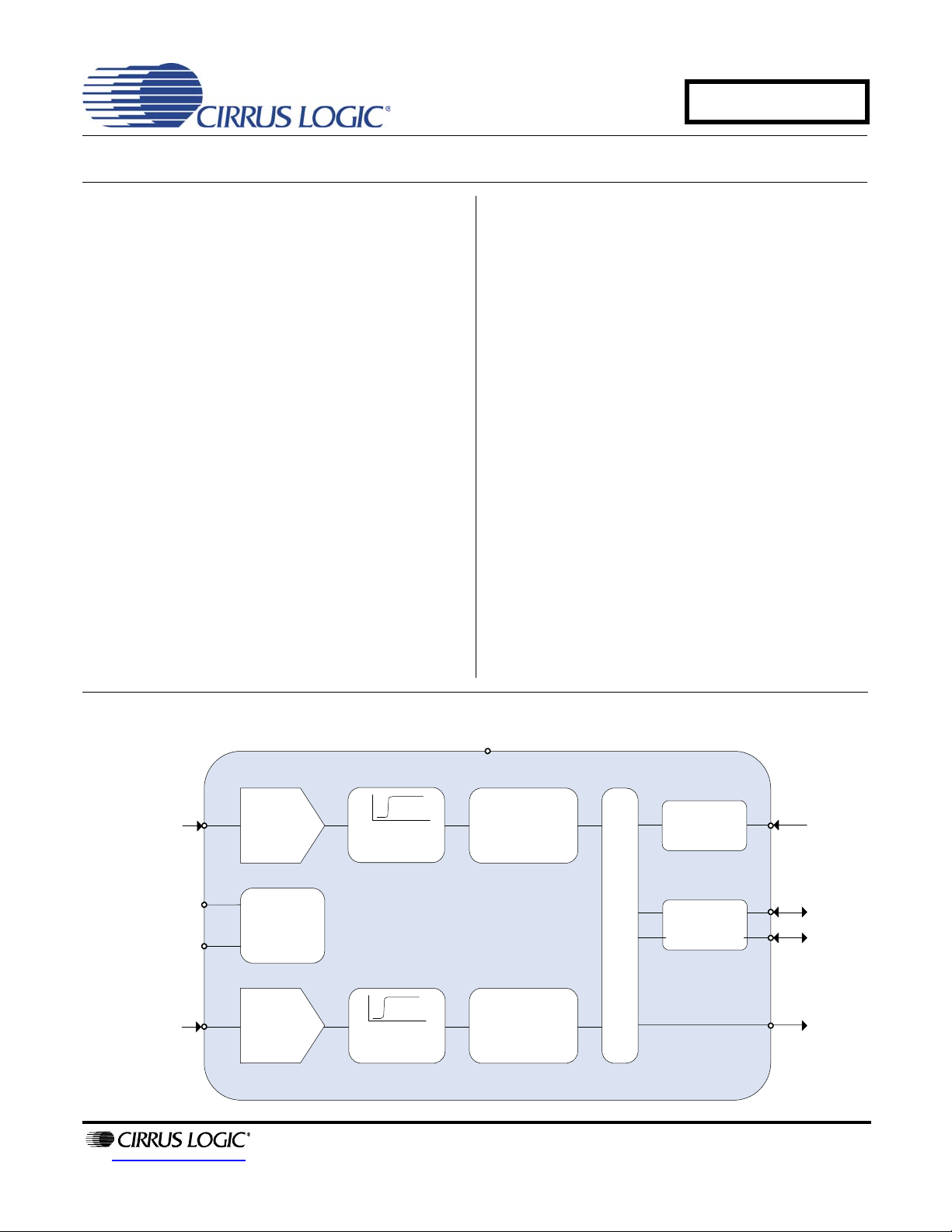
High-Pass
Filter
High-Pass
Filter
Low-Latency
Digital F ilters
VA
3.3 V to 5 V
Interna l
Reference
Voltages
High-Z
Sampling
Network
Auto-detect
MCLK Divider
Master
Clock
Single-Ended
Analog Input
Low-Latency
Digital F ilters
High-Z
Sampling
Network
Single-Ended
Analog Input
SCLK
LRCK
SDOUT
FILT+
VQ
AINR
AINL
Serial Port
Slave Mode
Auto-detect
High-Pass
Filter
Draft
2/1/11
CS5343/4
98 dB, 96 kHz, Multi-Bit Audio A/D Converter
Features
Advanced Multi-Bit Architecture
24-bit Conversion
Supports Audio Sample Rates Up to 108 kHz
98 dB Dynamic Range at 5 V
-92 dB THD+N at 5 V
Low-Latency Digital Filter
High-Pass Filter to Remove DC Offsets
Single +3.3 V or +5 V Power Supply
Power Consumption < 40 mW at 3.3 V
Master or Slave Operation
Slave Mode Speed Auto-Detect
Master Mode Default Settings
256x or 384x MCLK/LRCK Ratio
CS5343 Supports I²S Audio Format
CS5344 Supports Left-Justified Audio Format
General Description
The CS5343/4 is a complete analog-to-digital converter
for digital audio systems. It perfor ms sa mplin g, an alog to-digital conversion, and anti-alias filtering, generating
24-bit values for both left and right inputs in serial form
at sample rates up to 108 kHz per channel.
The CS5343/4 uses a 3rd-order, multi-bit Delta-Sigma
modulator followed by a digital filter, which removes the
need for an external anti-alias filter.
The CS5343/4 also features a high-impedance sampling network which eliminates costly external
components such as op-amps.
The CS5343/4 is available in a 10-pin TSSOP package
for both Commercial (-40° to +85° C) and Automotive
grades (-40° to +105° C). The CDB5343 Customer
Demonstration Board is also available for device evaluation and implementation suggestions. Please refer to
the “Ordering Information” on page 19 for complete
details.
The CS5343/4 is ideal for audio systems requiring wide
dynamic range, negligible distortion and low noise, such
as set-top boxes, DVD-karaoke players, DVD recorders, A/V receivers, and automotive applications.
http://www.cirrus.com
Copyright Cirrus Logic, Inc. 2011
(All Rights Reserved)
February '11
DS687F4
Page 2

TABLE OF CONTENTS
1. PIN DESCRIPTIONS .............................................................................................................................. 3
2. CHARACTERISTICS AND SPECIFICATIONS ...................................................................................... 4
RECOMMENDED OPERATING CONDITIONS ..................................................................................... 4
ABSOLUTE MAXIMUM RATINGS ......................................................................................................... 4
ANALOG CHARACTERISTICS - COMMERCIAL GRADE (-CZZ) ......................................................... 5
ANALOG CHARACTERISTICS - AUTOMOTIVE GRADE (-DZZ) ......................................................... 6
DIGITAL FILTER CHARACTERISTICS ................................................................................................7
DC ELECTRICAL CHARACTERISTICS ........................ ... ... .......................................... ... ... .... ... ........... 7
DIGITAL CHARACTERISTICS ............................................................................................................... 8
SYSTEM CLOCKING AND SERIAL AUDIO INTERFACE ..................................................................... 9
3. TYPICAL CONNECTION DIAGRAM ................................................................................................... 11
4. APPLICATIONS ................................................................................................................................... 12
4.1 Operation as Clock Master or Slave ............................................................................................... 12
4.1.1 Slave Mode Operation .................... .... ... ... ....................................... ... ... .... ... ... ... ... .... ............ 12
4.1.2 Master Mode Operation ......................................................................................................... 13
4.1.2.1 Master Mode Speed Selection ................................................................................... 13
4.1.3 Master Clock ............................................... .... ... ... ... .... ... ... ... ................................................ 13
4.2 Serial Audio Interface ..................................................................................................................... 14
4.3 Digital Interface ............................................................................................................................... 14
4.4 Analog Connections ....................................................................................................................... 14
4.4.1 Component Values ... .......................................... .......................................... ... ...................... 15
4.5 Grounding and Power Supply Decoupling ...................... ... .... ... ... ... ... .... .........................................15
4.6 Synchronization of Multiple Devices ............................................................................................... 16
5. FILTER PLOTS - ALL SPEED MODES ............................................................................................... 16
6. PARAMETER DEFINITIONS ................................................................................................................ 17
7. PACKAGE DIMENSIONS .................................................................................................................... 18
THERMAL CHARACTERISTICS .......................................................................................................... 18
8. ORDERING INFORMATION ................................................................................................................ 19
9. REVISION HISTORY ............................................................................................................................ 20
Draft
2/1/11
CS5343/4
2 DS687F4
Page 3
Draft
1
2
3
4
5
6
7
8
9
10
SDOUT
SCLK
LRCK
MCLK
FILT+
VA
GND
AINR
VQ
AINL
2/1/11
CS5343/4
1. PIN DESCRIPTIONS
Pin Name Pin # Pin Description
SDOUT 1
SCLK 2 Serial Clock (Input/Output) - Serial clock for the serial audio interface.
LRCK 3
MCLK 4 Master Clock (Input) - Clock source for the delta-sigma modulator and digital filters.
FILT+ 5 Positive Voltage Reference (Output) - Positive reference voltage for the internal sampling circuits.
AINL
AINR
VQ 7 Quiescent Voltage (Output) - Filter connection for the internal quiescent reference voltage.
GND 9 Ground (Input) - Ground reference. Must be connected to analog ground.
VA 10 Power (Input) - Positive power supply for the digital and analog sections.
Serial Audio Data Output (Output) - Output for two’s complement serial audio data. Also selects Master
or Slave Mode; See Section 4.1 on page 12 for details.
Left Right Clock (Input/Output) - Determines which channel, Left or Right, is currently active on the
serial audio data line.
68Analog Input (Input) - The full-scale analog input level is specified in the Analog Characteristics specifi-
cation table.
DS687F4 3
Page 4
Draft
2/1/11
CS5343/4
2. CHARACTERISTICS AND SPECIFICATIONS
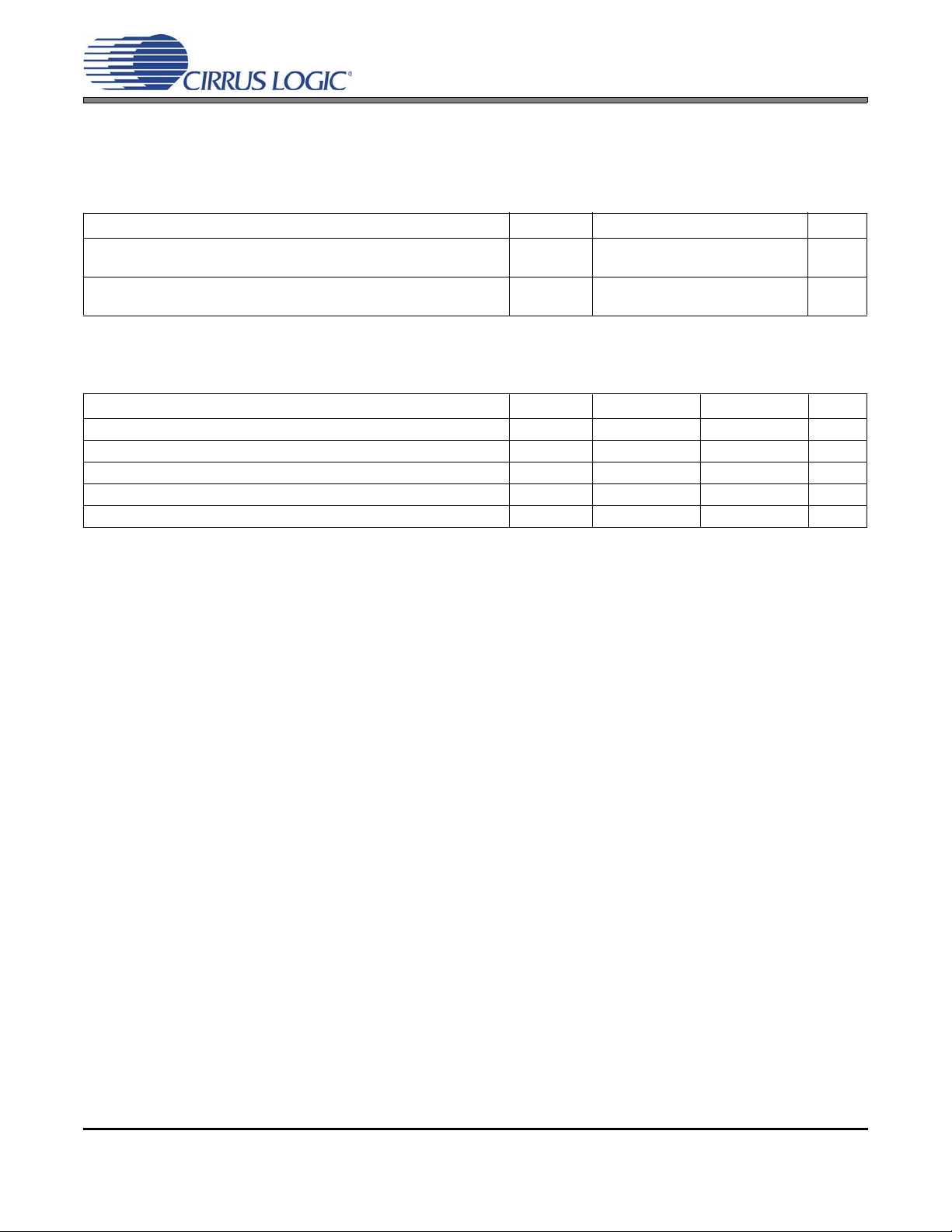
RECOMMENDED OPERATING CONDITIONS
GND = 0 V, all voltages with respect to GND.
Parameter Symbol Min Typ Max Unit
Power Supplies
Ambient Operating Temperature Commercial (-CZZ)
Automotive (-DZZ)
T
T
VA
AC
AD
3.1
4.75
-40
-40
3.3
5.0
3.5
5.25
-
-
85
105
ABSOLUTE MAXIMUM RATINGS
GND = 0 V, all voltages with respect to GND. (Note 1)
Parameter Symbol Min Max Unit
DC Power Supplies VA -0.3 +6.0 V
Input Current (Note 2) I
Input Voltage (Note 3) V
Ambient Operating Temperature (Power Applied) T
Storage Temperature T
in
IN
A
stg
-10 10 mA
-0.7 VA+0.7 V
-50 +115 C
-65 +150 C
V
V
°C
°C
Notes:
1. Operation beyond these limits may result in permanent damage to the device. Normal operation is not
guaranteed at these extremes.
2. Any pin except supplies. Transient currents of up to ±100 mA on the analog input pins will not cause
SCR latch-up.
3. The maximum over/under voltage is limited by the input current.
4 DS687F4
Page 5
Draft
2/1/11
CS5343/4
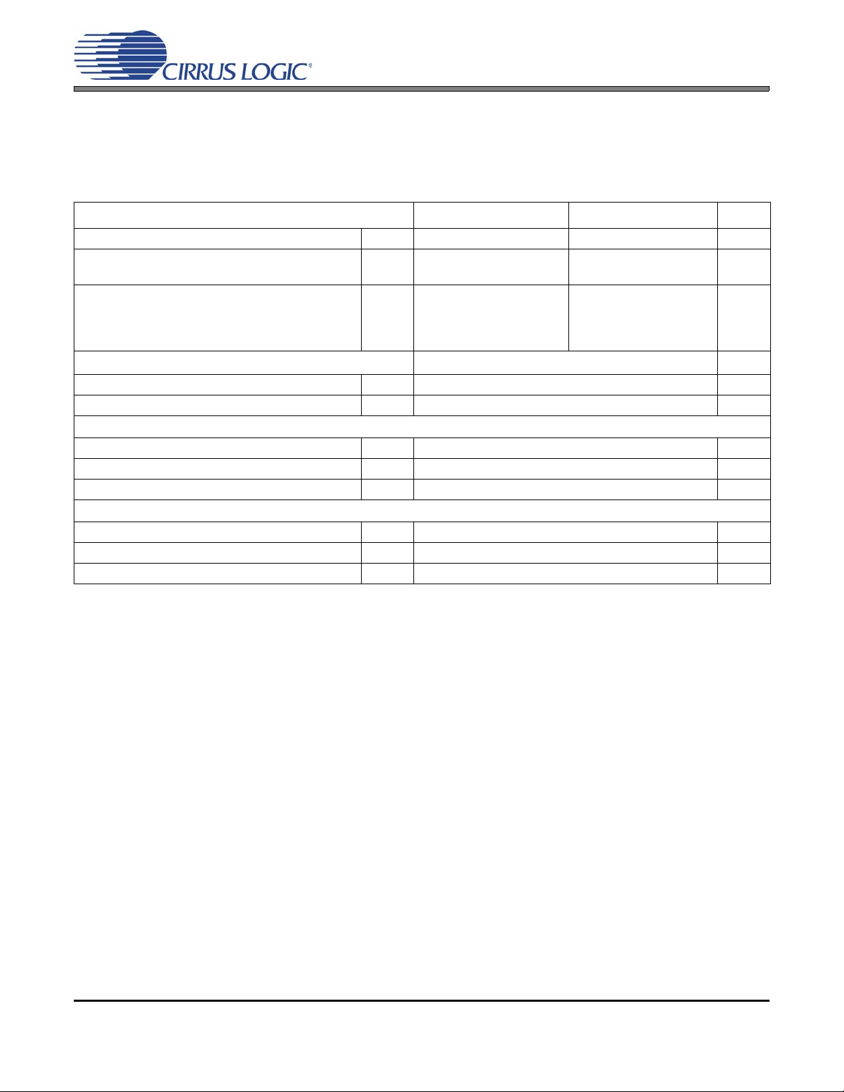
ANALOG CHARACTERISTICS - COMMERCIAL GRADE (-CZZ)
Test conditions (unless otherwise specified): TA = 25C; Input test signal is a 997 Hz sine wave through recommended inputs as seen in Figure 6 on page 14; source impedance less than or equal to 2.5 k; valid with FILT+
and VQ components as shown in Figure 3 on page 11; measurement bandwidth is 10 Hz to 20 kHz; Fs = 48 kHz
or 96 kHz.
Dynamic Performance for Commercial Grade
Symbol Min Typ Max Min Typ Max Unit
Dynamic Range A-weighted
unweighted
Total Harmonic Distortion + Noise (Note 4)
-1 dB
-20 dB
-60 dB
THD+N
Dynamic Performance for Commercial Grade
Interchannel Isolation - 90 - dB
VA = 3.3 V VA = 5.0 V
91
88
-
-
-
94
91
-89
-71
-31
-
-
-86
-
-
95
92
98
95
-
-
-
-92
-75
-35
-
-
-89
-
-
VA=3.3V and VA=5.0V
Min Typ Max Unit
dB
dB
dB
dB
dB
DC Accuracy
Interchannel Gain Mismatch - - 0.1 dB
Gain Error -3 - +3 %
Gain Drift -
100 - ppm/°C
Analog Input Characteristics
Full-scale Input Voltage VA = 3.3 V nom 0.560*VA 0.568*VA 0.575*VA Vpp
Full-scale Input Voltage VA = 5 V nom 0.552*VA 0.559*VA 0.567*VA Vpp
Input Impedance - 7.5 - M
Notes:
4. Referred to the typical full-scale input voltage
DS687F4 5
Page 6

Draft
2/1/11
CS5343/4
ANALOG CHARACTERISTICS - AUTOMOTIVE GRADE (-DZZ)
Test conditions (unless otherwise specified): TA = -40C to 85C; Input test signal is a 997 Hz sine wave through
recommended inputs as seen in Figure 6 on page 14; source impedance less than or equal to 2.5 k; valid with
FILT+ and VQ components as shown in Figure 3 on page 11; measurement bandwidth is 10 Hz to 20 kHz;
Fs = 48 kHz or 96 kHz.
Dynamic Performance for Automotive Grade
Symbol Min Typ Max Min Typ Max Unit
Dynamic Range A-weighted
unweighted
Total Harmonic Distortion + Noise (Note 5)
-1 dB
-20 dB
-60 dB
THD+N
Dynamic Performance for Automotive Grade
Interchannel Isolation - 90 - dB
VA = 3.1 to 3.5 V VA = 4.75 to 5.25 V
86
83
-
-
-
94
91
-88
-71
-31
-76
-
90
-
87
-
-
-
-
-
98
95
-91
-75
-35
-
-
-84
-
-
VA = 3.1 V to 3.5 V and VA = 4.75 V to 5.25 V
Min Typ Max Unit
dB
dB
dB
dB
dB
DC Accuracy
Interchannel Gain Mismatch - - 0.1 dB
Gain Error -3 - +3 %
Gain Drift -
100 - ppm/°C
Analog Input Characteristics
Full-scale Input Voltage VA = 3.1 V to 3.5 V 0.523*VA 0.567*VA 0.612*VA Vpp
Full-scale Input Voltage VA = 4.75V to 5.25 V 0.54 3*VA 0.560*VA 0.573*VA Vpp
Input Impedance - 7.5 - M
Notes:
5. Referred to the typical full-scale input voltage
6 DS687F4
Page 7
Draft
2/1/11
CS5343/4
DIGITAL FILTER CHARACTERISTICS
Parameter Symbol Min Typ Max Unit
All Speed Modes
Passband (-0.1 dB) 0 - 0.489 Fs
Passband Ripple -0.031 - 0.031 d B
Stopband 0.560 - - Fs
Stopband Attenuation 60 - - dB
Total Group Delay (Fs = Output Sample Rate) t
gd
-12/Fs- s
High-Pass Filter Characteristics
Frequency Response -3.0 dB
-0.13 dB (Note 6)
Phase Deviation @ 20Hz (Note 6) -10-Deg
Passband Ripple - - 0 dB
-120-
Hz
-
Hz
Notes:
6. Response shown is for Fs equal to 48 kHz. Filter characteristics scale with Fs.
DC ELECTRICAL CHARACTERISTICS
GND = 0 V, all voltages with respect to 0 V. MCLK=12.288 MHz; Master Mode.
Parameter Symbol
Power Supply Current (Normal Operation) I
Power Supply Current (Power-Down Mode) (Note 7) I
Power Consumption (Normal Operation)
(Power-Down Mode) (Note 7)
Parameter Symbol Min Typ Max Unit
Power Supply Rejection Ratio (1 kHz) (Note 8)
Nominal Voltage
V
Q
Output Impedance
Filt+ Nominal Voltage
Output Impedance
Maximum allowable DC current source/sink
Notes:
7. Device enters power-down mode when MCLK is held static.
8. Valid with the recommended capacitor values on FILT+ and VQ as shown in the Typical Connection
Diagram.
VA = 3.3 V VA = 5.0 V
Min Typ Max Min Typ Max Unit
A
A
-
-
PSRR - 65 - dB
- 11 15 - 12 17 mA
-10--40 - uA
-
36<150--
-
-
-
-
-
-
0.44xVA
25
VA
220
2.5
60
-
<1
85-mW
-
-
-
-
-
mW
V
k
V
k
uA
DS687F4 7
Page 8

Draft
2/1/11
DIGITAL CHARACTERISTICS
Parameter Symbol Min Typ Max Units
High-Level Input Voltage (% of VA) V
Low-Level Input Voltage (% of VA) V
High-Level Output Voltage at Io = 500 A(% of VA)
Low-Level Output Voltage at Io =500 A(% of VA)
Input Leakage Current I
IH
IL
V
OH
V
OL
in
CS5343/4
60 - - %
--30%
70 - - %
--15%
-10 - 10 A
8 DS687F4
Page 9

Draft
1
64 Fs
------------------
2/1/11
CS5343/4
SYSTEM CLOCKING AND SERIAL AUDIO INTERFACE
Logic “0” = GND = 0 V; Logic “1” = VA, CL = 20 pF.
Parameter Symbol Min Typ Max Unit
Master Mode
MCLK Period (Double-Speed, 384x Mode) t
(Double-Speed, 192x Mode) 48 - 60 ns
(Double-Speed, 256x Mode) 36 - 45 ns
(Double-Speed, 128x Mode) 72 - 90 ns
(Single-Speed, 768x Mode) 24 - 30 ns
(Single-Speed, 384x Mode) 48 - 60 ns
(Single-Speed, 512x Mode) 36 - 45 ns
(Single-Speed, 256x Mode) 72 - 90 ns
MCLK Duty Cycle 405060%
Output Sample Rate (Single-Speed)
(Double-Speed)
LRCK Duty Cycle - 50 - %
SCLK Duty Cycle - 50 - %
SDOUT valid before SCLK rising t
SDOUT valid after SCLK rising t
SCLK falling to LRCK edge t
clkw
Fs
stp
hld
slrd
Slave Mode
MCLK Period (Double-Speed, 384x Mode) t
(Double-Speed, 192x Mode) 48 - 60 ns
(Double-Speed, 256x Mode) 36 - 45 ns
(Double-Speed, 128x Mode) 72 - 90 ns
(Single-Speed, 768x Mode) 24 - 325 ns
(Single-Speed, 384x Mode) 48 - 651 ns
(Single-Speed, 512x Mode) 36 - 488 ns
(Single-Speed, 256x Mode) 72 - 976 ns
MCLK Duty Cycle 405060%
Input Sample Rate (Single-Speed)
(Double-Speed)
LRCK Duty Cycle 40 50 60 %
clkw
Fs
24 - 30 ns
43
86
10 - - ns
40 - - ns
-20 - 20 ns
24 - 30 ns
4
86
-
-
-
-
54
108
54
108
kHz
kHz
kHz
kHz
SCLK Period t
SCLK Duty Cycle 455055%
SDOUT valid before SCLK rising t
SDOUT valid after SCLK rising t
SCLK falling to LRCK edge t
sclkw
stp
hld
slrd
10 - - ns
40 - - ns
-20 - 20 ns
--ns
DS687F4 9
Page 10

Draft
Figure 1. CS5343 I²S Serial Audio Interface
tt
stp hld
MSB MSB-1
LRCK
SCLK
SDOUT
t
slrd
t
sclkw
Figure 2. CS5344 Left-Justified Serial Audio Interface
tt
stp hld
MSB MSB-1
LRCK
SCLK
SDOUT
t
slrd
t
sclkw
2/1/11
CS5343/4
10 DS687F4
Page 11

3. TYPICAL CONNECTION DIAGRAM
AINL
AINR
6
8
1
SDOUT
9
GND
7
VQ
VA
10
5
FILT+
2
SCLK
3
LRCK
4
MCLK
Audio
Processor/
System
Clocks
VA or
GND
VA
3.3 V to 5 V
CS5343/4
10 k
1
10 k
2
Analog Input
Conditioning
10 k
2
1 µF 0.1 µF
1 µF 0.1 µF
1 µF0.1 µF
See Figure 6 on
page 14
1
Pull-up to VA for Master Mode
Pull-down to GND for Slave Mode
2
Optional pull-up resistor for configuring clocks in Master Mode as
described in the “Master Mode Speed
Selection” section on page 13
Draft
2/1/11
CS5343/4
DS687F4 11
Figure 3. Typical Connection Diagram
Page 12

4. APPLICATIONS
4.1 Operation as Clock Master or Slave
The CS5343/4 supports operation as either a clock master or slave. As a clock master, the left/right and
serial clocks are synchronously generated on-chip and output on the LRCK and SCLK pins, respectively.
As a clock slave, the LRCK and SCLK pins are always inputs and require external generation of the left/right
and serial clocks. The selection of clo ck master or slave is made via a 10 k pull-up resistor from SDOUT
to VA for Master Mode selection or via a 10 kpull-down resistor from SDOUT to GND fo r Slave Mo de se-
lection, as shown in Table 1.
Mode Selection
Master Mode
Slave Mode
Table 1. Master/Slave Mode Selection
4.1.1 Slave Mode Operation
A unique feature of the CS5343/4 is the automatic selection of either Single- or Double-Spe ed Mode when
acting as a clock slave. The auto-mode selection feature supports all standard audio sample rates from
4 to 108 kHz. Please refer to Table 2 for supported sa mp le rate ranges in Slave Mode.
Draft
2/1/11
10 k pull-up resistor from SDOUT to VA
10 kpull-down resistor from SDOUT to GND
CS5343/4
Speed Mode
Single-Speed Mode
Double-Speed Mode
Table 2. Speed Modes and the Associated Sample Rates (Fs) in Slave Mode
MCLK/LRCK
Ratio
256x 64 4 - 54
512x 64 4 - 54
384x 48, 64 4 - 54
768x 48, 64 4 - 54
128x 64 86 - 108
256x 64 86 - 108
192x 48, 64 86 - 108
384x 48, 64 86 - 108
SCLK/LRCK
Ratio
Input Sample Rate Range (kHz)
12 DS687F4
Page 13

4.1.2 Master Mode Operation
As clock Master, the CS5343/4 generates LRCK and SCLK synchronously on-chip. Table 3 shows the
available sample rates and associated clock ratios in Master Mode.
Draft
2/1/11
CS5343/4
Speed Mode
Single-Speed Mode
Double-Speed Mode
Table 3. Speed Modes and the Associated Sample Rates (Fs) in Master Mode
MCLK/LRCK
Ratio
256x 64 43 - 54
512x 64 43 - 54
384x 64 43 - 54
768x 64 43 - 54
128x 64 86 - 108
256x 64 86 - 108
192x 64 86 - 108
384x 64 86 - 108
SCLK/LRCK
Ratio
Input Sample Rate Range (kHz)
4.1.2.1 Master Mode Speed Selection
During power-up in Master Mode, the LRCK and SCLK pins are inputs to configure speed mode and the
output clock ratio. The LRCK pin is pulled low internally to select Single-Speed Mode by default, but Double-Speed Mode is accessed with a 10 k pull-up resistor from LRCK to VA as shown in Table 4. Similarly, the SCLK pin is internally pulled-low by default to select a 256x/512x MCLK/LRCK ratio, but a
MCLK/LRCK ratio of 348x/768x is accessed with a 10 k pull-up resistor from SCLK to VA as shown in
Table 4. Following the power-up routine, the LRCK and SCLK pins become clock outputs.
Pin Resistor Option Clock Configuration
LRCK
SCLK
Internal Pull-Down to GND (100 k) Single-Speed Mode (default)
External Pull-Up to VA (10 k) Double-Speed Mode
Internal Pull-Down to GND (100 k) 128x/256x/512x MCLK/LRCK (default)
External Pull-Up to VA (10 k) 192x/384x/768x MCLK/LRCK
Table 4. Speed Mode Selection in Master Mode
4.1.3 Master Clock
The CS5343/4 requires a Master clock (MCLK) which runs the internal sampling circuits and digital filters.
There is an internal automatic MC LK divider which is activated based on the input frequency of MCLK.
This divider selection allows the high and low MCLK speeds in a given speed mode (i.e. 256x and 512x
in SSM). Table 4 lists some common audio output sample rates and the required MCLK frequency.
Master and Slave Mode
Sample Rate (kHz) Speed Mode
32 (*Slave Mode Only) SSM *8.192 *16.384 *12.288 *24.576
44.1 SSM 1 1.289 22.579 16.934 33.868
48 SSM 12.288 24.576 18.432 36.864
Sample Rate (kHz) Speed Mode
88.2 DSM 11.289 22.579 16.934 33.868
96 DSM 12.288 24.576 18.432 36.864
Table 5. Common MCLK Frequencies in Master and Slave Modes
DS687F4 13
MCLK(MHz) MCLK (MHz)
256x 512x 384x 768x
MCLK(MHz) MCLK (MHz)
128x 256x 192x 384x
Page 14

4.2 Serial Audio Interface
Figure 4. CS5343 I²S Serial Audio Interface
SDATA 23 22 8 7 23 22
SCLK
LRCK
23 226543210 8765432109 9
Left Channel Right Channel
Figure 5. CS5344 Left-Justified Serial Audio Interface
SDATA 23 22 7 6 23 22
SCLK
LRCK
23 225432108 7654321089 9
Left Channel RightChannel
Figure 6. CS5343/4 Analog Input Network
CS5343/4
AIN
Input
R1
R2
1 µF
180pF
C0G
The CS5343 output is serial data in I²S audio format and the CS5344 output is serial data in Left-Justified
audio format. Figures 4 and 5 show the I²S and Left-Justified data relative to SCL K and LRCK. Additionally,
Figures 1 and 2 display more information on the required timing for the serial audio interface format. For an
overview of serial audio interface formats, please refer to Cirrus Application Note AN282.
Draft
2/1/11
CS5343/4
4.3 Digital Interface
VA supplies power to both the analog and digital sections of the ADC, and also powers the serial port. Consequently, the digital interface logic level must equal VA to within the limits specified under “Digital Charac-
teristics” on page 8.
4.4 Analog Connections
The analog modulator samples the input signal at half of the inter nal master clock rate, or 6.14 4 MHz when
MCLK = 12.288 MHz. The digital filter will reject signals within the stopband of the filter. However, there is
no rejection for input signals which are multiples of the input sampling frequency (n
n=0,1,2,... Refer to Figure 6 which shows the recommended topology of the analog input network. The external shunt capacitor and internal input impedance form a single-pole RC filter to provide the appropriate
filtering of noise at the modulator sampling frequency. Additionally, the 180 pF capacitor acts as a charge
source for the internal sampling circuits . Ca pa cit ors of NPO or other high-quality dielectric will produce the
best results while capacitors with a large voltage coefficient (such as general-purpose ceramics) can degrade signal linearity.
6.144 MHz), where
14 DS687F4
Page 15

4.4.1 Component Values
R1 R2
R1 R2+
------------------------ -
R2
R1 R2+
------------------------ -
R1 R2+
Figure 7. CS5343/4 Example Analog Input Network
CS5343/4
AIN
Input
4.99 k
4.99 k
1 µF
180pF
C0G
Three parameters determine the values of resistors R1 and R2 as shown in Figure 6: source impedance,
attenuation, and input impedance. Table 6 shows the design equation used to determine these values.
• Source Impedance: Source impedance is defined as the impedance as seen from the ADC looking
back into the signal network. The ADC achieves optimal THD+N performance with a source impedance less than or equal to 2.5 k.
• Attenuation: The required attenuation factor depends on the magnitude of the input signal. The full-
scale input voltage is specified under “Analog Characteristics - Commercial Grade (-CZZ)” on page 5.
The user should select values for R1 and R2 such that the magnitude o f the incoming signal multiplied
by the attenuation factor is less than or equal to the full-scale input voltage of the device.
• Input Impedance: Input impedance is the impedance from the signal source to the ADC analog input
pins, including the ADC. Because the ADC’s input impedance (see the “Ana log Characteristics - Com-
mercial Grade (-CZZ)” table on page 5) is several orders of magnitude larger than the resistor values
typically used for the input attenuator, its contribution can be neglected when calculating the input impedance. Table 6 shows the input parameters and the associated design equations for the input attenuator.
Source Impedance
Draft
2/1/11
CS5343/4
Attenuation Factor
Input Impedance
T able 6. Analog Input Design Parameters
Figure 7 illustrates an example configuration using two 4.99 kresistors in place of R1 and R2. Based o n
the discussion above, this circuit provides an optimal interface for both the ADC and the signal source.
First, consumer equipment frequently requires an input impedance of 10 kwhich the 4.99 kresistors
provide. Second, this circuit will attenuate a typical line level voltage, 2 Vrms, to the full-scale input of the
ADC, 1 Vrms when VA = 5 V. Finally, at 2.5 kthe source impedance optimizes analog performance of
the ADC.
4.5 Grounding and Power Supply Decoupling
As with any high-resolution converter, designing with the CS5343/4 requires care ful attention to power supply and grounding arrangements if its potential performance is to be realized. Figure 3 shows the recommended power arrangements, with VA connected to a clean supply. Decoupling capacitors should be as
near to the ADC as possible, with the low value ceramic capacitor being the nearest. All signals, especially
clocks, should be kept away from the FILT+ and VQ pins in order to avoid unwanted coupling into th e modulators. The FILT+ and VQ decoupling capacitors, particularly the 0.1 µF, must be positioned to minimize
the electrical path from FILT+ to GND. The CDB5343 evaluation board demonstrates the optimum layout
and power supply arrangements. To minimize digital noise, connect the ADC digital outputs only to CMOS
inputs.
DS687F4 15
Page 16

4.6 Synchronization of Multiple Devices
Figure 8. Stopband Rejection Figure 9. Transition Band
-140
-130
-120
-110
-100
-90
-80
-70
-60
-50
-40
-30
-20
-10
0
0.0 0.1 0.2 0.3 0.4 0.5 0.6 0.7 0.8 0.9 1.0
Frequency (normalized to Fs)
Amplitude (dB)
-140
-130
-120
-110
-100
-90
-80
-70
-60
-50
-40
-30
-20
-10
0
0.40 0 .42 0.44 0.46 0.48 0.50 0.52 0.54 0.56 0.58 0.60
Frequency (normalized to Fs)
Amplitude (dB)
Figure 10. Transition Band (Detail) Figure 11. Passband Ripple
-0.10
-0.08
-0.06
-0.04
-0.02
0.00
0.02
0.04
0.06
0.08
0.10
0.00 0 .05 0.10 0.15 0.20 0.25 0.30 0 .35 0.40 0.45 0.50
Frequency (normalized to Fs)
Amplitude (dB)
-10
-9
-8
-7
-6
-5
-4
-3
-2
-1
0
0.46 0.47 0.48 0.49 0.50 0.51 0.52
Frequency (normalized to Fs)
Amplitude (dB)
In systems where multiple ADCs are required, care must be taken to achieve simultaneous sampling. To
ensure synchronous sampling, the MCLK, SCLK, and LRCK signals must be the same for all of the CS5343
and CS5344 devices in the system.
5. FILTER PLOTS - ALL SPEED MODES
Draft
2/1/11
CS5343/4
16 DS687F4
Page 17

6. PARAMETER DEFINITIONS
Dynamic Range
The ratio of the rms value of the signal to the rms sum of all other spectral components over the spec ified
bandwidth. Dynamic Range is a signal-to-noise ratio measurement over the specified bandwidth made with
a -60 dBFS signal. 60 dB is added to resulting measurement to refer the measurement to full-scale. This
technique ensures that the distortion components ar e below the n oise level an d do n ot affect the m easu rement. This measurement technique has been accepted by the Audio Engineering Society, AES17-1991,
and the Electronic Industries Association of Japan, EIAJ CP-307. Expressed in decibels.
Total Harmonic Distortion + Noise
The ratio of the rms value of the signal to the rms sum of all other spectral components over the spec ified
bandwidth (typically 10 Hz to 20 kHz), including distortion components. Expressed in decibels. Measured
at -1 and -20 dBFS as suggested in AES17-1991 Annex A.
Frequency Response
A measure of the amplitude response variation from 10 Hz to 20 kHz relative to the amplitude response at
1 kHz. Units in decibels.
Interchannel Isolation
Draft
2/1/11
CS5343/4
A measure of crosstalk between the left and right channels. Measured for each channel at the conver ter's
output with no signal to the input under test and a full-scale signal applied to the other channel. Un its in decibels.
Interchannel Gain Mismatch
The gain difference between left and right channels. Units in decibels.
Gain Error
The deviation from the nominal full-scale analog input for a full-scale digital output.
Gain Drift
The change in gain value with temperature. Units in ppm/°C.
DS687F4 17
Page 18

7. PACKAGE DIMENSIONS
10LD TSSOP (3 mm BODY) PACKAGE DRAWING (Note 1)
E
N
1
23
e
b
A1
A2
A
D
SEATING
PLANE
E1
1
L
SIDE VIEW
END VIEW
TOP VIEW
L1
c
Draft
2/1/11
CS5343/4
INCHES MILLIMETERS
DIM MIN NOM MAX MIN NOM MAX
A -- -- 0.0433 -- -- 1.10
A1 0 -- 0.0059 0 -- 0.15
A2 0.0295 -- 0.0374 0.75 -- 0.95
b 0.0059 -- 0.0118 0.15 -- 0.30 4, 5
c 0.0031 -- 0.0091 0.08 -- 0.23
D -- 0.1181 BSC -- -- 3.00 BSC -- 2
E -- 0.1929 BSC -- -- 4.90 BSC -E1 -- 0.1181 BSC -- -- 3.00 BSC -- 3
e -- 0.0197 BSC -- -- 0.50 BSC --
L 0.0157 0.0236 0.0315 0.40 0.60 0.80
L1 -- 0.0374 REF -- -- 0.95 REF - -
µ0°--8°0°--8°
Controlling Dimension is Millimeters
Notes:
1. Reference document: JEDEC MO-187
2. D does not include mold flash or protrusions, which is 0.15 mm max. per side.
3. E1 does not include inter-lead flash or protrusions, which is 0.15 mm max per side.
4. Dimension b does not include a tota l allowa b le da m ba r pr ot ru sio n of 0. 08 mm max .
5. Exceptions to JEDEC dimension.
NOTE
THERMAL CHARACTERISTICS
Parameter Symbol Min Typ Max Unit
Allowable Junction Temperature T
Junction to Ambient Thermal Impedance
(4-layer PCB)
(2-layer PCB)
J
JA-4
JA-2
--135
-
-
100
170
-
-
C/W
C/W
18 DS687F4
C
Page 19

Draft
2/1/11
CS5343/4
8. ORDERING INFORMATION
Product Description Package Pb-Free Grade Temp Range Container Order #
98 dB, Multi-Bit Audio
CS5343
CS5343
CS5344
CS5344
CDB5343 CS5343 Evaluation Board - No - - - CDB5343
A/D Converter,
I²S Audio Format
98 dB, Multi-Bit Audio
A/D Converter,
I²S Audio Format
98 dB, Multi-Bit Audio
A/D Converter,
Left-Justified Audio Format
98 dB, Multi-Bit Audio
A/D Converter,
Left-Justified Audio Format
10-TSSOP Yes Commercial -40° to +85° C
10-TSSOP Yes Automotive -40° to +105° C
10-TSSOP Yes Commercial -40° to +85° C
10-TSSOP Yes Automotive -40° to +105° C
Rail CS5343-CZZ
Tape & Reel CS5343-CZZR
Rail CS5343-DZZ
Tape & Reel CS5343-DZZR
Rail CS5344-CZZ
Tape & Reel CS5344-CZZR
Rail CS5344-DZZ
Tape & Reel CS5344-DZZR
DS687F4 19
Page 20

Draft
2/1/11
9. REVISION HISTORY
Release Changes
Updated “Recommended Operating Conditions” on page 4
Updated specifications and limits for “Analog Characteristics - Commercial Grade (-CZZ)” on page 5
Updated specifications and limits for “Analog Characteristics - Automotive Grade (-DZZ)” on page 6
F1
F2
F3
F4
Corrected “Power Supply Current (Normal Operation)” on page 7
Increased specification for Slave-Mode “SDOUT valid after SCLK rising” on page 9
Corrected Section 4.1.2.1 on page 13
Updated Section 4.1.3 on page 13
Removed Fs < 43 kHz from master mode operation:
-Updated master mode timing specifications in the “System Clocking and Serial Audio Interface” on page 9
-Updated Input Sample Rate Range in Tabl e 3 on page 13
-Added note for “slave mode only” for Fs = 32 kHz in Table 5 on page 13.
Updated Passband Ripple, Stopband Attenuation and Total Group Delay specs in “Digital Filter Characteristics”
on page 7.
Corrected a typographical error in Table 5, “Common MCLK Frequencies in Master and Slave Modes,” on
page 13. Changed 8.912 MHz to 8.192 MHz.
CS5343/4
20 DS687F4
Page 21

Draft
Contacting Cirrus Logic Support
For all product questions and inquiries, contact a Cirrus Logic Sales Representative.
To find one nearest you, go to www.cirrus.com.
IMPORTANT NOTICE
Cirrus Logic, Inc. and its subsidiaries (“Cirrus”) believe that the information contained in this document is accurate and reliable. However, the information is subject
to change without noti ce and is provided “AS IS” wi thout war ranty of any kind (express or impli ed). Cust omers ar e advise d to obtain the latest version of relevant
information to verify, before placing orders, that information being relied on is current and complete. All products are sold subject to the terms and conditions of sale
supplied at the time of order acknowled gment, includin g those pertaining to wa rranty, indemnificatio n, and limitation of liability. No responsibility is assumed by Cirrus
for the use of this information, including use of this information as the basis for manufacture or sale of any items, or for infringement of patents or other rights of third
parties. This document is the property of Cirrus and by furnishing this information, Cirrus grants no licens e, e x press or implied under any patents, mask work rights,
copyrights, trademarks, trade secrets or other intellectual property rights. Cirrus owns the copyrights associated with the information contained herein and gives co nsent for copies to be made of the information only for use within your organization with respect to Cirrus integrated circuits or other products of Cirrus. This consent
does not extend to other copying such as copying for general distribution, advertising or promotional purposes, or for creating any work for resale.
CERTAIN APPLICATIONS USING SEMICONDUCTOR PRODUCTS MAY INVOLVE POTENTIAL RISKS OF DEATH, PERSONAL INJURY, OR SEVERE PROPERTY OR ENVIRONMENTAL DAMAGE (“CRITICAL APPLICATIONS”). CIRRUS PRODUCTS ARE NOT DESIGNED, AUTHORIZED OR WARRANTED FOR USE
IN PRODUCTS SURGICALLY IMPLANTED INTO THE BODY, AUTOMOTIVE SAFETY OR SECURITY DEVICES, LIFE SUPPORT PRODUCTS OR OTHER CRITICAL APPLICATIONS. INCLUSION OF CIRRUS PRODUCTS IN SUCH APPLICATIONS IS UNDERSTOOD TO BE FULLY AT THE CUSTOMER’S RISK AND CIRRUS DISCLAIMS AND MAKES NO WARRANTY, EXPRESS, STATUTORY OR IMPLIED, INCLUDING THE IMPLIED WARRANTIES OF MERCHANTABILITY AND
FITNESS FOR PARTICULAR PURPOSE, WITH REGARD TO ANY CIRRUS PRODUCT THAT IS USED IN SUCH A MANNER. IF THE CUSTOMER OR CUSTOMER’S CUSTOMER USES OR PERMITS THE USE OF CIRRUS PRODUCTS IN CRITICAL APPLICATIONS, CUSTOMER AGREES, BY SUCH USE, TO FULLY
INDEMNIFY CIRRUS, ITS OFFICERS, DI RECTORS, EMPL OYEES, DIST RIBUT ORS AND OTHER AGENTS FROM ANY AND ALL LIABILITY, INCLUDING ATTORNEYS’ FEES AND COSTS, THAT MAY RESULT FROM OR ARISE IN CONNECTION WITH THESE USES .
Cirrus Logic, Cirrus, and the Cirrus Logic logo designs are trademarks of Cirrus Logic, Inc. All other brand and product names in this document may be trademarks
or service marks of their respective owners.
2/1/11
CS5343/4
DS687F4 21
 Loading...