

Page 1
FEATURES
• 32-bit Post-Processor Audio DSP supports Multichannel
®
Dolby
Volume
•
Programmable through DSP Composer
• CS49DV8, supports up to 7.1 Channels of Dolby Volume
processing at 48 kHz, 44.1 kHz or 32 kHz.
— I n put C onf igu rab le for all input/output d igi t al au dio ty pes
2
(I
S, LJ/RJ, and TDM)
— 32-bit data path deli ve rs uncompromised dynamic rang e
— 192 kHz capable integrated S/PDIF transmitter
— DAO can operate in master or slave mode (SCLK &
LRCLK)
• Integrated Clock Manager/PLL
— Capable of operating from a wide variety of external
crystals or external oscillators
• Input Fs Auto Detection, Reporting and Handling
• Sample rate conversion.
• Master & Slave Host Boot Capability via Serial Interface
• SPI interface capable of running up to 25 MHz during run
time
• 1.8V Core and a 3.3V I/O that is tolerant to 5V input
™
CS49DV8C Data Sheet
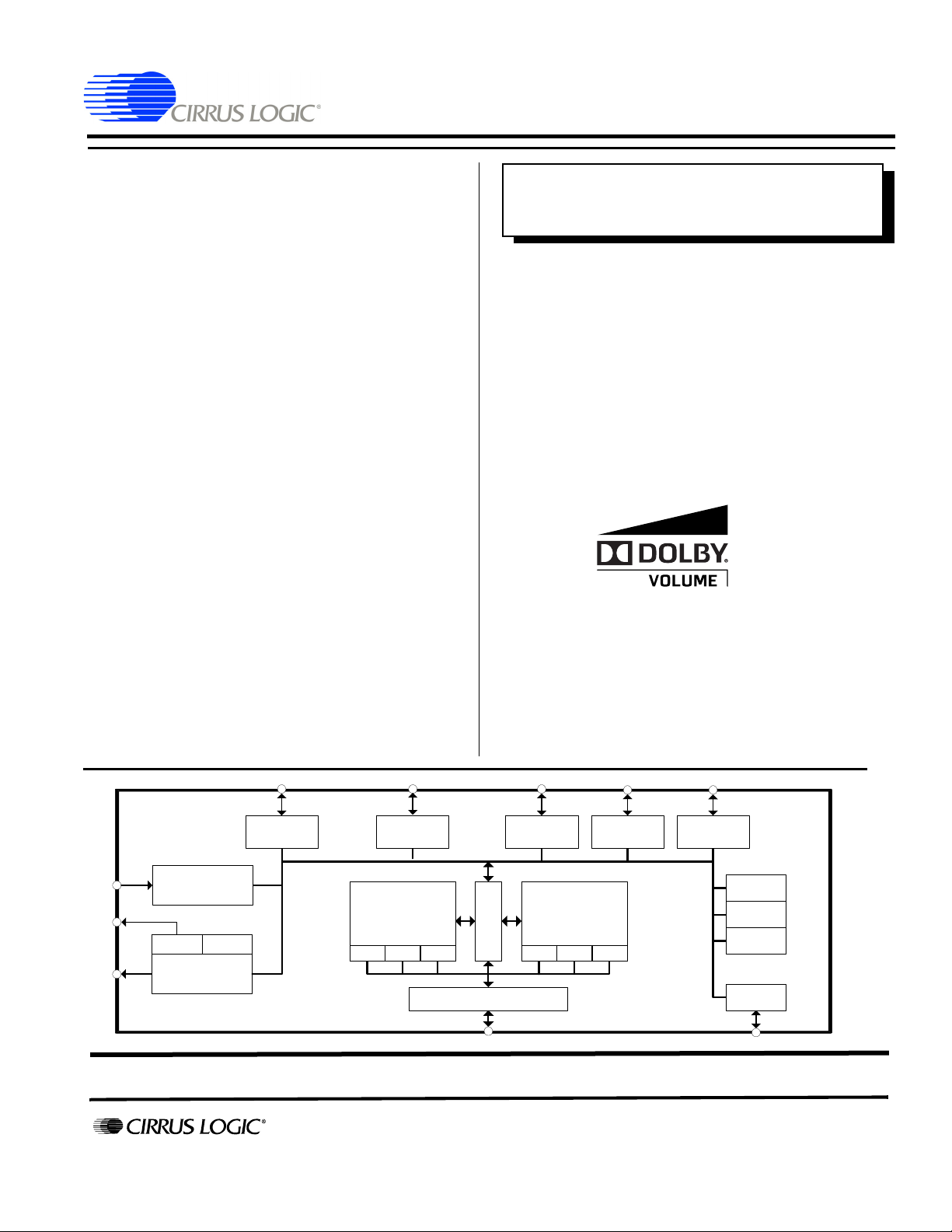
32-bit Dual Audio DSP Engine
featuring Multichannel Dolby
The new CS49DV8C is the fastest time-to-market, massproduction ready Multichannel Dolby Volume solution available.
The target applications for the CS49DV8C DSP are:
— Soundbars
— DTVs with Integrated Soundbars
— HDTV Stands/Furniture with Integrated Soundbars
— Automotive Head Units
— Automot ive Outboard Amplifiers
— Blu-ray Disc
All of these applications and many more that use volume control
and are subject to playback from sources that do not have consistent volume levels will benefit from the CS49DV8C Dolby Volume
solution.
®
& DVD Receivers / HTiBs
®
Volume
8 Ch. Audio In
S/PDIF
S/PDIF
8 Ch PCM
Audio Out
Serial
Control 1
Ordering Information
See page 27 for ordering information.
Serial
Control 2
32-bit
DSP A
P
X Y P X Y
Ext. Memory Controller
D
M
A
32-bit
DSP B
GPIOUART Debug
STC
TMR1
TMR2
PLL
Preliminary Product Information
Copyright 2008 Cirrus Logic (All Rights Reserved) SEPT ‘08
http://www.cirrus.com
This document contains information for a new product.
Cirrus Logic reserves the right to modify this product without notice.
DS868PP2
Page 2
CS49DV8C Data Sheet
32-bit Audio DSP Family
Contacting Cirrus Logic Support
For all product questions and inquiries contact a Cirrus Logic Sales Representative.
To find the one nearest to you go to
IMPORTANT NOTICE
“Preliminary” product inf orm ati on describes products that are in production, but for which ful l chara ct eri zati on data is not yet available. Cirrus Logic, Inc. and its sub-
sidiaries (“Cirrus”) bel i eve th at the in f ormat i on co nt ai ne d i n thi s document is accurate and reliable. However, the information is subject to change without noti ce and
is provided “AS IS” without warranty of any kind (express or implied). Customers are advised to obtain the latest version of relevant information to verify, before placing
orders, that information being relied on is current and complete. All products are sold subject to the terms and conditions of sale supplied at the time of order acknowledgment, includin g those p ertainin g to warra nty, inde mnific ation, and limitat ion of liab ility. No responsib ility is ass umed b y Cirrus for the use of this information, including use of this information as the basis for manufacture or sale of any items, or for infringement of patents or other rights of third parties. This document is the property
of Cirrus and by furnishing this information, Cirrus grants no license, express or implied under any patents, mask work rights, copyrights, trademarks, trade secrets or
other intellectual property rights. Cirrus owns the copyrights associated with the information contained herein and gives consent for copies to be made of the information only for use within your organization with respect to Cirrus integrated circuits or other prod uct s of Cirr us. Thi s consen t does not extend to other copying such as
copying for general distribution, advertising or promotional purposes, or for creating any work for resale.
CERTAIN APPLICATIONS USING SEMICO NDUCTOR PRODUCTS M AY INVOLVE P OTENTIAL RISKS OF DEATH, P ERSONAL INJURY, OR SEVERE PROPERTY OR ENVIRONMENTAL DAMAGE (“CRITICAL APPLICATIONS”). CIRRUS PRODUCTS ARE NOT DESIGNED, AUTHORIZED OR WARRANTED FOR USE IN
PRODUCTS SURGICALLY IMPLANT ED INTO THE BODY, AUTOMOTIVE SA FETY OR SECURITY DEVICES, LIFE SUPPORT PRODUCT S OR OTHER CRITICAL
APPLICATIONS. INCLUSION OF CIRRUS PRODUCTS IN SUCH APPLICATIONS IS UNDERSTOOD TO BE FULLY AT THE CUSTOMER'S RISK AND CIRRUS
DISCLAIMS AND MAKES NO WARRANTY, EXPRES S, STATUT ORY OR IM PLIED, INCLUDING THE IMPLIED WA RRANTIES O F MER CHANTABILIT Y AND FITNESS FOR PARTICULAR PURPOSE, W ITH REGARD TO ANY CIRR US PRODUCT THAT IS USED IN SUCH A MANNER. IF THE CUSTOM ER OR CUSTOMER'S
CUSTOMER USES OR PERMITS THE USE OF CIRRUS PRODUCTS IN CRITICAL APPLICATIONS, CUSTOMER AGREES, BY SUCH USE, TO FULLY INDEMNIFY CIRRUS, ITS OFFICERS, DIRECTORS, EMPLO YEES, DISTRIBUTO RS AND OTHER AG ENTS FROM ANY AND ALL LIAB ILITY, INCLUDING ATTO RNEYS'
FEES AND COSTS, THAT MAY RESULT FRO M OR ARISE IN CONNECTION WITH THESE USES.
Cirrus Logic, Cirrus, the Cirrus Logic logo designs, DSP Composer, and Cirrus Framework are trademarks of Cirrus Logic, Inc. All other brand and product names in
this document may be trademarks or service marks of their respective owners.
Dolby is a registered trademarks of Dolby Laboratories, Inc. Dolby Volume is a trademark of Dolby Laboratories, Inc. Supply of an implementation of Dolby Technology
does not convey a license nor imply a right under any patent, or any other industrial or Intellectual Property Right of Dolby Laboratories, to use the Implementation in
any finished end-user or ready-to-use final product. It is hereby notified that a license for such use is required from Dolby Laboratories.
Motorola and SPI are trademarks of Motorola, Inc.
2
I
C is a registered trademark of Philips Semiconductor.
Logic7 is a registered trademark of Harmon International Industries, Inc.
iPod is a registered trademark of Apple Computer, Inc.
Blu-ray
and Blu-ray Disc are trademarks of SONY KABUSHIKI KAISHA CORPORATION .
www.cirrus.com
.
2 Copyright 2008 Cirrus Logic, Inc. DS868PP2
Page 3

CS49DV8C Data Sheet
32-bit Audio DSP Family
Table of Contents
1. Documentation Strategy ...................... ..... .... ..... ................................. .... ..... ..... ..............................5
2. Overview ............................ ..... ................................. .... ..... ................................. .... ..... ..... ................5
2.1 Licensing .........................................................................................................................................................7
3. Firmware Supported .......................................... ................................. .... ..... ................................. ..7
4. Hardware Functional Description ................................................ ..... .... ..... .............................. ... ..7
4.1 DSP Core ........................................................................................................................................................7
4.1.1 DSP Memory ......................................................................................................................................7
4.1.2 DMA Controller ...................................................................................................................................7
4.2 On-chip DSP Peripherals ................................................................................................................................8
4.2.1 Digital Audio Input Port (DAI) ..............................................................................................................8
4.2.2 Digital Audio Output Port (DAO) .........................................................................................................8
4.2.3 Serial Control Port 1 & 2 (I
4.2.4 External Memory Interface .................................................................................................................8
4.2.5 GPIO ...................................................................................................................................................8
4.2.6 PLL-based Clock Generator ...............................................................................................................8
4.3 DSP I/O Description ........................................................................................................................................9
4.3.1 Multiplexed Pins .................................................................................................................................9
4.3.2 Termination Requirements ..................................................................................................................9
4.3.3 Pads ...................................................................................................................................................9
4.4 Application Code Security ...............................................................................................................................9
2C®
or SPI™) ............................................................................................ 8
5. Characteristics and Specifications ................................ ..... ................................ ..... ...................10
5.1 Absolute Maximum Ratings ...........................................................................................................................10
5.2 Recommended Operating Conditions ...........................................................................................................10
5.3 Digital DC Characteristics .............................................................................................................................10
5.4 Power Supply Characteristics .......................................................................................................................11
5.5 Thermal Data (128-Pin LQFP) ...................................................................................................................... 11
5.6 Switching Characteristics— RESET ..............................................................................................................12
5.7 Switching Characteristics — XTI ...................................................................................................................13
5.8 Switching Characteristics — Internal Clock ...................................................................................................13
5.9 Switching Characteristics — Serial Control Port - SPI Slave Mode ..............................................................14
5.10 Switching Characteristics — Serial Control Port - SPI Master Mode ..........................................................15
5.11 Switching Characteristics — Serial Control Port - I
5.12 Switching Characteristics — Serial Control Port - I
5.13 Switching Characteristics — UART .............................................................................................................18
5.14 Switching Characteristics — Digital Audio Slave Input Port ........................................................................19
5.15 Switching Characteristics — Digital Audio Output Port ...............................................................................20
5.16 Switching Characteristics — SDRAM Interface ...........................................................................................22
2
C Slave Mode .............................................................16
2
C Master Mode ...........................................................17
6. Ordering Information ......................................... ................................. .... ..... .................................27
7. Environmental, Manufac turi ng, and Ha ndling Informa tion ........................................ ..... .... .....27
8. Device Pin-Out Diagram ................. ................................. ..... .... ................................. ..... ..... .........28
8.1 128-Pin LQFP Pin-Out Diagram.................................................................................................................... 28
9. Package Mechanica l Drawings .............................. .... ................................. ..... ............................29
9.1 128-Pin LQFP Package .................................................................................................................................29
10. Revision History ................... ..... ......... ......... .......... ......... ..... ......... ......... .......... ......... ..... ..... .... .....30
DS868PP2 Copyright 2008 Cirrus Logic, Inc. 3
Page 4

CS49DV8C Data Sheet
32-bit Audio DSP Family
List of Figures
Figure 1. RESET Timing . . . . . . . . . . . . . . . . . . . . . . . . . . . . . . . . . . . . . . . . . . . . . . . . . . . . . . . . . . . . . . . . . . . . . . . 12
Figure 2. XTI Timing . . . . . . . . . . . . . . . . . . . . . . . . . . . . . . . . . . . . . . . . . . . . . . . . . . . . . . . . . . . . . . . . . . . . . . . . . . 13
Figure 3. Serial Control Port - SPI Slave Mode Timing . . . . . . . . . . . . . . . . . . . . . . . . . . . . . . . . . . . . . . . . . . . . . . . . 14
Figure 4. Serial Control Port - SPI Master Mode Timing . . . . . . . . . . . . . . . . . . . . . . . . . . . . . . . . . . . . . . . . . . . . . . . 15
Figure 5. Serial Control Port - I
Figure 6. Serial Control Port - I
Figure 7. UART Timing . . . . . . . . . . . . . . . . . . . . . . . . . . . . . . . . . . . . . . . . . . . . . . . . . . . . . . . . . . . . . . . . . . . . . . . . 18
Figure 8. Digital Audio Input (DAI) Port Timing Diagram . . . . . . . . . . . . . . . . . . . . . . . . . . . . . . . . . . . . . . . . . . . . . . . 19
Figure 9. Digital Audio Port Timing Master Mode . . . . . . . . . . . . . . . . . . . . . . . . . . . . . . . . . . . . . . . . . . . . . . . . . . . . 20
Figure 10. Digital Audio Output Timing, Slave Mode (Relationship LRCLK to SCLK) . . . . . . . . . . . . . . . . . . . . . . . . 21
Figure 11. External Memory Interface - SDRAM Burst Read Cycle . . . . . . . . . . . . . . . . . . . . . . . . . . . . . . . . . . . . . . 23
Figure 12. External Memory Interface - SDRAM Burst Write Cycle . . . . . . . . . . . . . . . . . . . . . . . . . . . . . . . . . . . . . . 24
Figure 13. External Memory Interface - SDRAM Auto Refresh Cycle . . . . . . . . . . . . . . . . . . . . . . . . . . . . . . . . . . . . . 25
Figure 14. External Memory Interface - SDRAM Load Mode Register Cycle . . . . . . . . . . . . . . . . . . . . . . . . . . . . . . . 26
Figure 15. 128-Pin LQFP Pin-Out . . . . . . . . . . . . . . . . . . . . . . . . . . . . . . . . . . . . . . . . . . . . . . . . . . . . . . . . . . . . . . . . 28
Figure 16. 128-Pin LQFP Package Drawing . . . . . . . . . . . . . . . . . . . . . . . . . . . . . . . . . . . . . . . . . . . . . . . . . . . . . . . . 29
2
C Slave Mode Timing . . . . . . . . . . . . . . . . . . . . . . . . . . . . . . . . . . . . . . . . . . . . . . . . 16
2
C Master Mode Timing . . . . . . . . . . . . . . . . . . . . . . . . . . . . . . . . . . . . . . . . . . . . . . . 17
List of Tables
Table 1. CS49DV8C Related Documentation . . . . . . . . . . . . . . . . . . . . . . . . . . . . . . . . . . . . . . . . . . . . . . . . . . . . . . . . 5
Table 2. Device and Firmware Selection Guide. . . . . . . . . . . . . . . . . . . . . . . . . . . . . . . . . . . . . . . . . . . . . . . . . . . . . . . 6
Table 3. CS49DV8C DSP Memory Sizes. . . . . . . . . . . . . . . . . . . . . . . . . . . . . . . . . . . . . . . . . . . . . . . . . . . . . . . . . . . . 7
Table 4. Ordering Information. . . . . . . . . . . . . . . . . . . . . . . . . . . . . . . . . . . . . . . . . . . . . . . . . . . . . . . . . . . . . . . . . . . . 27
Table 5. Environmental, Manufacturing, and Handling Information . . . . . . . . . . . . . . . . . . . . . . . . . . . . . . . . . . . . . . . 27
Table 6. 128-Pin LQFP Package Characteristics. . . . . . . . . . . . . . . . . . . . . . . . . . . . . . . . . . . . . . . . . . . . . . . . . . . . . 29
4 Copyright 2008 Cirrus Logic, Inc. DS868PP2
Page 5

CS49DV8C Data Sheet
32-bit Audio DSP Family
1. Documentation Strategy
The CS49DV8C data sheet describes the CS49DV8C family of multichannel audio DSPs. This
document should be used in conjunction with the following documents when evaluating or designing a
system around the CS49DV8C family of processors.
Table 1. CS49DV8C Related Documentation
Document Name Description
CS49DV8C Data Sheet This document
Detailed system design information including Typical
CS4953xx Hardware User’s Manual
Connection Diagrams, boot-procedures, pin
descriptions, and other system configuration
information.
Application note contains an Application
Programming Interface (API) used to control the
Dolby Volume firmware.
Includes detailed configuration and usage
information for the GUI development tool.
AN288PPH, “Dolby
DSP Composer
®
Volume Module”
™
User’s Manual
The scope of the CS49DV8C Data Sheet is primarily the hardware specifications of the CS49DV8C
devices. This includes hardware functionality, characteristic data, pinout, and packaging info rmation.
The intended audience for the CS49DV8C Data Sheet is the system PCB designer, MCU programmer,
and the quality control engineer.
2. Overview
The CS49DV8C DSP is designed to provide high-performance volume control using the Dolby Volume
algorithm. The CS49DV8, supports up to 7.1 Channels of Dolby Volume processing at 48 kHz, 44.1 kHz
or 32 kHz while leaving the 2nd core of the DSP completely available for even further processing
functions such as Quadruple Crossover Bass Management, Tone Control, and Multiband Parametric
EQ.
The CS49DV8C DSP, together with Cirrus Logic’s comprehensive li brary of audio pro cessing algorith ms,
enables the development of next-generation high-definition audio solutions. Cirrus Logic also provides a
broad array of digital interface products, and audio converters, to meet your audio system-level design
requirements.
The CS49DV8C is available in a 128-pin LQFP package.
Please refer to Table 2 on page 6 for the processor speed and available firmware for the CS49DV8C
product family.
DS868PP2 Copyright 2008 Cirrus Logic, Inc. 5
Page 6

DS868PP2 Copyright 2008 Cirrus Logic, Inc. 6
Table 2. Device and Firmware Selection Guide
Device
Pre-
Process
Decode Processor A
1
Mid-processor A
1
Mid-processor B
1
Post-processor
• Tone Control
CS49DV8C
300 MIPS
None
• Ste r eo PCM
• Multi-Channel PCM
(2:1 Downsampling Option)
(4:1 Downsampling Option)
®
Dolby
Volume
(Runs on either DSP A or B)
See Section 3. for additional
concurrency information.
Dolby® Volume
(Runs on either DSP A or B)
See Section 3 . for a dditio nal
concurrency information.
• Re-EQ
• PEQ (up to 11 bands)
• Delay
• 7.1 Bass Manager
• Audio Manager
• 1:2 Upsampling
1. Processing may be restricted and dependent on firmware selected. Contact your Cirrus Logic FAE for concurrency matrix.
1
32-bit Audio DSP Family
CS49DV8C Data Sheet
Page 7
CS49DV8C Data Sheet
32-bit Audio DSP Family
2.1 Licensing
Licenses are required for Dolby Volume and for all of the third party audio processing algorithms. Please
contact your local Cirrus Sales representative for more information.
3. Firmware Supported
The suite of software available for the CS49DV8C family consists of operating systems (OS) and a
library of overlays. The overlays have been divided into three main groups called Decoders, Midprocessors, and Post-processors. All software components are defined as follows:
• OS/Kernel - Encompasses all non-audio processing tasks, including loading data from external
memory, processing host messages, calling audio-processing subroutines, auto-detection, error
concealment, etc.
• Dolby V ol ume - The CS49DV8C can run Dolby Volume on either DSP A or DSP B. On the DSP that
is not running Dolby Volume, it can run the firmware currently available on the CS4953xx family for
that DSP (A or B).
4. Hardware Functional Description
4.1 DSP Core
The CS49DV8C is a dual-core DSP with separate X and Y data and P code memory spaces. Each core
is a high-performance, 32-bit, user-programmable, fixed-point DSP that is capable of performing two
memory access control (MAC) operations per cl ock cycle. Each core has eight 72-bit accumulat ors, four
X- and four Y-data registers, and 12 index registers.
Both DSP cores are coupled to a flexible DMA engine. The DMA engine can move data between
peripherals such as the digi tal audio input (DAI) and digital audio output (DAO), external memory, or any
DSP core memory, all without the intervention of the DSP. The DMA engine offloads data move
instructions from the DSP core, leaving more MIPS available for signal processing instructions.
CS49DV8C functionality is controlled by application codes that are stored in on-board ROM or
downloaded to the CS49DV8C from a host MCU or external FLASH/EEPROM. Users c an choos e to use
standard audio post-processor modules which are available from Cirrus Logic.
4.1.1 DSP Memory
The memory maps for the DSPs are as follows. All memory sizes are composed of 32-bit words.
Table 3. CS49DV8C DSP Memory Sizes
Memory
Type
X 16k SRAM, 32k ROM 10k SRAM, 8k ROM
DSP A DSP B
Y 24k SRAM, 32k ROM 16k SRAM, 16k ROM
P 8k SRAM, 32k ROM 8k SRAM, 24k ROM
4.1.2 DMA Controller
The powerful 12-channel DMA controller can move data between 8 on-chip resources. Each resource
has its own arbiter: X, Y, and P RAM/ROMs on DSP A; X, Y, and P RAM/ROMs on DSP B; external
DS868PP2 Copyright 2008 Cirrus Logic, Inc. 7
Page 8

CS49DV8C Data Sheet
32-bit Audio DSP Family
memory; and the peripheral bus. Modulo and linear addressing modes are supported, with flexible start
address and increment controls. The service interval for each DMA channel as well as up to 6 interrupt
events, is programmable.
4.2 On-chip DSP Peripherals
4.2.1 Digital Audio Input Port (DAI)
The 12-channel (6 line) DAI port supports a wide variety of data input formats. The port is capable of
accepting PCM or IEC61937. Up to 32-bit word lengths are supported. Additionally support is provided
for audio data input to the DSP via the DAI from an HDMI receiver.
The port has two independent slave-only clock domains. Each dat a input can be independen tly assigned
to a clock domain. The sample rate of the input clock domains can be determined automatically by the
DSP, which off-loads the task of monitoring the SPDIF receiver from the host. A time-stamping feature
allows the input data to be sample-rate converted via software.
4.2.2 Digital Audio Output Port (DAO)
There are two DAO ports. Each port can output 8 channels of up to 32-bit PCM data. The port supports
data rates from 32 kHz to 192 kHz. Each port can be configured as an independent clock domain in
slave mode, or the ratio of the two clocks can be set to even mult iples of each other in master mode. The
two ports can also be ganged together into a single c lock domain. Each por t has one serial aud io pin that
can be configured as a 192 kHz SPDIF transmitter (data with embedded clock on a single line).
2C®
4.2.3 Serial Control Port 1 & 2 (I
or SPI™)
There are two on-chip seri al cont rol ports that are capabl e of oper ating as mas ter or slave in either I
SPI modes. SCP1 defaults to slave operation. It is dedicated for external host-control and supports an
external clock up to 25MHz in SPI mode. This high clock speed enables very fast code download,
control or data delivery. SCP2 defaults to master mode and is dedicated for booting from external serial
Flash memory or for audio sub-system control.
4.2.4 External Memory Interface
The external memory interface controller supports up to 128 Mbits of SDRAM, using a 16-bit data bus.
4.2.5 GPIO
Many of the CS49DV8C peripheral pins are multiplexed with GPIO. Each GPIO can be configured as an
output, an input, or an input with interrupt. Each input-pin interrupt can be configured as rising edge,
falling edge, active-low, or active-high.
4.2.6 PLL-based Clock Generator
The low-jitter PLL generates integer or fractional multiples of a reference frequency which are used to
clock the DSP core and peripherals. Through a second PLL divider chain, a dependent clock domain
can be output on the DAO port for driving audio converters. The CS49DV8C default s to runni ng from the
external reference frequency and can be switched to use the PLL output after overlays have been
loaded and configured, either through master boot from an external FLASH or through host control. A
built-in crystal oscillator circuit with a buffered output is provided. The buffered output frequency ratio is
selectable between 1:1 (default) or 2:1.
2
C or
8 Copyright 2008 Cirrus Logic, Inc. DS868PP2
Page 9

CS49DV8C Data Sheet
32-bit Audio DSP Family
4.3 DSP I/O Description
4.3.1 Multiplexed Pins
Many of the CS49DV8C pins are multi-functional. For details on pin functionality please refer to the
CS4953xx Hardware User’s Manual.
4.3.2 Termination Requirements
Open-drain pins on the CS49DV8C must be pulled high for proper operation. Please refer to the
CS4953xx Hardware User’s Manual to identify which pins are open-drain and what value of pull-up
resistor is required for proper operation.
Mode select pins on the CS49DV8C are used to select the boot mode upon the rising edge of reset. A
detailed explanation of termination requirements for each communication mode select pin can be found
in the CS4953xx Hardware User’s Manual.
4.3.3 Pads
The CS49DV8C I/O operates from the 3.3 V supply and is 5 V tolerant.
4.4 Application Code Security
The external program code may be encrypted by the programmer to protect any intellectual property it
may contain. A secret, customer-specific key is used to encrypt the program code that is to be stored
external to the device.
DS868PP2 Copyright 2008 Cirrus Logic, Inc. 9
Page 10

CS49DV8C Data Sheet
32-bit Audio DSP Family
5. Characteristics and Specifications
Note: All data sheet minimum and max im um timi ng p a ram ete rs are guaranteed over the rated voltage and tem pe r atu re. All
data sheet typical parameters are measured under the following conditions: T = 25 °C, C
VDDA = VDDIO = 3.3 V , GNDD = GNDIO = GNDA = 0 V.
5.1 Absolute Maximum Ratings
(GNDD = GNDIO = GNDA = 0 V; all voltages with respect to 0 V)
Parameter Symbol Min Max Unit
DC power supplies: Core supply
PLL supply
I/O supply
VDD
VDDA
VDDIO
|VDDA – VDDIO|
Input pin current, any pin except supplies I
Input voltage on PLL_REF_RES V
Input voltage on I/O pins V
Storage temperature T
in
filt
inio
stg
Caution: Operation at or be yond thes e limit s may resul t in per manent da mage to the device . Normal op eration is not
guaranteed at these extremes.
–0.3
–0.3
–0.3
-
-+/- 10mA
-0.3 3.6 V
-0.3 5.0 V
–65 150 °C
= 20 pF, VDD = 1.8 V,
L
2.0
3.6
3.6
0.3
V
V
V
V
5.2 Recommended Operating Conditions
(GNDD = GNDIO = GNDA = 0 V; all voltages with respect to 0 V)
Parameter Symbol Min Typ Max Unit
DC power supplies: Core supply
PLL supply
I/O supply
|VDDA – VDDIO|
Ambient operating temperature
Commercial Grade (CVZ/CVZ R)
Note:
It is recommended that the 3.3 V IO supply come up ahead of or simultaneously with the 1.8 V core supply.
5.3 Digital DC Characteristics
(Measurements performed under static conditions.)
Parameter Symbol Min Typ Max Unit
High-level input voltage V
Low-level input voltage, except XTI V
Low-level input voltage, XTI V
Input Hysteresis V
High-level output voltage (I
= -4mA), except XTI,
O
SDRAM pins
Low-level output voltage (I
= 4mA), except XTI,
O
SDRAM pins
SDRAM High-level output voltage (I
SDRAM Low-l evel output voltage (I
= -8mA) V
O
= 8mA) V
O
Input leakage current (all digital pins with internal
pull-up resistor s dis abl ed )
ILXTI
hys
V
OH
V
OL
OH
OL
I
IN
IH
IL
VDD
VDDA
VDDIO
1.71
3.13
3.13
1.8
3.3
3.3
1.89
3.46
3.46
0
T
A
0 +25 + 70 °C
2.0 - - V
--0.8V
--0.6V
0.4 V
VDDIO * 0.9 - - V
- - VDDIO * 0.1 V
VDDIO * 0.9 - - V
- - VDDIO * 0.1 V
--5μA
V
V
V
V
10 Copyright 2008 Cirrus Logic, Inc. DS868PP2
Page 11
Parameter Symbol Min Typ Max Unit
Input leakage current (all digital pins with internal
pull-up resistors enabled, and XTI)
5.4 Power Supply Characteristics
(Measurements performed under operating conditions.)
Parameter Min Typ Max Unit
Power supply cur r en t :
Core and I/O operating: VDD
1
PLL operating: VDDA
With external memory and most por ts operating : VDDIO
1.Dependent on application firmware and DSP clock speed.
5.5 Thermal Data (128-Pin LQFP)
Parameter Symbol Min Typ Max Unit
Thermal Resistance (Junction to Ambient)
Tw o-layer Board
Four-layer Board
Thermal Resistance (Junction to Top of Package)
Tw o-layer Board
Four-layer Board
I
IN-PU
1
2
1
2
θ
ψ
32-bit Audio DSP Family
--50μA
-
-
-
ja
-
-
jt
-
-
500
3.5
120
48
40
.39
.33
CS49DV8C Data Sheet
-
-
-
mA
mA
mA
°C / Watt
-
°C / Watt
-
-
Notes: 1.Two-layer bo ard is specifie d as a 76 mm X 114 mm , 1.6 mm thick FR-4 material with 1-oz copper c overing 20% of the top
and bottom layers.
2.Four-laye r board is specified as a 76mm X 114 mm, 1.6 mm thick FR-4 material wit h 1-oz co pper cov ering 20% of the top
and bottom layers and 0.5-oz copper covering 90% of the internal power plane and ground plane layers.
3.To calculate the die temperature for a given power dissipation
Τ
= Ambient Temperature + [ (Power Dissipation in Watts) * θja ]
j
4.To calculate the case temperature for a given power dissipation
Τ
= Τj - [ (Power Dissipation in Watts) * ψjt ]
c
DS868PP2 Copyright 2008 Cirrus Logic, Inc. 11
Page 12

CS49DV8C Data Sheet
32-bit Audio DSP Family
5.6 Switching Charac teristics— RESET
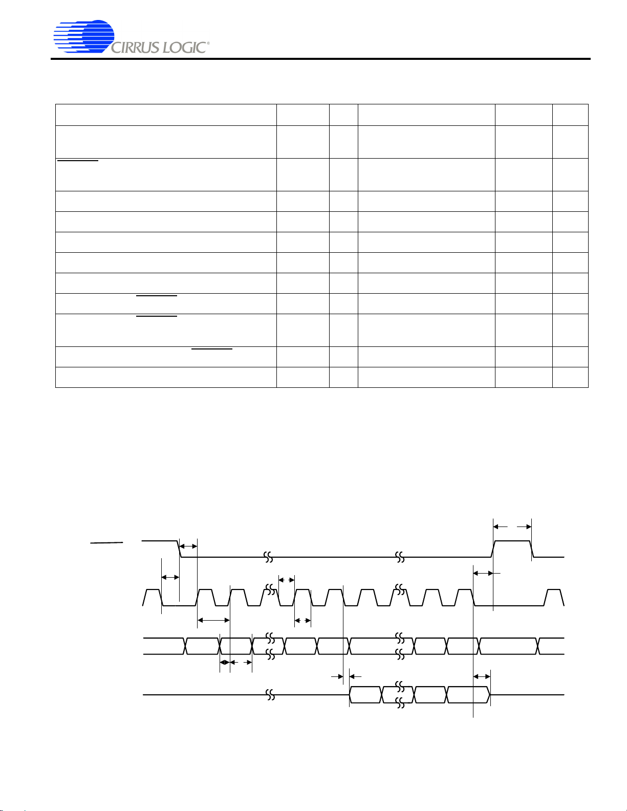
Parameter Symbol Min Max Unit
RESET
minimum pulse width low T
All bidirectional pins high-Z after RESET low T
Configuration pins setup before RESET
Configuration pins hold after RESET
high T
high T
RESET#
HS[3:0]
All Bidirectional
Pins
T
rst2z
T
rstl
T
rstl
rst2z
rstsu
rsthld
rstsu
T
1-μs
-100ns
50 - ns
20 - ns
rsthld
Figure 1. RESET Timing
12 Copyright 2008 Cirrus Logic, Inc. DS868PP2
Page 13

CS49DV8C Data Sheet
X
32-bit Audio DSP Family
5.7 Switching Characteristics — XTI
Parameter Symbol Min Max Unit
External Crystal operating frequency
XTI period T
XTI high time T
XTI low time T
External Crystal Load Capacitance (parallel resonant)
1
2
F
clkih
C
xtal
clki
clkil
11.2896 27 MHz
33.3 100 ns
13.3 - ns
13.3 - ns
L
10 18 pF
External Crystal Equivalent Series Resistance ESR 50 W
1. Part characterized with the following crystal frequency values: 11.2896, 12.288, 18.432, 24.576, and 27
MHz.
2. CL refers to the total load capacitance as specified by the crystal manufacturer . Crystals which require a
C
outside this range should be avoided. The crystal oscillator circuit design should follow the crystal
L
manufacturer’s recommendation for load capacitor selection.
TI
t
clkih
T
clki
Figure 2. XTI Timing
5.8 Switching Characteristics — Internal Clock
Parameter Symbol Min Max Unit
Internal DCLK frequency
Internal DCLK period
1.After initial power- on re se t, F
locked until the next power-on reset.
1
CS49DV8C-CVZ
CS49DV8C-CVZR
1
CS49DV8C-CVZ
CS49DV8C-CVZR
= F
dclk
. After initial kick st art c om m and s, the PLL is locked to max F
xtal
t
clkil
DCLKP
F
dclk
F
xtal
6.7 1/F
150
xtal
and remains
dclk
MHz
ns
DS868PP2 Copyright 2008 Cirrus Logic, Inc. 13
Page 14

CS49DV8C Data Sheet
32-bit Audio DSP Family
5.9 Switching Charac teristics — Serial Control Port - SPI Slave Mode
.
Parameter Symbol Min Typical Max Units
SCP_CLK frequency
1
f
spisck
-25MHz
SCP_CS falling to SCP_CLK rising t
SCP_CLK low time t
SCP_CLK high time t
Setup time SCP_MOSI input t
Hold time SCP_MOSI input t
SCP_CLK low to SCP_MISO output valid t
SCP_CLK falling to SCP_
IRQ rising t
SCP_CS rising to SCP_IRQ falling t
SCP_CLK low to SCP_CS
SCP_
CS rising to SCP_MISO output high-Z t
rising t
SCP_CLK rising t o SCP_BSY falling t
1. The specificati on f
actual maximum spee d of the communication port may be limited by the firmware application . Fl ow c ont rol us ing the
SCP_BSY
pin should be implemented to prevent overflow of the input data buffer.At boot the maximum speed is
Fxtal/3.
indicates the maximum speed of the hardw are. The sy stem desi gner should be aware that the
spisck
spicss
spickl
spickh
spidsu
spidh
spidov
spiirqh
spiirql
spicsh
spicsdz
spicbsyl
24 - ns
20 - ns
20 - ns
5-ns
5-ns
-11ns
-20ns
0ns
24 - ns
-20 ns
-3
DCLKP+20 ns
*
SCP_CS
SCP_CLK
SCP_MOSI
SCP_MISO
SCP_IRQ
SCP_BSY
t
spicss
t
t
spickh
spickl
t
spidov
MSB
56
t
spiirqh
7
LSB
t
spibsyl
12670
0
f
spisck
A6 A5 A0 R/W MSB LSB
t
spidsu
t
spidh
Figure 3. Serial Control Port - SPI Slave Mode Timing
t
spicsh
t
spicsdz
t
spiirql
14 Copyright 2008 Cirrus Logic, Inc. DS868PP2
Page 15
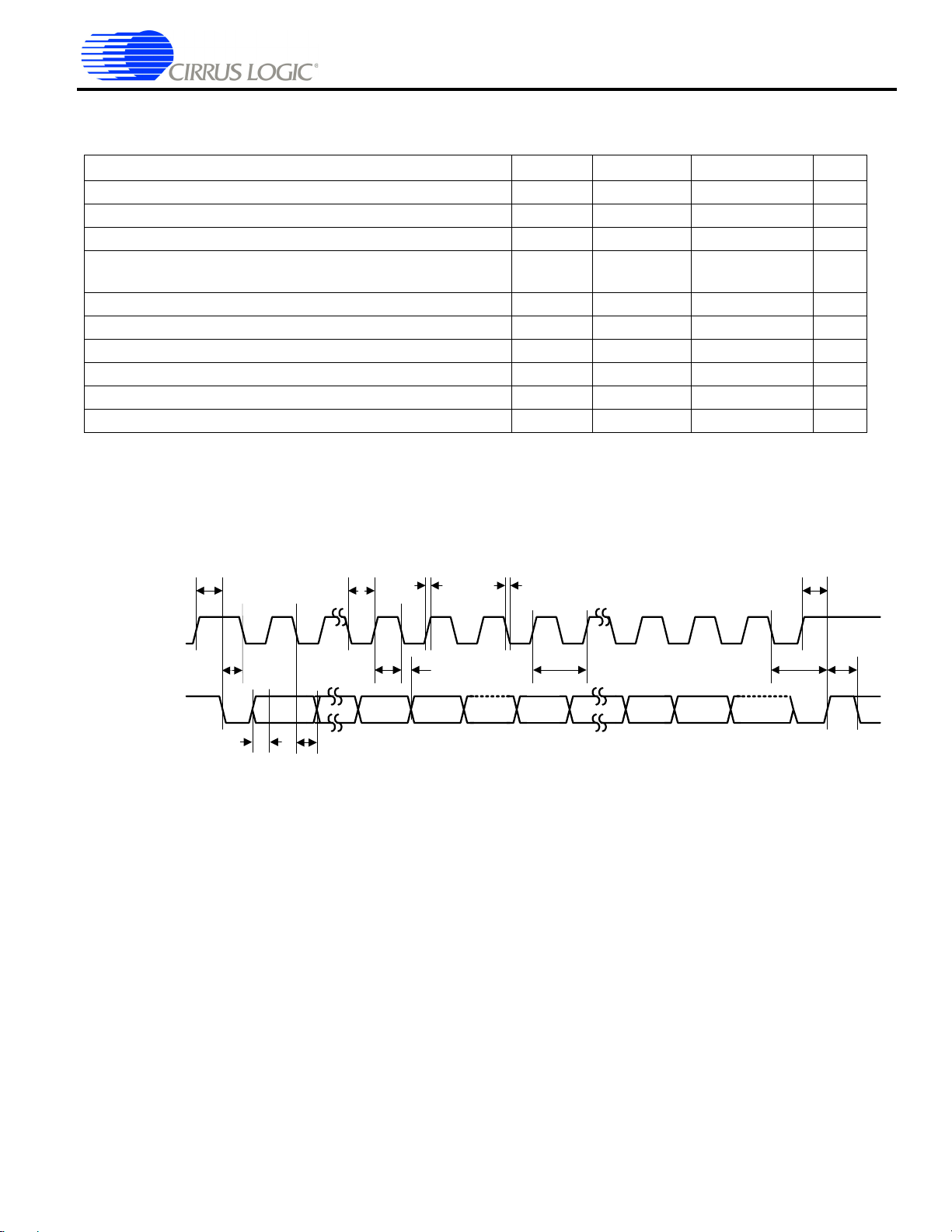
5.10 Switching Characteristics — Serial Control Port - SPI Master Mode
S
S
Parameter Symbol Min T ypical Max Units
SCP_CLK frequency
SCP_CS
falling to SCP_CLK rising
1
3
f
spisck
t
spicss
-F
- 11*DCLKP +
(SCP_CLK PERIOD)/2
CS49DV8C Data Sheet
32-bit Audio DSP Family
/2 (See
xtal
MHz
Footnote 2)
-ns
SCP_CLK low time t
SCP_CLK high time t
Setup time SCP_MISO input t
Hold time SCP_MISO input t
SCP_CLK low to SCP_MOSI output valid t
SCP_CLK low to SCP_CS falling t
SCP_CLK low to SCP_CS
rising t
spickl
spickh
spidsu
spidh
spidov
spicsl
spicsh
18 - ns
18 - ns
11 - ns
5-ns
-11ns
7-ns
- 11*DCLKP +
-ns
(SCP_CLK PERIOD)/2
Bus free time between active SCP_
CS t
SCP_CLK falling to SCP_MOSI output high-Z t
1. The specification f
indicates the maximum speed of the hardware. The system designer should be
spisck
spicsx
spidz
-20ns
3*DCLKP - ns
aware that the actual maximum speed of the communication port may be limited by the firmware
application.
2. See Section 5.7.
3. SCP_CLK PERIOD refers to the period of SCP_CLK as being used in a given application. It does not refer
to a tested parameter.
t
spicsx
t
spicss
EE_CS
t
spicsl
0
12670
spickl
56
7
t
spicsh
t
SCP_CLK
f
spisck
CP_MISO
A6 A5 A0 R/W MSB LSB
t
spidsu
t
spidh
CP_MOSI
DS868PP2 Copyright 2008 Cirrus Logic, Inc. 15
Figure 4. Serial Control Port - SPI Master Mode Timing
t
spickh
t
spidov
MSB
LSB
t
spidz
Page 16

CS49DV8C Data Sheet
ft
32-bit Audio DSP Family
5.11 Switching Characteristics — Serial Contr o l Port - I2C Slave Mode
Parameter Symbol Min Typical Max Units
SCP_CLK frequency
1
SCP_CLK low time t
SCP_CLK high time t
SCP_SCK rising to SCP_SDA rising or falling for
START or STOP condition
f
iicck
iicckl
iicckh
t
iicckcmd
- 400 kHz
1.25 - µs
1.25 - µs
1.25 µs
START condition to SCP_CLK falling t
SCP_CLK falling to STOP condition t
Bus free time between STOP and START conditions t
Setup time SCP_SDA input valid to SCP_CLK rising t
Hold time SCP_SDA input after SCP_CLK falling t
SCP_CLK low to SCP_SDA out valid t
SCP_CLK falling to SCP_IRQ
NAK condition to SCP_IRQ
SCP_CLK rising t o SCB_BSY
1. The specification f
actual maximum speed of the communication port may be limited by the firmware application. Flow control using the
SCP_BSY
pin should be implemented to prevent overflow of the input data buffer.
t
iicckcmd
rising t
low t
low t
indicates the ma ximu m spee d of the hardw are. The syste m des igner s hould b e awar e that th e
iicck
t
iicckl
01 67801 7
t
iicr
SCP_CLK
t
iicstscl
t
iicckh
t
iicdov
iicstscl
iicstp
iicbft
iicsu
iich
iicdov
iicirqh
iicirql
iicbsyl
t
iicf
1.25 - µs
2.5 - µs
3-µs
100 ns
20 - ns
-18ns
-3
DCLKP + 40 ns
*
3*DCLKP + 20 ns
-3*DCLKP + 20 ns
t
iicckcmd
8
t
iicstp
t
iicb
f
6
iicck
SCP_SDA
A6 A0 R/W ACK
t
iicsutiich
MSB
t
iicirqh
LSB
ACK
t
iicirql
SCP_IRQ
t
iiccbsyl
SCP_BSY
Figure 5. Serial Control Port - I2C Slave Mode Timing
16 Copyright 2008 Cirrus Logic, Inc. DS868PP2
Page 17
5.12 Switching Characteristics — Serial Control Port - I2C Master Mode
S
ft
Parameter Symbol Min Max Units
SCP_CLK frequency
SCP_CLK low time t
SCP_CLK high time t
SCP_SCK rising to SCP_SDA rising or falling for START or
STOP condition
START condition to SCP_CLK falling t
SCP_CLK falling to STOP condition t
Bus free time between STOP and START conditions t
Setup time SCP_SDA input valid t o SCP_CLK rising t
Hold time SCP_SDA input after SCP_CLK falling t
SCP_CLK low to SCP_SDA out valid t
1. The specificati on f
actual maximum speed of the communication port may be limited by the firmware application.
1
indicates the ma xi mu m speed of the h ardw a re. The s ys te m designer should b e a w are th at the
iicck
f
iicck
iicckl
iicckh
t
iicckcmd
iicstscl
iicstp
iicbft
iicsu
iich
iicdov
-400kHz
1.25 - µs
1.25 - µs
1.25 µs
1.25 - µs
2.5 - µs
3-µs
100 ns
20 - ns
-18ns
CS49DV8C Data Sheet
32-bit Audio DSP Family
CP_CLK
SCP_SDA
t
iicckcmd
t
iicstscl
t
iicckl
t
iicr
01 67801 7
t
iicckh
t
iicdov
A6 A0 R/W ACK
t
iicsutiich
t
iicf
6
f
iicck
MSB
Figure 6. Serial Control Port - I2C Master Mode Timing
LSB
8
ACK
t
iicstp
t
iicckcmd
t
iicb
DS868PP2 Copyright 2008 Cirrus Logic, Inc. 17
Page 18
CS49DV8C Data Sheet
U
32-bit Audio DSP Family
5.13 Switching Characteristics — UART
Parameter Symbol Min Max Unit
UART_CLK period
UART_CLK duty cycle - 40 60 %
Setup time for UART_RXD t
Hold time for UART_RXD t
Delay from CLK transition to TXD transition t
1. The minimum clock period is limited to DCLKP/32 or the minimum value, whichever is larger.
1
t
uclki
uckrxsu
uckrxdv
ucktxdv
266 - ns
55-ns
-29ns
UART_CLK
t
ucktxdv
t
txen
t
txhz
UART_TXD
UART_RXD
ART_TX_EN
t
uckrxsu
Figure 7. UART Timing
t
uckrxdv
18 Copyright 2008 Cirrus Logic, Inc. DS868PP2
Page 19

CS49DV8C Data Sheet
D
32-bit Audio DSP Family
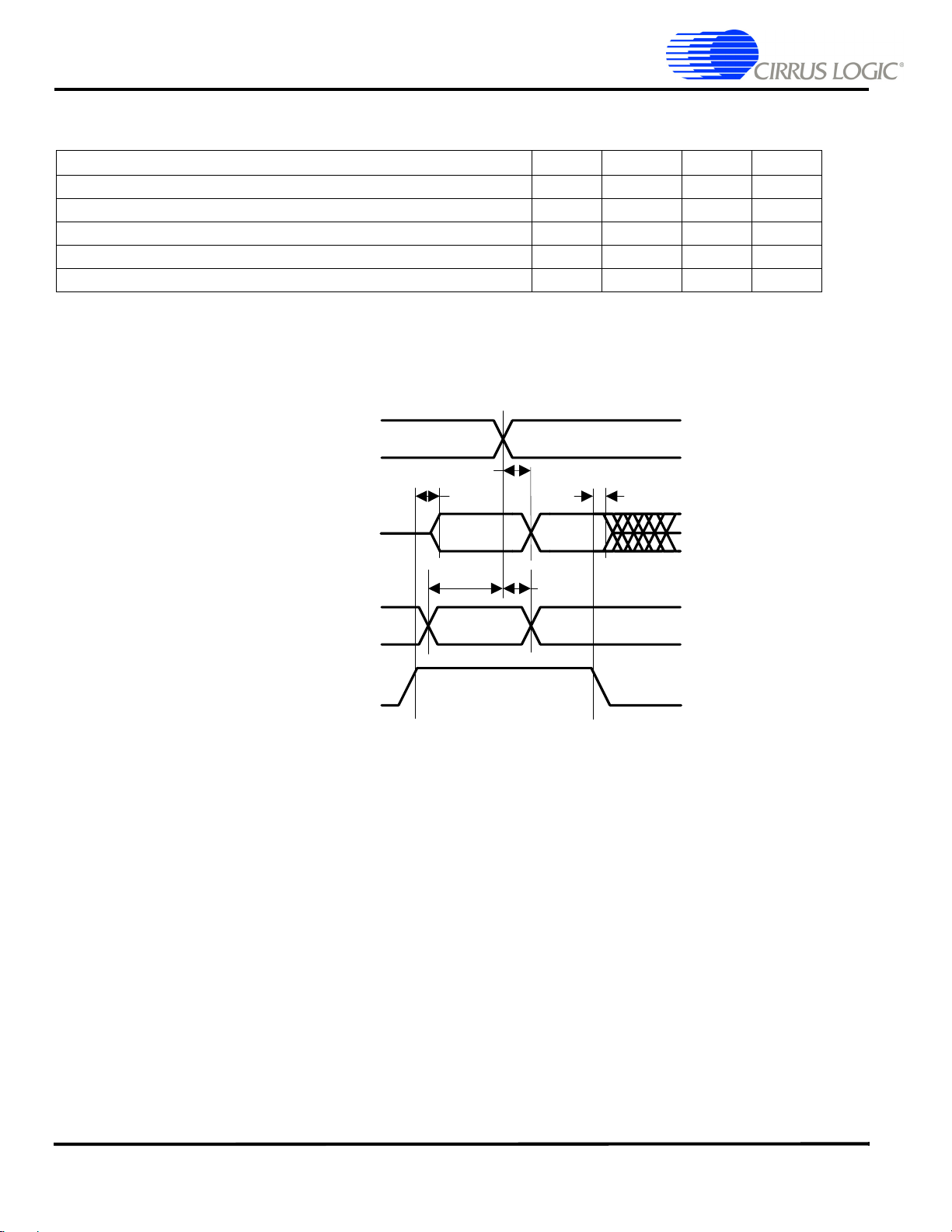
5.14 Switching Characteristics — Digital Audio Slave Input Port
Parameter Symbol Min Max Unit
DAI_SCLK period T
daiclkp
DAI_SCLK duty cycle - 45 55 %
Setup time DAI_DATAn t
Hold time DAI_DATAn t
daidsu
daidh
DAI_SCLK
t
daidsu
t
daidh
AI_DATAn
40 - ns
10 - ns
5-ns
Figure 8. Digital Audio Input (DAI) Port Timing Diagram
DS868PP2 Copyright 2008 Cirrus Logic, Inc. 19
Page 20

CS49DV8C Data Sheet
D
D
32-bit Audio DSP Family
5.15 Switching Characteristics — Digital Audio Output Port
Parameter Symbol Min Max Unit
DAO_MCLK period T
daomclk
DAO_MCLK duty cycle - 45 55 %
DAO_SCLK period for Master or Slave mode
DAO_SCLK duty cycle for Master or Slave mode
Master Mode (Output A1 Mode)
DAO_SCLK delay from DAO_MCLK rising edge,
1
1
1,2
T
daosclk
-4060%
t
daomsck
DAO_MCLK as an input
DAO_LRCLK delay from DAO_SCLK transition, respectively
DAO_SCLK delay from DAO_LRCLK transition, respectively
DAO1_DATA[3..0], DAO2_DATA[1..0]
delay from DAO_SCLK transition
Slave Mode (Output A0 Mode)
3
4
DAO1_DATA[3..0], DAO2_DATA[1..0]
delay from DAO_SCLK transition
3
DAO_LRCLK delay from DAO_SCLK transition, respectively
DAO_SCLK delay from DAO_LRCLK transition, respectively
1.Master mode timing specifications are characterized, not production tested.
2.Master mode is defined as the C S49DVxx drivin g both DAO_SCL K, DAO_LRCLK. Wh en MCLK is an in put, it is div ided
to produce DAO_SCLK, DAO_LRCLK.
3.This timing parameter is defined from the non-active edge of DAO_SCLK. The active edge of DAO_SCLK is the point
at which the data is valid.
4.Slave mode is defined as DAO_SCLK, DAO_LRCLK driven by an external source.
3
t
3
3
3
daomstlr
t
daomlrts
t
daomdv
t
daosdv
t
daosstlr
t
daoslrts
40 - ns
40 - ns
-19ns
-8ns
-8ns
-10ns
-15ns
-30ns
-15ns
t
DAO_MCLK
DAO_SCLK
t
AOn_DATAn
DAO_LRCLK
daomdv
daomlclk
DAO_MCLK
t
daomsck
DAO_SCLK
AOn_DATAn
t
daomlrts
DAO_LRCLK
t
daomclk
t
daomstlr
t
daomsck
Note: In these diagrams, Falling edge is the inactive edge of DAO_SCLK
Figure 9. Digital Audio Port Timing Master Mode
20 Copyright 2008 Cirrus Logic, Inc. DS868PP2
Page 21

DAO_LRCLK
D
D
D
v
DAO_SCLK
AOn_DATAn
Figure 10. Digital Audio Output Timing, Slave Mode (Relationship LRCLK to SCLK)
t
daosstlr
AO_LRCLK
AO_SCLK
t
daosclk
t
daoslrts
Note: In these diagrams, Falling edge is the inactive edge of DAO_SCLK
CS49DV8C Data Sheet
32-bit Audio DSP Family
t
daosclk
t
daosd
DS868PP2 Copyright 2008 Cirrus Logic, Inc. 21
Page 22

CS49DV8C Data Sheet
32-bit Audio DSP Family
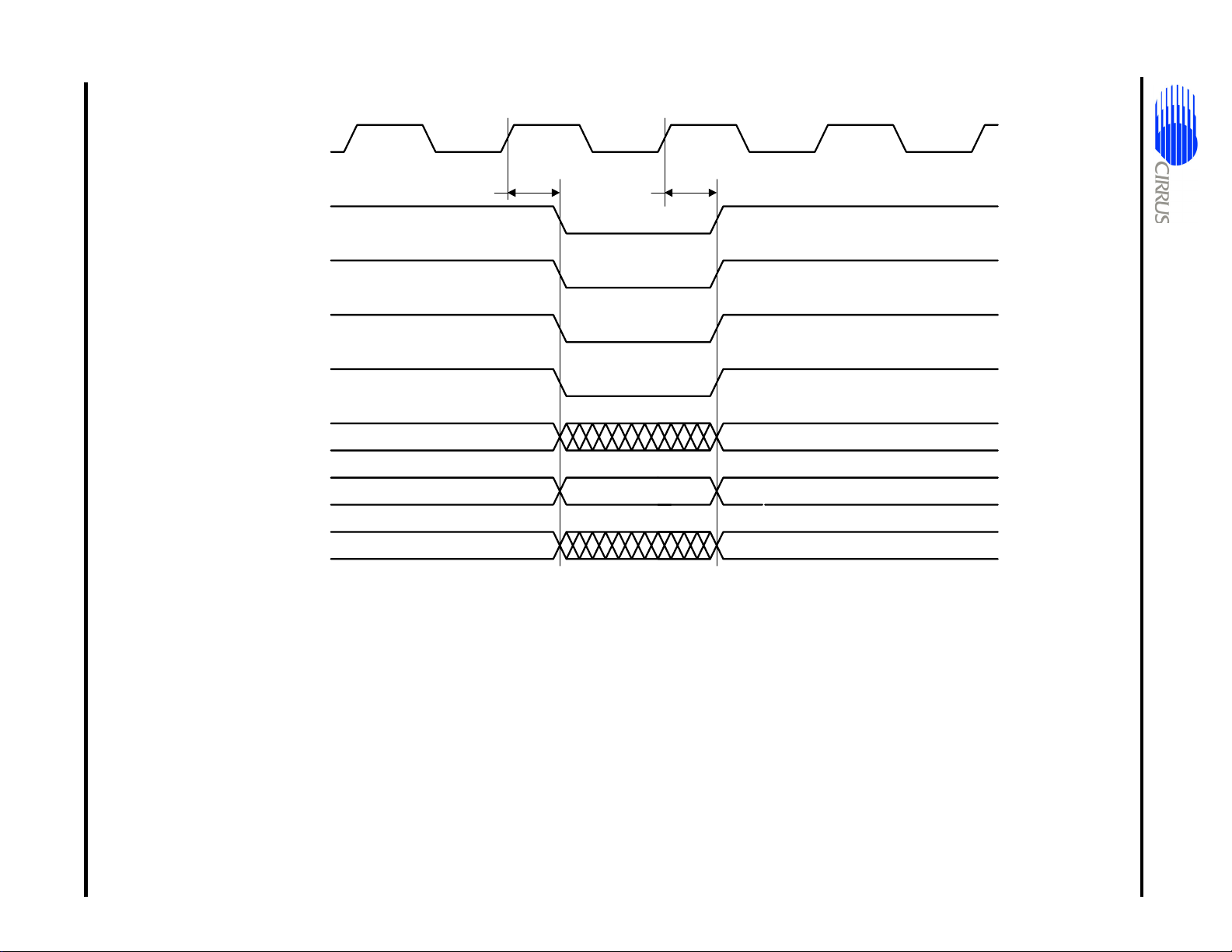
5.16 Switching Characteristics — SDRAM Interface
Refer to Figure 11 through Figure 14.
(SD_CLKOUT = SD_CLKIN)
Parameter Symbol Min Typical Max Unit
SD_CLKIN high time t
SD_CLKIN low time t
SD_CLKOUT rise/fall time t
sdclkh
sdclkl
sdclkrf
SD_CLKOUT Frequency 150 MHz
SD_CLKOUT duty cycle - 45 55 %
SD_CLKOUT rising edge to signal valid t
Signal hold from SD_CLKOUT rising edge t
SD_CLKOUT rising edge to SD_DQMn valid t
SD_DQMn hold from SD_CLK OUT ri sing edg e t
SD_DATA valid setup to SD_CLKIN rising edge t
SD_DATA valid hold to SD_CLKIN rising edge t
SD_CLKOUT rising edge to ADDRn valid t
sdcmdv
sdcmdh
sddqv
sddqh
sddsu
sddh
sdav
2.3 - ns
2.3 - ns
-1ns
-3.8ns
1.1 - ns
-3.8-ns
1.38 - ns
1.3 - ns
1.38 - ns
-3.8-ns
22 Copyright 2008 Cirrus Logic, Inc. DS868PP2
Page 23

DS868PP2 Copyright 2008 Cirrus Logic, Inc. 23
S
D_CLKOUT
SD_CS
SD_RAS
SD_CAS
SD_WE
SD_DQMn
SD_An
SD_Dn
SD_CLKIN
t
sdcmdv
t
sddqv
t
sdav
t
sdclkl
t
sdcmdh
CAS=2
t
sddsu
t
sdclkrf
00
t
sddh
LSP0 MSP0
LSP1 MSP1 LSP2 MSP2
t
sdclkh
t
sddqh
LSP3 MSP3
11
Figure 11. External Memory Interface - SDRAM Burst Read Cycle
32-bit Audio DSP Family
CS49DV8C Data Sheet
Page 24

DS868PP2 Copyright 2008 Cirrus Logic, Inc. 24
S
D_CLKOUT
SD_CS
SD_RAS
SD_CAS
SD_WE
SD_Dn
SD_An
SD_DQMn
t
sdcmdv
t
sdav
LSP0 MSP0 LSP1 MSP1 LSP2 MSP2 LSP3 MSP3
t
sddqv
t
sdcmdh
00 11
t
sddqh
Figure 12. External Memory Interface - SDRAM Burst Write Cycle
32-bit Audio DSP Family
CS49DV8C Data Sheet
Page 25

DS868PP2 Copyright 2008 Cirrus Logic, Inc. 25
S
D_CLKOUT
t
sdcmdv
t
sdcmdv
t
sdcmdh
SD_CS
SD_RAS
SD_CAS
SD_W E
SD_DQMn
SD_ADDRn
SD_DATAn
Figure 13. External Memory Interface - SDRAM Auto Refresh Cycle
32-bit Audio DSP Family
CS49DV8C Data Sheet
Page 26
DS868PP2 Copyright 2008 Cirrus Logic, Inc. 26
S
D_CLKOUT
t
sdcmdv
t
sdcmdh
SD_CS
SD_RAS
SD_CAS
SD_WE
SD_DQMn
SD_ADDRn
OPCODE
SD_DATAn
Figure 14. External Memory Interface - SDRAM Load Mode Register Cycle
32-bit Audio DSP Family
CS49DV8C Data Sheet
Page 27
CS49DV8C Data Sheet
32-bit Audio DSP Family
6. Ordering Infor mation
The CS49DV8C family part number is described as follows:
CS49DVNNI-XYZ
where
NN - Product Number Variant
I - ROM ID Number
X - Product Grade
Y - Package Type
Z - Lead (Pb) Free
Table 4. Ordering Information
Part No. Grade Temp. Range Container Package
CS49DV8C-CVZ Commercial 0 to +70 °C Tray
CS49DV8C-CVZR Commercial 0 to +70 °C Reel
7. Environmental, Manufacturing, and Handling Information
Table 5. Environmental, Manufacturing, and Handling Information
Model Number Peak Reflow Temp MSL Rating* Max Floor Life
CS49DV8C-CVZ 260 °C 3 7 Days
CS49DV8C-CVZR 260 °C 3 7 Days
* MSL (Moisture Sensitivity Level) as specified by IPC/JEDEC J-STD-020.
128-pin LQFP
27 Copyright 2008 Cirrus Logic, Inc. DS868PP2
Page 28

CS49DV8C Data Sheet
#
1
0
1
2
3
4
5
G
2
G
32-bit Audio DSP Family
8. Device Pin-Out Diagram
8.1 128-Pin LQFP Pin-Out Diagram
VDD6
GND6
GPIO37, SCP1_BSY#, PCP_BSY
VDDIO7
GNDIO7
VDD7
GND7
XTI
XTO
GNDA
VDD8
GND8
VDDIO8
GNDIO8
DBDA
DBCK
1
5
10
15
20
25
30
35
40
DAO_MCLK
GPIO19, DAO2_DATA1, HS4
GPIO38, PCP_WR# / DS#, SCP2_CLK
GPIO11, PCP_A3, AS#, SCP2_MISO / SDA
GPIO10, PCP_A2 / A10, SCP2_MOSI
GPIO8, PCP_IRQ#, SCP2_IRQ#
GPIO7, S CP1_CS#, IOWAIT
GPIO6, PCP_CS#, SCP2_CS#
GPIO14, DAI1_DATA3, TM3, DSD3
GPIO13, DAI1_DATA2, TM2, DSD2
GPIO12, DAI1_DATA1, TM1, DSD1
DAI1_DATA0, TM0, DSD0
PIO42, BDI_REQ# , DAI2_LRCLK, PCP_IRQ# / BSY#
GPIO43, BDI_CLK, DAI2_SCLK
BDI_DATA, DAI2_DATA, DSD5
GPIO26, DAO2_DATA3 / XMTB/UART_TX_EN
GPIO20, DAO2_DATA2, EE_CS#
GPOI9, SCP1_IRQ#
GPIO3, DDAC
GPIO2, UART_TXD
GPIO1, UART_RXD
GPIO0, UART_CLK
XTAL_OUT
PLL_REF_RES
VDDA (3.3V)
DAI1_SCLK, DSD-CLK
DAI1_LRCLK, DSD4
GPIO34, SCP1__MISO / SDA
GPIO33, SCP1_MOSI
GPIO35, SCP1_CLK
125
TEST
VDD1
GPIO22, DAO2_SCLK
GPIO18, DAO2_DATA0, HS3
VDDIO6
GNDIO6
EXT_CS1#
EXT_OE#
RESET#
120
128-Pin LQFP
45
GND1
GPIO23,
DAO2_LRCLK
GPIO16, DAO1_DATA2, HS2
GPIO15, DAO1_DATA1, HS1
PIO17, DAO1_DATA3 / XMTA
GND5
EXT_A18
EXT_A19
115
50
VDDIO1
DAO1_SCLK
DAO1_DATA0, HS0
VDD5
EXT_A16
EXT_A17
55
VDD2
GNDIO1
DAO1_LRCLK
EXT_A15
GND2
SD_CS#
110
SD_DQM0
SD_CAS#
SD_RAS#
SD_D7, EXT_D7
SD_D6, EXT_D6
GNDIO5
105
VDDIO2
SD_BA0, EXT_A13
SD_D3, EXT_D3
SD_A10, EXT_A10
100
95
90
85
80
75
70
65
SD_D2, EXT_D2
SD_A0, EXT_A0
SD_A1, EXT_A1
VDDIO5
SD_A2, EXT_A2
GND4
SD_A3, EXT_A3
SD_A4, EXT_A4
VDD4
EXT_CS2#
SD_A5, EXT_A5
GNDIO4
SD_A6, EXT_A6
SD_A7, EXT_A7
VDDIO4
SD_A8, EXT_A8
SD_A9, EXT_A9
GND3
SD_A11, EXT_A1
SD_A12, EXT_A1
VDD3
SD_CLKEN
SD_CLKIN
SD_CLKOUT
SD_DQM1
SD_D8, EXT_D8
SD_D9, EXT_D9
GNDIO3
SD_D10, EXT_D1
SD_D11, EXT_D1
VDDIO3
SD_D12, EXT_D1
SD_D13, EXT_D1
SD_D14, EXT_D1
SD_D15, EXT_D1
SD_D0, EXT_D0
GNDIO2
EXT_WE#
SD_D1, EXT_D1
SD_WE#
SD_BA1, EXT_A14
60
SD_D5, EXT_D5
SD_D4, EXT_D4
Figure 15. 128-Pin LQFP Pin-Out
28 Copyright 2008 Cirrus Logic, Inc. DS868PP2
Page 29
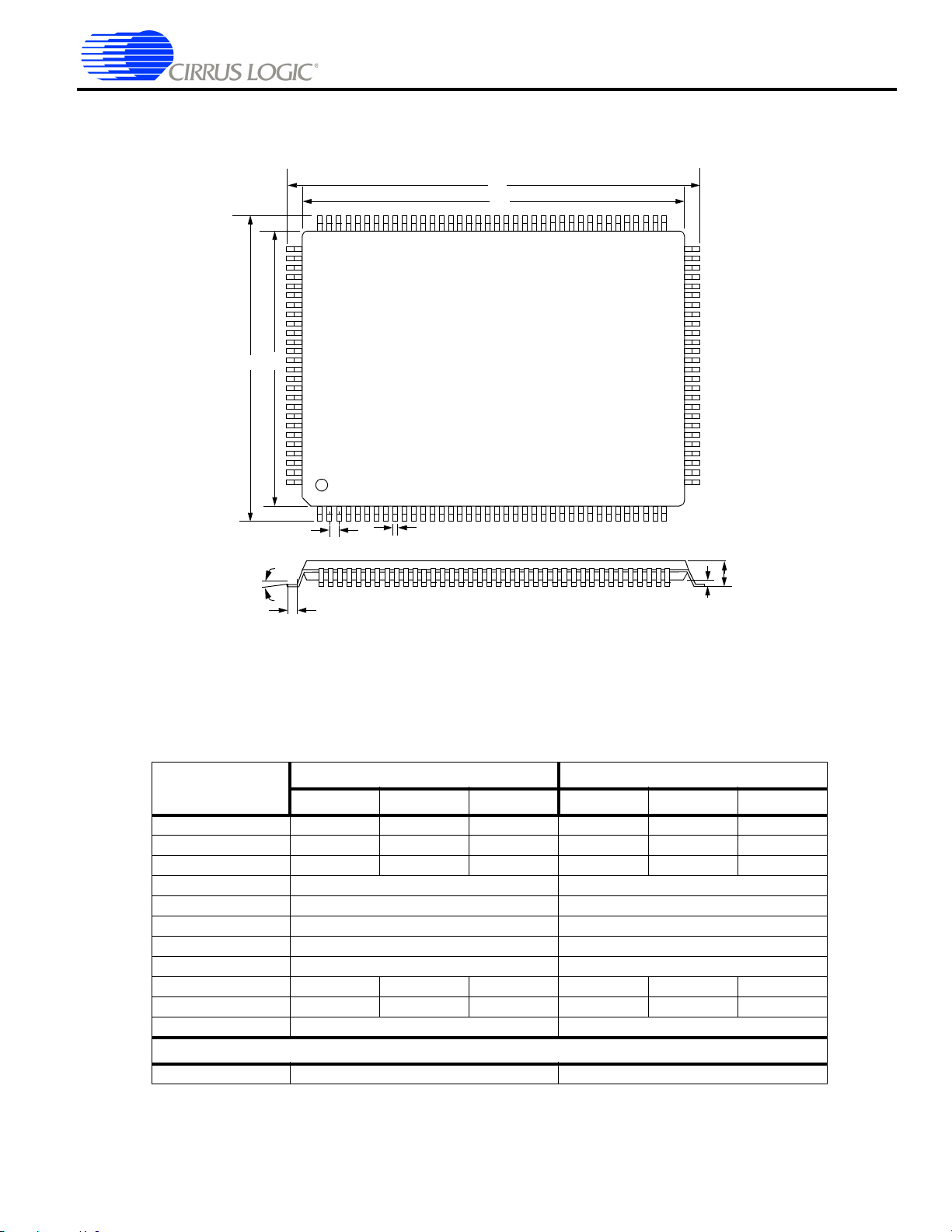
9. Package Mechanical Drawings
9.1 128-Pin LQFP Package
E1
E
1
CS49DV8C Data Sheet
32-bit Audio DSP Family
D
D1
e
∝
L
b
A
A1
Figure 16. 128-Pin LQFP Package Drawing
T able 6. 128-Pin LQFP Package Characteristics
DIM
MIN NOM MAX MIN NOM MAX
A --- --- 1.60 --- --- .063”
A1 0.05 --- 0.15 .002” --- .006”
b 0.17 0.22 0.27 .007” .009” .011”
D 22.00 BSC .866”
D1 20.00 BSC .787”
E 16.00 BSC .630”
E1 14.00 BSC .551”
e 0.50 BSC .020”
q 0° 3.5 7° 0° 3.5 7°
L 0.45 0.60 0.75 .018” .024” .030”
L1 1.00 REF .039” REF
ddd 0.08 .003”
MILLIMETERS INCHES
TOLERANCES OF FORM AND POSITION
DS868PP2 Copyright 2008 Cirrus Logic, Inc. 29
Page 30
CS49DV8C Data Sheet
32-bit Audio DSP Family
10. Revision History
Revision Date Changes
PP1 September 2, 2008 Initial Release.
PP2 September 25, 2008 Removed references to External Parallel Flash / SRAM Interface.
30 Copyright 2008 Cirrus Logic, Inc. DS868PP2
 Loading...