

Page 1
CS4970x4 Data Sheet
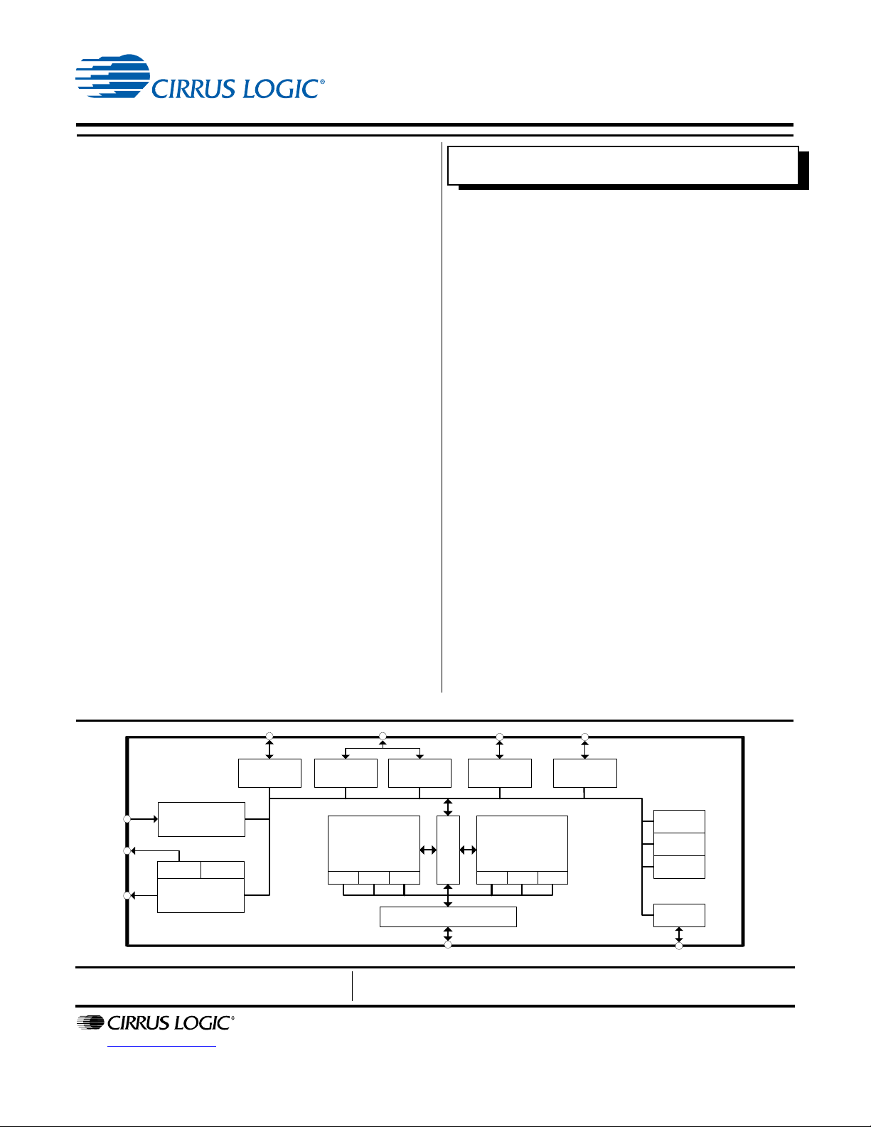
Coyote 32-bit
DSP A
D
M
A
Coyote 32-bit
DSP B
Ext. Memory Controller
P
S/PDIF
X Y P X Y
Serial
Control 1
16 Ch PCM
Audio Out
Serial
Control 2
Parallel
Control
GPIO Debug
STC
TMR1
TMR2
PLL
S/PDIF
12 Ch. Audio In /
6 Ch. SA CD In
FEATURES
Multi-standard 32-bit high-definition audio decoding plus
post-processing
Supports high-definition audio formats including:
®
— Dolby Digital
— Dolby
®
—DTS-HD
—DTS-HD
— DTS Express™ 5.1
Supports legacy audio formats and a wide array of post-
processing
— Dolby Digital® EX, Dolby Pro Logic® II, IIx, IIz 7.1, Dolby
Headphone® 2, Dolby Virtual Speaker® 2, Dolby
Volume® (original), Dolby Volume 258 (lite), Audistry
— DTS-ES 96/24™ Discrete 7.1, DTS-ES™ Discrete 7.1,
DTS-ES™ Matrix 6.1, DTS Neo:6®, DTS Neural
Surround
— MPEG-2 AAC
®
—SRS
Circle Surround® II, SRS Circle Surround Auto,
SRS Circle Surround Decoder Optimized, SRS
TruVolume™ 7.1 (V 2.1.0.0), SRS TruSurround
HD/HD4®, SRS WOW HD™, SRS CS Headphone™,
SRS Circle Cinema 3D
—THX® Ultra2™, THX Select2
Cirrus Logic’s Applications Library
— Cirrus Original Multi-Channel Surround 2 (COMS2),
Cirrus Band XpandeR
Technology (CVT), Cirrus Intelligent Room Calibration 2
(IRC2), Cirrus Bass Enhancement (CBE)
— Crossbar Mixer, Signal Generator
— Advanced Post-Processors including: 7.1 Bass Manager
Quadruple Crossover, Tone Control, 11- Band
Parametric EQ, Delay, 2:1/4:1 Decimator, 1:2/1:4
Upsampler
Plus
TrueHD
®
High Resolution Audio
Master Audio
™
DTS Surround Sensation Speaker
™
LC 5.1
™
™
, SRS Studio Sound HD
™
™
, Cirrus Virtualization
™
High Definition Audio Decoder DSP Family
with Dual 32-bit Engine Technology
Up to 12 Channels of 32-bit Serial Audio Input
Customer Software Security Keys
16 Ch x 32-bit PCM Out with Dual 192 kHz S/PDIF Tx
Two SPI
™/I2C™
ports
Large On-chip X, Y, and Program RAM & ROM
SDRAM and Serial Flash Memory Support
The CS4970x4 DSP family is an enhanced version of the
CS4953xx DSP family with higher overall performance. In
®
addition to all the mainstream audio processing codes in onchip ROM that the CS4953xx DSP offers, the CS4970x4 device
family also supports the decoding of major high-definition audio
formats. Additionally, the CS4970x4, a dual-core device,
performs the high-definition audio decoding on the first core,
leaving the second core available for audio post-processing and
audio enhancement. The CS4970x4 device supports the most
demanding audio post processing requirements. It provides an
easy upgrade path to systems currently using the CS495xx or
CS4953xx device with minor (or no) hardware and software
changes.
Ordering Information
See page 27 for ordering information.
Preliminary Product Information
http://www.cirrus.com
This document contains information for a new product.
Cirrus Logic reserves the right to modify this product without notice.
Copyright © 2014 Cirrus Logic, Inc. FEB 2014
All Rights Reserved DS752F1
Page 2
CS4970x4 Data Sheet
32-bit High Definition Audio Decoder DSP Family
Table of Contents
1 Documentation Strategy .................................... ................................. ................. ................ ......4
2 Overview .....................................................................................................................................4
2.1 Migrating from CS495xx(3) to CS4970x4 .................................................................................................5
2.2 Licensing ............................ .... ....................................................... ...........................................................5
3 Code Overlays ............................................................................................................... .............5
4 Hardware Functional Description ............................................................................................6
4.1 Coyote DSP Core ............................................ .... ... ... ... .... ... .....................................................................6
4.1.1 DSP Memory ................... ... .... ... ....................................................... ... ... ... .... ... ... ... .....................6
4.1.2 DMA Controller ...... .... ... ....................................................... ... ... ... .... ... ... ... ..................................7
4.2 On-chip DSP Peripherals .........................................................................................................................7
4.2.1 Digital Audio Input Port (DAI) .......................................................................................................7
4.2.2 Digital Audio Output Port (DAO) ..................................................................................................7
4.2.3 Serial Control Port 1 & 2 (I
4.2.4 External Memory Interface ..................................... ... ... .... ... ... ... ... .... ...........................................7
4.2.5 General Purpose Input/Output (GPIO) ........................................................................................7
4.2.6 Phase-locked Loop (PLL)-based Clock Generator ....... ....................................................... ........7
4.3 DSP I/O Description .................................................................................................................................8
4.3.1 Multiplexed Pins ................................. .... ... ....................................................... ... ... .....................8
4.3.2 Termination Requirements ...........................................................................................................8
4.3.3 Pads ................................ ... .... ... ... ... ....................................................... .....................................8
4.4 Application Code Security ........................................................................................................................8
2
C or SPI) ..........................................................................................7
5 Characteristics and Specifications ..........................................................................................8
5.1 Absolute Maximum Ratings ......................................................................................................................8
5.2 Recommended Operating Conditions ......................................................................................................9
5.3 Digital DC Characteristics ........................................................................................................................9
5.4 Power Supply Characteristics .......................................... ... ... ... ...............................................................9
5.5 Thermal Data (128-pin LQFP) ................................................ ................................................................10
5.6 Switching Characteristics—
5.7 Switching Characteristics — XTI .................. ....................................................................... ................... 11
5.8 Switching Characteristics — Internal Clock ............................................................................................12
5.9 Switching Characteristics — Serial Control Port - SPI Slave Mode .......................................................13
5.10 Switching Characteristics — Serial Control Port - SPI Master Mode ...................................................14
5.11 Switching Characteristics — Serial Control Port - I
5.12 Switching Characteristics — Serial Control Port - I
5.13 Switching Characteristics — Parallel Control Port - Intel Slave Mode ........................ ... ......................16
5.14 Switching Characteristics — Parallel Control Port - Motorola Slave Mode .........................................19
5.15 Switching Characteristics — Digital Audio Slave Input Port .................................................................21
5.16 Switching Characteristics — Digital Audio Output Port ........................................................................22
5.17 Switching Characteristics — SDRAM Interface ....................................................................................23
RESET ...................................... ............................................. ...................... 11
2
C Slave Mode ... ... ................................................15
2
C Master Mode ....................................................16
6 Ordering Information ...............................................................................................................27
7 Environmental, Manufacturing, and Handling Information .................................................27
8 Device Pin-Out Diagram ..........................................................................................................28
8.1 128-Pin LQFP Pin-Out Diagram .............................................................................................................28
9 Package Mechanical Drawings ...............................................................................................29
9.1 128-Pin LQFP Package Drawing ...........................................................................................................29
10 Revision History .....................................................................................................................30
DS752F1 2
Page 3

CS4970x4 Data Sheet
32-bit High Definition Audio Decoder DSP Family
List of Figures
Figure 1. RESET Timing .........................................................................................................................................11
Figure 2. XTI Timing ..............................................................................................................................................11
Figure 3. Serial Control Port - SPI Slave Mode Timing ..........................................................................................13
Figure 4. Serial Control Port - SPI Master Mode Timing ........................................................................................14
Figure 5. Serial Control Port - I
Figure 6. Serial Control Port - I
Figure 7. Parallel Control Port - IntelÒ Slave Mode Read Cycle ........................................... .... ... ... ... ... .... ............17
Figure 8. Parallel Control Port - Intel Slave Mode Write Cycle ..............................................................................18
Figure 9. Parallel Control Port - MotorolaÒ Slave Mode Read Cycle Timing ........................................................20
Figure 10. Parallel Control Port - Motorola Slave Mode Write Cycle Timing .........................................................20
Figure 11. Digital Audio Input (DAI) Port Timing Diagram .....................................................................................21
Figure 12. DAI Slave Timing Diagram ...................................................................................................................21
Figure 13. Digital Audio Port Output Timing Master Mode .....................................................................................22
Figure 14. Digital Audio Output Timing, Slave Mode (Relationship LRCLK to SCLK) ............... ... ... ... ... .... ... ... ... ...23
Figure 15. External Memory Interface - SDRAM Burst Read Cycle .......................................................................24
Figure 16. External Memory Interface - SDRAM Burst Write Cycle .......................................................................24
Figure 17. External Memory Interface - SDRAM Auto Refresh Cycle ....... .... ... ... ... ... .... ... ......................................25
Figure 18. External Memory Interface - SDRAM Load Mode Register Cycle ........................................................26
Figure 19. 128-Pin LQFP Pin-Out Diagram ...........................................................................................................28
Figure 20. 128-Pin LQFP Package Drawing ..........................................................................................................29
2
C Slave Mode Timing ..........................................................................................15
2
C Master Mode Timing .............. .... ... ... ... .... ... ......................................................16
List of Tables
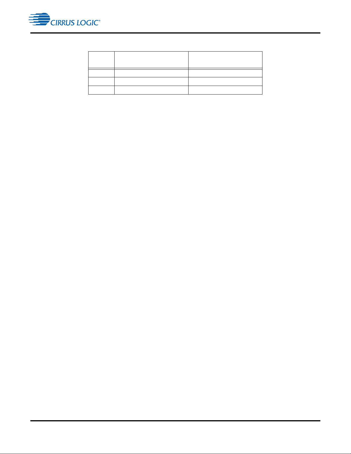
Table 1. CS4970x4 Related Documentation . . . . . . . . . . . . . . . . . . . . . . . . . . . . . . . . . . . . . . . . . . . . . . . . . . . . . . 4
Table 2. Device and Firmware Selection Guide. . . . . . . . . . . . . . . . . . . . . . . . . . . . . . . . . . . . . . . . . . . . . . . . . . . . 5
Table 3. CS4970x4 DSP Memory Sizes . . . . . . . . . . . . . . . . . . . . . . . . . . . . . . . . . . . . . . . . . . . . . . . . . . . . . . . . . 7
Table 4. Ordering Information . . . . . . . . . . . . . . . . . . . . . . . . . . . . . . . . . . . . . . . . . . . . . . . . . . . . . . . . . . . . . . . . 27
Table 5. Environmental, Manufacturing, & Handling Information. . . . . . . . . . . . . . . . . . . . . . . . . . . . . . . . . . . . . . 27
Table 6. 128-Pin LQFP Package Characteristics . . . . . . . . . . . . . . . . . . . . . . . . . . . . . . . . . . . . . . . . . . . . . . . . . 29
DS752F1 3
Page 4
CS4970x4 Data Sheet
32-bit High Definition Audio Decoder DSP Family
1 Documentation Strategy
The CS4970x4 data sheet describes the CS4970x4 family of multichannel audio decoders. This document
should be used in conjunction with the following documents when evaluating or designing a system around the
CS4970x4 family of processors.
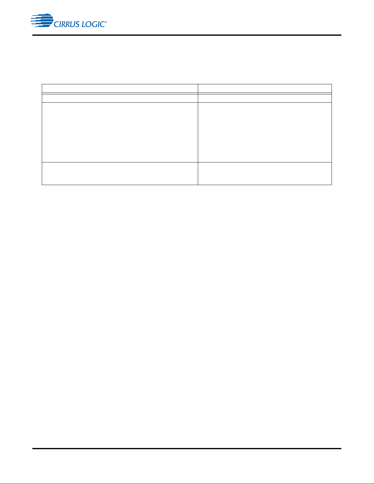
Table 1. CS4970x4 Related Documentation
Document Name Description
CS4970x4 Data Sheet This document
A new consolidated documentation set that includes:
• Detailed system design information including
Typical Connection Diagrams, Boot-Procedures,
CS495314/CS4970x4 System Designer’s Guide
AN288 - CS4953xx/CS4970x4 Firmware User’s Manual
Pin Descriptions, Etc. Also describes use of DSP
Condenser tool.
• Detailed firmware design information including
signal processing flow diagrams and control API
information
Includes detailed firmware design information
including signal processing flow diagrams and control
API information
The scope of the CS4970x4 data sheet is primarily to provide hardware specifications of the CS4970x4 family
of devices. This includes hardware functionality, characteristic data, pinout, and packaging information.
The intended audience for the CS4970x4 data sheet is the system PCB designer, MCU programmer, and the
quality control engineer.
2 Overview
The CS4970x4 DSP Family, combined with Cirrus Logic’s comprehensive library of audio processing
algorithms, enables the development of next-generation high-definition audio solutions. Cirrus Logic also
provides a broad array of digital interface products and audio converters to meet your audio system-level
design requirements.
Note: The CS4970x4 is available in a 128-pin LQFP package.
The audio processing features of the CS4970x4 product family are a superset of audio features available in
the CS4953xx product family.
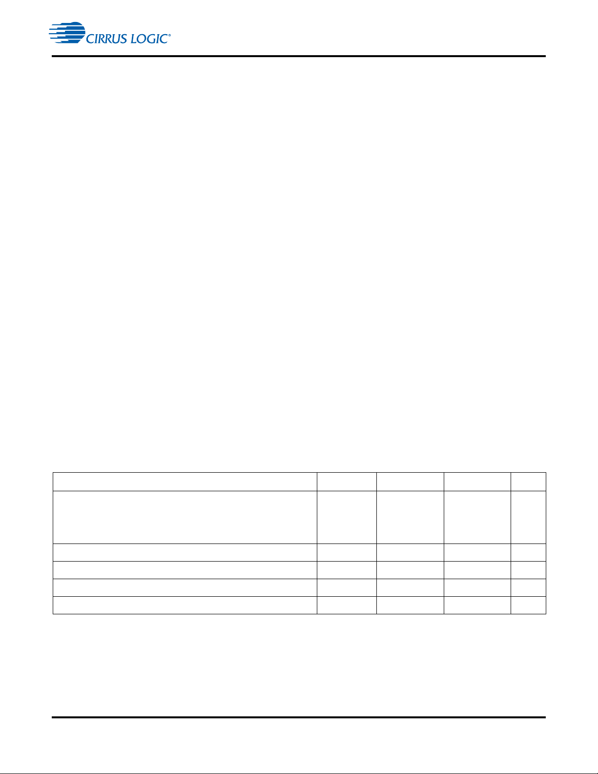
Refer to Table 2 on page 5 for the speed and firmware features of the CS4970x4 product family.
DS752F1 4
Page 5
32-bit High Definition Audio Decoder DSP Family
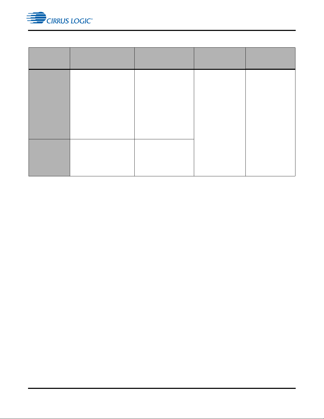
Table 2. Device and Firmware Selection Guide
CS4970x4 Data Sheet
Device
CS497014
300MACS
CS497004
300MACS
CS497024
300MACS
1. Additional processing (MPMA, MPMB/VPM, PPM) post any of the HD audio decoders may be limited. Contact your Cirrus Logic
FAE for the latest concurrency matrix.
2. Downsampling and Upsampling functionality is located in the operating system. The Cirrus Decimator (Down-Sampler) is also
available as a separate post-processing module that is described in the application note AN288PPI.
3. The indicated HD audio decoder algorithms require external SDRAM. Consult your Cirrus Logic FAE for the recommended
SDRAM size for your design.
Decode Processor
(DSP-A)
Stereo PCM
(4:1/2:1 Down-sampling and
1:2/1:4 U-sampling Options)
Multichannel PCM
(4:1/2:1 Down-sampling and
1:2/1:4 Up-sampling Options)
Dolby Digital
MPEG-2 AAC LC 5.1
Dolby Digital Plus
Dolby TrueHD
Same as CS497014 +
DTS, DTS-ES, DTS96/24
DTS-HD Master Audio
DTS-HD High Res Audio
DTS Express 5.1
1
3
Matrix Processor Module
(DSP-A)
Dolby Pro Logic II / IIx / IIz 7.1
SRS Circle Surround II / Circle
2
Surround Auto / Circle
Surround Decoder Optimized
(Stereo In)
2
Cirrus Original Multi-Channel
Surround 2 (Effects / Reverb
Processor)
Crossbar (Down-mix / Up-mix)
(Simultaneous Process)
3
3
Same as CS497014 +
DTS Neo:6, DTS Neural
Surround
1
Virtualizer Processor
Module
(DSP-B)
Cirrus Virtualizer
Technology
Dolby Headphone 2
Dolby Virtual Speaker 2
SRS CS Headphone
SRS TruSurround HD/HD4
1
Post Processor
Module
(DSP-B)
APP
(Advanced Postprocessing)
–Tone Control
–Select 2
–PEQ (up to 11 Bands)
–Delay
(Speaker to Listening
Position Alignment
and/or Lip Sync)
–7.1 Bass Manager
–Audio Manager
–4:1/2:1 Down-sampling
SRS TruVolume 7.1
Multichannel
Dolby Volume
Multichannel
1
2
2.1 Migrating from CS495xx(3) to CS4970x4
CS4970x4 was designed to provide an easy upgrade path from the CS495xx and CS4953x. There are some
small differences the hardware designer should be aware of:
• The PLL supply voltage on the CS4970x4 is 3.3V vs. 1.8V on the CS495xx.
• The PLL filter topology is simpler when using the CS4970x4 rather than the CS495xx.
• The CS4970x4 adds support for Time-division multiplexing (TDM) mode on both audio input and output
ports.
• The CS4970x4 does not support external static random access memory (SRAM) operation.
• The CS4970x4 external Synchronous dynamic random access memory (SDRAM) bus speed is fixed at
150 MHz vs. the 120 MHz maximum bus speed for the CS495xx. Some firmware modules also support a
75 MHz CS4970x4 SDRAM bus speed. Refer to AN304 for details.
• The CS4970x4 CLKOUT pin can output XTALI or XTALI/2. The CS495xx can only output XTALI.
2.2 Licensing
Licenses are required for all of the third party audio decoding/processing algorithms listed below, including the
application notes. Contact your local Cirrus Sales representative for more information.
3 Code Overlays
The suite of software available for the CS4970x4 family consists of operating systems (OS) and a library of
overlays. The overlays have been divided into three main groups: decoders, matrix processors, and
postprocessors. All software components are defined in the following list:
DS752F1 5
Page 6

CS4970x4 Data Sheet
32-bit High Definition Audio Decoder DSP Family
• OS/Kernel - Encompasses all non-audio processing tasks, including loading data from external memory,
processing host messages, calling audi o- pr oc es sin g subroutines, auto-detection, error concealment, etc.
• Decoders - Any module that initially writes data into the audio I/O buf fers, e.g. AC-3
the decoding/processing algorithms listed require delivery of PCM or IEC61937-packed, compressed data
2
via I
S- or LJ-formatted digital audio to the CS4970x4 from A/D converters, SPDIF Rx, HDMI Rx, etc.
™
, DTS, PCM, etc. All
• Matrix-processors - Any module that processes audio I/O buffer PCM data in-place before the Postprocessors. Generally speaking, these modules alter the number of valid channels in the audio I/O buffer
through processes like Virtualization (n2 channels) or Matrix Decoding (2n channels). Examples are
Dolby ProLogic IIx and DTS Neo:6.
• Virtualizer-processor - Any module that encodes PCM data into fewer output channels than input
channels (n2 channels) with the effect of providing “phantom” speakers to represent the physical audio
channels that were eliminated. Examples are Dolby Headphone 2 an d Dolby V irtual Speaker 2. Generally
speaking, these modules reduce the number of valid channels in the audio I/O buffer.
• Post-processors - Any module that processes audio I/O buffer PCM data in-place after the matrix
processors. Examples are bass management, audio manager, tone control, EQ, delay, customer-specific
effects, Dolby Headphone/Virtual Speaker, etc.
The overlay structure reduces the time required to reconfigure the DSP when a processing change is
requested. Each overlay ca n be reloaded independently without disturbing the other overlays. For example,
when a new decoder is selected, the OS, matrix-, and post-processors do not need to be reloaded — only the
new decoder (the same is true for the other overlays).
4 Hardware Functional Description
4.1 Coyote DSP Core
The CS4970x4 is a dual-core Coyote DSP with separate X and Y data and P code memory spaces. Each core
is a high-performance, 32-bit, user-programmable, fixed-point DSP that is capable of performing two multiply
accumulate (MAC) operations per clock cycle. Each core has eight 72-bit accumu lators, four X- and four Y-data
registers, and 12 index registers.
Both DSP cores are coupled to a flexible DMA engine. The DMA engine can move data between peripherals
such as the digital audio input (DAI) and digital audio output (DAO), external memory, or any DSP core
memory , all with out the intervention of the DSP. The DMA engine of floads dat a move instructio ns from the DSP
core, leaving more MIPS available for signal processing instructions.
CS4970x4 functionality is controlled by application codes that are stored in on-board ROM or downloaded to
the CS4970x4 from a host MCU or external FLASH/EEPROM. Users can choose to use standard audio
decoder and post-processor modules which are available from Cirrus Logic.
The CS4970x4 is suitable for audio decoder, audio post-processor, audio encoder, DVD audio/video player,
and digital broadcast decoder applications.
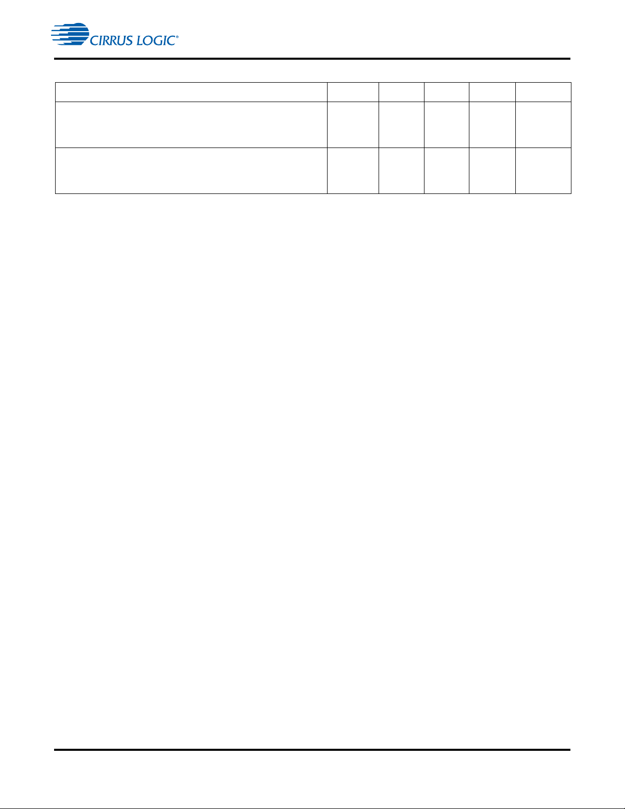
4.1.1 DSP Memory
Each DSP core has its own on-chip data and progra m RAM and ROM and does not require external memory
for any of today’s popular audio algorithms including Dolby Digital Surround EX, AAC Multichannel, DTS-ES
96/24, and THX Ultra2. However, if the end-system design requires support of the new high-definition audio
formats, external SDRAM will be needed to support Dolby TrueHD and DTS-HD master audio.
The memory maps for the DSPs are as follows. All memory sizes are composed of 32-bit words.
DS752F1 6
Page 7
32-bit High Definition Audio Decoder DSP Family
Table 3. CS4970x4 DSP Memory Sizes
CS4970x4 Data Sheet
Memory
Type
X 16K SRAM, 32K ROM 10K SRAM, 8K ROM
Y 24K SRAM, 32K ROM 16K SRAM, 16K ROM
P 8K SRAM, 32K ROM 8K SRAM, 24K ROM
DSP A DSP B
4.1.2 DMA Controller
The powerful 12-channel DMA controller can move data between 8 on-chip resources. Each resource has its
own arbiter: X, Y, and P RAM/ROMs on DSP A; X, Y, and P RAM/ROMs on DSP B; external memory; and the
peripheral bus. Modulo and linear addressing modes are supported, with flexible start address and increment
controls. The service interval for each DMA channel as well as up to 6 interrupt events, is programmabl e.
4.2 On-chip DSP Peripherals
4.2.1 Digital Audio Input Port (DAI)
The 12-channel (6-line) DAI port support s a wide vari ety of dat a input forma t s. The port is capable of accepting
PCM or IEC61937. Up to 32-bit word lengths are supported. Additionally, support is provided for audio data
input to the DSP via the DAI from an HDMI receiver.
The port has two independent slave-only clock domains. Each data input can be independently assigned to a
clock domain. The sample rate of the input clock domains can be determined automatically by the DSP, which
off-loads the task of monitorin g the SPDIF rece iver from the host. A time -stam ping feature allows the input dat a
to be sample-rate converted via software.
4.2.2 Digital Audio Output Port (DAO)
There are two DAO ports. Each port can output 8 channels of up to 32-bit PCM data. The port supports data
rates from 32 kHz to 192 kHz. Each port can be configured as an independent clock domain in slave mode, or
the ratio of the two clocks can be set to even multiples of each other in master mode. The two por ts can also b e
ganged together into a single clock domain. Each port has one serial audio pin that can be configured as a
192-kHz SPDIF transmitter (data with embedded clock on a single line).
4.2.3 Serial Control Port 1 & 2 (I
2
C or SPI)
There are two on-chip serial contro l ports that are capable of operating as master or slave in either I
modes. SCP1 defaults to slave operation. It is dedicated for external host-control and supports an external
clock up to 50 MHz in SPI mode. This high clock speed enables very fast code download, control or data
delivery. SCP2 defaults to master mode and is dedicated for booting from external serial Flash memory or for
audio sub-system control.
4.2.4 External Memory Interface
The external memory interface controller supports up to 128 Mbits of SDRAM, using a 16-bit data bus.
4.2.5 General Purpose Input/Output (GPIO)
Many of the CS4970x4 peripheral pins are multiplexed with GPIO. Each GPIO can be configured as an output,
an input, or an input with interrupt. Each input-pin interrupt can be configured as rising edge, falling edge,
active-low, or active-high.
4.2.6 Phase-locked Loop (PLL)-based Clock Generator
The low-jitter PLL generates integer or fractional multiples of a reference frequency which are used to clo ck the
DSP core and peripherals. Through a second PLL divider chain, a dependent clock domain can be output on
the DAO port for driving audio converters. The CS4970x4 defaults to running from the external reference
frequency and can be switched to use the PLL output after overlays have been loaded and configured, either
2
C or SPI
DS752F1 7
Page 8
CS4970x4 Data Sheet
32-bit High Definition Audio Decoder DSP Family
through master boot from an external FLASH or through host control. A built-in crystal oscillator circuit with a
buffered output is provided. The buffered output frequency ratio is selectable between 1:1 (default) or 2:1.
4.3 DSP I/O Description
4.3.1 Multiplexed Pins
Many of the CS4970x4 pins are multi-functional. For details on pin functionality please refer to the CS4970x4
System Designer’s Guide.
4.3.2 Termination Requirements
Open-drain pins on the CS4970x4 must be pulled high for proper operation. Please refer to the CS4970x4
System Designer’s Guide to identify which pins are open-drain and what value of pull-up resistor is require d for
proper operation.
Mode select pins on the CS4970x4 are used to select the boot mode upon the rising edge of reset. A detailed
explanation of termination requirements for each communication mode select pin can be found in the
CS4970x4 System Designer’s Guide.
4.3.3 Pads
The CS4970x4 I/O operates from the 3.3 V supply and is tolerant within 5 V.
4.4 Application Code Security
The external program code may be encrypted by the programmer to protect any intellectual property it may
contain. A secret, customer-specific key is used to encrypt the program code that is to be stored external to the
device.
5 Characteristics and Specifications
Note: All data sheet minimum and maximum timing parameters are guaranteed over the rated voltage
and temperature. All data sheet typical parameters are measured under the following conditions:
T=25°C, C
5.1 Absolute Maximum Ratings
(GNDD = GNDIO = GNDA = 0 V; all voltages with respect to 0 V)
DC power supplies: Core supply
Input pin current, any pin except supplies
Input voltage on PLL_REF_RES
Input voltage on I/O pins
Storage temperature
CAUTION: Operation at or beyond these limits may result in permanent damage to the de vice. Normal oper ation is
not guaranteed at these extremes.
= 20 pF, VDD = 1.8 V, VDDA = VDDIO = 3.3 V, GNDD = GNDIO = GNDA = 0 V.
L
Parameter Symbol Min Max Unit
V
V
V
V
PLL supply
I/O supply
|VDDA – VDDIO|
VDD
VDDA
VDDIO
I
in
V
filt
V
inio
T
stg
–0.3
–0.3
–0.3
—
2.0
3.6
3.6
0.3
—+/- 10mA
-0.3 3.6 V
-0.3 5.0 V
-65 150 °C
DS752F1 8
Page 9

5.2 Recommended Operating Conditions
(GNDD = GNDIO = GNDA = 0 V; all voltages with respect to 0 V)
Parameter Symbol Min Typ Max Unit
DC power supplies: Core supply
PLL supply
I/O supply
|VDDA – VDDIO|
Ambient operating temperature
Commercial Grade (CQZ/CVZ)
CS4970x4 Data Sheet
32-bit High Definition Audio Decoder DSP Family
VDD
VDDA
VDDIO
1.71
3.13
3.13
1.8
3.3
3.3
1.89
3.46
3.46
0
T
A
0 +25 + 70
V
V
V
V
°C
Commercial
T
j
0+125ºC
Note: It is recommended that the 3.3 V IO supply come up ahead of or simultaneously with the 1.8 V core supply.
5.3 Digital DC Characteristics
(Measurements performed under static conditions.)
Parameter Symbol Min Typ Max Unit
High-level input voltage
Low-level input voltage, except XTI
Low-level input voltage, XTI
Input Hysteresis
High-level output voltage (IO = -4mA), except XTI, SDRAM
pins
Low-level output voltage (IO = 4mA), except XTI, SDRAM
pins
SDRAM High-level output voltage (IO = -8mA)
SDRAM Low-level output voltage (IO = 8mA)
Input leakage current (all digital pins with internal pull-up
resistors disabled)
Input leakage current (all digital pins with internal pull-up
resistors enabled, and XTI)
V
V
V
ILXTI
V
hys
V
OH
V
V
OH
V
I
IN
I
IN-PU
IH
IL
OL
OL
2.0 — — V
——0.8 V
——0.6 V
—0.4— V
VDDIO * 0.9 — — V
——VDDIO * 0.1V
VDDIO * 0.9 — — V
——VDDIO * 0.1V
—— 5 A
——70 A
5.4 Power Supply Characteristics
(Measurements performed under operating conditions.)
Parameter Min Typ Max Unit
Power supply current:
Core and I/O operating: VDD
PLL operating: VDDA
With external memory and most ports operating: VDDIO
1.Dependent on application firmware and DSP clock speed.
1
—
—
—
350
3.5
120
—
—
—
mA
mA
mA
DS752F1 9
Page 10
5.5 Thermal Data (128-pin LQFP)
Parameter Symbol Min Typ Max Unit
CS4970x4 Data Sheet
32-bit High Definition Audio Decoder DSP Family
Thermal Resistance (Junction to Ambient)
Two-layer Board
Four-layer Board
Thermal Resistance (Junction to Top of Package )
Two-layer Board
Four-layer Board
ja
jt
—
—
—
—
53
44
.45
.39
—
—
—
—
1
2
1
2
°C / Watt
°C / Watt
Notes: 1. Two-layer board is specified as a 76 mm X 114 mm, 1.6 mm thick FR-4 material with 1-oz. copper covering 20% of the top and
bottom layers.
2. Four-layer board is specified as a 76 mm X 114 mm, 1.6 mm thick FR-4 material with 1-oz. copper covering 20% of the top and
bottom layers and 0.5-oz. copper covering 90% of the internal power plane and ground plane layers.
3. To calculate the die temperature for a given power dissipation
= Ambient Temperature + [ (Power Dissipation in Watts) * ja ]
j
4. To calculate the case temperature for a given power dissipation
= j - [ (Power Dissipation in Watts) * jt
c
DS752F1 10
Page 11

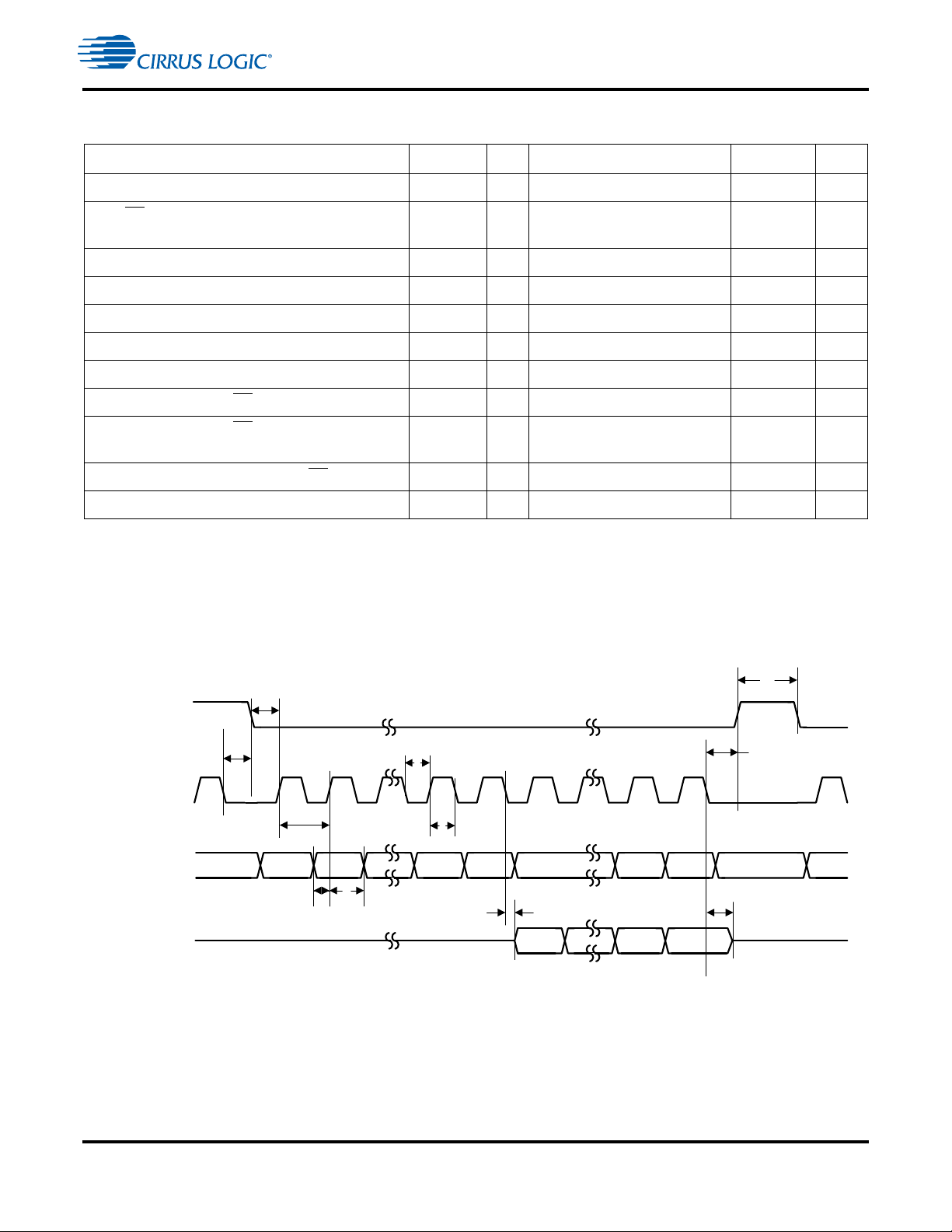
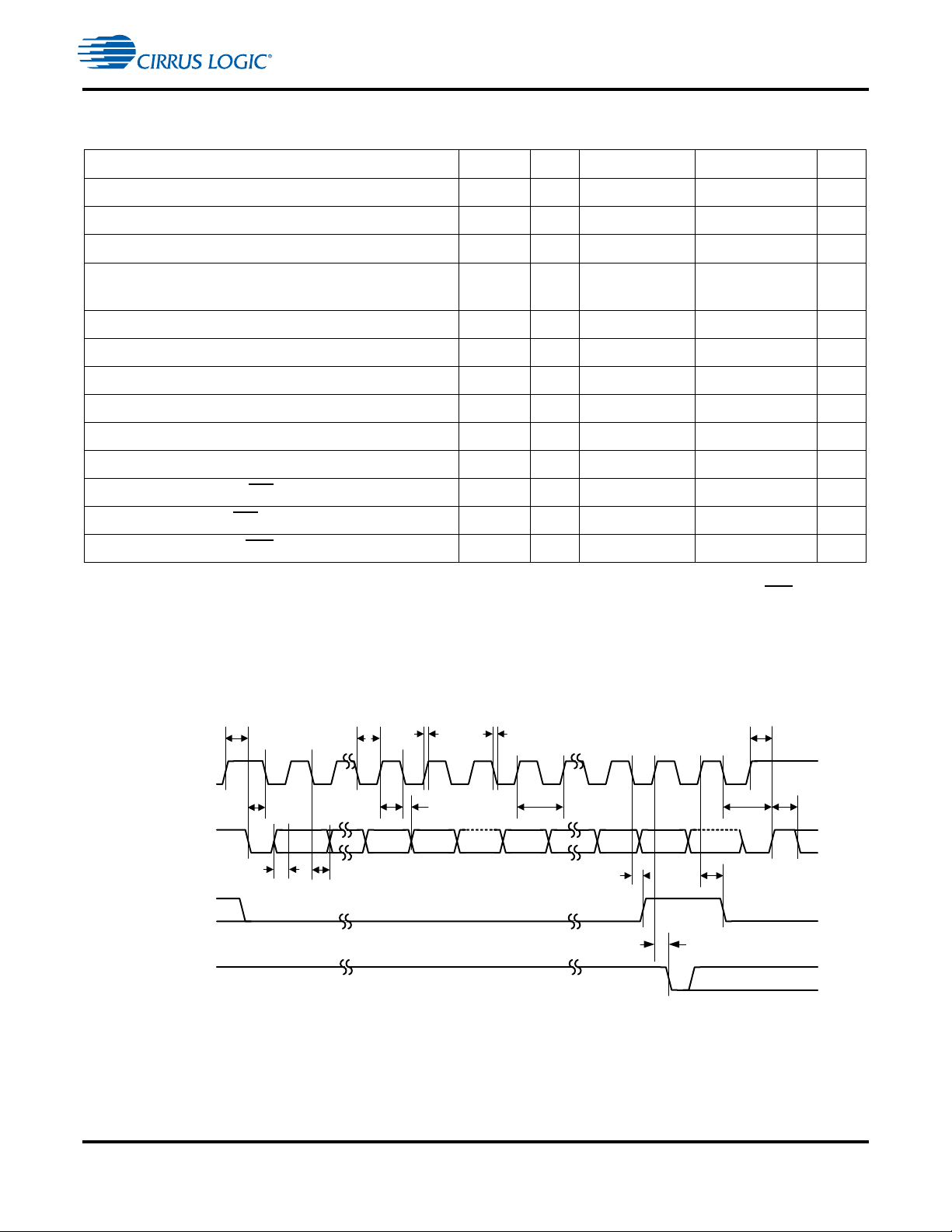
5.6 Switching Characteristics—RESET
RESET#
T
rst2z
T
rstl
T
rstsu
T
rsthld
HS[3:0]
All Bidirectional
Pins
t
clkih
t
clkil
T
clki
XTI
Parameter Symbol Min Max Unit
CS4970x4 Data Sheet
32-bit High Definition Audio Decoder DSP Family
RESET minimum pulse width low
All bidirectional pins high-Z after RESET low
Configuration pins setup before RESET high
Configuration pins hold after RESET high
5.7 Switching Characteristics — XTI
T
T
T
T
rsthld
Figure 1. RESET Timing
rstl
rst2z
rstsu
1—s
— 100 ns
50 — ns
20 — ns
Parameter Symbol Min Max Unit
External Crystal operating frequency
XTI period
XTI high time
XTI low time
External Crystal Load Capacitance (parallel resonant)
External Crystal Equivalent Series Resistance
1. Part characterized with the following crystal frequency values: 12.288 and 24.576 MHz.
2. CL refers to the total load capacitance as specified by the crystal manufacturer. Crystals which require a CL outside this range
should be avoided. The crystal oscillator circuit design should follow the crystal manufacturer’s recommendation for load capacitor
selection.
1
2
Figure 2. XTI Timing
F
T
T
T
xtal
clki
clkih
clkil
C
L
12.288 24.576 MHz
41 81.4 ns
16.4 — ns
16.4 — ns
10 18 pF
ESR — 50
DS752F1 11
Page 12

5.8 Switching Characteristics — Internal Clock
Parameter Symbol Min Max Unit
Internal DCLK frequency
Internal DCLK period
1. After initial power-on reset, F
the next power-on reset.
1
CS497004-CQZ
CS497004-CQZR
CS497024-CVZ
CS497024-CVZR
CS497014-CVZ
CS497014-CVZR
CS497024-CVZ
CS497024-CVZR
1
CS497004-CQZ
CS497004-CQZR
CS497024-CVZ
CS497024-CVZR
CS497014-CVZ
CS497014-CVZR
CS497024-CVZ
CS497024-CVZR
= F
dclk
. After initial kick-start commands, the PLL is locked to max F
xtal
CS4970x4 Data Sheet
32-bit High Definition Audio Decoder DSP Family
F
dclk —
F
xtal
–MHz
131
DCLKP — – ns
7.63 1/F
and remains locked until
dclk
xtal
DS752F1 12
Page 13

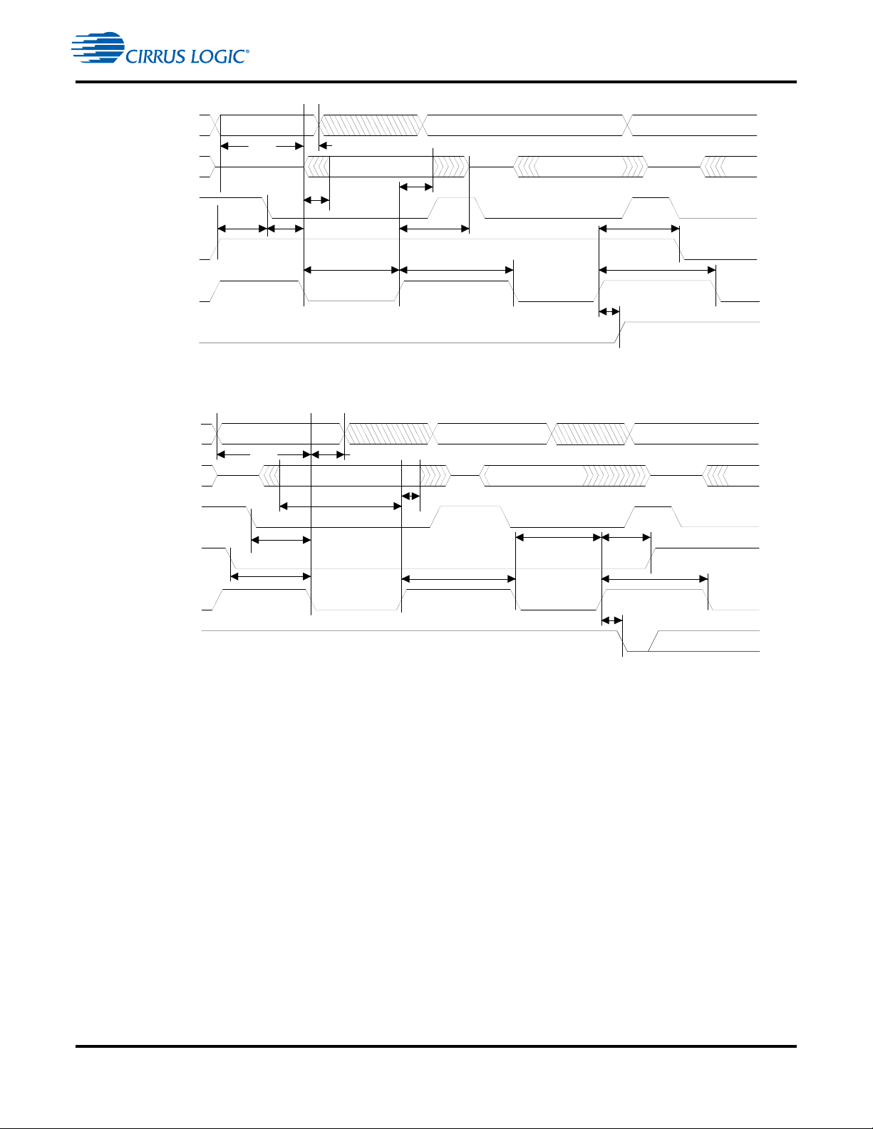
CS4970x4 Data Sheet
SCP_BSY#
SCP_CS#
SCP_CLK
SCP_MOSI
SCP_MISO
SCP_IRQ#
0
12670
56
7
t
spicss
t
spickl
t
spickh
t
spidsu
t
spidh
t
spidov
A6 A5 A0 R/W MSB LSB
MSB LSB
t
spicsh
t
spibsyl
t
spiirql
t
spiirqh
f
spisck
t
spicsdz
32-bit High Definition Audio Decoder DSP Family
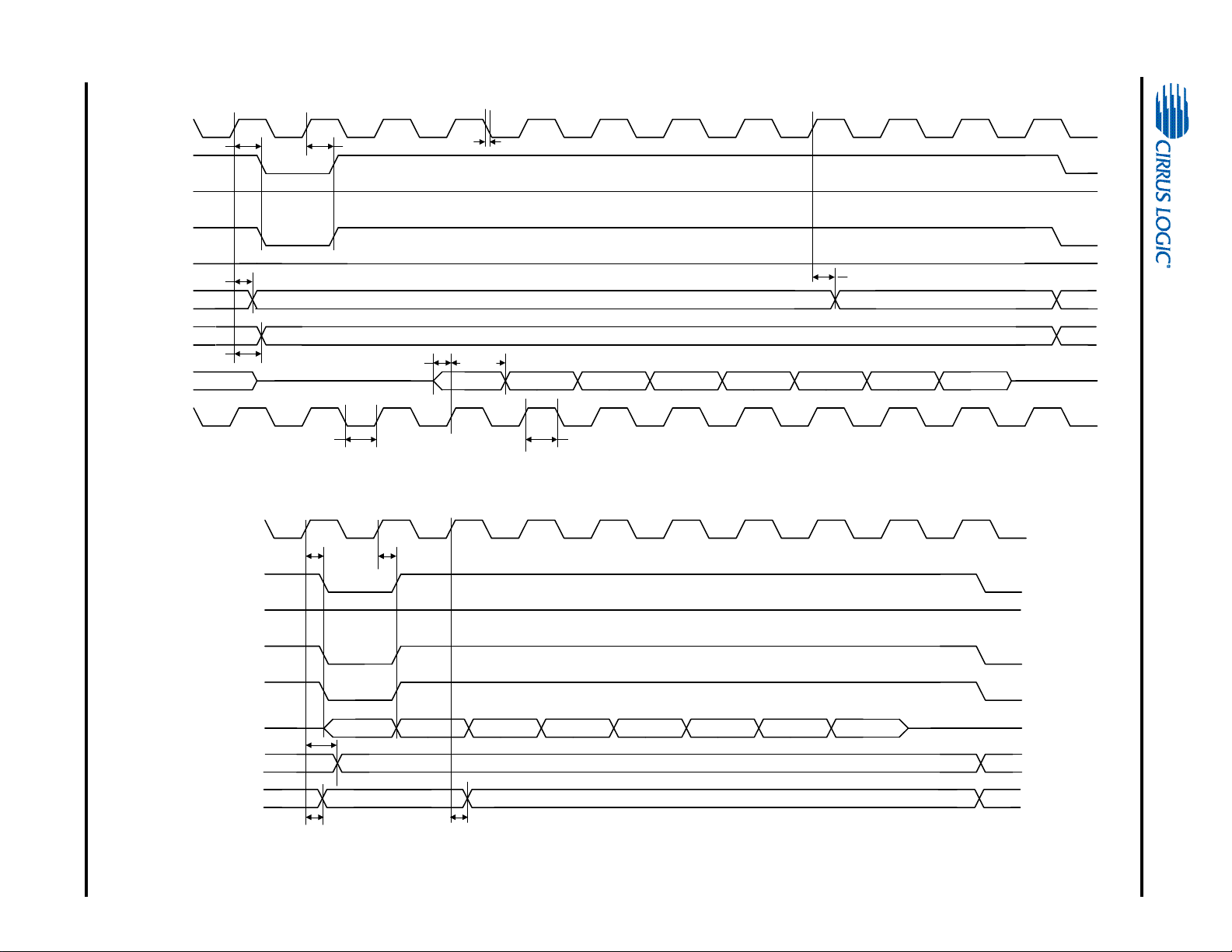
5.9 Switching Characteristics — Serial Control Port - SPI Slave Mode
Parameter Symbol Min Typical Max Units
SCP_CLK frequency1,
SCP_CS falling to SCP_CLK rising
SCP_CLK low time
SCP_CLK high time
Setup time SCP_MOSI input
Hold time SCP_MOSI input
SCP_CLK low to SCP_MISO output valid
SCP_CLK falling to SCP_IRQ rising
SCP_CS rising to SCP_IRQ falling2
SCP_CLK low to SCP_CS rising
SCP_CS rising to SCP_MISO output high-Z
SCP_CLK rising to SCP_BSY falling
1. The specification f
maximum speed of the communication port may be limited by the firmware application. Flow control using the SCP_
should be implemented to prevent overflow of the input data buffer. At boot the maximum speed is Fxtal/3.
2. When SCP1 is in SPI slave mode, very slow rise and fall times of the SCP_CLK edges may make the edges of the SCP_CLK
more susceptible to noise, resulting in non-smooth edges. Any glitch at the threshold levels of the SCP port input signals could
result in abnormal operation of the port. In systems that have noise coupling onto SCP_CLK, slow rise and fall times may cause
host communication problems. Increasing rise time makes host communication more reliable.
2
2
2
2
2
2
2
2
indicates the maximum speed of the hardware. The system designer should be aware that the actual
spisck
f
spisck
t
spicss
t
spickl
t
spickh
t
spidsu
t
spidh
t
spidov
t
spiirqh
t
spiirql
t
spicsh
t
spicsdz
t
spicbsyl
—— 25MHz
24 — — ns
20 — — ns
20 — — ns
5— —ns
5— —ns
—— 11ns
— — 20 ns
0— —ns
24 — — ns
—20 —ns
—3
DCLKP+20 — ns
*
BSY pin
Figure 3. Serial Control Port - SPI Slave Mode Timing
DS752F1 13
Page 14
32-bit High Definition Audio Decoder DSP Family
EE_CS#
SCP_CLK
SCP_MISO
SCP_MOSI
0
12670
56
7
t
spicss
t
spickl
t
spickh
t
spidsu
t
spidh
t
spidov
A6 A5 A0 R/W MSB LSB
MSB
LSB
t
spicsh
t
spicsx
f
spisck
t
spidz
t
spicsl
5.10 Switching Characteristics — Serial Control Port - SPI Master Mode
Parameter Symbol Min Typical Max Units
SCP_CLK frequency
SCP_CS falling to SCP_CLK rising
1, 2
f
spisck
3
t
spicss
—— F
— 11*DCLKP +
(SCP_CLK PERIOD)/2
CS4970x4 Data Sheet
/2 MHz
xtal
—ns
SCP_CLK low time
SCP_CLK high time
Setup time SCP_MISO input
Hold time SCP_MISO input
SCP_CLK low to SCP_MOSI output valid
SCP_CLK low to SCP_CS falling
SCP_CLK low to SCP_CS rising
t
spickl
t
spickh
t
spidsu
t
spidh
t
spidov
t
spicsl
t
spicsh
16.9 — — ns
16.9 — — ns
11 — — ns
5— —ns
—— 11ns
7— —ns
— 11*DCLKP +
—ns
(SCP_CLK PERIOD)/2
Bus free time between active SCP_CS
SCP_CLK falling to SCP_MOSI output high-Z
1. The specification f
maximum speed of the communication port may be limited by the firmware application.
2. See Section 5.7.
3. SCP_CLK PERIOD refers to the period of SCP_CLK as being used in a given application. It does not refer to a tested parameter.
indicates the maximum speed of the hardware. The system designer should be aware that the actual
spisck
t
spicsx
t
spidz
— 3*DCLKP — ns
— — 20 ns
.
Figure 4. Serial Control Port - SPI Master Mode Timing
DS752F1 14
Page 15
32-bit High Definition Audio Decoder DSP Family
SCP_BSY#
SCP_CLK
SCP_SDA
SCP_IRQ#
01 67801 7
t
iicckl
t
iicckh
t
iicsutiich
A6 A0 R/W ACK
LSB
t
iicirqh
t
iicirql
8
ACK
MSB
t
iicstp
6
t
iiccbsyl
t
iicdov
t
iicbft
t
iicstscl
t
iicckcmd
f
iicck
t
iicckcmd
t
iicf
t
iicr
5.11 Switching Characteristics — Serial Control Port - I2C Slave Mode
Parameter Symbol Min Typical Max Units
SCP_CLK frequency
SCP_CLK low time
SCP_CLK high time
SCP_SCK rising to SCP_SDA rising or falling for STAR T or
STOP condition
START condition to SCP_CLK falling
SCP_CLK falling to STOP condition
Bus free time between STOP and START conditions
Setup time SCP_SDA input valid to SCP_CLK rising
Hold time SCP_SDA input after SCP_CLK falling
SCP_CLK low to SCP_SDA out valid
SCP_CLK falling to SCP_IRQ rising
NAK condition to SCP_IRQ low
SCP_CLK rising to SCB_BSY low
1. The specification f
maximum speed of the communication port may be limited by the firmware application. Flow control using the SCP_
should be implemented to prevent overflow of the input data buffer.
2. This parameter is measured from the ViL level at the falling edge of the clock.
1
2
indicates the maximum speed of the hardware. The system designer should be aware that the actual
iicck
f
iicck
t
iicckl
t
iicckh
t
iicckcmd
t
iicstscl
t
iicstp
t
iicbft
t
iicsu
t
iich
t
iicdov
t
iicirqh
t
iicirql
t
iicbsyl
—— 400kHz
1.25 — — µs
1.25 — — µs
1.25 — — µs
1.25 — — µs
2.5 — — µs
3— —µs
100 — — ns
0— —ns
—— 18ns
——3
—3*DCLKP + 20 — ns
—3*DCLKP + 20 — ns
CS4970x4 Data Sheet
DCLKP + 40 ns
*
BSY pin
Figure 5. Serial Control Port - I2C Slave Mode Timing
DS752F1 15
Page 16

32-bit High Definition Audio Decoder DSP Family
SCP_CLK
SCP_SDA
01 67801 7
t
iicckl
t
iicckh
t
iicsutiich
A6 A0 R/W ACK
LSB
8
ACK
MSB
t
iicstp
6
t
iicdov
t
iicb
t
iicstscl
t
iicckcmd
f
iicck
t
iicckcmd
t
iicf
t
iicr
5.12 Switching Characteristics — Serial Control Port - I2C Master Mode
Parameter Symbol Min Max Units
SCP_CLK frequency
SCP_CLK low time
SCP_CLK high time
SCP_SCK rising to SCP_SDA rising or falling for START or STOP
condition
START condition to SCP_CLK falling
SCP_CLK falling to STOP condition
Bus free time between STOP and START conditions
Setup time SCP_SDA input valid to SCP_CLK rising
Hold time SCP_SDA input after SCP_CLK falling
SCP_CLK low to SCP_SDA out valid
1. The specification f
maximum speed of the communication port may be limited by the firmware application.
2. This parameter is measured from the ViL level at the falling edge of the clock.
1
2
indicates the maximum speed of the hardware. The system designer should be aware that the actual
iicck
f
iicck
t
iicckl
t
iicckh
t
iicckcmd
t
iicstscl
t
iicstp
t
iicbft
t
iicsu
t
iich
t
iicdov
— 400 kHz
1.25 — µs
1.25 — µs
1.25 — µs
1.25 — µs
2.5 — µs
3—µs
100 — ns
0—ns
—36ns
CS4970x4 Data Sheet
Figure 6. Serial Control Port - I2C Master Mode Timing
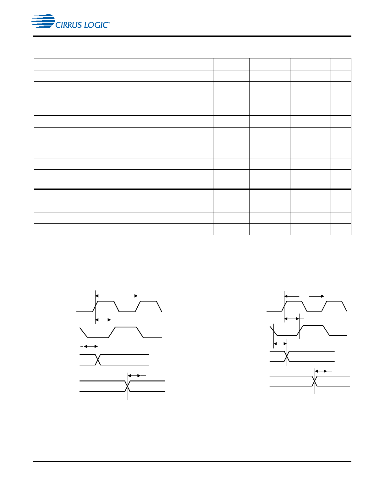
5.13 Switching Characteristics — Parallel Control Port - Intel Slave Mode
Parameter Symbol Min Typical Max Unit
Address setup before PCP_CS and PCP_RD low or PCP_CS and
PCP_WR low
Address hold time after PCP_CS and PCP_RD low or PCP_CS and
PCP_WR high
Read
DS752F1 16
t
ias
t
iah
5——ns
5——ns
Page 17

CS4970x4 Data Sheet
PCP_A[3:0]
PCP_D[7:0]
t
ias
t
icdr
t
iah
t
idd
t
irpw
t
idhr
t
idis
t
ird
t
irdtw
PCP_CS#
PCP_WR#
PCP_RD#
PCP_IRQ#
t
irdirqh
LSP MSP
32-bit High Definition Audio Decoder DSP Family
Parameter Symbol Min Typical Max Unit
Delay between PCP_RD
then PCP_CS low or PCP_CS then
PCP_RD low
Data valid after PCP_CS and PCP_RD low
PCP_CS and PCP_RD low for read
Data hold time after PCP_CS or PCP_RD high
Data high-Z after PCP_CS or PCP_RD high
PCP_CS or PCP_RD high to PCP_CS and PCP_RD low for next
1
read
PCP_CS or PCP_RD high to PCP_CS and PCP_WR low for next
1
write
PCP_RD rising to PCP_IRQ rising
Write
Delay between PCP_WR then PCP_CS low or PCP_CS then
PCP_WR
Data setup before PCP_CS or PCP_WR high
PCP_CS and PCP_WR low for write
Data hold after PCP_CS or PCP_WR high
PCP_CS or PCP_WR high to PCP_CS and PCP_RD low for next
read
low
1
t
icdr
t
idd
t
irpw
t
idhr
t
idis
t
ird
t
irdtw
t
irdirqhl
t
icdw
t
idsu
t
iwpw
t
idhw
t
iwtrd
0——ns
——18ns
24 — — ns
8——ns
——18ns
30 — — ns
30 — — ns
——12ns
0——ns
8——ns
24 — — ns
8——ns
30 — — ns
PCP_CS or PCP_WR high to PCP_CS and PCP_WR low for next
1
write
PCP_WR rising to PCP_BSY falling
1. The system designer should be aware that the actual maximum speed of the communication port may be limited by the firmware
application. Hardware handshaking on the PCP_
CS4953x4/CS4970x4 System Designer’s Guide should be consulted for the firmware speed limitations.
BSY pin/bit should be observed to prevent overflowing the input data buffer.
t
iwd
t
iwrbsyl
30 — — ns
— 2*DCLKP + 20 — ns
Figure 7. Parallel Control Port - Intel Slave Mode Read Cycle
DS752F1 17
Page 18

32-bit High Definition Audio Decoder DSP Family
t
ias
t
icdw
t
iah
t
iwpw
t
idhw
t
iwd
t
iwtrd
t
idsu
t
iwrbsyl
PCP_D[7:0]
PCP_CS#
PCP_WR#
PCP_RD#
PCP_A[3:0]
PCP_BSY#
LSP MSP
Figure 8. Parallel Control Port - Intel Slave Mode Write Cycle
CS4970x4 Data Sheet
DS752F1 18
Page 19

CS4970x4 Data Sheet
32-bit High Definition Audio Decoder DSP Family
5.14 Switching Characteristics — Parallel Control Port - Motorola Slave Mode
Symbo
Parameter
lMin Typical MaxUnit
Address setup before PCP_CS and PCP_DS low
Address hold time after PCP_CS and PCP_DS low
Read
Delay between PCP_DS then PCP_CS low or PCP_CS then
PCP_DS
Data valid after PCP_CS and PCP_DS low with PCP_R/W high
PCP_CS and PCP_DS low for read
Data hold time after PCP_CS or PCP_DS high after read
Data high-Z after PCP_CS or PCP_DS high after read
PCP_CS or PCP_DS high to PCP_CS and PCP_DS low for next
read
PCP_CS or PCP_DS high to PCP_CS and PCP_DS low for next
write
PCP_RW rising to PCP_IRQ falling
low
1
1
Write
Delay between PCP_DS then PCP_CS low or PCP_CS then
PCP_DS
Data setup before PCP_CS or PCP_DS high
PCP_CS and PCP_DS low for write
PCP_R/W setup before PCP_CS AND PCP_DS low
PCP_R/W hold time after PCP_CS or PCP_DS high
Data hold after PCP_CS or PCP_DS high
PCP_CS or PCP_DS high to PCP_CS and PCP_DS low with
PCP_R/W
low
high for next read
1
t
mas
t
mah
t
mcdr
t
mdd
t
mrpw
t
mdhr
t
mdis
t
mrd
t
mrdtw
t
mrwirqh
t
mcdw
t
mdsu
t
mwpw
t
mrwsu
t
mrwhld
t
mdhw
t
mwtrd
5——ns
5——ns
0——ns
— — 19 ns
24 — — ns
8——ns
— — 18 ns
30 — — ns
30 — — ns
— — 12 ns
0——ns
8——ns
24 — — ns
24 — — ns
8——ns
8——ns
30 — — ns
PCP_CS or PCP_DS high to PCP_CS and PCP_DS low for next
1
write
PCP_RW rising to PCP_BSY falling
1. The system designer should be aware that the actual maximum speed of the communication port may be limited by the firmware
application. Hardware handshaking on the PCP_
CS4953x4/CS4970x4 System Designer’s Guide should be consulted for the firmware speed limitations.
DS752F1 19
BSY pin/bit should be observed to prevent overflowing the input data buffer.
t
mwd
t
mrwbsyl
30 — — ns
—2*DCLKP + 20—ns
Page 20
32-bit High Definition Audio Decoder DSP Family
t
mas
t
mcdr
t
mah
t
mdd
t
mrpw
t
mdhr
t
mdis
t
mrd
t
mrdtw
t
mrwsu
t
mrwhld
PCP_A[3:0]
PCP_AD[7:0]
PCP_CS#
PCP_WR#
PCP_DS#
PCP_IRQ#
t
mrwirqh
LSP MSP
t
mas
t
mdsu
t
mdhw
t
mwd
t
mwtrd
t
mwpw
t
mcdw
t
mrwsu
t
mrwhld
mah
t
PCP_A[3:0]
PCP_AD[7:0]
PCP_CS#
PCP_WR#
PCP_DS#
PCP_IRQ#
t
mrwirql
LSP MSP
Figure 9. Parallel Control Port - Motorola Slave Mode Read Cycle Timing
CS4970x4 Data Sheet
Figure 10. Parallel Control Port - Motorola Slave Mode Write Cycle Timing
DS752F1 20
Page 21
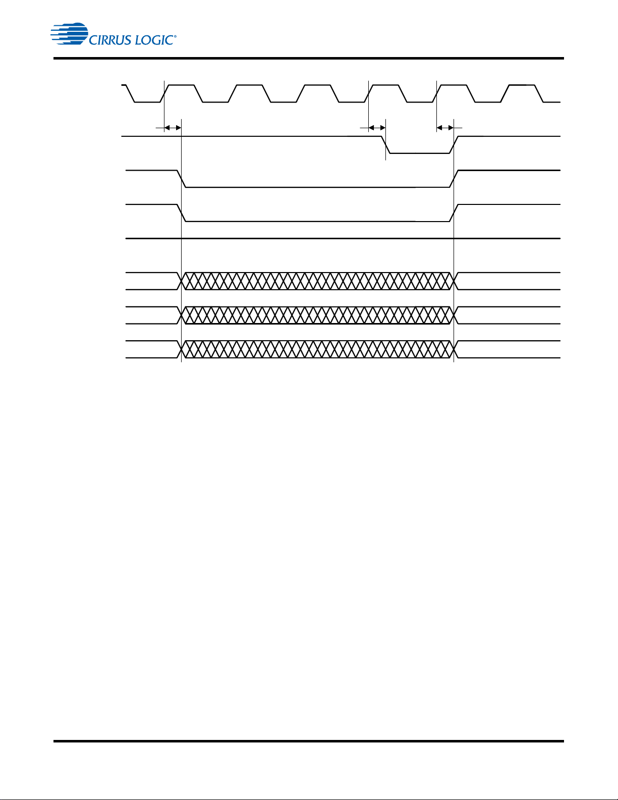
32-bit High Definition Audio Decoder DSP Family
DAI_SCLK
DAI_DATAn
t
daidh
t
daidsu
DAI_SCLK
DAI_LRCLK
DAIn_DATAn
t
daislrts
Tdaiclkp
DAI_SCLK
DAI_LRCLK
t
daisstlr
Tdaiclkp
DAIn_DATAn
5.15 Switching Characteristics — Digital Audio Slave Input Port
Parameter Symbol Min Max Unit
CS4970x4 Data Sheet
DAI_SCLK period
DAI_SCLK duty cycle
DAI_LRCLK transition from DAI_SCLK active edge
DAI_SCLK active edge from DAI_LRCLK transition
Setup time DAI_DATAn
Hold time DAI_DATAn
Note: In these diagrams, falling edge is the inactive edge of DAI_SCLK.
Figure 11. Digital Audio Input (DAI) Port Timing Diagram
T
daiclkp
40 — ns
—4555%
t
daisstlr
t
daislrts
t
daidsu
t
daidh
10 — ns
10 — ns
10 — ns
5—ns
DS752F1 21
Figure 12. DAI Slave Timing Diagram
Page 22
32-bit High Definition Audio Decoder DSP Family
DAO_MCLK
DAO_SCLK
DAO_LRCLK
DAOn_DATAn
t
daomlclk
t
daomsck
t
daomdv
t
daomlrts
DAO_MCLK
DAO_SCLK
DAO_LRCLK
DAOn_DATAn
t
daomlclk
t
daomsck
t
daomdv
t
daomlrts
Note: In these diagrams, falling edge is the inactive edge of DAO_SCLK.
5.16 Switching Characteristics — Digital Audio Output Port
Parameter Symbol Min Max Unit
CS4970x4 Data Sheet
DAO_MCLK period
DAO_MCLK duty cycle
DAO_SCLK period for Master or Slave mode
1
DAO_SCLK duty cycle for Master or Slave mode
Master Mode (Output A1 Mode)
DAO_SCLK delay from DAO_MCLK rising edge,
1
1,2
T
daomclk
—
T
daosclk
40 — ns
45 55 %
40 — ns
— 40 60 %
t
daomsck
— 19 ns
DAO_MCLK as an input
DAO_SCLK delay from DAO_LRCLK transition
DAO_LRCLK delay from DAO_SCLK transition
DAO1_DATA[3..0], DAO2_DATA[1..0]
delay from DAO_SCLK transition
3
Slave Mode (Output A0 Mode)
DAO_SCLK active edge to DAO_LRCLK transition t
DAO_LRCLK transition to DAO_SCLK active edge t
DAO_Dx delay from DAO_SCLK inactive edge t
1. Master mode timing specifications are characterized, not production tested.
2. Master mode is defined as the CS4970x4 driving both DAO_SCLK, DAO_LRCLK. When MCLK is an input, it is divided to produce
DAO_SCLK, DAO_LRCLK.
3. This timing parameter is defined from the non-active edge of DAO_SCLK. The active edge of DAO_SCLK is the point at which the
data is valid.
4. Slave mode is defined as DAO_SCLK, DAO_LRCLK driven by an external source.
3
3
4
t
daomlrts
t
daomstlr
t
daomdv
daosstlr
daoslrts
daosdv
— 8ns
— 8ns
— 10 ns
10 — ns
10 — ns
— 12.5 ns
DS752F1 22
Figure 13. Digital Audio Port Output Timing Master Mode
Page 23
Figure 14. Digital Audio Output Timing, Slave Mode (Relationship LRCLK to SCLK)
DAO_SCLK
DAO_LRCLK
DAO_Dx
t
daoslrts
t
daosclk
DAO_SCLK
DAO_LRCLK
t
daosstlr
t
daosdv
t
daosclk
DAO_Dx
Note: In these diagrams, Falling edge is the inactive edge of DAO_SCLK
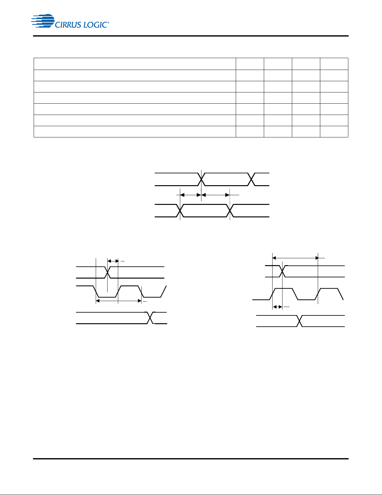
5.17 Switching Characteristics — SDRAM Interface
Refer to Figure 15 through Figure 18.
(SD_CLKOUT = SD_CLKIN)
CS4970x4 Data Sheet
32-bit High Definition Audio Decoder DSP Family
Parameter Symbol Min Typical Max Unit
SD_CLKIN high time
SD_CLKIN low time
SD_CLKOUT rise/fall time
SD_CLKOUT Frequency
SD_CLKOUT duty cycle
SD_CLKOUT rising edge to signal valid
Signal hold from SD_CLKOUT rising edge
SD_CLKOUT rising edge to SD_DQMn valid
SD_DQMn hold from SD_CLKOUT rising edge
SD_DATA valid setup to SD_CLKIN rising edge
SD_DATA valid hold to SD_CLKIN rising edge
SD_CLKOUT rising edge to ADDRn valid
t
sdclkh
t
sdclkl
t
sdclkrf
——
—
t
sdcmdv
t
sdcmdh
t
sddqv
t
sddqh
t
sddsu
t
sddh
t
sdav
2.3 ——ns
2.3 ——ns
——1ns
45 — 55 %
——3.8 ns
— 1.1 — ns
— 3.8 — ns
1.38 ——ns
1.3 ——ns
2.1 ——ns
— 3.8 — ns
150 — MHz
DS752F1 23
Page 24
DS752F1 24
SD_CLKOUT
SD_CS#
SD_RAS#
SD_CAS#
SD_WE#
SD_DQMn
SD_An
SD_Dn
t
sddsu
t
sdclkrf
t
sdcmdv
t
sdav
t
sddqv
t
sdcmdh
t
sddh
t
sddqh
CAS=2
LSP0 MSP0
LSP3 MSP3
SD_CLKIN
t
sdclkl
t
sdclkh
00
11
LSP1 MSP1 LSP2 MSP2
SD_CLKOUT
SD_CS#
SD_RAS#
SD_CAS#
SD_WE#
t
sdcmdv
t
sdcmdh
SD_Dn
LSP0 MSP0 LSP1 MSP1 LSP2 MSP2 LSP3 MSP3
SD_An
SD_DQMn
t
sddqh
00 11
t
sddqv
t
sdav
Figure 15. External Memory Interface - SDRAM Burst Read Cycle
Figure 16. External Memory Interface - SDRAM Burst Write Cycle
32-bit High Definition Audio Decoder DSP Family
CS4970x4 Data Sheet
Page 25
CS4970x4 Data Sheet
SD_CLKOUT
SD_CS#
SD_RAS#
SD_CAS#
SD_WE#
SD_DQMn
SD_An
SD_Dn
t
sdcmdv
t
sdcmdh
t
sdcmdv
32-bit High Definition Audio Decoder DSP Family
Figure 17. External Memory Interface - SDRAM Auto Refresh Cycle
DS752F1 25
Page 26

CS4970x4 Data Sheet
SD_CLKOUT
SD_CS#
SD_RAS#
SD_CAS#
SD_WE#
SD_DQMn
SD_An
SD_Dn
OPCODE
t
sdcmdv
t
sdcmdh
32-bit High Definition Audio Decoder DSP Family
Figure 18. External Memory Interface - SDRAM Load Mode Register Cycle
DS752F1 26
Page 27

6 Ordering Information
The CS4970x4 family part number is described as follows:
CS497NNI-XYZ
where
NN - Product Number Variant
I - ROM ID Number
X - Product Grade
Y - Package Type
Z - Lead (Pb) Free
Table 4. Ordering Information
Part No. Status Grade Temp. Range Package
CS497014-CVZ Active Commercial 0 to +70 °C 128-pin LQFP
CS47014-CVZR
CS497024-CVZ Active Commercial 0 to +70 °C 128-pin LQFP
CS497024-CVZR
1
1
Active Commercial 0 to +70 °C
Active Commercial 0 to +70 °C
CS4970x4 Data Sheet
32-bit High Definition Audio Decoder DSP Family
1. R = Tape and reel
Note: Please contact the factory for availability of the -D (automotive grade) package.
7 Environmental, Manufacturing, and Handling Information
Table 5. Environmental, Manufacturing, & Handling Information
Model Number Peak Reflow Temp MSL Rating* Max Floor Life
CS497014-CVZ 260 °C 3 7 Days
CS47014-CVZR 260 °C 3 7 Days
CS497024-CVZ 260 °C 3 7 Days
CS497024-CVZR 260 °C 3 7 Days
* MSL (Moisture Sensitivity Level) as specified by IPC/JEDEC J-STD-020.
DS752F1 27
Page 28
8 Device Pin-Out Diagram
GPIO2
GPIO1
GPIO0, EE_CS#
XTO
VDD7
GND7
VDDIO7
XTI
GNDIO7
GNDA
PLL_REF_RES
VDDA (3.3V)
VDD8
GND8
GPIO13, DAI1_DATA2, TM2, DSD2
GPIO14, DAI1_DATA3, TM3, DSD3
DAI1_DATA0, TM0, DSD0
GPIO12, DAI1_DATA1, TM1, DSD1
GPIO6, PCP_CS#, SCP2_CS#
GPIO38, PCP_WR# / DS#, SCP2_CLK
VDD6
GND6
GPIO10, PCP_A2 / A10, SCP2_MOSI
GPIO8, PCP_IRQ#, SCP2_IRQ#
GPIO37, SCP1_BSY#, PCP_BSY#
VDDIO6
GPIO11, PCP_A3, AS#, SCP2_MISO / SDA
GNDIO6
GPOI9, SCP1_IRQ#
GPIO34, SCP1__MISO / SDA
GPIO33, SCP1_MOSI
GPIO35, SCP1_CLK
VDD5
VDDIO5
GND5
GNDIO5
SD_CAS#
SD_RAS#
SD_A3, EXT_A3
SD_A2, EXT_A2
SD_A1, EXT_A1
SD_A0, EXT_A0
SD_A10, EXT_A10
SD_A11, EXT_A11
VDD4
GND4
SD_CS#
SD_A4, EXT_A4
SD_A5, EXT_A5
SD_A6, EXT_A6
SD_A7, EXT_A7
SD_A8, EXT_A8
SD_CLKEN
SD_A9, EXT_A9
VDDIO4
GNDIO4
SD_CLKOUT
SD_CLKIN
SD_D10, EXT_D10
SD_D11, EXT_D11
SD_D12, EXT_D12
VDD3
GND3
SD_D13, EXT_D13
SD_D14, EXT_D14
SD_D15, EXT_D15
SD_DQM1
SD_D7, EXT_D7
SD_D6, EXT_D6
VDDIO3
GNDIO3
SD_D5, EXT_D5
SD_DQM0
SD_D4, EXT_D4
SD_D3, EXT_D3
SD_D2, EXT_D2
GPIO17, DAO1_DATA3 / XMTA
GPIO15, DAO1_DATA1, HS1
DAO1_DATA0, HS0
DAO1_LRCLK
DAI1_LRCLK, DSD4
DAO_MCLK
GPIO20, DAO2_DATA2
DAI1_SCLK, DSD_CLK
VDD1
GND1
DAO1_SCLK
GPIO16, DAO1_DATA2, HS2
GPIO23,
DAO2_LRCLK
RESET#
VDDIO1
GPIO22, DAO2_SCLK
GNDIO1
GPIO18, DAO2_DATA0, HS3
GPIO19, DAO2_DATA1, HS4
VDD2
GND2
GPIO26, DAO2_DATA3 / XMTB
VDDIO2
GNDIO2
SD_WE#
SD_D0, EXT_D0
SD_D1, EXT_D1
SD_D8, EXT_D8
SD_D9, EXT_D9
SD_A12, EXT_A12
SD_BA1, EXT_A14
SD_BA0, EXT_A13
GPIO7, SCP1_CS#, IOWAIT
VDDIO8
GNDIO8
EXT_A15
EXT_A16
EXT_A17
EXT_A18
EXT_A19
EXT_CS1#
EXT_OE#
EXT_WE#
GPIO3, DDAC
TEST
DBDA
DBCK
XTAL_OUT
GPIO43, BDI_CLK, DAI2_SCLK
GPIO42, BDI_REQ# , DAI2_LRCLK, PCP_IRQ# / BSY#
BDI_DATA, DAI2_DATA, DSD5
EXT_CS2#
10
15
20
25
30
5
35
1
125
120
115
110
105
95
90
85
80
75
70
65
100
40
45
50
55
60
CS497xx4
128-Pin LQFP
8.1 128-Pin LQFP Pin-Out Diagram
CS4970x4 Data Sheet
32-bit High Definition Audio Decoder DSP Family
DS752F1 28
Figure 19. 128-Pin LQFP Pin-Out Diagram
Page 29

9 Package Mechanical Drawings
D1
D
E1
E
1
e
L
b
A1
A
9.1 128-Pin LQFP Package Drawing
CS4970x4 Data Sheet
32-bit High Definition Audio Decoder DSP Family
Figure 20. 128-Pin LQFP Package Drawing
Table 6. 128-Pin LQFP Package Characteristics
DIM
A — — 1.60 — — .063”
A1 0.05 — 0.15 .002” — .006”
b 0.17 0.22 0.27 .007” .009” .011”
D 22.00 BSC .866”
D1 20.00 BSC .787”
E 16.00 BSC .630”
E1 14.00 BSC .551”
e 0.50 BSC .020”
q 0° 3.5 7° 0° 3.5 7°
L 0.45 0.60 0.75 .018” .024” .030”
L1 1.00 REF .039” REF
ddd 0.08 .003”
MIN NOM MAX MIN NOM MAX
MILLIMETERS INCHES
TOLERANCES OF FORM AND POSITION
DS752F1 29
Page 30

32-bit High Definition Audio Decoder DSP Family
10 Revision History
Revision Date Changes
PP9 Novembe r, 2010 Added “Status” column and footnote 1 to Table 4.
Added Tj conditions to Section 5.2.
Changed 500 ma to 350 ma in Section 5.4.
PP10 March, 2011
PP11 February, 2012
PP12 October, 2013 Updated note in Section 2 overview. Minor change to Section 2.1 title.
F1 February, 2014
Updated Section 5.15 “Switching Charac teristics — Digi tal Aud io Slave Input Po rt”
on page 21.
Updated Section 5.16 “Switching Characteristics — Digital Audio Output Port” on
page 22.
Added max internal DCLK frequency and min internal DCLK period to Section 5.8.
Added notes to Section 5.9. Updated tspickl and tspickh values in Section 5.10.
Updated tdaosdv max value in Section 5.16.
Updated note in Section 2 overview regarding CS4970x4. Changed status of
CS497024-CVZ and CS497024-CVZR to “Active” in Table 4.
CS4970x4 Data Sheet
DS752F1 30
Page 31

CS4970x4 Data Sheet
Contacting Cirrus Logic Support
For all product questions and inquiries, contact a Cirrus Logic Sales Representative.
To find the one nearest you, go to www.cirrus.com.
IMPORTANT NOTICE
Cirrus Logic, Inc. and its subsidiaries (“Cirrus”) belie ve that the inform ation contai ned in this docu ment is accurate and reliable. However, the in formatio n is subject to
change without notice an d is provided “AS IS” withou t warranty of any kind ( express or implied). Cus tomers are advised to obta in the latest version of relevant
information to verify, befo re pla ci ng or ders , that inf o rmat io n bein g re li ed on is c urr ent and c ompl et e. Al l pr od uct s are sol d s ubject to the terms and conditions of sale
supplied at the time of order acknowle dgme nt, includin g those pertainin g to war ranty, in demni fication, a nd lim itation of lia bility. No responsibility is assumed by C irrus
for the use of this information, including use of this information as the basis for manufacture or sale of any items, or for infringement of patents or other rights of third
parties. This document i s t he prop er t y of Ci rr us a nd by fu rn i shi ng thi s i nfo r mat i on, Ci r ru s gr an ts no li c e nse , ex pr es s or impl ied under any patents, mask work rights,
copyrights, trademarks, trade secrets or other intellectual property rights. Cirrus owns the copy rights associated with th e information contained herein and gives
consent for copies to be made of the information only for use within your organization with respect to Cirrus integrated circuits or other products of Cirrus. This consent
does not extend to other copying such as copying for general distribution, advertising or promotional purposes, or for creating any work for resale.
CERTAIN APPLICATIONS USING SEMICONDUCTOR PRODUCTS MAY INVOLVE POTENTIAL RISKS OF DEATH, PERSONAL INJURY, OR SEVERE
PROPERTY OR ENVIRONMEN TAL DAMAGE (“CRITIC AL APPLICATIONS”). CIRRUS PR ODUCTS ARE NOT DESIGNED, AUTHO RIZED OR WAR RANTED FOR
USE IN PRODUCTS SURGICALLY IMPLANTED INTO THE BODY, AUTOMOTIVE SAFETY OR SECURITY DEVICES, LIFE SUPPORT PRODUCTS OR OTHER
CRITICAL APPLICATIONS. INCLUSION OF CIRRUS PRODUCTS IN SUCH APPLICATIONS IS UNDERSTOOD TO BE FULLY AT THE CUSTOMER’S RISK AND
CIRRUS DISCLAIMS AND MAKES NO WARRANTY, EX PRESS, STATUTORY OR IMPLIED, INCLUDING THE IMPLIED WARRANTIES OF MERCHANTABILITY
AND FITNESS FOR PARTICULAR PURPOSE , WITH REGARD TO ANY CIRRUS PRODUCT THAT IS USED IN SUCH A MANNER. IF THE CUSTOMER OR
CUSTOMER’S CUSTOMER USES OR PERMITS THE USE OF CIRRUS PRODUCTS IN CRITICAL APPLICATIONS, CUSTOMER AGREES, BY SUCH USE, TO
FULLY INDEMNIFY CIRRUS, ITS OFFICERS, DIRECTORS, EMPLOYEES, DISTRIBUTORS AND OTHER AGENTS FROM ANY AND ALL LIABILITY, INCLUDING
ATTORNEYS’ FEES AND COSTS, THAT MAY RESULT FROM OR ARISE IN CONNECTION WITH THESE USES.
Cirrus Logic, Cirrus, Cirrus Logic logo designs, Cirrus Framework, and DSP Condenser are trademarks of Cirrus Logic, Inc. All other brand and product names in this
document may be trademarks or service marks of their respective owners.
THX is a registered trademark of THX, Ltd. THX Select 2 and THX Ultra 2 are trademarks of THX, Ltd.
Dolby, Dolby Digital , Dolby Headphone, Virt ual Sp eaker, Pro Log ic, Aud istry , and Dol by Vol ume are re giste red tr ademarks of Dolb y Labo rator ies, I nc. AA C, AC-3 ,
Dolby TrueHD, and Dolby Volume 258 are trademarks of Dolby Laboratories, Inc. Supply of an implementation of Dolby Technology does not convey a license nor
imply a right under any patent, or an y other industria l or Intellectual Property Right of Dolby Labo ratories, to use the Imple mentation in a ny finished end-user or readyto-use final product. It is hereby notified that a license for such use is required from Dolby Laboratories.
DTS and DTS Neo:6 are registered trademarks of the Digital Theater Systems, Inc. DTS-ES 96/24, DTS-ES, DTS 6.1, DTS 96/24, DTS Neural Surround, and DTS
Express are trademarks of Digital Theat er Systems, I nc. It is h ereby notified that a thir d-party lic ense from DTS is nec essary to distribute software of DTS in any
finished end-user or ready-to-use final product.
SRS, SRS 3D, SRS CS Auto, SRS CS Headphone, SRS Circl e Cinema 3D, SRS Circle Surround, SRS Circle Surround II, SRS GEQ, SRS Hardlimiter, SRS
Headphone, SRS Headphone 36 0, SRS HP F, SR S Stud ioSound HD, SRS TruEQ, SRS TruMedia, SR S TruS urround, SRS TruSurround XT, SRS TruSurroun d HD,
SRS TruSurround HD4, SRS TruVol ume, S RS VIP+, SRS WOW, SRS WOW XT, SRS WOW HD are either trademar ks or r egi st er ed t r ademar k s of SRS Labs, Inc.
SRS, SRS 3D, SRS CS Auto, SRS CS Headphone, SRS Circl e Cinema 3D, SRS Circle Surround, SRS Circle Surround II, SRS GEQ, SRS Hardlimiter, SRS
Headphone, SRS Headphone 36 0, SRS HP F, SR S Stud ioSound HD, SRS TruEQ, SRS TruMedia, SR S TruS urround, SRS TruSurround XT, SRS TruSurroun d HD,
SRS TruSurround HD4, SRS TruVolume, SRS VIP+, SRS WOW, SRS WOW XT, SRS WOW HD technologies are incorporated under license from SRS Labs, Inc.
SRS, SRS 3D, SRS CS Auto, SRS CS Headphone, SRS Circl e Cinema 3D, SRS Circle Surround, SRS Circle Surround II, SRS GEQ, SRS Hardlimiter, SRS
Headphone, SRS Headphone 36 0, SRS HP F, SR S Stud ioSound HD, SRS TruEQ, SRS TruMedia, SR S TruS urround, SRS TruSurround XT, SRS TruSurroun d HD,
SRS TruSurround HD4, SRS TruVol u me, SRS V I P+, SRS WOW, SRS WOW XT , SRS WOW HD t ec hnol og i es i nco rp or at ed in t he Cir r us Log ic CS4 953xx products
are owned by SRS Labs, a U.S. Co rpor ation and licensed to Cirrus Logi c , I nc . P ur cha ser of Cirrus Logic CS4953xx products mus t s ign a license for use of the ch ip
and display of the SRS Labs trademarks. Any products incorporating the Cirrus Logic CS4953xx products must be sent to SRS Labs for review. SRS, SRS 3D, SRS
CS Auto, SRS CS Headphone, SRS Circle Cinema 3D, SRS Circle Surround, SRS Circle Surround II, SRS GEQ, SRS Hardlimiter, SRS Headphone, SRS Headphone
360, SRS HPF, SRS Studio-Sound HD, SRS TruEQ, SRS TruMedia, SRS TruSurround, SRS TruSurround XT, SRS TruSurround HD, SRS TruSurround HD4, SRS
TruVolume, SRS VIP+, SRS WOW, SRS WOW XT, S RS WOW HD technologies are protected un der US and forei gn patents issue d and/or pending. Neither the
purchase of the Cirrus Logic CS4953xx products, nor the corresponding sale of audio enhancement equipment conveys the right to sell commercialized recordings
made with any SRS technology/solution. SRS Labs requires all set makers to comply with all rules and regulations as outlined in the SRS Trademark Usage Manual.
Motorola is a registered trademark of Motorola, Inc. SPI is a trademark of Motorola, Inc.
Intel is a registered trademark of Intel Corporat ion .
I2C is a trademark of Philips Semiconductor.
32-bit High Definition Audio Decoder DSP Family
DS752F1 31
 Loading...