

CS4923/4/5/6/7/8/9
Multi-Channel Digital Audio Decoders
l CS4923/4/5/6/7/8 features
— Optional Virtual 3D Output
— Simulated Surround and Programmable Effects
— Real Time Autodetection of Dolby Digital
®
DTS
, MPEG Multi-Channel and PCM
®
,
— Flexible 6-channel master or slave output
l CS4923/4/5/6/7/8/9 features
— IEC60958/61937 transmitter for co mpressed-
data or linear-PCM output
— Dedicated 8 kilobyte input buffer
— DAC clock via analog phase-locked loop
— Dedicated byte wide or serial host interface
— Multiple compressed data input modes
— PES layer decode for A/V synchronization
— 96-kHz-capable PCM I/O, master or slave
— Optional external memory and auto-boot
— +3.3-V CMOS low-power, 44-pin package
l CS4923/4/5/6 features
— Capable of Dolby Digital® Group A Performance
— Dolby bass manager and crossover filters
— Dolby Surround Pro Logic
l CS4925/7: MPEG-2 Multi-Channel Decode r
l CS4926/8: DTS Multi-Channel Decoder
l CS4929: AAC 2-Channel (Low Complexity)
®
Decoding
and MPEG-2 Stereo Decoder
Description
The CS4923/4/5/6/7/8 is a family of multi-channel digital
audio decoders, with the exception of the CS4929 as the
only stereo digital audio decoder. The CS4923/4/5/6 are
designed for Dolby Digital and MPEG-2 Stereo decoding. In
addition the CS4925 adds MPEG-2 multi-channel decoding
capability and the CS4926 provides DTS decoding. The
CS4927 is an MPEG-2 multi-channel decoder and the
CS4928 is a DTS multi-channe l decoder. The CS492 9 is an
AAC 2-channel and MPEG-2 stereo decoder. Each one of
the CS4923/4/5/6/7/8/9 provides a complete and flexible
solution for multi-channel (or stereo in the case of the
CS4929) audio decoding in home A/V receiver/amplifiers,
DVD movie players, out-board decoders, laser- disc players,
HDTV sets, head-end decoders, set-top boxes, and similar
products.
Cirrus Logic’s Crystal Audio Divisio n provides a complete set
of audio decoder and auxiliary audio DSP application
programs for various applications. For all complementary
analog and digital audio I/O, Crystal Audio also provides a
complete set of high-quality audio peripherals including:
multimedia CODECs, stereo A/D and D/A converters and
IEC60958 interfaces. Of special note, the CS4226 is a
complementary CODEC providing a digital receiver, stereo
A/D converters, and six 20-bit DACs in o ne p ackage.
ORDERING INFORMATION
CS4923xx-CL 44-pin PLCC (xx = ROM revision)
CRD4923 Reference design with CS4226
CDB4923 Evaluation board
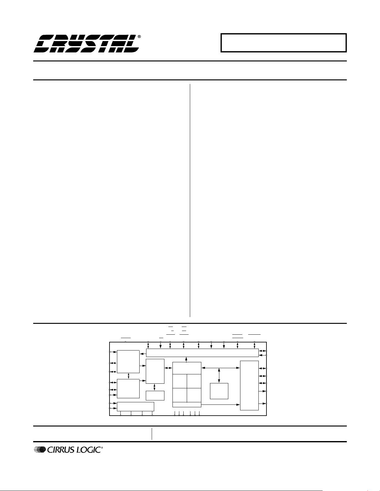
EMAD7:0,
Digital
Audio
Input
PLL
Clock Manager
VA
FILT1
CMPDAT,
SDATAN2
CMPCLK,
SCLKN2
CMPREQ,
LRCLKN2
SCLKN1,
STCCLK2
LRCLKN1
SDATAN1
CLKIN
CLKSEL
RESET
Compressed
Data Input
Interface
Interface
FILT2 AGND
Preliminary Product Information
P.O. Box 17847, Austin, Texas 78760
(512) 445 7222 FAX: (512) 445 7581
http://www.cirrus.com
RD
,
WR
,
DAT A7:0,
GPIO7:0
Framer
Shifter
Input
Buffer
Controller
RAM Input
Buffer
R/W,
EMOE
CS
GPIO11
DSP Processing
Program
Memory
Program
Memory
DGND[3:1] VD[3:1]
SCDIO,
DS
,
SCDOUT,
,
ROM
PSEL,
EMWR
,
GPIO10
Parallel or Serial Host Interface
24-Bit
RAM
RAM
Data
Memory
ROM
Data
Memory
STC
GPIO9
A0,
SCCLK
RAM
Output
Buffer
A1,
SCDIN
ABOOT
INTREQ
,
EXTMEM
GPIO8
Output
Formatter
,
DD
DC
MCLK
SCLK
LRCLK
AUDAT A[2.0]
XMT958
This document contains information for a new product.
Cirrus Logic reserves the right to modify this product without notice.
Copyright Cirrus Logic, Inc. 1999
(All Rights Reserved)
AUG ‘99
DS262F2
1

TABLE OF CONTENTS
1. CHARACTERISTICS AND SPECIFICATIONS ........................................................................ 4
ABSOLUTE MAXIMUM RATINGS ............................................................................................4
RECOMMENDED OPERATING CONDITIONS........................................................................4
DIGITAL D.C. CHARACTERISTICS..........................................................................................4
POWER SUPPLY CHARACTERISTICS...................................................................................4
SWITCHING CHARACTERISTICS—RESET............................................................................5
SWITCHING CHARACTERISTICS—CMPDAT, CMPCLK........................................................6
SWITCHING CHARACTERISTICS—CLKIN .............................................................................7
SWITCHING CHARACTERISTICS—INTEL
SWITCHING CHARACTERISTICS—MOTOROLA
SWITCHING CHARACTERISTICS—DIGITAL AUDIO INPUT................................................16
SWITCHING CHARACTERISTICS—DIGITAL AUDIO OUTPUT............................................18
2. FAMILY OVERVIEW ..............................................................................................................20
2.1 Multi-channel Decoder Family of Parts ............................................................................21
2.2 Document Strategy ..........................................................................................................21
2.2.1 Hardware Documentation ...............................................................................22
2.2.2 CS4923/4/5/6/7/8/9 Application Code User’s Guides ..................................... 22
2.3 Using the CS4923/4/5/6/7/8/9 ..........................................................................................22
3. TYPICAL CONNECTION DIAGRAMS ...................................................................................23
3.1 Multiplexed Pins ...............................................................................................................23
3.2 Termination Requirements ...............................................................................................24
3.3 Phase Locked Loop Filter ................................................................................................24
4. POWER ..................................................................................................................................31
4.1 Decoupling .......................................................................................................................31
4.2 Analog Power Conditioning ..............................................................................................31
4.3 Pads .................................................................................................................................31
5. CLOCKING ............................................................................................................................. 32
6. CONTROL .............................................................................................................................. 33
6.1 Boot and Control Mode Overview ....................................................................................33
6.2 Parallel Host Interface ......................................................................................................34
6.2.1 Intel Parallel Host Mode ..................................................................................34
6.2.2 Motorola Parallel Host Mode ...........................................................................36
6.3 SPI Serial Host Interface ..................................................................................................36
6.3.1 SPI Write .........................................................................................................37
6.3.2 SPI Read .........................................................................................................37
CS4923/4/5/6/7/8/9
®
HOST MODE.....................................................8
®
HOST MODE ........................................10
Contacting Cirrus Logic Support
For a complete listing of Direct Sales, Distributor, and Sales Representative contacts, visit the Cirrus Logic web site at:
http://www.cirrus.com/corporate/contacts/
Dolby, Dolby Digital, and Pro Logic are registered trademarks of Dolby Laboratories Licensing Corporation.
Intel is a registered trademark of Intel Corporation.
Motorola is a registered trademark of Motorola, Inc.
2
I
C is a registered trademark of Philips Semiconductor.
All other names are trademarks, registered trademarks, or service marks of their respective companies.
Preliminary product information describes products whi c h are i n production, but for wh ic h ful l characterization data i s not yet available. Advance p roduct infor-
mation describes products which are in development and subject to development changes. Cirrus Logic, Inc. has made best efforts to ensure that the information
contained in this document is accur ate and reli able. However , the i nformati on is sub ject to change with out no tice and i s provi ded “AS IS” wit hout warran ty of
any kind (express or implied) . No responsibility is assumed by Cirrus Logic, Inc. for the use of this information, nor for infringements of patents or other rights
of third parties. This document is the propert y of Cirru s Logic, Inc. and implie s no licen se under patents, copyri ghts, trademarks, or tr ade secrets. No part of
this publication may be copied, reproduced , stored in a retrieval system, or transmitted, in any form or by any means (electro nic, mechanical, photographic, or
otherwise) without the pri or wri tt en consen t of Ci rrus Logic, Inc. Items from any Cirrus Logi c websi t e or di sk may be print ed for use by the user. However, no
part of the printout or electronic files may be copied, reproduced, stored in a retrieval system, or transmitted, in any form or by any means (electronic, mechanical,
photographic, or otherwise) without the prior written consent of Cirrus Logic, Inc.Furthermore, no part of this publication may be used as a basis for manufacture
or sale of any items without the prior written consent of Cirrus Logic, Inc. The names of products of Cirrus Logic, Inc. or other vendors and suppliers appearing
in this document may be trademarks or service marks of their respective owners which may be registered in some jurisdictions. A list of Cirrus Logic, Inc. trademarks and service marks can be found at http://www.cirrus.com.
2 DS262F2

CS4923/4/5/6/7/8/9
6.4 I2C Serial Host Interface .................................................................................................. 39
6.4.1 I
6.4.2 I
6.5 External Memory .............................................................................................................. 41
6.5.1 External Memory and Autoboot ...................................................................... 43
7. DIGITAL INPUT & OUTPUT .................................................................................................. 44
7.1 Digital Audio Formats ....................................................................................................... 44
7.2 Digital Audio Input Port ....................................................................................................46
7.3 Compressed Data Input Port ........................................................................................... 46
7.4 Parallel Digital Audio Data Input ......................................................................................46
7.5 Digital Audio Output Port ................................................................................................. 47
7.5.1 IEC60958 Output ............................................................................................ 48
8. PIN DESCRIPTIONS .............................................................................................................. 49
9. PACKAGE DIMENSIONS ...................................................................................................... 54
LIST OF FIGURES
Figure 1. RESET Timing.................................................................................................................. 5
Figure 2. Serial Compressed Data Timing ....................................................................................... 6
Figure 3. CLKIN with CLKSEL = VSS = PLL Enable........................................................................ 7
Figure 4. CLKIN with CLKSEL = VD = PLL Bypass......................................................................... 7
Figure 5. Intel Parallel Host Mode Read Cycle................................................................................. 9
Figure 6. Intel Parallel Host Mode Write Cycle................................................................................. 9
Figure 7. Motorola Parallel Host Mode Read Cycle ....................................................................... 11
Figure 8. Motorola Parallel Host Mode Write Cycle........................................................................ 11
Figure 9. SPI Control Port Timing................................................................................................... 13
Figure 10. I
Figure 11. Digital Audio Input, Data and Clock Timing................................................................... 17
Figure 12. Digital Audio Output, Data and Clock Timing................................................................19
Figure 13. I2C Control..................................................................................................................... 25
Figure 14. I2C Control with External Memory.................................................................................26
Figure 15. SPI Control.................................................................................................................... 27
Figure 16. SPI Control with External Memory ................................................................................ 28
Figure 17. Intel Parallel Control Mode............................................................................................29
Figure 18. Motorola Parallel Control Mode..................................................................................... 30
Figure 19. SPI Timing..................................................................................................................... 38
Figure 20. I
Figure 21. External Memory Interface............................................................................................42
Figure 22. Run-Time Memory Access............................................................................................42
Figure 23. Autoboot Timing Diagram..............................................................................................43
Figure 24. I
Figure 25. Left Justified Format...................................................................................................... 45
Figure 26. Right Justified................................................................................................................ 45
Figure 27. Multi-Channel Format (M == 20)................................................................................... 45
2
2
2
2
C Write ......................................................................................................... 39
2
C Read ......................................................................................................... 39
C Control Port Timing................................................................................................. 15
C Timing .....................................................................................................................40
S Format..................................................................................................................... 45
LIST OF TABLES
Table 1. Silicon Revisions ..............................................................................................................20
Table 2. Host Modes ......................................................................................................................33
Table 3. Host Memory Map............................................................................................................ 34
Table 4. Intel Parallel Host Mode Pin Assignments........................................................................ 34
Table 5. Parallel Input/Output Registers......................................................................................... 35
Table 6. Motorola Parallel Host Mode Pin Assignments ................................................................36
Table 7. SPI Serial Mode Pin Assignments.................................................................................... 36
Table 8. I
Table 9. Memory Interface Pins...................................................................................................... 41
Table 10. Digital Audio Input Port................................................................................................... 46
Table 11. Compressed Data Input Port.......................................................................................... 46
Table 12. Digital Audio Output Port................................................................................................ 47
Table 13. MCLK/SCLK Master Mode Ratios.................................................................................. 47
DS262F2 3
2
C Serial Mode Pin Assignments ....................................................................................39
CS4923/4/5/6/7/8/9
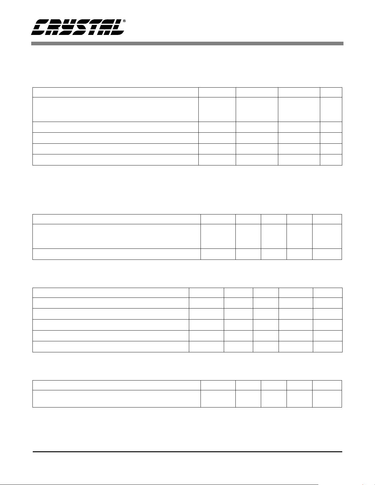
1. CHARACTERISTICS AND SPECIFICATIONS
ABSOLUTE MAXIMUM RATINGS
(AGND, DGND = 0 V; all voltages with respect to 0 V)
Parameter Symbol Min Max Unit
DC power supplies: Positive digital
Positive analog
||VA| – |VD||
Input current, any pin except supplies I
Digital input voltage V
Ambient operating temperature (power applied) T
Storage temperature T
WARNING: Operation at or beyond these limits may result in permanent damage to the device.
Normal operation is not guaranteed at these extremes.
RECOMMENDED OPERATING CONDITIONS
(AGND, DGND = 0 V; all voltages with respect to 0 V)
VD
VA
in
IND
Amax
stg
–0.3
–0.3
-
-
–0.3 5.5 V
–55 125
–65 150
3.63
3.63
0.4
±
10 mA
V
V
V
°
C
°
C
Parameter Symbol Min Typ Max Unit
DC power supplies: Positive digital
Positive analog
||VA| – |VD||
Ambient operating temperature T
VD
VA
3.13
3.13
-
A
0-70°C
3.3
3.3
-
DIGITAL D.C. CHARACTERISTICS
(TA = 25°C; VA, VD[3:1] = 3.3 V±5%; measurements performed under static conditions.)
Parameter Symbol Min Typ Max Unit
High-level input voltage V
Low-level input voltage V
High-level output voltage at I
Low-level output voltage at I
Input leakage current I
= –4.0 mA V
O
= 4.0 mA V
O
IH
IL
OH
OL
in
2.0 - - V
--0.8V
VD×0.9 - - V
--VD
--1.0µA
POWER SUPPLY CHARACTERISTICS
(TA = 25°C; VA, VD[3:1] = 3.3 V±5%; measurements performed under operating conditions)
Parameter Symbol Min Typ Max Unit
Power supply current: Digital operating: VD[3:1]
Analog operating: VA
-
-
225
4
3.47
3.47
0.4
×
0.1 V
435
8
V
V
V
mA
mA
4 DS262F2
CS4923/4/5/6/7/8/9
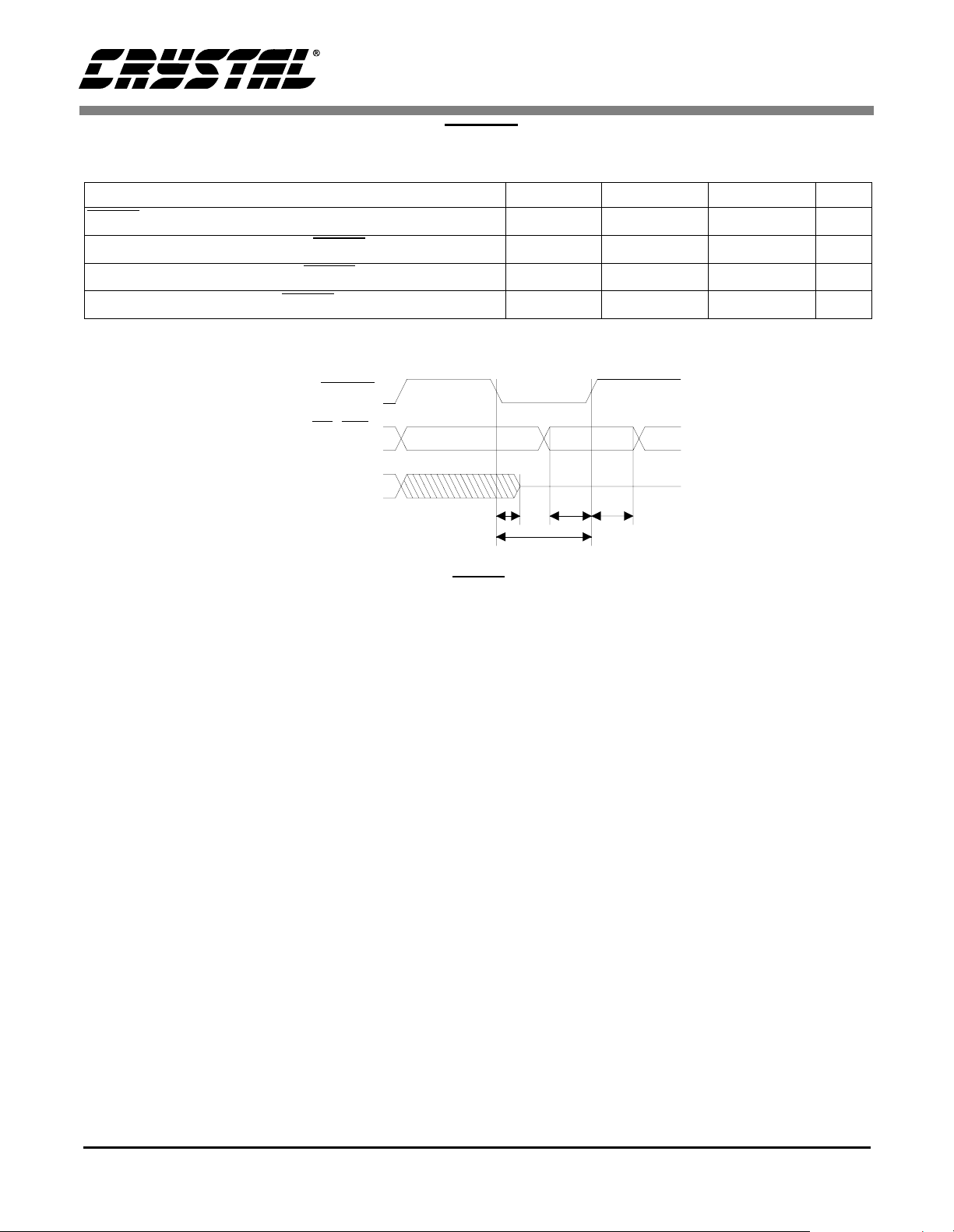
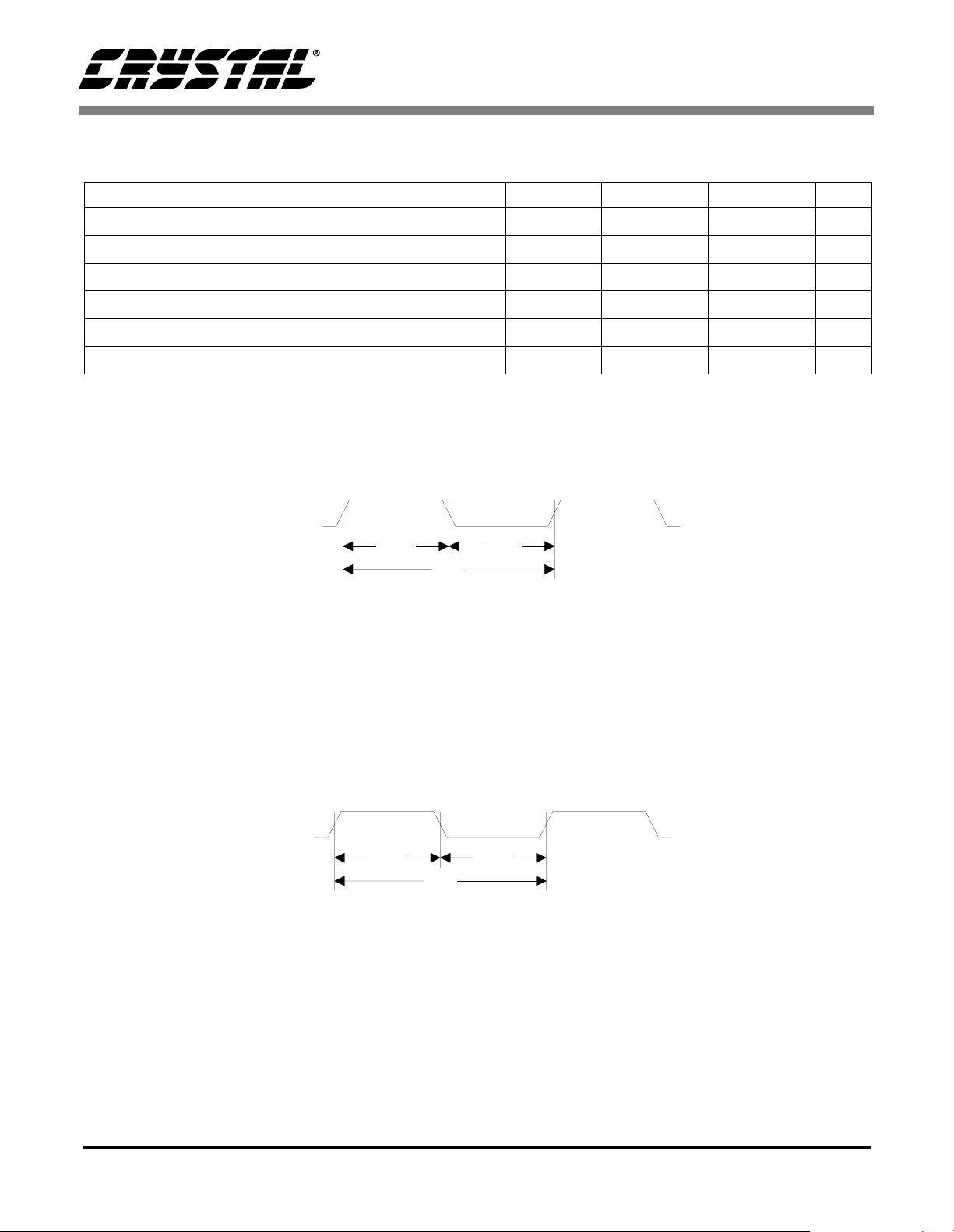
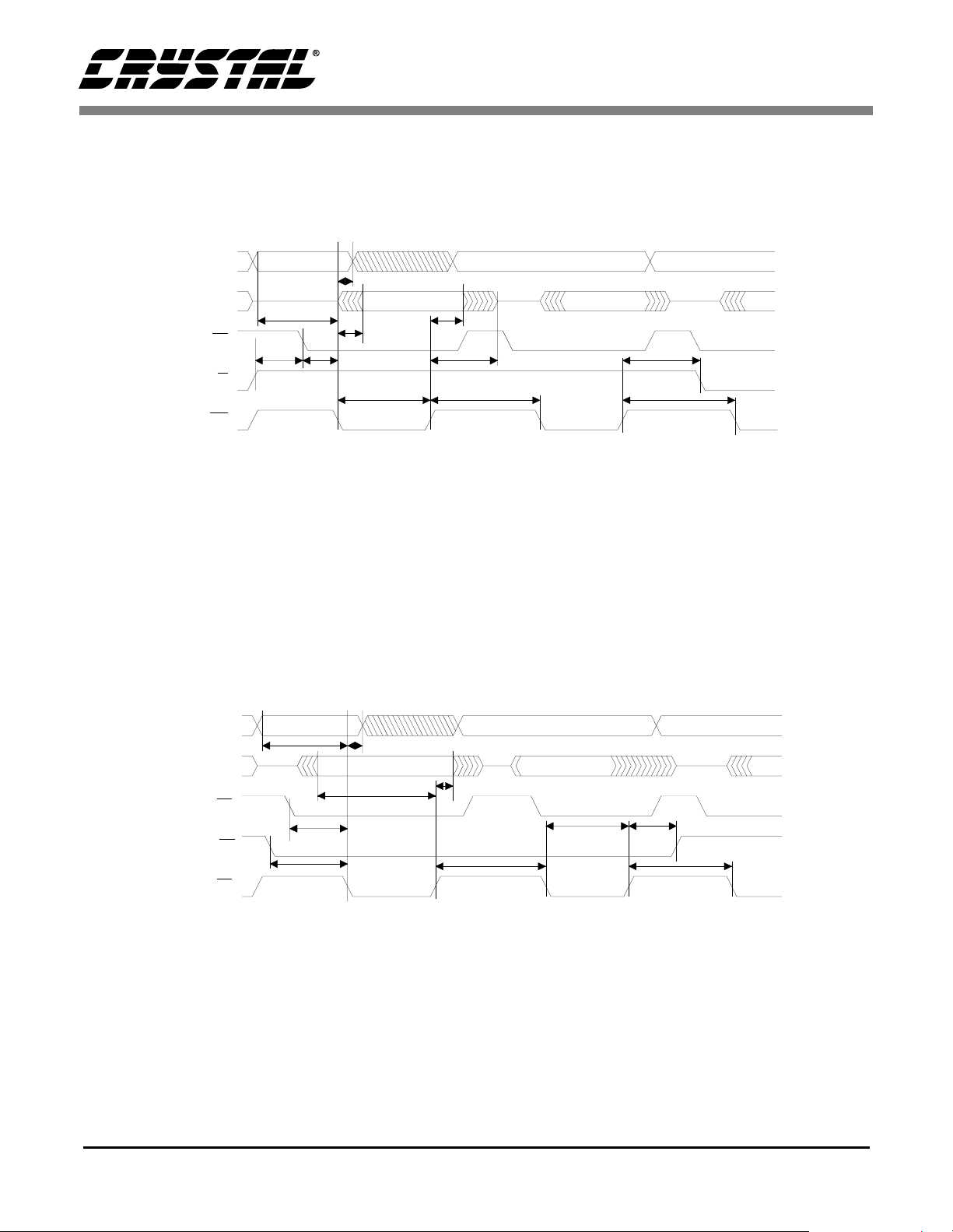
SWITCHING CHARACTERISTICS—RESET
(TA = 25°C; VA, VD = 3.3 V±5%; Inputs: Logic 0 = DGND, Logic 1 = VD, CL = 20 pF)z
Parameter Symbol Min Max Unit
RESET
minimum pulse width low
All bidirectional pins high-Z after RESET
Configuration bits setup before RESET
Configuration bits hold after RESET
high
RESET
RD, WR,
PSEL, ABOOT
All Bidirectional
Outputs
low
high
T
rst2z
T
rstl
T
T
T
T
rsthld
rstl
rst2z
rstsu
T
rstsuTrsthld
100 - ns
-50ns
50 - ns
15 - ns
Figure 1. RESET Timing
DS262F2 5
CS4923/4/5/6/7/8/9
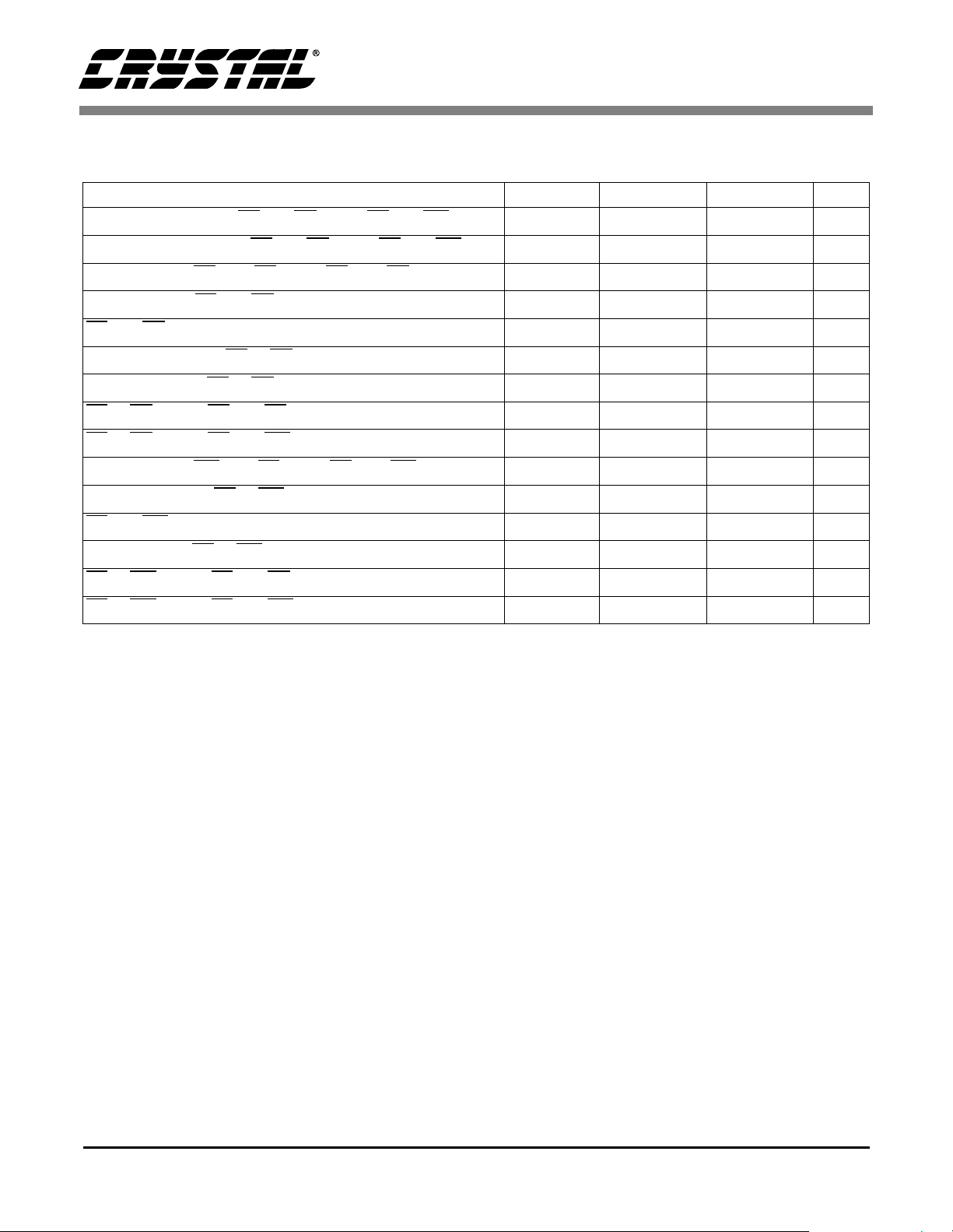
SWITCHING CHARACTERISTICS—CMPDAT, CMPCLK
(TA = 25°C; VA, VD = 3.3 V±5%; Inputs: Logic 0 = DGND, Logic 1 = VD, CL = 20 pF)
Parameter Symbol Min Max Unit
Serial compressed data clock CMPCLK period T
CMPDAT setup before CMPCLK high T
CMPDAT hold after CMPCLK high T
CMPCLK
CMPDAT
cmpclk
cmpsu
cmphld
37 - ns
5-ns
3-ns
T
cmpsu
T
cmpclk
T
cmphld
Figure 2. Serial Compressed Data Timing
6 DS262F2
CS4923/4/5/6/7/8/9
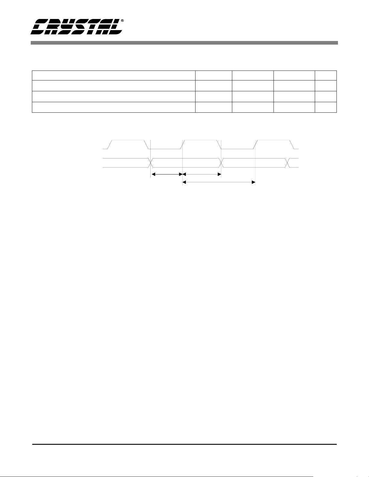
SWITCHING CHARACTERISTICS—CLKIN
(TA = 25°C; VA, VD = 3.3 V±5%; Inputs: Logic 0 = DGND, Logic 1 = VD, CL = 20 pF)
Parameter Symbol Min Max Unit
CLKIN period for internal DSP clock mode T
CLKIN high time for internal DSP clock mode T
CLKIN low time for internal DSP clock mode T
CLKIN period for external DSP clock mode T
CLKIN high time for external DSP clock mode T
CLKIN low time for external DSP clock mode T
CLKIN
clki
clkih
clkil
clke
clkeh
clkel
20 3800 ns
8ns
8ns
20 25 ns
9ns
9ns
T
clkih
T
clki
T
clkil
Figure 3. CLKIN with CLKSEL = VSS = PLL Enable
CLKIN
T
clkeh
T
Figure 4. CLKIN with CLKSEL = VD = PLL Bypass
clke
T
clkel
DS262F2 7
CS4923/4/5/6/7/8/9
SWITCHING CHARACTERISTICS—INTEL® HOST MODE
(TA = 25°C; VA, VD = 3.3 V±5%; Inputs: Logic 0 = DGND, Logic 1 = VD, CL = 20 pF)
Parameter Symbol Min Max Unit
Address setup before CS
Address hold time after CS
Delay between RD
Data valid after CS
and RD low for read (Note 1)
CS
Data hold time after CS
Data high-Z after CS
or RD high to CS and RD low for next read (Note 1)
CS
or RD high to CS and WR low for next write (Note 1)
CS
Delay bet ween WR
Data setup before CS
CS
and WR low for write (Note 1)
Data hold after CS
or WR high to CS and RD low for next read (Note 1)
CS
or WR high to CS and WR low for next write (Note 1)
CS
and RD low or CS and WR low
and RD low or CS and WR low
then CS low or CS then RD low
and RD low
or RD high
or RD high (Note 2)
then CS low or CS then WR low
or WR high
or WR high
T
T
T
T
T
T
T
T
T
T
T
T
T
T
ias
iah
icdr
idd
irpw
idhr
idis
T
ird
irdtw
icdw
idsu
iwpw
idhw
iwtrd
iwd
5-ns
5-ns
0
-20ns
DCLK + 10 - ns
5-ns
-15ns
2*DCLK + 10 - ns
2*DCLK + 10 - ns
0
20 - ns
DCLK + 10 - ns
5-ns
2*DCLK + 10 - ns
2*DCLK + 10 - ns
∞
∞
ns
ns
Notes: 1. Certain timing parameters are normalized to the DSP clock, DCLK, in nanoseconds. The DSP clock can
be defined as follows:
External CLKIN Mode:
DCLK == CLKIN/3 before and during boot
DCLK == CLKIN after boot
Internal Clock Mode:
DCLK == 10MHz before and during boot, i.e. DCLK == 100ns
DCLK == 60 MHz after boot, i.e. DCLK == 16.7ns (this speed may depend on CLKIN, please see
CS4923/4/5/6/7/8/9 Hardware User’s Guide for more information)
2. This specification is characterized but not production tested.
8 DS262F2
A1:0
DATA7:0
CS
WR
RD
CS4923/4/5/6/7/8/9
T
iah
T
ias
T
icdr
Figure 5. Intel Parallel Host Mode Read Cycle
T
idhr
T
idd
T
idis
T
irpw
T
ird
T
irdtw
A1:0
DATA7:0
CS
RD
WR
T
iah
T
ias
T
icdw
T
iwpw
T
idhw
T
idsu
T
iwd
T
iwtrd
Figure 6. Intel Parallel Host Mode Write Cycle
DS262F2 9
CS4923/4/5/6/7/8/9
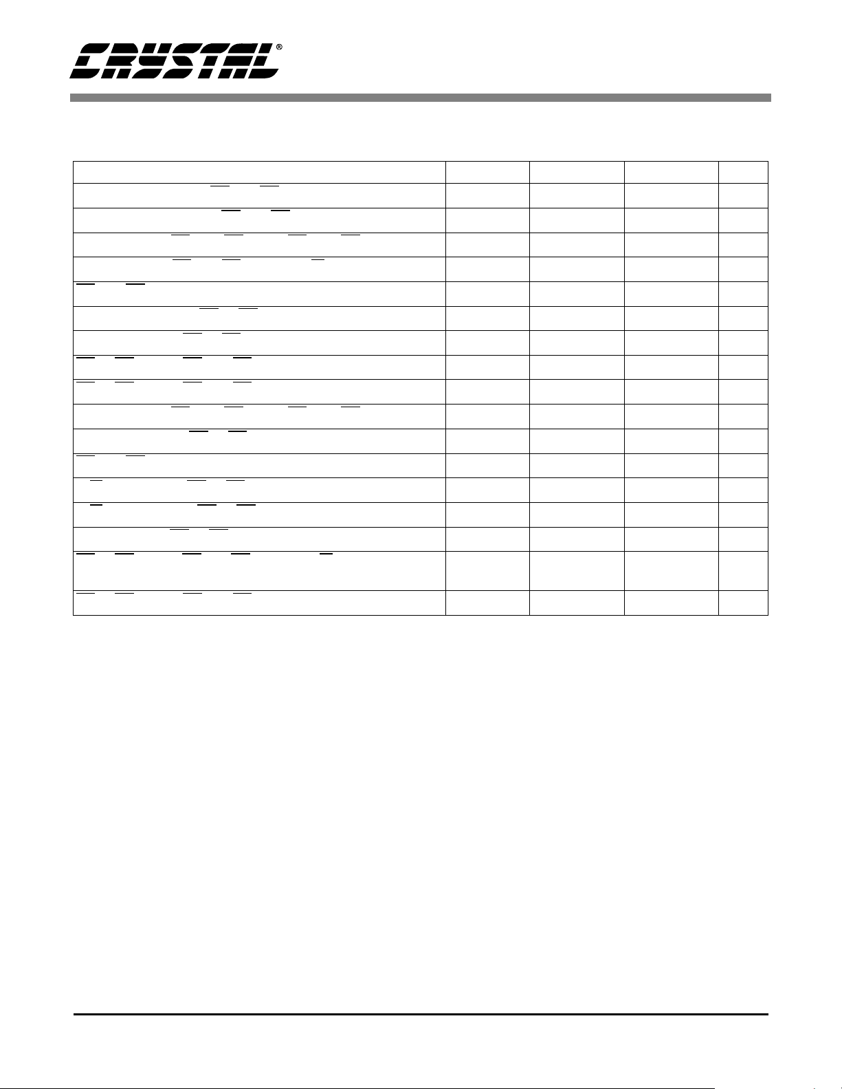
SWITCHING CHARACTERISTICS—MOTOROLA® HOST MODE
(TA = 25°C; VA, VD = 3.3 V±5%; Inputs: Logic 0 = DGND, Logic 1 = VD, CL = 20 pF)
Parameter Symbol Min Max Unit
Address setup before CS
Address hold time after CS
Delay between DS
Data valid after CS
and DS low for read (Note 3)
CS
Data hold time after CS
Data high-Z after CS
or DS high to CS and DS low for next read (Note 3)
CS
or DS high to CS and DS low for next write (Note 3)
CS
Delay between DS
Data setup before CS
CS
and DS low for write (Note 3)
setup before CS or DS low
R/W
hold time after CS or DS high
R/W
Data hold after CS
or DS high to CS and DS low with R/W high for next read
CS
and DS low
and DS low
then CS low or CS then DS low
and DS low with R/W high
or DS high after read
or DS high low after read (Note 4)
then CS low or CS then DS low
or DS high
or DS high
(Note 3)
CS
or DS high to CS and DS low for next write (Note 3)
T
mas
T
mah
T
mcdr
T
mdd
T
mrpw
T
mdhr
T
mdis
T
T
mrdtw
T
mcdw
T
mdsu
T
mwpw
T
mrwsu
T
mrwhld
T
mdhw
T
mwtrd
T
mwd
mrd
5-ns
5-ns
0
-20ns
DCLK + 10 - ns
5-ns
-15ns
2*DCLK + 10 - ns
2*DCLK + 10 - ns
0
20 - ns
DCLK + 10 - ns
5-ns
5-ns
5-ns
2*DCLK + 10 - ns
2*DCLK + 10 - ns
∞
∞
ns
ns
Notes: 3. Certain timing parameters are normalized to the DSP clock, DCLK, in nanoseconds. The DSP clock can
be defined as follows:
External CLKIN Mode:
DCLK == CLKIN/3 before and during boot
DCLK == CLKIN after boot
Internal Clock Mode:
DCLK == 10MHz before and during boot, i.e. DCLK == 100ns
DCLK == 60 MHz after boot, i.e. DCLK == 16.7ns (this speed may depend on CLKIN, please see
CS4923/4/5/6/7/8/9 Hardware Users Guide for more information)
4. This specification is characterized but not production tested.
10 DS262F2
A1:0
DATA7:0
CS
R/W
DS
T
mah
T
T
mrwsu
mas
T
mcdr
T
mdhr
T
mdd
T
mdis
T
mrpw
T
mrd
Figure 7. Motorola Parallel Host Mode Read Cycle
CS4923/4/5/6/7/8/9
T
mrwhld
T
mrdtw
A1:0
T
mas
T
mah
DATA7:0
T
mdsu
T
mdhw
CS
T
T
mcdw
T
mwpw
mrwhld
R/W
T
mrwsu
T
mwd
T
mwtrd
DS
Figure 8. Motorola Parallel Host Mode Write Cycle
DS262F2 11
CS4923/4/5/6/7/8/9
SWITCHING CHARACTERISTICS—SPI CONTROL PORT
(TA = 25°C; VA, VD = 3.3 V±5%; Inputs: Logic 0 = DGND, Logic 1 = VD, CL = 20 pF)
Parameter Symbol Min Max Units
SCCLK clock frequency (Note 5) f
falling to SCCLK rising t
CS
Rise time of SCCLK line (Note 11) t
Fall time of SCCLK lines (Note 11) t
SCCLK low time t
SCCLK high time t
Setup time SCDIN to SCCLK rising t
Hold time SCCLK rising to SCDIN (Note 6) t
Transition time from SCCLK to SCDOUT valid (Note 7) t
Time from SCCLK rising to INTREQ
Rise time for INTREQ
Hold time for INTREQ
from SCCLK rising (Note 9, 11) t
Time from SCCLK falling to CS
rising (Note 8) t
(Note 8) t
rising t
High time between active CS
Tim e from CS
rising to SCDOUT high-Z (Note 11) t
sck
css
r
f
scl
sch
cdisu
cdih
scdov
scrh
rr
scrl
sccsh
t
csht
cscdo
-2000kHz
20 - ns
-50ns
-50ns
150 - ns
150 - ns
50 - ns
50 - ns
-40ns
-200ns
-(Note
ns
10)
0-ns
20 - ns
200 - ns
10 ns
Notes: 5. The specification f
aware that the actual maximum speed of the communication port may be limited by the software. The
relevant application code user’s manual should be consulted for the software speed limitations.
6. Data must be held for sufficient time to bridge the 50 ns transition time of SCCLK.
7. SCDOU T sh oul d
8. INTREQ
goes high only if there is no data to be read from the DSP at the rising edge of SCCLK for the
second-to-last bit of the last byte of data during a read operation as shown.
9. If INTREQ
goes high as indicated in Note 8, then INTREQ is guaranteed to remain high until the next
rising edge of SCCLK. If there is more data to be read at this time, INTREQ
this condition as a new read transaction. Raise chip select to end the current read transaction and then
drop it, followed by the 7-bit address and the R/W
10. With a 4.7k Ohm pull-up resistor this value is typically 215ns. As this pin is open drain adjusting the pull
up value will affect the rise time.
11. This time is by design and not tested.
indicates the maximum speed of the hardware. The system designer should be
sck
not
be sampled during this time period.
goes active low again. Treat
bit (set to 1 for a read) to start a new read transaction.
12 DS262F2
DS262F2 13
t
sccsh
CS
SCCLK
SCDIN
SCDOUT
INTR EQ
t
css
t
t
cscdo
csht
A6
tri-state
t
scl
t
cdisu
1
t
sch
t
cdih
2
6
A0A6 A5
7
R/W
t
scdov
0
MSB
MSB
t
scdov
t
scrh
6
LSB
LSB
t
scrl
7
5
0
t
t
r
f
CS4923/4/5/6/7/8/9
Figure 9. SPI Control Port Timing

CS4923/4/5/6/7/8/9
SWITCHING CHARACTERISTICS— I2C® CONTROL PORT
(TA = 25°C; VA, VD = 3.3 V±5%; Inputs: Logic 0 = DGND, Logic 1 = VD, CL = 20 pF)
Parameter Symbol Min Max Units
SCCLK clock frequency (Note 12) f
Bus free time between transmissions t
Start-condition hold time (prior to first clock pulse) t
Clock low time t
Clock high time t
SCDIO setup time to SCCLK rising t
SCDIO hold time from SCCLK falling (Note 13) t
Rise time of SCCLK (Note 14), (Note 18) t
Fall time of SCCLK (Note 18) t
Time from SCCLK falling to CS4923/4/5/6/7/8/9 ACK t
Time from SCCLK falling to SCDIO valid during read operation t
Time from SCCLK rising to INTREQ
Hold time for INTREQ
from SCCLK rising (Note 16) t
rising (Note 15) t
Rise time for INTREQ
Setup time for stop condition t
scl
buf
hdst
low
high
sud
hdd
r
f
sca
scsdv
scrh
scrl
t
rr
susp
400 kHz
4.7
4.0
1.2
1.0
µ
s
µ
s
µ
s
µ
s
250 ns
0
µ
s
50 ns
300 ns
40 ns
40 ns
200 ns
0ns
(Note
ns
17)
4.7
µ
s
Notes: 12. The specification f
aware that the actual maximum speed of the communication port may be limited by the software. The
relevant application code user’s manual should be consulted for the software speed limitations.
13. Data must be held for sufficient time to bridge the 300-ns transition time of SCCLK. This hold time is by
design and not tested.
14. This rise time is shorter than that recommended by the I
section on SCP communications.
15. INTREQ
goes high only if there is no data to be read from the DSP at the rising edge of SCCLK for the
last data bit of the last byte of data during a read operation as shown.
16. If INTREQ
goes high as indicated in Note 8, then INTREQ is guaranteed to remain high until the next
rising edge of SCCLK. If there is more data to be read at this time, INTREQ
this condition as a new read transaction. Send a new start condition followed by the 7-bit address and
the R/W
bit (set to 1 for a read). This time is by design and is not tested.
17. With a 4.7k Ohm pull-up resistor this value is typically 215ns. As this pin is open drain adjusting the pull
up value will affect the rise time.
18. This time is by design and not tested.
indicates the maximum speed of the hardware. The system designer should be
scl
2
C specifications. For more information, see the
goes active low again. Treat
14 DS262F2
DS262F2 15
SCDIO
SCCLK
INTREQ
stop start
t
buf
t
hdst
t
t
low
sud
0
t
hddthigh
16
t
rtf
Figure 10. I2C Control Port Timing
t
scsdv
MSBA0A6 A5
t
ACK
sca
R/W
780
t
scrh
LSB
7
ACK
t
scrl
stop
8
t
susp
CS4923/4/5/6/7/8/9

CS4923/4/5/6/7/8/9
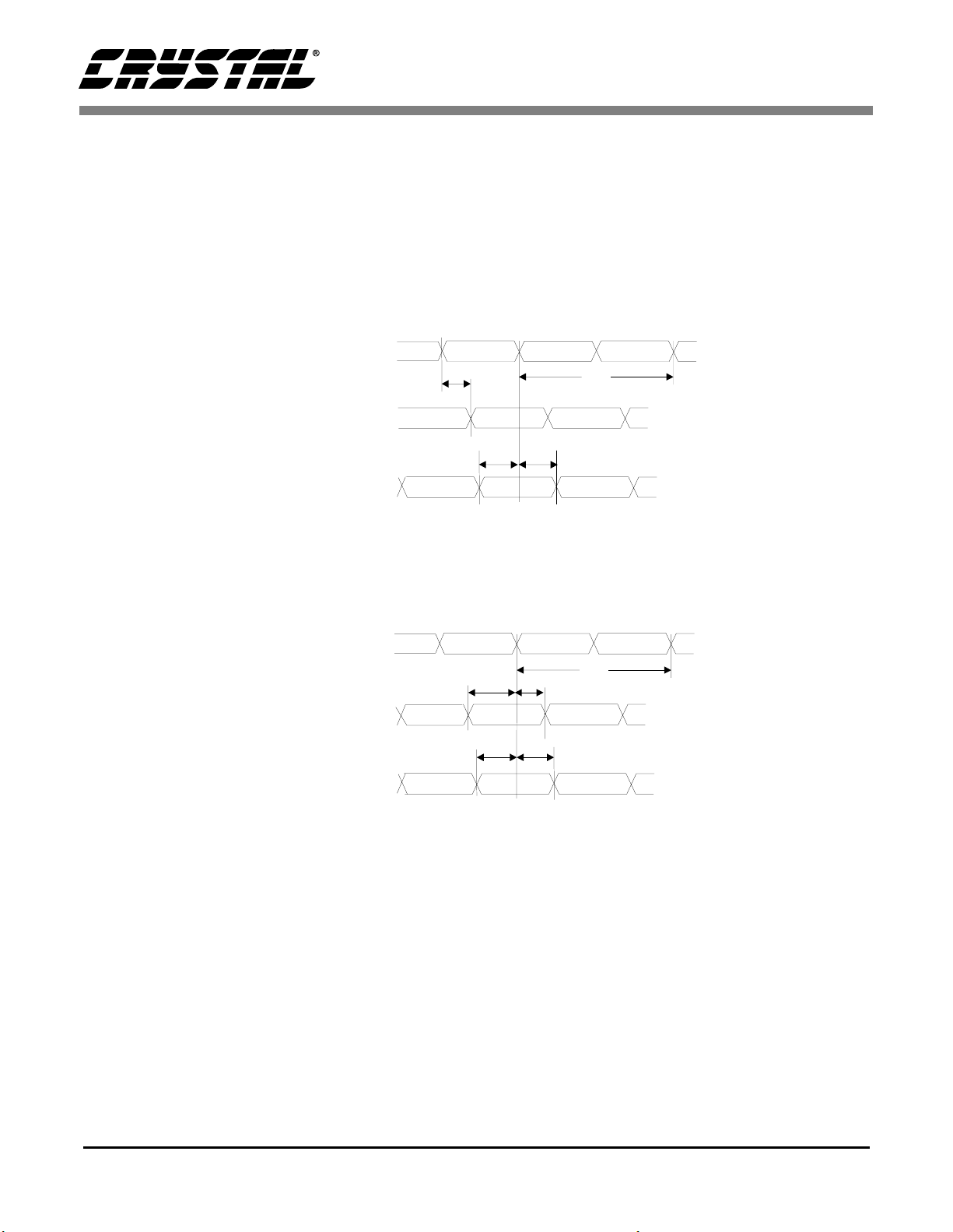
SWITCHING CHARACTERISTICS—DIGITAL AUDIO INPUT
(TA = 25°C; VA, VD = 3.3 V±5%; Inputs: Logic 0 = DGND, Logic 1 = VD, CL = 20 pF)
Parameter Symbol Min Max Unit
SCLKN1(2) period for both Master and Slave mode (Note 19) T
sclki
SCLKN1(2) duty cycle for Master and Slave mode (Note 19) 45 55 %
Master Mode (Note 19,20)
LRCLKN1(2) delay after SCLKN1(2) transition (Note 21) T
SDATAN1(2) setup to SCLKN1(2) transition (Note 22) T
SDATAN1(2) hold time after SCLKN1(2) transition (Note 22) T
lrds
sdsum
sdhm
Slave Mode (Note 23)
Time from active edge of SCLKN1(2) to LRCLKN1(2) transition T
Time from LRCLKN1(2) transition to SCLKN1(2) active edge T
SDATAN1(2) setup to SCLKN1(2) transition (Note 22) T
SDATAN1(2) hold time after SCLKN1(2) transition (Note 22) T
stlr
lrts
sdsus
sdhs
Notes: 19. Master mode timing specifications are characterized, not production tested.
20. Master mode is defined as the CS4923 driving LRCLKN1(2) and SCLKN1(2). Master or Slave mode
can be programmed.
21. This timing parameter is defined from the non-active edge of SCLKN1(2). The active edge of
SCLKN1(2) is the point at which the data is valid.
22. This timing parameter is defined from the active edge of SCLKN1(2). The active edge of SCLKN1(2) is
the point at which the data is valid.
23. Slave mode is defined as SCLKN1(2) and LRCLKN1(2) being driven by an external source.
40 - ns
-10ns
10 - ns
5-ns
10 - ns
10 - ns
5-ns
5-ns
16 DS262F2
SCLKN1
SCLKN2
LRCLKN1
LRCLKN2
SDATAN1
SDATAN2
MASTER MODE
T
lrds
T
sdsumTsdhm
CS4923/4/5/6/7/8/9
T
sclki
SLAVE MODE
SCLKN1
SCLKN2
T
T
lrts
LRCLKN1
LRCLKN2
T
sdsus
T
sdhs
SDATAN1
SDATAN2
Figure 11. Digital Audio Input, Data and Clock Timing
sclki
T
stlr
DS262F2 17
CS4923/4/5/6/7/8/9
SWITCHING CHARACTERISTICS—DIGITAL AUDIO OUTPUT
(TA = 25°C; VA, VD = 3.3 V±5%; measurements performed under static conditions.)
Parameter Symbol Min Max Unit
MCLK period (Note 24) T
mclk
MCLK duty cycle (Note 24) 40 60 %
SCLK period for Master or Slave mode (Note 25) T
sclk
SCLK duty cycle for Master or Slave mode (Note 25) 45 55 %
Master Mode (Note 25,26)
SCLK delay from MCLK rising edge, MCLK as an input T
SCLK delay from MCLK rising edge, MCLK as an output T
LRCLK delay from SCLK transition (Note 27) T
AUDATA2–0 delay from SCLK transition (Note 27) T
sdmi
sdmo
lrds
adsm
Slave Mode (Note 28)
Time from active edge of SCLKN1(2) to LRCLKN1(2) transition T
Time from LRCLKN1(2) transition to SCLKN1(2) active edge T
AUDATA2–0 delay from SCLK transition (Note 27,29) T
stlr
lrts
adss
40 - ns
40 - ns
15 ns
–5 10 ns
10 ns
10 ns
10 - ns
10 - ns
15 ns
Notes: 24. MCLK can be an input or an output. These specifications apply for both cases.
25. Master mode timing specifications are characterized, not production tested.
26. Master mode is defined as the CS4923 driving both SCLK and LRCLK. When MCLK is an input, it is
divided to produce SCLK and LRCLK.
27. This timing parameter is defined from the non-active edge of SCLK. The active edge of SCLK is the
point at which the data is valid.
28. Slave mode is defined as SCLK and LRCLK being driven by an external source.
29. This specification is characterized, not production tested.
18 DS262F2

MCLK (Input)
SCLK (Output)
MCLK (Output)
SCLK (Output)
SCLK
LRCLK
T
sdmi
T
sdmo
MASTER MODE
T
sclk
T
lrds
CS4923/4/5/6/7/8/9
T
mclk
T
mclk
T
adsm
AUDATA2:0
SLAVE MODE
SCLK
T
T
lrts
LRCLK
T
adss
AUDATA2:0
Figure 12. Digital Audio Output, Data an d Clock Timing
sclk
T
stlr
DS262F2 19
CS4923/4/5/6/7/8/9
2. FAMILY OVERVIEW
The CS4923, CS4924, CS4925, CS4926, CS4927,
CS4928 and the CS4929 are system on a chip
solutions for multi-channel (or stereo in the case of
the CS4929) audio decompression and digital
signal processing. Because the parts are primarily
RAM-based, a download of application software is
required each time the CS4923/4/5/6/7/8/9 is
powered up. This document uses “download” and
“code load” interchangeably. These terms should
be interpreted as meaning the transfer of
application code into the internal
CS4923/4/5/6/7/8/9 memory from either an
external microcontroller or through the autoboot
procedure.
This document focuses on the electrical features
and characteristics of these parts. The different
features are described from a hardware design
perspective. It should be understood that not all of
the features portrayed in this document are
supported by all of the versions of application code
available. The application user’s guides (see
section 2.2.2) should be consulted to confirm
which hardware features are supported by the
software. This document will be valuable to both
the hardware designer and the system programmer.
This data sheet covers the CS4923, CS4924,
CS4925, CS4926, CS4927, CS4928 and CS4929.
These parts are identical from an external electrical
perspective. Internally each device has been
tailored for supporting different decoding
standards. For this document CS4923/4/5/6/7/8/9
has been replaced in certain places with CS492X
for readability. Unless otherwise specified
CS492X should be interpreted as applying to the
CS4923, CS4924, CS4925, CS4926, CS4927,
CS4928 and CS4929.
There are two revisions of silicon commercially
available. The features available on Revision D are
a super-set of those features available on Revision
B. Differences between the revisions are pointed
out when features are discussed within this
document. The silicon revision for any chip can be
determined by referencing Table 1 below.
Revision B Revision D
CS492301 CS492305
CS492401 CS492405
CS492501 CS492505
CS492603 CS492604
CS492705
CS492804
CS492906
Table 1 . Silicon Revisions
These parts are generally targeted at two different
market segments. The broadcast market where
audio/video (A/V) synchronization is required, and
the outboard decoder markets where audio/video
synchronization is not required. The important
differentiation is the format in which the data will
be received by the CS4923/4/5/6/7/8/9. In systems
where A/V synchronization is required from the
CS4923/4/5/6/7/8/9, the incoming data is typically
PES encoded. In an outboard decoder application
the data typically comes in the IEC61937 format
(as specified by the DVD consortium). An
important point to remember is that the
CS4923/4/5/6/7/8/9 will support both
environments, but different downloads are required
depending on the input data type.
Broadcast applications include (but are not limited
to) set top box applications, DVDs and digital TVs.
Outboard decoder applications include standalone
decoders and audio/video receivers. Often times a
system may be a hybrid between an outboard
decoder and a broadcast system depending on its
functionality.
As discussed above, compressed audio can be
packed in IEC61937, PES, or elementary formats
depending on the decoder environment. Each format is supported by a separate download of application code. Consult the relevant Application Code
20 DS262F2

CS4923/4/5/6/7/8/9
User’s Guide to determine which format s are supported by a particular application. A brief description of each format is presented below.
Elementary - an elementary bitstream consists only
of compressed audio data (e.g., strictly the Dolby
Digital bitstream); used primarily in broa dcast environments.
PES - a Packetized Elementary Stream (PES) bitstream contains the elementary compr essed audio
stream and additional header information which
can be used for A/V synchronization; used primarily in broadcast environments.
IEC61937 - a method of packing compressed audio
such that it can be delivered using a bi-phase encoded signal (e.g., S/PDIF output signal from DVD
player); used primarily for outboard decoders
where A/V synchronization is not required.
2.1 Multi-channel Decoder Family of Parts
CS4923 - Dolby Digital
CS4923 is the original member of the family and is
intended to be used if only Dolby Digital decoding
is required. For Dolby Digital, post processing
includes bass management, delays and Dolby Pro
Logic decoding. Separate downloads can also be
used to support stereo to 5.1 channel effects
processing and stereo MPEG decoding.
CS4924 - Dolby Digital
Decoder. The CS4924 is the stereo version of the
CS4923 designed for source products such as
DVD, HDTV, and set-top boxes. Separate
downloads are available for stereo decode of Dolby
Digital and MPEG audio.
CS4925 - International Multi-Channel DVD
Audio Decoder. The CS4925 supports both Dolby
Digital and MPEG-2 multi-channel formats. For
both Dolby Digital and MPEG-2 multi-channel,
post processing includes bass management and
Dolby Pro Logic decoding. Separate downloads are
available for decode of Dolby Digital and MPEG
TM
Audio Decoder. The
TM
Source Product
audio. Another code load can be used to support
stereo to 5.1 channel effects processing.
CS4926 - DTS/Dolby® Multi-Channel Audio
Decoder. The CS4926 supports both Dolby Digital
and DTS, or Digital Theater Surround. For Dolby
Digital, post processing includes bass management
and Dolby Pro Logic. The Dolby Digital code and
DTS code take separate code downloads. Separate
downloads can also be used to support stereo to 5.1
channel effects processing and stereo MPEG
decoding.
CS4927 - MPEG-2 Multi-Channel Decoder. The
CS4927 supports MPEG-2 multi-channel decoding
and should be used in applications where Dolby
Digital decoding is not necessary. For MPEG-2
multi-channel decoding, post processing includes
bass management and Dolby Pro Logic decoding.
Another code load can be used to support stereo to
5.1 channel effects processing.
CS4928 - DTS Multi-Channel Decoder. The
CS4928 supports DTS multi-channel decoding and
should be used in applications where Dolby Digital
decoding is not necessary. For DTS multi-channel
decoding, post processing includes bass
management. Separate downloads can also be used
to support stereo to 5.1 channel effects processing
and stereo MPEG decoding.
CS4929 - AAC 2-Channel, (Low Complexity) and
MPEG-2 Stereo Decoder. The CS4929 is capable
of decoding both 2-channel AAC and MPEG-2
audio. The CS4929 supports elementary and PES
formats.
2.2 Document Strategy
Multiple documents are needed to fully define,
understand and implement the functionality of the
CS4923/4/5/6/7/8/9. They can be split up into two
basic groups: hardware and application code
documentation. It should be noted that hardware
and application code are co-dependent and one can
not successfully use the device without an
DS262F2 21

CS4923/4/5/6/7/8/9
understanding of both. The ‘ANXXX’ notation
denotes the application note number under which
the respective user’s guide was released.
2.2.1 Hardware Documentation
CS4923/4/5/6/7/8/9 Family Data Sheet - This
document describes the el ec tric al char acte ristic s of
the device from timing to base functionality. This is
the hardware designers tool to learn the part’s
electrical and systems requirements.
AN115 - CS4923/4/5/6/7/8/9 Hardware User’s
Guide - describes the functional aspects of the
device. An in depth description of communication,
boot procedure, external memory and hardware
configuration are given in this document. This
document will be valuable to both the hardware
designer and the system programmer.
2.2.2 CS4923/4/5/6/7/8/9 Application Code
User’s Guides
The following application notes describe the
application codes used with the
CS4923/4/5/6/7/8/9. Whenever an application code
user’s guide is referred to, it should be assumed that
one or more of the below documents are being
referenced. The following list covers currently
released application notes. This list will grow with
each new application released. For a current list of
released user’s guides please see www.crystal.com
and search for the part number.
AN120 - Dolby Digital User’s Guide for the
CS4923/4/5/6. This document covers the features
available in the Dolby Digital code including
delays, pink noise, bass management, Pro Logic,
PCM pass through and Dolby Digital processing
features. Optional appendices are available that
document code for Dolby Virtual, Q-Surround and
VMAx.
AN121 - MPEG User’s Guide for the CS4925.
This document covers the features available in the
MPEG Multi-Channel code including delays, bass
management, Pro Logic, and MPEG processing
features.
AN122 - DTS User’s Guide for the CS4926,
CS4928. This document covers the features
available in the DTS code including bass
management and DTS processing features.
AN123 - Surround User’s Guide for the
CS4923/4/5/6/7/8. This code covers the different
Stereo PCM to surround effects processing code.
Optional appendices are available that document
Crystal Original Surround, Circle Surround and
Logic 7.
AN140 - Broadcast Systems Guide for the
CS4923/4/5/6/7/8/9. This guide describes all
application code (e.g. Dolby Digital, MPEG, AAC)
designed for broadcast systems such as HDTV and
set-top box receivers. This document also provides
a discussion of broadcast system considerations
and dependencies such as A/V synchronization and
channel change procedures.
2.3 Using the CS4923/4/5/6/7/8/9
No matter what application is being used on the
chip, the following four steps are always followed
to use the CS4923/4/5/6/7/8/9 in system.
1) Reset and/or Download Code - Detailed
information in AN115
2) Hardware Configuration - Detailed information
in AN115
3) Application configuration - Detailed
information in the appropriate Application
Code User’s guide
4) Kickstart - This is the “Go” command to the
CS492X once the system is properly
configured. Information can be found in the
appropriate Application Code User’s guide.
22 DS262F2

CS4923/4/5/6/7/8/9
3. TYPICAL CONNECTION DIAGRAMS
Six typical connection diagrams have been
presented to illustrate using the device with the
different communication modes available. They
are as follows:
Figure 13: I2C Control
Figure 14: I2C Control with External Memory
Figure 15: SPI Control
Figure 16: SPI Control with External Memory
Figure 17: Intel Parallel Control Mode
Figure 18: Motorola Parallel Control Mode
The following should be noted when viewing the
typical connection diagrams:
The pins are grouped functionally in each of the
typical connection diagrams. Please be aware that
the CS4923/4/5/6/7/8/9 symbol may appear
differently in each diagram.
The external memory interface is only supported
when a serial communication mode has been
chosen.
The typical connection diagrams demonstrate the
PLL being used (CLKSEL is pulled low). To
enable external CLKIN, CLKSEL should be pulled
high. The system designer must be aware that
certain software features may not be available if
external CLKIN is used as the DSP must run
slower when external CLKIN is use d. The system
designer should also be aware of additional duty
cycle requirements when using external CLKIN
mode. It is highly suggested that the system
designer take advantage of the PLL and pull
CLKSEL low.
3.1 Multiplexed Pins
The CS4923/4/5/6/7/8/9 family of digital signal
processors (DSPs) incorporate a large amount of
flexibility into a 44 pin package. Because of the
high degree of integration, many of these pins are
internally multiplexed to serve multiple purposes.
Some pins are designed to operate in one mode at
power up, and serve a different purpose when the
DSP is running. Other pins have functionality
which can be controlled by the application running
on the DSP. In order to better explain the behavior
of the part, the pins which are multiplexed have
been given multiple names. Each name is specific
to the pin’s operation in a particular mode.
An example of this would be the use of pin 20 in
one of the serial control modes. During the boot
period of the CS492X, pin 20 is called ABOOT.
ABOOT is sampled on the rising edge of RESET.
If ABOOT is high the host must download code to
the DSP. If ABOOT is low when sampled, the
CS492X goes into autoboot mode and loads itself
with code by generating addresses and reading data
on EMAD[7:0]. When the device has been loaded
with code and is running an application, however,
pin 20 is called INTREQ. INTREQ is an open drain
output used to inform the host that the DSP has an
outgoing message which should be read.
In this document, pins will be referred to by their
functionality. The section “Pin Descriptions” on
page 49 describes each pin of the CS492X and lists
all of its names. Please refer to the Pin Descriptions
section when exact pin numbers are in question.
The device has 12 general purpose input and output
(GPIO[11:0]) pins that all have multiple
functionality. While in one of the parallel
communication modes (see section 6.2), these pins
are used to implement the parallel host
communication interface. While in one of the serial
host modes these pins are used to implement an
external memory interface. Alternatively while in
one of the serial host modes these pins could be
used for another general purpose if the application
code has been programmed to support the special
purpose. In this document the pins are referenced
by the name corresponding to their particular use.
Sometimes GPIO[11:0], or some subset thereof, is
used when referring to the pins in a general sense.
DS262F2 23

CS4923/4/5/6/7/8/9
3.2 Termination Requirements
The CS4923/4/5/6/7/8/9 incorporates open drain
pins which must be pulled high for proper
operation. INTREQ (pin 20) is always an open
drain pin which requires a pull-up for proper
operation. When in the I2C serial communication
mode, the SCDIO signal (pin 19) is open drain and
thus requires a pull-up for proper operation.
Due to the internal, multiplexed design of the pins,
certain signals may or may not require termination
depending on the mode being used. If a parallel
host communication mode is not being used,
GPIO[11:0] must be terminated or driven as these
pins will come up as high impedance inputs and
will be prone to oscillation if they are left floating.
The specific termination requirements may vary
since the state of some of the GPIO pins will
determine the communication mode at the rising
edge of reset (please see section 6 for more
information). For the explicit termination
requirements of each communication mode please
see the typical connection diagrams.
Generally a 4.7k Ohm resistor is recommended for
open drain pins while a 10k Ohm resistor is
sufficient for the GPIO pins and unused inputs.
3.3 Phase Locked Loop Filter
The internal phase locked loop (PLL) of the
CS4923/4/5/6/7/8/9 requires an external filter for
successful operation. The topology of this filter and
component values are shown in the typical
connection diagrams. Care should be taken when
laying out the filter circuitry to minimize trace
lengths and to avoid any close routing of high
frequency signals. Any noise coupled on to the
filter circuit will be directly coupled into the PLL,
which could affect performance.
24 DS262F2
+3.3V Supply (+3.3VD)
NOTE: A capacitor pair (1 uF and 0.1 uF) must be supplied for each power pin.
NOTE: +3.3VA is simply +3.3VD after fil tering through the ferrite bead. Pin 32 must be referenced to +3.3VA
1 uF 0.1 uF
+
10k
Resistor Pack 10k
I2C INTERFACE
MICROCONTROLLER
10k
0.1 uF
1 uF 0.1 uF
+
10k
10k
4.70K
EMAD_GPIO [8:0]
CS4923/4/5/6/7/8/9
FERRITE BEAD
1 uF
+
1 uF 0.1 uF
+
+3.3VD+3.3VD
4.70K
4.70K
4.70K
37
DD
38
DC
20
INTREQ
19
SCDIO
6
SCDIN
18
CS
7
SCCLK
36
RESET
1
12
23
VD1
VD2
VD3
CS4923/4/5/6/7/8/9
4
WR__GPIO10
5
RD__GPIO11
21
GPIO8
8
GPIO7
9
GPIO6
10
GPIO5
11
GPIO4
14
GPIO3
15
GPIO2
16
GPIO1
17
GPIO0
DGND1
2
DGND2
13
DGND3
24
AGND
35
+3.3VA
47 uF
+
NOTE: Only AUDATA0 connection applies for the CS4929
34
VA
MCLK
SCLK
LRCLK
AU D ATA 0
AU D ATA 1
AU D ATA 2
CMPDAT
CMPCLK
CMPREQ
SD ATA N
SCLKN
SLRCLKN
XMT958
CLKIN
CLKSEL
FLT2
FLT1
0.22 uF
44
43
42
41
40
39
27
28
29
22
25
26
3
30
31
32
33
33
33
+3.3VA
2.2 uF
+
33
DAC (S)
DIR or
ADC [S]
OPT_TX
OSCILLATOR
10k
2
Figure 13. I
C Control
DS262F2 25

CS4923/4/5/6/7/8/9
NOTE: A capacitor pair (1 uF
and 0.1 uF) must be supplied for each power pin.
SYS
TEM
MICRO
CONTROL
LER
I2C INTERFACE
D[7:0]Q[7:0]
D[7:
0]
Q[7:0]
OCTAL F/
F
OCTAL F/
F
EXTERNAL
ROM
A[7:0
]
A[15:8]
D[7:0]/CE
/O
E
DIR orADCs
DACs
OSCILL
ATOR
NOTE: +3.3VA is simply +3.3VD after filt
ering through the ferrite bead. Pin 32 must be referenced to +3.3VA
EMAD[7:0
]
+3.3V Supply (+3.3VD)
+3.3VD
+3.3VD
+3.3VA
+3.3VA
0.1 uF+1 uF
0.1 uF+1 uF
0.1 uF+1 uF+1 uF
0.1 uF
4.70K
4.70K
4.70K
10 k
10k
Resistor Pack 10k
10k
FERRITE BEAD
10k
4.70K
10 k
33
OPT_T
X
33
33+2.2 uF
0.22 uF+47 uF
10k
CS4923/4/5/6/7/8/9
1
2
34567891011
12
13
141516
1718192021
22
23
24
252627282930313233
34
35
36
373839
40
41
42
43
44
VD1
DGND1
XMT958
WR__GPIO10
RD__EMOE
SCDIN
SCCLK
EMAD7
EMAD6
EMAD5
EMAD4
VD2
DGND2
EMAD3
EMAD2
EMAD1
EMAD0
CS
SCDIO
INTREQ__ABOOT
EXTMEM
SDATA N
VD3
DGND3
SCLKN
SLRCLKN
CMPDAT
CMPCLK
CMPREQ
CLKIN
CLKSEL
FLT2
FLT1
VA
AGND
RESET
DD
DC
AUD ATA2
AUD ATA1
AUD ATA0
LRCLK
SCLK
MCLK
NOTE: Only AUDATA0 connection applies for the CS4929
26 DS262F2
Figure 14. I2C Control with External Memory

+3.3V Supply (+3.3VD)
NOTE: A capacitor pair (1 uF and 0.1 uF) must be supplied for each power pin.
NOTE: +3.3VA is simply +3.3VD after filt ering through the ferrite bead. Pin 32 must be referenced to +3.3VA
0.1 uF
1 uF 0.1 uF
+
1 uF 0.1 uF
+
1 uF
+
FERRITE BEAD
1 uF 0.1 uF
+
+
CS4923/4/5/6/7/8/9
+3.3VA
47 uF
SPI INTERFACE
MICROCONTROLLER
+3.3VD
Resistor Pack 10k
EMAD_GPIO [8:0]
10k
+3.3VD
10 k
10k
4.70K
4.70K
4.70K
1
12
23
37
38
20
19
6
18
7
36
DD
DC
INTREQ
SCDOUT
SCDIN
CS
SCCLK
RESET
VD3
VD2
VD1
CS4923/4/5/6/7/8/9
5
RD__GPIO11
4
WR__GPIO10
21
GPIO8
8
GPIO7
9
GPIO6
10
GPIO5
11
GPIO4
14
GPIO3
15
GPIO2
16
GPIO1
17
GPIO0
DGND1
2
DGND2
13
NOTE: Only AUDATA0 connection applies for the CS4929
DGND3
24
35
AGND
34
VA
MCLK
SCLK
LRCLK
AU D ATA0
AU D ATA1
AU D ATA2
CMPDAT
CMPCLK
CMPREQ
SD ATA N
SCLKN
SLRCLKN
XMT958
CLKIN
CLKSEL
FLT2
FLT1
0.22 uF
33
44
33
43
42
41
40
39
27
28
29
22
25
26
3
+3.3VA
2.2 uF
+
33
30
31
32
33
DACs
OSCILLATOR
10k
DIR or
ADCs
OPT_TX
Figure 15. SPI Control
DS262F2 27

CS4923/4/5/6/7/8/9
SYSTEM
MICRO
CONTROLLER
EXTERNAL
ROM
/CE
/OE
A[15:8]
A[7:0]
D[7:0]
Q[7:0]
D[7:0]
+3.3V Supply (+3.3VD)
NOTE: A capacitor pair (1 uF and 0.1 uF) must be supplied for each power pin.
NOTE: +3.3VA is simply +3.3VD after fil tering through the ferrite bead. Pin 32 must be referenced to +3.3VA
1 uF 0.1 uF
+
Resistor Pack 10k
SPI INTERFACE
OCTAL F/FOCTAL F/F
Q[7:0]
D[7:0]
0.1 uF
1 uF 0.1 uF
+
+3.3VD
10 k
10k
10k
EMAD[7:0]
10k
+
+3.3VD
4.70K
4.70K
1 uF
4.70K
FERRITE BEAD
1
12
23
37
DD
38
DC
20
INTREQ__ABOOT
19
SCDOUT
6
SCDIN
18
CS
7
SCCLK
36
RESET
VD1
VD2
VD3
CS4923/4/5/6/7/8/9
5
RD__EMOE
4
WR__GPIO10
21
EXTMEM
8
EMAD7
9
EMAD6
10
EMAD5
11
EMAD4
14
EMAD3
15
EMAD2
16
EMAD1
17
EMAD0
2
1 uF 0.1 uF
+
DGND1
DGND2
13
+3.3VA
47 uF
+
NOTE: Only AUDATA0 connection applies for the CS492
DGND3
24
34
VA
MCLK
SCLK
LRCLK
AUD ATA0
AUD ATA1
AUD ATA2
CMPDAT
CMPCLK
CMPREQ
SDATA N
SCLKN
SLRCLKN
XMT958
CLKIN
CLKSEL
FLT2
FLT1
AGND
35
0.22 uF
33
44
33
43
42
41
40
39
27
28
29
22
25
26
3
+3.3VA
+
2.2 uF
33
OSCILLATOR
10k
30
31
32
33
DACs
DIR or
ADCs
OPT_TX
Figure 16. SPI Control with External Memory
28 DS262F2

+3.3V Supply (+3.3VD)
CS4923/4/5/6/7/8/9
NOTE: A capacitor pair (1 uF and 0.1 uF) must be supplied for each power pin.
NOTE: +3.3VA is simply +3.3VD after filt ering through the ferrite bead. Pin 32 must be referenced to +3.3VA
0.1 uF
1 uF 0.1 uF
+
1 uF 0.1 uF
+
1 uF
+
FERRITE BEAD
CS4923/4/5/6/7/8/9
+3.3VA
1 uF
+
0.1 uF
47 uF
+
MICROCONTROLLER
Resistor Pack 10k
DATA[7:0]
+3.3VD
4.70K
4.70K
10k
4.70K
37
DD
38
DC
20
INTREQ
8
DATA7
9
DATA6
10
DATA5
11
DATA4
14
DATA3
15
DATA2
16
DATA1
17
DATA0
21 22
GPIO8 SDATAN
5
RD
4
WR
6
A1
7
A0
18
CS
36
RESET
19
PSEL_GPIO9
1
12
23
VD1
VD2
VD3
DGND1
DGND2
DGND3
2
13
24
35
NOTE: Only AUDATA0 connection applies for the CS4929
AGND
34
VA
MCLK
SCLK
LRCLK
AUDATA0
AUDATA1
AUDATA2
CMPDAT
CMPCLK
CMPREQ
SCLKN
SLRCLKN
XMT958
CLKIN
CLKSEL
FLT2
FLT1
0.22 uF
44
43
42
41
40
39
27
28
29
25
26
3
30
31
32
33
33
33
+3.3VA
2.2 uF
+
33
DACs
DIR or
ADCs
OPT_TX
OSCILLATOR
10k
+3.3VD
10k
10k
10k
INT INTERFACE
DS262F2 29
Figure 17. Intel Parallel Control Mode

+3.3V Supply (+3.3VD)
NOTE: A capacitor pair (1 uF and 0.1 uF) must be supplied for each power pin.
NOTE: +3.3VA is simply +3.3VD after filt ering through the ferrite bead. Pin 32 must be referenced to +3.3VA
0.1 uF
1 uF 0.1 uF
+
1 uF 0.1 uF
+
1 uF
+
FERRITE BEAD
1 uF 0.1 uF
+
+
CS4923/4/5/6/7/8/9
+3.3VA
47 uF
MOT INTERFACE
MICROCONTROLLER
10k
+3.3VD
10k
10k
10k
Resistor Pack 10k
DATA[7:0]
+3.3VD
4.70K
4.70K
4.70K
37
DD
38
DC
20
INTREQ
8
DATA 7
9
DATA 6
10
DATA 5
11
DATA 4
14
DATA 3
15
DATA 2
16
DATA 1
17
DATA 0
21 22
GPIO8 SDATAN
19
PSEL_GPIO9
5
R/W__RD
6
A1
7
A0
18
CS
36
RESET
1
12
23
VD1
VD2
VD3
CS4923/4/5/6/7/8/9
DGND1
DGND2
DGND3
2
13
24
NOTE: Only AUDATA0 connection applies for the CS4929
35
AGND
34
VA
MCLK
SCLK
LRCLK
AU D ATA 0
AU D ATA 1
AU D ATA 2
CMPDAT
CMPCLK
CMPREQ
SCLKN
SLRCLKN
XMT958DS__WR
CLKIN
CLKSEL
FLT2
FLT1
0.22 uF
33
44
33
43
42
41
40
39
27
28
29
25
26
34
+3.3VA
2.2 uF
+
33
30
31
32
33
DACs
DIR or
ADCs
OPT_TX
OSCILLATOR
10k
Figure 18. Motorola Parallel Control Mode
30 DS262F2

CS4923/4/5/6/7/8/9
4. POWER
The CS492X requires a 3.3V digital power supply
for the digital logic within the DSP and a 3.3V
analog power supply for the internal PLL. There
are three digital power pins, VD1, VD2 and VD3,
along with three digital grounds, DGND1, DGND2
and DGND3. There is one analog power pin, VA
and one analog ground, AGND. The DSP will
perform at its best when noise has been eliminated
from the power supply. The recommendations
given below for decoupling and power
conditioning of the CS492X will help to ensure
reliable performance.
4.1 Decoupling
It is good practice to decouple noise from the
power supply by placing capacitors directly
between the power and ground of the CS492X.
Each pair of power pins (VD1/DGND,
VD2/DGND, VD3/DGND, VA/AGND) should
have its own decoupling capacitors. The
recommended procedure is to place both a 0.1uF
and a 1uF capacitor as close as physically possible
to each power pin. The 0.1uF capacitor should be
closest to the device (typically 5mm or closer).
4.2 Analog Power Conditioning
In order to obtain the best performance from the
CS4923/4/5/6/7/8/9’s internal PLL, the analog
power supply (VA) must be as clean as possible. A
ferrite bead should be used to filter the 3.3V power
supply for the analog portion of the CS492X. This
power scheme is shown in the typical connection
diagrams.
4.3 Pads
Revision D and all subsequent revisions
incorporate 5V tolerant pads. This means that while
the CS492X power supplies require 3.3 volts, 5 volt
signals can be applied to the inputs without
damaging the part.
The I/O pads for Revision B of the CS4923/4/5/6
are not 5 volt tolerant. Input levels for revision B of
the CS4923/4/5/6 should be no greater than 3.3
DS262F2 31

CS4923/4/5/6/7/8/9
5. CLOCKING
Revision D of the CS4923/4/5/6/7/8/9 also
incorporates a programmable phase locked loop
(PLL) clock synthesizer. The PLL takes an input
reference clock and produces all the internal clocks
required to run the internal DSP and to provide
master mode timing to the audio input/output
peripherals. The clock manager also includes a
33-bit system time clock (STC) to support audio
and video synchronization in broadcast
applications.
The PLL can be internally bypassed by connecting
the CLKSEL pin to VD. This connection
multiplexes the CLKIN pin directly to the DSP
clock. Care should be taken to note the minimum
CLKIN requirements when bypassing the PLL.
The PLL reference clock has three possible sources
that are routed through a multiplexer controlled by
the DSP: SCLKN2, SCLKN1, and CLKIN.
Typically, in audio/video environments like set-top
boxes, the CLKIN pin is connected to 27 MHz. In
other scenarios such as an A/V receiver design, the
PLL can be clocked through the CLKIN pin with
even multiples of the desired sampling rate or with
an already available clock source. CLKIN is
typically a multiple of a standard sampling
frequency in this scenario (e.g. 11.2896 MHz).
The clock manager is controlled by the DSP
application software. Please refer to the Hardware
User’s Guide for the CS4923/4/5/6/7/8/9 (AN115)
and all relevant application code user’s guides for
information on supported CLKIN frequencies and
how to set up and control the internal PLL.
32 DS262F2
CS4923/4/5/6/7/8/9
6. CONTROL
Control of the CS4923/4/5/6/7/8/9 can be
accomplished through one of four methods. The
CS492X supports I2C and SPI serial
communication. In addition the CS492X supports
both a Motorola and Intel byte wide parallel host
control mode. Only one of the four communication
modes can be selected for control. The states of the
RD, WR, and PSEL pins at the rising edge of
RESET determine the interface type as shown in
table 2.
RD
(Pin 5)WR(Pin 4)
1 1 1 8-bit Motorola
1 1 0 8-bit Intel
01X
1 0 X Serial SPI
Whichever host communication mode is used, host
control of the CS4923/4/5/6/7/8/9 is handled
through the application software running on the
DSP. Configuration and control of the CS492X
decoder and its peripherals are indirectly executed
through a messaging protocol supported by the
downloaded application code. In other words
successful communication can only be
accomplished by following the low level hardware
communication format and high level messaging
protocol. The specifications of the messaging
protocol can be found in any of the application
code user’s guides.
It should be noted that when using the CS4926 or
CS4928 for DTS decoding, an external memory
interface must be used for DTS tables that are
required for decoding. (see section 6.5 for
information on external memory). The external
memory interface and the parallel interface modes
can not be used together. For this reason the system
designer must use one of the serial communication
modes with exte rnal memo r y if de si gnin g wi th th e
PSEL
(Pin 19)
Table 2. Host Modes
Host Interface Mode
Serial I
2
C
CS4926 or CS4928 for DTS decode. An image of
the DTS tables is available from the factory.
Below is a brief discussion of each of the
communication modes available for the
CS4923/4/5/6/7/8/9. For a complete description of
these communication modes along with flow
charts, pseudocode and restrictions, please consult
the CS4923/4/5/6/7/8/9 Hardware User’s Guide. A
complete understanding of the decoder and its
operation can not be accomplished without
consulting the CS4923/4/5/6/7/8/9 Hardware
User’s Guide and the application code user’s
guides.
6.1 Boot and Control Mode Overview
Regardless of which communication mode is used,
the CS4923/4/5/6/7/8/9 must be booted and loaded
with code at run time. The general sequence from a
hardware perspective is as follows:
5) RESET Low
6) Set Communication Configuration Pins
7) RESET High
8) Download Code
9) Configure Hardware
10) Configure Application Code
11)Kickstart the Decoder
The host has three options for code download:
• Parallel Download through the parallel host interface
• Serial download through either the SPI or I2C
interface
• Autoboot with external memory when using a
serial communication mode.
Once again the CS4923/4/5/6/7/8/9 Hardware
User’s Guide should be consulted for a complete
description of the boot and download procedure
including the necessary communication
handshaking. Hardware configuration is also
DS262F2 33
CS4923/4/5/6/7/8/9
covered in the CS4923/4/5/6/7/8/9 Hardware
User’s Guide. Application configuration is
described in the application code user’s guide for
the code being used.
6.2 Parallel Host Interface
The byte wide parallel host interface of the
CS492X supports application code download,
communication for hardware and application
configuration, compressed data input, and PCM
data input. When using either Intel or Motorola
modes, the parallel interface is implemented using
four 8-bit internal registers which are selectable
using inputs A1 and A0 as shown in table 3. Table
5 shows the individual registers and their bit
mapping.
In either the Intel or Motorola mode the INTREQ
pin can be used to interrupt the host when the DSP
has unsolicited outgoing messages to be read. For
specific details on the behavior of INTREQ in one
of the parallel modes, please see the
CS4923/4/5/6/7/8/9 Hardware User’s Guide.
A1
(Pin 6)A0(Pin 7)
1 1 CMPDATA 8-bit compressed
1 0 PCMDATA 8-bit linea r PCM data
0 1 CONTROL Multi-bit control regis-
0 0 HOSTMSG 8-bit co ntr ol pipe
Register Name Register Function
data to input unit
(write only)
to input unit (write
only)
ter for setup and
handshaking (R/W
message register
(R/W
)
Table 3. Host Memory Map
)
6.2.1 Intel Parallel Host Mode
Intel parallel host mode is accomplished with CS,
RD, WR, A[1:0], and DATA[7:0]. Table 4 shows
the pin name, pin description and pin number of
each signal on the CS4923/4/5/6/7/8/9. RD and
WR have no effect when CS is held high.
When the DSP writes a byte to the HOSTMSG
register, the HOUTRDY bit in the CONTROL
register is set to indicate that there is data to be
read. To initiate a read cycle the host should drive
CS low. When CS is low, RD becomes the output
enable for DATA[7:0]. When CS and RD are low,
the contents of register address A[1:0] are driven
on the DATA[7:0] bus. The address A[1:0] must be
valid a minimum time before either CS or RD goes
low. The HOUTRDY bit of the CONTROL
register is cleared after the host reads from the
HOSTMSG register.
Driving both CS and WR low begins an 8-bit write
cycle. The address A[1:0] must be valid a
minimum time before either CS or WR goes low.
On the first rising edge of CS or WR, the write
cycle ends and DATA[7:0] are latched internally
by the CS492X. Data must be held sufficiently to
satisfy the hold time as given in the timing se ction.
The HINBSY bit is set when the host writes the
HOSTMSG register. This bit is cleared when the
byte in the HOSTMSG register is read by the DSP.
During RESET low, all control signals have no
effect and DATA[7:0] are high impedance.
Pin Name Pin Description Pin Number
CS
RD
WR
A1 Register Address 1 6
A0 Register Address 0 7
INTREQ
DAT A7 Data Bit 7 8
DAT A6 Data Bit 6 9
DAT A5 Data Bit 5 10
DAT A4 Data Bit 4 11
DAT A3 Data Bit 3 14
DAT A2 Data Bit 2 15
DAT A1 Data Bit 1 16
DAT A0 Data Bit 0 17
Table 4. I nt el Parallel Host Mode Pin Assignments
Chip Select 18
Output Enable 5
Write Enable 4
Interrupt Request 20
34 DS262F2
CS4923/4/5/6/7/8/9
Host Message (HOSTMSG) Register, A[1:0] = 00b
76543210
HOSTMSG7 HOSTMSG6 HOSTMSG5 HOSTMSG4 HOSTMSG3 HOSTMSG2 HOSTMSG1 HOSTMSG0
HOSTMSG7–0 Host data to and from the DSP. A read or write of this register operates handshake bits between
the internal DSP and the external host. This register typically passes multibyte messages carrying microcode, control, and configuration data. HOSTMSG is physically implemented as two
independent registers for input and output. (Read and write)
Host Control (CONTROL) Register, A[1:0] = 01b
76543210
Reserved CMPRST PCMRST MFC MFB HINBSY HOUTRDY Reserved
Reserved Always write a 0 for future compatibility.
CMPRST When set, initializes the CMPDATA compressed data input channel. Writing a one to this bit
holds the port in reset. Writing zero enables the port. This bit must be low for normal operation.
(Write only)
PCMRST When set, initializes the linear PCM input channel. This bit is toggled to indicate the first sample
of the left channel for a PCM stream. Writing a one to this bit holds the port in reset. Writing zero
enables the port. This bit must be low for normal operation. (Write only)
MFC When high, indicates that the PCMDATA input buffer is almost full. The input buffer threshold
level is application code dependent. (Read only)
MFB When high, indicates that the CMPDATA input buffer is almost full. The input buffer threshold
level is application code dependent. (Read only)
HINBSY Set when the host writes to HOSTMSG. Cleared when the DSP reads data from the HOSTMSG
register. The host reads this bit to determine if the last host byte written has been read by the
DSP. (Read only)
HOUTRDY Set when the DSP writes to the HOSTMSG register. Cleared when the host reads data from
the HOSTMSG register. The DSP reads this bit to determine if the last DSP output byte has
been read by the host. (Read only)
Reserved Always write a 0 for future compatibility.
PCM Data Input (PCMDATA) Register, A[1:0] = 10b
76543210
PCMDATA7 PCMDATA6 PCMDATA5 PCMDATA4 PCMDATA3 PCMDATA2 PCMDATA1 PCMDATA0
PCMDATA7–0 The host writes PCM data to the DSP input buffer at this address. (Write only)
Compressed Data Input (CMPDATA) Register, A[1:0] = 11b
76543210
CMPDATA7 CMPDATA6 CMPDATA5 CMPDATA4 CMPDATA3 CMPDATA2 CMPDATA1 CMPDATA0
CMPDATA7–0 The host writes compressed data to the DSP input buffer at this address. (Write only)
Table 5. Parallel Input/Output Registers
DS262F2 35
CS4923/4/5/6/7/8/9
6.2.2 Motorola Parallel Host Mode
Motorola parallel host mode is accomplished with
CS, DS, R/W, A[1:0], and DATA[7:0]. Table 6
shows the pin name, pin description and pin
number of each signal on the CS4923/4/5/6/7/8/9.
In Motorola host interface mode, the host interface
pins act as an active-low chip select, CS, an activelow data strobe, DS, and a R/W control signal.
Internally to the CS492X, DS and CS are logically
ANDED. Therefore, in some cases, DS and CS can
be externally tied together with a common activelow strobe. Otherwise, in long decoder delay
scenarios, read or write cycles can be terminated
earlier by connecting the microprocessor activelow data-strobe signal to the CS492X DS and a
delayed final active-low chip select independently
to the CS pin.
When the DSP writes a byte to the HOSTMSG
register, the HOUTRDY bit in the CONTROL
register is set to indicate that there is data to be
read. During read cycles, DATA[7:0] are driven
when R/W is high and DS and CS are both low.
DATA[7:0] are released with the earliest of CS or
DS going high. The HOUTRDY bit of the
CONTROL register is cl eared after the host reads
from the HOSTMSG register.
Write cycles occur with R/W low followed by DS
and CS both going low. The A[1:0] address pins
select the specific address of the register to be
written and DATA[7:0] carry the data to be written.
For write cycles, the first of CS and DS going high
latches data. Data must be held sufficiently to
satisfy the hold time as given in t h e timing se c tion.
The HINBSY is set when the host writes the
HOSTMSG register. This bit is cleared when the
byte in the HOSTMSG is internally read by the
DSP.
Pin Name Pin Description Pin Number
CS
DS
R/W
A1 Register Address 1 6
A0 Register Address 0 7
INTREQ
DAT A7 Data Bit 7 8
DAT A6 Data Bit 6 9
DAT A5 Data Bit 5 10
DAT A4 Data Bit 4 11
DAT A3 Data Bit 3 14
DAT A2 Data Bit 2 15
DAT A1 Data Bit 1 16
DAT A0 Data Bit 0 17
Tabl e 6. Motorola Parallel Host Mode Pin Assignments
Chip Select 18
Data Strobe 4
Read or Write Enable 5
Interrupt Request 20
6.3 SPI Serial Host Interface
For SPI communications, the CS4923/4/5/6/7/8/9
always acts as a slave. Se rial SPI communication
with the CS4923/4/5/6/7/8/9 is accomplished with
5 communication lines: CS, SCCLK, SCDIN,
SCDOUT and INTREQ. Table 7 shows the pin
name, pin description and pin number of each
signal on the CS4923/4/5/6/7/8/9. CS is an active
low chip select and must be held low for writes to
and reads from the part. SCCLK is an input to the
CS492X that clocks data in and out of the device on
its rising edge. SCDIN is the data input and should
be valid on the rising edge of SCCLK. SCDOUT is
the data output and will be valid on the rising edge
of SCCLK. INTREQ is an open drain, active-low
interrupt request signal that is driven low by the
CS492X when there is data to be read out.
Pin Name Pin Description Pin Number
CS
SCDIN Serial Data Input 6
SCCLK Serial Control Clock 7
SCDOUT Serial Data Output 19
INTREQ
Table 7. SP I Serial Mode Pin Assignments
Chip Select 18
Interrupt Request 20
36 DS262F2

CS4923/4/5/6/7/8/9
6.3.1 SPI Write
When writing to the device in SPI, the same
protocol can be used for sending a byte, a word or
an entire download image as long as transfers occur
on byte boundaries. Figure 19 illustrates the
relative timing necessary for a three byte transfer to
the CS492X. The host initiates an SPI write by
driving CS low, followed by a 7-bit address and the
read/write bit set low to indicate a write. The
CS4923/4/5/6/7/8/9 internal 7-bit address is
initially assigned to 000 0000b following a reset.
The 7-bit address sent to the CS492X must match
its internal address or the incoming data will be
ignored. Address checking can be changed (either
disabled or an actual address change) if desired.
Address checking configuration is documented in
the hardware configuration section of the
CS4923/4/5/6/7/8/9 Hardware User’s guide.
Data should be shifted into the CS492X most
significant bit first with data being valid at the
rising edge of SCCLK. It should be noted that data
is internally transferred to the DSP on the falling
edge of the eighth SCCLK after the eighth data bit
of a byte. For this reason SCCLK must transition
from high to low on the last bit of each byte or a
loss of data will occur. If this final transfer of
SCCLK does not occur the final byte will be lost
and successful communication will not be possible.
6.3.2 SPI Read
The CS4923/4/5/6/7/8/9 will always indicate that it
has data to be read by asserting the INTREQ line
low. The host must recognize the request and start
a read transaction with the CS492X. The same
protocol will be used whether reading a byte or
multiple bytes. Figure 19 also illustrates the
relative timing of a three byte SPI read.
The host initiates an SPI read by driving CS low,
followed by a 7-bit address and the read/write bit
set high to indicate a read. The CS492X internal 7bit address is initially assigned to 000 0000b
following a reset. The 7-bit address sent to the
CS492X must match its internal address or the
incoming data will be ignored. Address checking
can be disabled or the actual address can be
changed if desired. Address checking
configuration is documented in the hardware
configuration section of the CS4923/4/5/6/7/8/9
Hardware User’s guide.
After the address byte the host should clock data
out of the device one byte at a time until INTREQ
is no longer low. The host shifts data using the
rising edge of SCCLK. The data is valid on the
rising edge of SCCLK and transitions occur on the
falling edge. In SPI mode, the INTREQ pin is
deasserted immediately following the rising edge
of the second-to-last data bit of the current byte
being transferred if there is no more data to be read.
The INTREQ pin is guaranteed to stay deasserted
(high) until the rising edge of SCCLK for the last
data bit.
If there is more data to be read from the DSP before
the rising edge of SCCLK for the second-to-last
data bit, then INTREQ remains asserted low.
Immediately following the falling edge of SCCLK
for the last data bit of the current byte, the next data
byte loads into the internal serial shift register. The
host should continue to read this new byte. It is
important to note that once the data is in the shift
register, clocks on the SCCLK line shift the data
bits out of the shift register as long as CS is low.
For a thorough look at SPI communication and
critical additional comments on INTREQ behavior
reference the CS4923/4/5/6/7/8/9 Hardware User’s
Guide.
DS262F2 37

38 DS262F2
SCCLK
SCDIN
CS
AD6 AD4AD5 AD3 AD2 AD1 AD0
R/W
D7
D6
D5 D4 D3 D2 D1 D0 D7 D6 D5 D4 D3 D2 D1 D0 D7 D6 D5
D4
D3 D2 D1 D0
SPI Write Functional Timing
SCCLK
SCDIN
SCDOUT
CS
INTREQ
AD6 AD4AD5 AD3 AD2 AD1 AD0
R/W
D7
D6
D5 D4 D3 D2 D1 D 0
D6 D5 D4 D3 D2 D1
D7
D7 D6 D5
D0
D4
D3 D2
D1
D0
Notes: 1. INTREQ
the last byte to be transferred out of the CS4923/4/5/6/7/8/9
2. INTREQ
go low again if there is new data to be read. The condition of INTREQ
should be treated as a new read condition and a new start condition followed by an address
byte should be sent
SPI Read Functional Timing
Note 1
is guaranteed to stay low until the rising edge of SCCLK for the second to last bit of
is guaranteed to stay high until the next rising edge of SCCLK at which point it may
going low at this point
Figure 19. SPI Timing
Note 2
CS4923/4/5/6/7/8/9
CS4923/4/5/6/7/8/9
6.4 I2C Serial Host Interface
For I2C communications the CS4923/4/5/6/7/8/9
always acts as a slave. Serial I2C communication
with the CS4923/4/5/6/7/8/9 is accomplished with
3 communication lines: SCCLK, SCDIO and
INTREQ. Table 8 shows the mnemonic, pin name,
and pin number of each signal on the
CS4923/4/5/6/7/8/9. SCCLK is an input to the
CS492X that clocks data in and out of the device on
its rising edge. It should be noted that the timing
specifications for SCCLK are more stringent than
certain I2C requirements so care should be taken
that the rise and fall specifications for SCCLK are
met as stated in the ti ming portion of this data sheet.
SCDIO is a bidirectional data line whose data must
be valid on the rising edge of SCCLK. INTREQ is
an open drain, active-low request signal that is
driven low by the CS492X when there is data to be
read out.
the actual address can be changed if desired.
Address checking configuration is documented in
the hardware configuration section of the
CS4923/4/5/6/7/8/9 Hardware User’s guide. After
the address byte the host should then clock an
acknowledge (ACK) from the part. During a write,
an ACK is defined as SCDIO being driven low by
the CS492X for one SCCLK period after each byte.
Data should be shifted into the CS492X most
significant byte first with data being valid at the rising
edge of SCCLK. The host should then clock out the
acknowledge (ACK bit) bit from the CS492X. After
the last byte to be sent is acknowledged, the host
should send an I2C stop condition, which is defined as
the rising edge of SCDIO while SCCLK is held high.
If the CS492X fails to acknowledge a byte, the host
should re-transmit the same byte. If the CS492X
does not acknowledge back to back bytes, then the
host should reset the part.
Pin Name Pin Description Pin Number
SCCLK Serial Control Clock 7
SCDIO Serial Data Input and
Output
INTREQ
Table 8. I
Interrupt Request 20
2
C Serial Mode Pin Assignments
19
6.4.1 I2C Write
When writing to the device in I2C, the same
protocol can be used for sending a byte, a word or
an entire download image as long as transfers occur
on byte boundaries. Figure 20 illustrates the
relative timing necessary for a three byte transfer to
the CS492X. The host initiates a transfer with an
I2C start condition followed by a 7-bit address and
the read/write bit set low to indicate a write. The
start condition is defined as the SCDIO falling with
SCCLK held high. The CS492X internal 7-bit
address is initially assigned to 000 0000b following
a reset. The 7-bit address sent to the CS492X must
match its internal address or the incoming data will
be ignored. Address checking can be disabled or
6.4.2 I2C Read
The CS4923/4/5/6/7/8/9 will always indicate that it
has data to be read by asserting the INTREQ line
low. The host must recognize the request and start a
read transaction with the CS492X. The same
protocol will be used whether reading a byte or
multiple bytes. Figure 20 also illustrates the relative
timing of a three byte I2C read.
The host initiates a read with an I2C start condition
followed by a 7-bit address and the read/write bit set
high for a read. The start condition is defined as the
SCDIO falling with SCCLK held high. The CS492X
internal 7-bit address is initially assigned to 000
0000b following a reset. The 7-bit address sent to the
CS492X must match its internal address or the
incoming data will be ignored. Address checking
can be disabled or the actual address can be changed
if desired. Address checking configuration is
documented in the hardware configuration section
of the CS4923/4/5/6/7/8/9 Hardware User’s guide.
DS262F2 39
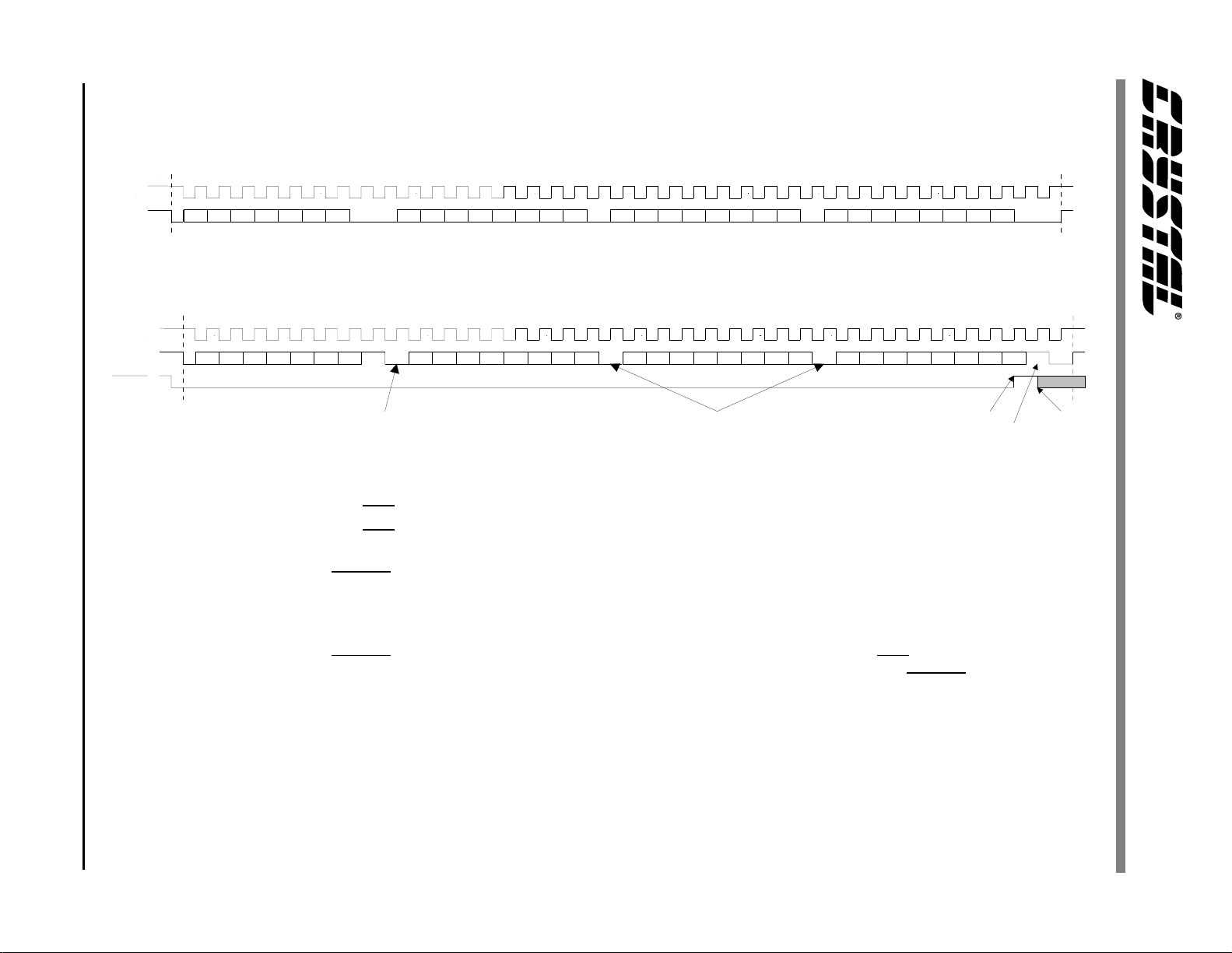
40 DS262F2
I2C Start I2C Stop
SCCLK
SCDIO
AD5
AD6 AD4
AD3 AD2 AD1 AD0 R/W D7 D6 D5 D4 D3
D2
D1 ACKD0ACK D7 D6 D5
D4
D3 D2 D1 ACKD0 D7
D6
D5 D4 D3 D2 D1 ACKD0
I2C Write Functional Timing
I2C Start I2C Stop
SCCLK
SCDIO
INTREQ
AD6
AD5 AD3 AD2 AD1 AD0 R/W D7 D6 D5 D4 D3 D2
AD4
ACKD0ACK D7 D6 D5 D4
D1
D2 D1 ACKD0 D7 D6
D3
D4 D3 D2 D1 NACKD0
D5
Note 1 Note 2 Note 3
Notes: 1. The ACK
2. The ACK
host.
3. INTREQ
be transferred out of the CS4923/4/5/6/7/8/9
4. A NOACK should be sent by the host after the last byte read to indicate the end of the read
cycle.
5. INTREQ
bit) at which point it may go low again if there is new data to be read. The condition of INTREQ
going low at this point should be treated as a new read condition and a new start condition
followed by an address byte should be sent.
I2C Read Functional Timing
for the address byte is driven by the CS4923/4/5/6/7/8/9.
s for the data bytes being read from the CS4923/4/5/6/7/8/9 should be driven by the
is guaranteed to stay low until the rising edge of SCCLK for last bit of the last byte to
is guaranteed to stay high until the next rising edge of SCCLK (for the ACK/NACK
Figure 20. I2C Timing
Note 4
Note 5
CS4923/4/5/6/7/8/9
CS4923/4/5/6/7/8/9
Following the address byte the host must clock out
an acknowledge from the part.
After the address byte, the host should clock out data
from the device one byte at a time until INTREQ is
no longer low. The host shifts data using the rising
edge of SCCLK. The data is valid on the rising edge
of SCCLK and transitions on the falling edge. After
each byte the host must send an acknowledge (ACK)
to the CS492X. While reading from the CS492X, an
acknowledge is defined as SCDIO being driven low
by the host for one SCCLK period after each byte. In
I2C mode, the INTREQ pin is deasserted
immediately following the rising edge of the last
data bit of the current byte being transferred if there
is no more data to be read. The INTREQ pin is
guaranteed to stay deasserted (high) until the rising
edge of SCCLK for the acknowledge bit.
For a more thorough look at I2C communication
and critical additional information on INTREQ
behavior reference the CS4923/4/5/6/7/8/9
Hardware User’s Guide.
6.5 External Memory
If using one of the serial modes, i.e. SPI o r I2C, the
system designer has the option of using external
memory. The external memory interface is not
compatible with the parallel modes since there are
shared pins that are needed by each mode. If using
the CS4926 or CS4928 for DTS decode, external
memory is required for external DTS tables.
The external memory interface is implemented on
the CS4923/4/5/6/7/8/9 with the following signals:
EMAD[7:0], EXTMEM and EMOE. Table 9 shows
the pin name, pin description and pin number of each
signal on the CS4923/4/5/6/7/8 /9. EMAD[7:0] serve
as a multiplexed address and data bus. EMOE is an
active-low external-memory data output enable as
well as the address latch strobe. EXTMEM serves as
the active low chip select output. Figure 21 illustrates
one possible external memory architecture for the
CS4923/4/5/6/7/8/9. Figure 22 shows the functional
timing of a run-time memory access .
Pin
Pin Name Pin Description
/EMOE * External Memory Output
Enable & Address Latch
Strobe
/EMWR * External Memory Write
Strobe
/EXTMEM External Memory Select 21
EMAD7 Address and Data Bit 7 8
EMAD6 Address and Data Bit 6 9
EMAD5 Address and Data Bit 5 10
EMAD4 Address and Data Bit 4 11
EMAD3 Address and Data Bit 3 14
EMAD2 Address and Data Bit 2 15
EMAD1 Address and Data Bit 1 16
EMAD0 Address and Data Bit 0 17
* - These pins must be configured appropriately to select a
serial host communication mode for the CS4923/4 /5/6/7/8/9
at the rising edge of RESET
Table 9. Memory Interface Pins
Number
5
4
The external memory interface was designed
primarily for two purposes: 1) Autoboot and/or 2)
real time external data access. The hardware
implementation for either mode can be the same but
the ROM access time requirements may differ. The
CS4923/4/5/6/7/8/9 Hardware User’s Guide should
be referenced for more information including
memory paging options to support both autoboot and
real time access as well as ROM speed requirements.
The external memory address is capable of addressing
between 64 kilobytes and 16 megabytes through a 16
to 24 bit addressing scheme. The address comes from
the DSP writing two or three initial bytes of address
consecutively on EMAD[7:0]. Each byte of address is
externally latched with the rising edge of EMOE while
EXTMEM is high. After the 2 or 3-byte address is
latched externally, the CS4923/4/5/6/7/8/9 then drives
EXTMEM and EMOE low simultaneously to select
the external memory. During this time the data is read
by the CS492X.
DS262F2 41

Only one of R3 and R4 shou
3.3V
CS4923/4/5/6/7/8/9
8
EMAD[7:0] DAT A[7:0]
CS4923/4/5/6/7/8/9
EMOE
EXTMEM
EMWR
ADDR[7:0]
AD DR[15:8]
DQ
8 BIT
'574
DFF
3.3V
3.3V 3.3V
DQ
8 BIT
'574
DFF
Only one of R1 and R2 should be stuffed.
The state of EMOE and EMWR at the
R1 R3
rising edge of RESET will determine the
serial mode that the part comes up in
while using external memory. Please see
R2 R4
section 2, Serial Communication for
more details.
Figure 21. External Memory Interface
ADDR[7:0]
AD DR[15:8]
OE
64K X 8
CS
ROM
ld be stuffed.
EXTMEM
EMOE
EMAD7:0 MA15:8 MA7:0 Data7:0
Figure 22. Run-Time Memory Access
42 DS262F2

CS4923/4/5/6/7/8/9
Although the memory can use more address bits,
typically only 16 bits of address space are used. For
this reason the memory example shown
incorporates a 2 latch memory architecture.
The two latch external memory architecture is
required for the CS4926 or CS4928 when using
DTS. A three latch architecture can not be used
with the CS4926 or CS4928 running DTS since the
run time memory access uses only 2 address cycles.
6.5.1 External Memory and Autoboot
To configure the CS4923/4/5/6/7/8/9 to
automatically load its code from external memory,
the ABOOT signal should be driven low at the
rising ed ge of RESET. Once agai n this mode can
only be chosen if either SPI or I2C serial
communication is being used. In serial control port
mode, holding the ABOOT pin low as the CS492X
leaves the reset state enables an automatic boot.
ABOOT can be released following the rising edge
of RESET. During the automatic boot cycle, the
serial control port should remain idle. Figure 23
shows an autoboot functional timing example.
The autoboot cycle actually is a 24 bit, or three
address byte cycle. It should be noted that for
autoboot, the most significant byte is always zero.
For this reason a two latch external memory
configuration can be used for autoboot. The higher
order address byte simply shifts out of the memory
latch and is discarded. If desired, a three latch
interface could also be used with the
CS4923/4/5/7/9 but it is not necessary.
For more information about autoboot and for a
thorough description of different external memory
architectures, reference the CS4923/4/5/6/7/8/9
Hardware User’s Guide.
RESET
ABOOT
EXTMEM
EMOE
EMWR
EMAD7:0 MA23:16 MA15:8 MA7:0 Data7:0
Figure 23. Autoboot Timing Diagram
DS262F2 43

CS4923/4/5/6/7/8/9
7. DIGITAL INPUT & OUTPUT
The CS4923/4/5/6/7/8/9 supports a wide variety of
data input and output mechanisms through various
input and output ports. Hardware availability is
entirely dependent on whether the software
application code being used supports the required
mode. This data sheet presents most of the modes
available with the CS4923/4/5/6/7/8/9 hardware.
This does not mean that all of the modes are
available with any particular piece of application
code. Both the CS4923/4/5/6/7/8/9 Hardware
User’s Guide and the application code user’s guide
for the particular code being used should be
referenced to determine if a particular mode is
supported.
7.1 Digital Audio Formats
This subsection will describe some common audio
formats that the CS4923/4/5/6/7/8/9 supports. It
should be noted that the input ports use up to 24-bit
PCM resolution and 16-bit compressed data word
lengths. The output port of the CS492X provides
up to 20-bit PCM resolution.
I2S: Figure 24 shows the I2S format. For I2S, data is
presented most significant bit first, one SCLK
delay after the transition of LRCLK and is valid on
the rising edge of SCLK. For the I2S format, t he left
subframe is presented when LRCLK is low and the
right subframe is presented when LRCLK is high.
SCLK is required to run at a frequency of 48Fs or
greater on the input ports.
Left Justified: Figure 25 shows the left justified
format with a rising edge SCCLK. Data is
presented most significant bit first on the first
SCLK after an LRCLK transition and is valid on
the rising edge of SCLK. For the left justified
format, the left subframe is presented when
LRCLK is high and the right subframe is presented
when LRCLK is low. The left justified format can
also be programmed for data to be valid on the
falling edge of SCLK. SCLK is required to run at a
frequency of 48Fs or greater on the input ports.
Right Justified: Figure 26 shows the right justified
format. The right justified format is similar to the
left justified format except the least significant bit
is right justified to be valid on the last transition of
SCLK before an LRCLK transition. Data is still
presented most significant bit first. For the right
justified format, the left subframe is presented
when LRCLK is high and the right subframe is
presented when LRCLK is low. The right justified
format can also be programmed for data being valid
on the falling edge of SCLK. SCLK is required to
run at a frequency of 48Fs or greater on the input
ports.
Multi-Channel: Figure 27 shows the multichannel format. In this format up to 6 channels of
audio are presented on one data line with 20 bits per
channel. Channels 0, 2, and 4 are presented while
the LR-CLK is high and channels 1, 3, 5 are
presented while the LRCLK is low. Data is valid on
the rising edge of SCLK and is presented most
significant bit first.
Because each of the ports is fully configurable,
there may be modes that can be supported which
are not presented.
44 DS262F2

CS4923/4/5/6/7/8/9
LRCK
Left Right
SCLK
SDATA MSB LSB
Figure 24. I
LRCK
SCLK
SDATA MSB LSB
Left Right
Figure 25. Left Justified Format
MSB LSB
2
S Format
MSB LSB MSB
LRCLK
SCLK
SDATA
SCLK
SDATA
MSB LSB
M Clocks
Per Channel
MSB LSB
M Clocks
Per Channel
Figure 27. M u lti-Chann el Format (M == 20)
Left RightLRCLK
MSB LSBLSB MSB LSB
Figure 26. Right Justified
MSB LSB
M Clocks
Per Channel
MSB LSB
M Clocks
Per Channel
MSB LSB
M Clocks
Per Channel
MSB LSB
M Clocks
Per Channel
MSB
DS262F2 45

CS4923/4/5/6/7/8/9
7.2 Digital Audio Input Port
The digital audio input port, or DAI, is used for
both compressed and PCM digital audio data input.
In addition this port supports a special clocking
mode in which a clock can be input to directly drive
the internal 33 bit counter. Table 10 shows the pin
names, mnemonics and pin numbers associated
with the DAI.
Pin Name Pin Description Pin Number
SDATAN1 Serial Data In 22
SCLKN1 Serial Bit Clock 25
LRCLKN1 Frame Clock 26
Table 10. Digital Audio Input Port
The DAI can be programmed to support I2S, left
justified and right justified data input. In addition
the DAI can be programmed for slave clocks,
where LRCLKN1 and SCLKN1 are inputs, or
master clocks, where LRCLKN1 and SCLKN1 are
outputs. In order for clocks to be master, the
internal PLL must be used.
STCCLK2 can also be programmed to drive the
internal 33 bit counter. This counter would
typically be driven by a 90kHz clock. The internal
counter is used by certain application code for
audio/video synchronization purposes.
7.3 Compressed Data Input Port
The compressed data input port, or CDI, can be
used for both compressed and PCM data input.
Table 11 shows the mnemonic, pin name and pin
number of the pins associated with the CDI port on
the CS4923/4/5/6/7/8/9.
Pin Name Pin Description Pin Number
SDATAN2
CMPDATA
SCLKN2
CMPCLK
LRCLKN2
CMPREQ
Table 11. Compressed Data Input Port
Serial Data In
Compressed Data In
Serial Bit Clock 28
Frame Clock
Data Request Out
27
29
The CDI can be configured to support I2S, left
justified and right justified formats. The CDI can
also be programmed for slave clocks, where
LRCLKN2 and SCLKN2 are inputs, or master
clocks, where LRCLKN2 and SCLKN2 are
outputs. In order for clocks to be mastered, the
internal PLL must be used.
In addition the CDI can be configured for bursty
compressed data input. Bursty audio delivery is a
special format in which only clock (CMPCLK) and
data (CMPDAT) are used to deliver compressed
data to the CS4923/4/5/6/7/8/9 (i.e. no frame clock
or LRCLK). A third line, CMPREQ, is used to
request more data from the host. It is an indicator
that the CS492X internal FIFO is low on data and
can accept another burst. Typically this mode is
used for compressed data delivery where
asynchronous data transfer occurs in the system,
i.e. in a system such as a set-top box or HDTV.
PCM data can not be presented in this mode since
data is interpreted as a continuous stream with no
word boundaries.
7.4 Parallel Digital Audio Data Input
If using the Intel or Motorola P arallel host interface
mode, the system designer can also choose to
deliver data through the byte wide parallel port.
The compressed data input register receives bytes
of data when the host interface writes to address
11b (A1 and A0 are both high). The host interface
port also utilizes the CMPREQ pin and the MFB
and MFC flags in the CONTROL register, which
are configurable to supply a data request flag at
different input buffer thresholds. CMPREQ acts as
an almost full flag. The CS4923/4/5/6/7/8/9 can
safely receive different size blocks of data
depending on the level of the input buffer
threshold. The threshold level is programmable and
the default level may differ between applications.
This mode reduces the polling burden associated
with hand-feeding the compressed data.
46 DS262F2

CS4923/4/5/6/7/8/9
In parallel host mode, the CS4923/4/5/6/7/8/9 can
accept PCM data written through the byte-wide
host interface to address 10b (A1 high, A0 low). In
this mode, there is a close connection between the
CS4923/4/5/6/7/8/9 application code and the host
processor that is delivering the PCM data. The
PCMRST bit of the CONTROL register provides
absolute software/hardware synchronization by
initializing the input channel to uniquely recognize
the first write to the byte-wide PCMDATA port.
Toggling PCMRST high and low informs the DSP
that the next sample read from the PCMDATA port
is the first sample of the left channel. In this
fashion, the CS492X can translate successive byte
writes into a variable number of channels with a
variable PCM sample size. In the mos t simple case,
the CS492X can receive stereo 8-bit PCM one byte
at a time with the internal DSP assigning the first
8-bit write (after PCMRST) to the left channel and
the second 8-bit write to the right channel. For
16-bit PCM, it assigns the first two 8-bit writes
(after PCMRST) to the left channel and the next
two writes to the right channel.
7.5 Digital Audio Output Port
The Digital Audio Output port, or DAO, is the port
used for digital output from the DSP. Table 12
shows the signals associated with the DAO. As
there are many modes that are firmware
configurable on the DAO, please consult the
Hardware User’s Guide and the application code
user’s guides to determine which modes are
supported by the download code being used.
Pin Name Pin Description Pin Number
AUDAT2 Serial Data In 39
AUDAT1 Serial Data In 40
AUDAT0 Serial Data In 41
LRCLK Frame Clock 42
SCLK Serial Bit Clock 43
MCLK Master Clock 44
XMT958 IEC60958 Transmitter 3
Table 12. Digital Audio Output Port
MCLK is the master clock and is firmware
configurable to be either an input or an output. If
MCLK is to be used as an output, the internal PLL
must be used. As an output MCLK can be
configured to provide a 128Fs, 256Fs or 512Fs
clock, where Fs is the output sample rate.
SCLK is the bit clock used to clock data out on
AUDATA0, AUDATA1 and AUDATA2. LRCLK
is the data framing clock whose frequency is
typically equal to the sampling frequency. Both
LRCLK and SCLK can be configured as either
inputs (Slave mode) or outputs (Master mode).
When LRCLK and SCLK are configured as inputs,
MCLK is a don’t care as an input. When LRCLK
and SCLK are configured as outputs, they are
derived from MCLK. Whether MCLK is
configured as an input or an output, an internal
divider from the MCLK signal is used to produce
LRCLK and SCLK. The ratios shown in table 13
give the possible SCLK values for different MCLK
frequencies (all values in terms of the sampling
frequency, Fs).
MCLK
(Fs)
128 X X
384** X X X
256 X X X X
512 X XXXX
** For MCLK as an input only
32 48 64 128 256 512
Table 13. MCLK/SCLK Master Mode Ratios
SCLK (Fs)
AUDAT0 is configurable to provide six, four, or
two channels. AUDAT1 and AUDAT2 can both
output two channels of data. Typically all three
AUDAT outputs are used in left justified, I2S or
right justified modes. In this way all six channels of
surround (Left, Center, Right, Left Surround, Right
Surround and Subwoofer) are provided.
Alternatively the multi-channel mode can be
configured to provide single data line multichannel support. Please consult the Hardware
User’s Guide and the application code user’s
DS262F2 47

CS4923/4/5/6/7/8/9
guides to determine which modes are supported by
the download code being used.
Serial digital audio data bit placement and sample
alignment is fully configurable in the
CS4923/4/5/6/7/8/9 including left justified, right
justified, delay bits or no delay bits, variable
sample word sizes, variable output channel count,
and programmable output channel pin assignments
and clock edge polarity to integrate with most
digital audio interfaces. If a mode is needed which
is not supported, please consult your Crystal
Representative as to its availability.
7.5.1 IEC60958 Output
The XMT958 output provides a CMOS level bi
phase encoded output. The XMT958 function can
be internally clocked from the PLL or from an
MCLK input if MCLK is 256Fs or 512Fs. All
channel status information can be used when using
software which supports this functionality. This
output can be used for either 2 channel PCM output
or compressed data output in accordance with
IEC61937. To be fully IEC60958 compliant this
output would need to be buffered through an
RS422 device or an optocoupler as its outputs are
only CMOS. Please consult the
CS4923/4/5/6/7/8/9 Hardware User’s Guide and an
application code user’s guide to determine if this
pin is supported by the download code being used.
48 DS262F2

8. PIN DESCRIPTIONS
VD1
DGND1
XMT958
WR,DS,EMWR,GPIO10
RD,R/W,EMOE,GPIO11
A1, SCDIN
A0, SCCLK
DATA7,EMAD7,GPIO7
DATA6,EMAD6,GPIO6
DATA5,EMAD5,GPIO5
DATA4,EMAD4,GPIO4
VD2
DGND2
DATA3,EMAD3,GPIO3
DATA2,EMAD2,GPIO2
DATA1,EMAD1,GPIO1
DATA0,EMAD0,GPIO0
SCDIO, SCDOUT,PSEL,GPIO9
ABOOT, INTREQ
EXTMEM, GPIO8
SDATAN1
CS
6 5 4 3 2 1 44 43 42 41 40
7
8
9
10
11
12
13
14
15
16
17
1819 20 21 22 23 24 252627 28
CS4923-CL
44-pin PLCC
Top View
39
38
37
36
35
34
33
32
31
30
29
CS4923/4/5/6/7/8/9
MCLK
SCLK
LRCLK
AUDATA0
AUDATA1
AUDATA2
DC
DD
RESET
AGND
VA
FILT1
FILT2
CLKSEL
CLKIN
CMPREQ, LRCLKN2
CMPCLK, SCLKN2
CMPDAT, SDATAN2
LRCLKN1
SCLKN1, STCCLK2
DGND3
VD3
VA—Analog Positive Supply: Pin 34
Analog positive supply for clock generator. Nominally +3.3 V.
AGND—Analog Supply Ground: Pin 35
Analog ground for clock generator PLL.
VD1, VD2, VD3—Digital Positive Supply: Pins 1, 12, 23
Digital positive supplies. Nominally +3.3 V.
DGND1, DGND2, DGND3—Digital Supply Ground: Pins 2, 13, 24
Digital ground.
FILT1—Phase-Locked Loop Filter: Pin 33
Connects to an external filter for the on-chip phase-locked loop. This pin does not meet Cirrus
Logic’s ESD tolerance of 2000 V using the human body model. This pin will tolerate ESD of
1000 V using the human body model.
DS262F2 49

FILT2—Phase Locked Loop Filter: Pin 32
Connects to an external filter for the on-chip phase-locked loop. This pin does not meet Cirrus
Logic’s ESD tolerance of 2000 V using the human body model. This pin will tolerate ESD of
1000 V using the human body model.
CLKIN—Master Clock Input: Pin 30
CS4923/4/5/6/7/8/9 clock input. When in internal clock mode (CLKSEL == DGND), this input
is connected to the internal PLL from which all internal clocks are derived. When in external
clock mode (CLKSEL == VD), this input is connected to the DSP clock. INPUT
CLKSEL—DSP Clock Select: Pin 31
This pin selects the clock mode of the CS4923/4/5/6/7/8/9. When CLKSEL is low, CLKIN is
connected to the internal PLL from which all internal clocks are derived. When CLKSEL is
high CLKIN is connected to the DSP clock. INPUT
DATA7, EMAD7, GPIO7—Pin 8
DATA6, EMAD6, GPIO6—Pin 9
DATA5, EMAD5, GPIO5—Pin 10
DATA4, EMAD4, GPIO4—Pin 11
DATA3, EMAD3, GPIO3—Pin 14
DATA2, EMAD2, GPIO2—Pin 15
DATA1, EMAD1, GPIO1—Pin 16
DATA0, EMAD0, GPIO0—Pin 17
CS4923/4/5/6/7/8/9
In parallel host mode, these pins provide a bidirectional data bus. If a serial host mode is
selected, these pins can provide a multiplexed address and data bus for connecting an 8-bit
external memory. Otherwise, in serial host mode, these pins can act as general-purpose input or
output pins that can be individually configured and controlled by the DSP.
BIDIRECTIONAL - Default: INPUT
A0, SCCLK—Host Parallel Address Bit Zero or Serial Control Port Clock: Pin 7
In parallel host mode, this pin serves as one of two address input pins used to select one of four
parallel registers. In serial host mode, this pin serves as the serial control clock signal,
specifically as the SPI clock input or the I2C clock input. INPUT
A1, SCDIN—Host Parallel Address Bit One or SPI Serial Control Data Input: Pin 6
In parallel host mode, this pin serves as one of two address input pins used to select one of four
parallel registers. In SPI serial host mode, this pin serves as the data input. INPUT
RD, R/W, EMOE, GPIO11—Host Parallel Output Enable or Host Parallel R/W or External
Memory Output Enable or General Purpose Input & Output Number 11: Pin 5
In Intel parallel host mode, this pin serves as the active-low data bus enable input. In Motorola
parallel host mode, this pin serves as the read-high/write-low control input signal. In serial host
mode, this pin can serve as the external memory active-low data-enable output signal. Also in
serial host mode, this pin can serve as a general purpose input or output bit.
BIDIRECTIONAL - Default: INPUT
50 DS262F2
CS4923/4/5/6/7/8/9
WR, DS, EMWR, GPIO10—Host Write Strobe or Host Data Strobe or External Memory Write
Enable or General Purpose Input & Output Number 10: Pin 4
In Intel parallel host mode, this pin serves as the active-low data-write-input strobe. In
Motorola parallel host mode, this pin serves as the active-low data-strobe-input signal. In serial
host mode, this pin can serve as the external-memory active-low write-enable output signal.
Also in serial host mode, this pin can serve as a general purpose input or output bit.
BIDIRECTIONAL - Default: INPUT
CS—Host Parallel Chip Select, Host Serial SPI Chip Select: Pin 18
In parallel host mode, this pin serves as the active-low chip-select input signal. In serial host
SPI mode, this pin is used as the active-low chip-select input signal. INPUT
RESET—Master Reset Input: Pin 36
Asynchronous active-low master reset input. Reset should be low at power-up to initialize the
CS4923/4/5/6/7/8/9 and to guarantee that the device is not active during initial power-on
stabilization periods. At the rising edge of reset the host interface mode is selected contingent
on the state of the RD, WR and PSEL pins. Additionally, an autoboot sequence can be initiated
if a serial control mode is selected and ABOOT is held low. If reset is low all bidirectional pins
are high impedance inputs. INPUT
SCDIO, SCDOUT, PSEL, GPIO9—Serial Control Port Data Input and Output, Parallel Port
Type Select: Pin 19
In I2C mode, this pin serves as the open-drain bidirectional data pin. In SPI mode this pin
serves as the data output pin. In parallel host mode, this pin is sampled at the rising edge of
RESET to configure the parallel host mode as an Intel type bus or as a Motorola type bus. In
parallel host mode, after the bus mode has been selected, the pin can function as a generalpurpose input or output pin. BIDIRECTIONAL - Default: INPUT
In I2C mode this pin is an OPEN DRAIN I/O and requires a 4.7k Pull-Up
EXTMEM, GPIO8—External Memory Chip Select or General Purpose Input & Output Number
8: Pin 21
In serial control port mode, this pin can serve as an output to provide the chip-select for an
external byte-wide ROM. In parallel and serial host mode, this pin can also function as a
general-purpose input or output pin. BIDIRECTIONAL - Default: INPUT
INTREQ, ABOOT—Control Port Interrupt Request, Automatic Boot Enable: Pin 20
Open-drain interrupt-request output. This pin is driven low to indicate that the DSP has
outgoing control data and should be serviced by the host. Also in serial host mode, this signal
initiates an automatic boot cycle from external memory if it is held low through the rising edge
of reset. OPEN DRAIN I/O - Requires 4.7k Ohm Pull-Up
AUDATA2—Digital Audio Output 2: Pin 39
PCM multi-format digital-audio data output, capable of two-channel 20-bit output. This PCM
output defaults to DGND as output until enabled by the DSP software. OUTPUT
DS262F2 51

AUDATA1—Digital Audio Output 1: Pin 40
PCM multi-format digital-audio data output, capable of two-channel 20-bit output. This PCM
output defaults to DGND as output until enabled by the DSP software. OUTPUT
AUDATA0—Digital Audio Output 0: Pin 41
PCM multi-format digital-audio data output, capable of two-, four-, or six-channel 20-bit
output. This PCM output defaults to DGND as output until enabled by the DSP software.
OUTPUT
MCLK—Audio Master Clock: Pin 44
Bidirectional master audio clock. MCLK can be an output from the CS4923/4/5/6/7/8/9 that
provides an oversampled audio-output clock at either 128 Fs, 256 Fs, or 512 Fs. MCLK can be
an input at 128 Fs, 256 Fs, 384 Fs, or 512 Fs. MCLK is used to derive SCLK and LRCLK
when SCLK and LRCLK are driven by the CS492X. BIDIRECTIONAL - Default: INPUT
SCLK—Audio Output Bit Clock: Pin 43
Bidirectional digital-audio output bit clock. SCLK can be an output that is derived from MCLK
to provide 32 Fs, 64 Fs, 128 Fs, 256 Fs, or 512 Fs, depending on the MCLK rate and the
digital-output configuration. SCLK can also be an input and must be at least 48Fs or greater.
As an input, SCLK is independent of MCLK. BIDIRECTIONAL - Default: INPUT
CS4923/4/5/6/7/8/9
LRCLK—Audio Output Sample Rate Clock: Pin 42
Bidirectional digital-audio output-sample-rate clock. LRCLK can be an output that is divided
from MCLK to provide the output sample rate depending on the output configuration. LRCLK
can also be an input. As an input LRCLK is independent of MCLK.
BIDIRECTIONAL - Default: INPUT
XMT958—SPDIF Transmitter Output: Pin 3
CMOS level output that contains a biphase-encoded clock for synchronously providing two
channels of PCM digital audio or a IEC61937 compressed-data interface or both. This output
typically connects to the input of an RS-422 transmitter or to the input of an optical transmitter.
OUTPUT
SCLKN1, STCCLK2—PCM Audio Input Bit Clock: Pin 25
Bidirectional digital-audio bit clock that is an output in master mode and an input in slave
mode. In slave mode, SCLKN1 operates asynchronously from all other CS492X clocks. In
master mode, SCLKN1 is derived from the CS492X internal clock generator. In either master
or slave mode, the active edge of SCLKN1 can be programmed by the DSP. For applications
supporting PES layer synchronization this pin can be used as STCCLK2, which provides a path
to the internal STC 33 bit counter. BIDIRECTIONAL - Default: INPUT
52 DS262F2

LRCLKN1—PCM Audio Input Sample Rate Clock: Pin 26
Bidirectional digital-audio frame clock that is an output in master mode and an input in slave
mode. LRCLKN1 typically is run at the sampling frequency. In slave mode, LRCLKN1
operates asynchronously from all other CS492X clocks. In master mode, LRCLKN1 is derived
from the CS492X internal clock generator. In either master or slave mode, the polarity of
LRCLKN1 for a particular subframe can be programmed by the DSP.
BIDIRECTIONAL - Default: INPUT
SDATAN1—PCM Audio Data Input Number One: Pin 22
Digital-audio data input that can accept from one to six channels of compressed or PCM data.
SDATAN1 ca n be sampled with either edge of SCLKN1, depending on how SCLKN1 has been
configured. INPUT
CMPCLK, SCLKN2—PCM Audio Input Bit Clock: Pin 28
Bidirectional digital-audio bit clock that is an output in master mode and an input in slave
mode. In slave mode, SCLKN2 operates asynchronously from all other CS492X clocks. In
master mode, SCLKN2 is derived from the CS492X internal clock generator. In either master
or slave mode, the active edge of SCLKN2 can be programmed by the DSP. If the CDI is
configured for bursty delivery, CMPCLK is an input used to sample CMPDAT.
BIDIRECTIONAL - Default: INPUT
CS4923/4/5/6/7/8/9
CMPREQ, LRCLKN2—PCM Audio Input Sample Rate Clock: Pin 29
When the CDI is configured as a digital audio input, this pin serves as a bidirectional digitalaudio frame clock that is an output in master mode and an input in slave mode. LRCLKN2
typically is run at the sampling frequency. In slave mode, LRCLKN2 operates asynchronously
from all other CS492X clocks. In master mode, LRCLKN2 is derived from the CS492X
internal clock generator. In either master or slave mode, the polarity of LRCLKN2 for a
particular subframe can be programmed by the DSP. When the CDI is configured for bursty
delivery, or parallel audio data delivery is being used, CMPREQ is an output which serves as
an internal FIFO monitor. CMPREQ is an active low signal that indicates when another block
of data can be accepted. BIDIRECTIONAL - Default: INPUT
CMPDAT, SDATAN2—PCM Audio Data Input Number Two: Pin 27
Digital-audio data input that can accept from one to six channels of compressed or PCM data.
SDATAN2 ca n be sampled with either edge of SCLKN2, depending on how SCLKN2 has been
configured. Similarly CMPDAT is the compressed data input pin when the CDI is configured
for bursty delivery. When in this mode, the CS4923/4/5/6/7/8/9 internal PLL is driven by the
clock recovered from the incoming data stream. INPUT
DC—Reserved: Pin 38
This pin is reserved and should be pulled up with an external 4.7k resistor.
DD—Reserved: Pin 37
This pin is reserved and should be pulled up with an external 4.7k resistor.
DS262F2 53

9. PACKAGE DIMENSIONS
44L PLCC PACKAGE DRAWING
CS4923/4/5/6/7/8/9
e
D2/E2
B
D1
D
E1 E
A1
A
INCHES MILLIMETERS
DIM MIN MAX MIN MAX
A 0.165 0.180 4.043 4.572
A1 0.090 0.120 2.205 3.048
B 0.013 0.021 0.319 0.533
D 0.685 0.695 16.783 17.653
D1 0.650 0.656 15.925 16.662
D2 0.590 0.630 14.455 16.002
E 0.685 0.695 16.783 17.653
E1 0.650 0.656 15.925 16.662
E2 0.590 0.630 14.455 16.002
e 0.040 0.060 0.980 1.524
54 DS262F2

• Notes •

 Loading...